EP2928700B1 - Method and apparatus for transfer of films among substrates - Google Patents
Method and apparatus for transfer of films among substrates Download PDFInfo
- Publication number
- EP2928700B1 EP2928700B1 EP13860728.8A EP13860728A EP2928700B1 EP 2928700 B1 EP2928700 B1 EP 2928700B1 EP 13860728 A EP13860728 A EP 13860728A EP 2928700 B1 EP2928700 B1 EP 2928700B1
- Authority
- EP
- European Patent Office
- Prior art keywords
- substrate
- layer
- solution
- cathode
- anode
- Prior art date
- Legal status (The legal status is an assumption and is not a legal conclusion. Google has not performed a legal analysis and makes no representation as to the accuracy of the status listed.)
- Active
Links
Images

Classifications
-
- B—PERFORMING OPERATIONS; TRANSPORTING
- B32—LAYERED PRODUCTS
- B32B—LAYERED PRODUCTS, i.e. PRODUCTS BUILT-UP OF STRATA OF FLAT OR NON-FLAT, e.g. CELLULAR OR HONEYCOMB, FORM
- B32B37/00—Methods or apparatus for laminating, e.g. by curing or by ultrasonic bonding
- B32B37/14—Methods or apparatus for laminating, e.g. by curing or by ultrasonic bonding characterised by the properties of the layers
- B32B37/24—Methods or apparatus for laminating, e.g. by curing or by ultrasonic bonding characterised by the properties of the layers with at least one layer not being coherent before laminating, e.g. made up from granular material sprinkled onto a substrate
-
- H—ELECTRICITY
- H01—ELECTRIC ELEMENTS
- H01L—SEMICONDUCTOR DEVICES NOT COVERED BY CLASS H10
- H01L21/00—Processes or apparatus adapted for the manufacture or treatment of semiconductor or solid state devices or of parts thereof
- H01L21/67—Apparatus specially adapted for handling semiconductor or electric solid state devices during manufacture or treatment thereof; Apparatus specially adapted for handling wafers during manufacture or treatment of semiconductor or electric solid state devices or components ; Apparatus not specifically provided for elsewhere
- H01L21/67005—Apparatus not specifically provided for elsewhere
- H01L21/67011—Apparatus for manufacture or treatment
- H01L21/67132—Apparatus for placing on an insulating substrate, e.g. tape
-
- B—PERFORMING OPERATIONS; TRANSPORTING
- B32—LAYERED PRODUCTS
- B32B—LAYERED PRODUCTS, i.e. PRODUCTS BUILT-UP OF STRATA OF FLAT OR NON-FLAT, e.g. CELLULAR OR HONEYCOMB, FORM
- B32B38/00—Ancillary operations in connection with laminating processes
- B32B38/08—Impregnating
-
- B—PERFORMING OPERATIONS; TRANSPORTING
- B32—LAYERED PRODUCTS
- B32B—LAYERED PRODUCTS, i.e. PRODUCTS BUILT-UP OF STRATA OF FLAT OR NON-FLAT, e.g. CELLULAR OR HONEYCOMB, FORM
- B32B38/00—Ancillary operations in connection with laminating processes
- B32B38/10—Removing layers, or parts of layers, mechanically or chemically
-
- C—CHEMISTRY; METALLURGY
- C01—INORGANIC CHEMISTRY
- C01B—NON-METALLIC ELEMENTS; COMPOUNDS THEREOF; METALLOIDS OR COMPOUNDS THEREOF NOT COVERED BY SUBCLASS C01C
- C01B32/00—Carbon; Compounds thereof
- C01B32/15—Nano-sized carbon materials
- C01B32/182—Graphene
- C01B32/184—Preparation
-
- C—CHEMISTRY; METALLURGY
- C01—INORGANIC CHEMISTRY
- C01B—NON-METALLIC ELEMENTS; COMPOUNDS THEREOF; METALLOIDS OR COMPOUNDS THEREOF NOT COVERED BY SUBCLASS C01C
- C01B32/00—Carbon; Compounds thereof
- C01B32/15—Nano-sized carbon materials
- C01B32/182—Graphene
- C01B32/194—After-treatment
-
- H—ELECTRICITY
- H01—ELECTRIC ELEMENTS
- H01L—SEMICONDUCTOR DEVICES NOT COVERED BY CLASS H10
- H01L21/00—Processes or apparatus adapted for the manufacture or treatment of semiconductor or solid state devices or of parts thereof
- H01L21/02—Manufacture or treatment of semiconductor devices or of parts thereof
- H01L21/02002—Preparing wafers
- H01L21/02005—Preparing bulk and homogeneous wafers
- H01L21/02008—Multistep processes
- H01L21/0201—Specific process step
-
- H—ELECTRICITY
- H01—ELECTRIC ELEMENTS
- H01L—SEMICONDUCTOR DEVICES NOT COVERED BY CLASS H10
- H01L21/00—Processes or apparatus adapted for the manufacture or treatment of semiconductor or solid state devices or of parts thereof
- H01L21/67—Apparatus specially adapted for handling semiconductor or electric solid state devices during manufacture or treatment thereof; Apparatus specially adapted for handling wafers during manufacture or treatment of semiconductor or electric solid state devices or components ; Apparatus not specifically provided for elsewhere
- H01L21/67005—Apparatus not specifically provided for elsewhere
- H01L21/67011—Apparatus for manufacture or treatment
- H01L21/67092—Apparatus for mechanical treatment
-
- B—PERFORMING OPERATIONS; TRANSPORTING
- B32—LAYERED PRODUCTS
- B32B—LAYERED PRODUCTS, i.e. PRODUCTS BUILT-UP OF STRATA OF FLAT OR NON-FLAT, e.g. CELLULAR OR HONEYCOMB, FORM
- B32B37/00—Methods or apparatus for laminating, e.g. by curing or by ultrasonic bonding
- B32B37/14—Methods or apparatus for laminating, e.g. by curing or by ultrasonic bonding characterised by the properties of the layers
- B32B37/24—Methods or apparatus for laminating, e.g. by curing or by ultrasonic bonding characterised by the properties of the layers with at least one layer not being coherent before laminating, e.g. made up from granular material sprinkled onto a substrate
- B32B2037/243—Coating
-
- B—PERFORMING OPERATIONS; TRANSPORTING
- B32—LAYERED PRODUCTS
- B32B—LAYERED PRODUCTS, i.e. PRODUCTS BUILT-UP OF STRATA OF FLAT OR NON-FLAT, e.g. CELLULAR OR HONEYCOMB, FORM
- B32B37/00—Methods or apparatus for laminating, e.g. by curing or by ultrasonic bonding
- B32B37/14—Methods or apparatus for laminating, e.g. by curing or by ultrasonic bonding characterised by the properties of the layers
- B32B37/24—Methods or apparatus for laminating, e.g. by curing or by ultrasonic bonding characterised by the properties of the layers with at least one layer not being coherent before laminating, e.g. made up from granular material sprinkled onto a substrate
- B32B2037/246—Vapour deposition
Definitions
- the present application generally relates to methods and apparatus for transfer of films from one or more substrates to another.
- graphene is a single atomic layer of carbon atoms, tightly bonded in a hexagonal lattice.
- graphene has already revealed exciting new physics including "relativistic" carriers with implications for quantum electronic transport and charge screening, a width-dependent energy band gap, extremely high carrier mobility, high elasticity and electromechanical modulation.
- the properties of graphene appeal to many industries, in particular electronics.
- Graphene's high carrier mobility and high thermal conductivity make it a potential alternative to silicon and diamond. Its properties may enable the creation of next generation solid-state devices (ballistic transistors, spin transistors, etc.).
- Graphene is also a candidate for use as a flexible, optically transparent conductor in applications such as touch displays and photovoltaics.
- Other potential applications include chemical sensors, nanopore filters, impermeable coatings for corrosion and/or chemical protection, ultracapacitors, TEM supports, and others.
- One current, widely used graphene transfer process includes a chemical etching step to remove the metal substrate by dissolution. Scaling this process to thousands of square meters production, leads to great expense and waste challenges. The reclamation or disposal of metal infused etchant constitutes a major cost and waste handling issue. Since the substrate is dissolved by the etchant, it cannot be reused for the growth of graphene films. In addition, the dissolution process is rather slow. For at least these reasons, this conventional technique is not well-suited for efficient, large-scale, low cost production of graphene films.
- WO2012/067438 A2 discloses a method for transferring a graphene layer from a catalyst metal onto a substrate film.
- Article " Electrochemical Delamination of CVD-Grown Graphene Film: Toward the Recyclable Use of Copper Catalyst"; American Chemical Society; vol 5; No. 12; page 9927; (2011 ) discloses a separation method for separating chemical vapor deposited graphene from a metallic catalyst by transfer to a dielectric substrate.
- the present invention may address one or more of the problems and deficiencies of the prior art discussed above. However, it is contemplated that the invention may prove useful in addressing other problems and deficiencies, or provides benefits and advantages, in a number of technical areas. Therefore the claimed invention should not necessarily be construed as being limited to addressing any of the particular problems or deficiencies discussed herein.
- the present invention provides a method according to claim 1. by:
- first substrate in a first direction and the first pickup roll is constructed and arranged to pull the second substrate along with the at least one layer of material in a second direction, the first and second directions diverging from one another, thereby defining an angle of separation.
- a method of transferring graphene from a substrate on which it is formed to a second substrate attach the second substrate to the graphene, as described later, immerse the layers in a solution, and then use a mechanical pulling action to separate the graphene and second substrate from the original substrate with the aid of bubbles, formed electrolytically at the interface between the graphene and the metal, to push the two layers apart.
- An electrolysis cell is configured in the solution by electrically contacting the graphene and metal structure and a second electrode. This process is suitable for graphene films grown on conductive substrate. This process is especially suitable for scaling to larger area graphene films.
- At least one layer of material 12 can be formed on at least part of a surface of a first substrate 10 thereby forming an interface 16 between a first surface 14 of the at least one layer of material 12 and the substrate 10.
- the at least one layer material can be formed on part of a surface of the first substrate, for example, as a periodic pattern.
- the at least one layer of material 12 can cover the entire surface of the first substrate 10.
- the layer of material 12 can be formed as a single layer of material, or as multiple layers of material.
- the layer of material 12 can have any suitable thickness. The methods and arrangements of the present invention are advantageous with respect to thin layers, such as layers having a total thickness less than 10 nm.
- the at least one layer of material 12 can be formed from any suitable material, or combination of materials.
- the at least one layer of material 12 comprises graphene.
- the graphene may be present as a single atomic layer of graphene, or as layers of graphene having a multiple-atom thickness.
- the graphene can be combined with one or more additional materials.
- the graphene can be doped with one or more dopants.
- the dopant(s) can comprise iodine, nitrogen, boron, potassium, arsenic, gallium, aluminum, indium, or others.
- Graphene can be formed according to any suitable technique, generally known to those skilled in the art, such as exfoliation of graphite, epitaxial growth, oxide reduction of graphite, etching or division of carbon nanotubes, sonication of graphite, and carbon dioxide reduction reactions.
- graphene is grown on a substrate by chemical vapor deposition.
- the graphene may be grown onto a planarized substrate under relatively low temperature, near atmospheric pressure, conditions.
- the substrate 10 can be planarized by any suitable technique, such as electropolishing, mechanically polishing, and/or chemically polishing the surface thereof upon which graphene is to be grown.
- This surface of the substrate 10 is then contacted with a hydrocarbon gas (e.g., methane) at a temperature of about 250°C to about 2000°C, and at a pressure of about 10 -7 atmospheres to about ambient pressure.
- a hydrocarbon gas e.g., methane
- One suitable technique of forming graphene as the at least one layer material 12 upon the substrate 10 according to certain illustrative and non-limiting embodiments of the present invention is described in WO 2012/021677 , the entire contents of which is incorporated herein by reference.
- the first substrate 10 can be formed from any suitable material.
- the first substrate 10 can be flexible or rigid.
- the substrate 10 can be formed of a metal.
- metals that could be used to form the substrate 10 include copper, rhodium, ruthenium, iridium, platinum, cobalt, nickel, or any combination thereof.
- the substrate 10 is formed from copper.
- the first substrate 10 may have an optional layer or coating 11 applied to a surface thereof before or after the formation of material 12.
- the layer or coating 11 can be formed any suitable material or materials.
- it can be formed of a polymer, such as polyethylene terephthalate (PET), Poly(methyl methacrylate) (PMMA), Polyethylene naphthalate (PEN), polyamide, polytetrafluoroethylene (PTFE), polyethylene, and others.
- PET polyethylene terephthalate
- PMMA Poly(methyl methacrylate)
- PEN Polyethylene naphthalate
- PTFE polytetrafluoroethylene
- the layer or coating may be applied by any suitable technique, such as adhesive attachment, laminating, coating, spraying, spin coating, dipping, and the like.
- a second substrate 18 can be attached to a second surface of the at least one layer of material.
- the second substrate 18 can be formed from any suitable material, or combination of materials.
- the second substrate 18 can be formed from poly(methyl methacrylate) (PMMA) or polyethylene terephthalate (PET).
- the second substrate 18 could be formed from polyethylene (PE), polyvinylchloride (PVC), glass, silica, silicon dioxide, silicon, MgO, and others.
- the second substrate can be applied to the at least one layer of material by any suitable technique. Suitable techniques include, but not limited to adhesive attachment, laminating, coating, spraying, spin coating, dipping, and the like.
- the bubbles 12 can be formed by any suitable mechanism.
- the bubbles 22 are formed by the emission of hydrogen due to the electrolysis of water. This mechanism should be familiar to those skilled in the art.
- the other component utilized according to the principles of the present invention to delaminated or separate the aforementioned materials involve the application of mechanical force or pressure. This is schematically illustrated by the block arrows appearing in Figure 1 (C) . As illustrated therein, these forces are applied in directions which diverge from one another thereby defining a separation angle ⁇ .
- the effectiveness and efficiency of the delamination operation can be influenced through careful selection of the appropriate separation angle ⁇ , as well as the quantity of force applied.
- the separation angle ⁇ is about 1 degree to about 90 degrees, or about 5 degrees to about 60 degrees.
- the at least one layer of material 12 can be further transferred to an additional third substrate.
- FIG 2 An example of this alternative procedure is schematically illustrated in Figure 2 .
- the second substrate acts as a transfer film 18'.
- This transfer film 18' can be formed from any suitable material or combination of materials. It can be formed from the same material as the second substrate 18, as previously described above.
- the transfer film 18' can be formed from a different material such as heat transfer tape, PET, PE, PVC, PTFE, PMMA, and others.
- the transfer film 18' can be formed from a thermally-sensitive adhesive which breaks down upon exposure to elevated temperatures.
- a third substrate 24 is attached to a surface of the at least one layer material 12. See, e.g., Figure 2 (D) .
- the transfer film 18' is removed from the at least one layer of material 12, leaving the at least one layer material 12 disposed upon the end-use substrate 24. This removal can be accomplished by any suitable technique, such as the above-mentioned heating of a thermally-sensitive adhesive, mechanical force, chemical separation techniques, chemical dissolution, chemical etching, photoinduced degradation, and depolymerization.
- the at least one layer of material 12 can be transferred to a rigid substrate 24.
- the substrate 24 may also be flexible.
- the substrate 24 can be formed of any suitable material, such as a ceramic, metal or polymer. Specific illustrative, and non-limiting examples, include: silicon, glass, quartz, semiconductor films on rigid substrates.
- the present invention also encompasses arrangements, which can be, for example, utilized to carry out the aforementioned methods. Arrangements constructed according to the principles of the present invention are illustrated in Figures 3-5 . Those features illustrated therein which are also described above in connection with the aforementioned methods are identified using the same reference numerals utilized in Figures 1-2 . As illustrated, for example, in Figure 3 , the aforementioned method can be implemented as a roll-to-roll process. The arrangement depicted in Figure 3 is suitable for such roll-to-roll processes, but is not limited in this manner. As illustrated therein, the arrangement can comprise a number of different combinations of the illustrated features. For example, a supply roll 26 comprising a roll of composite material 28 can be provided.
- the composite material can comprise a first substrate 10, at least one layer material 12 in contact with the first substrate thereby defining interface 16, a second substrate 18 attached to a second surface of the at least one layer of material 12, and an optional additional layer or coating 11 disposed on a surface of the first substrate 10.
- These materials can take the specific forms or compositions previously mentioned above.
- the electrolytic cell comprises a vessel 30 containing a solution 32 the solution 32 comprises water and at least one electrolyte. Any suitable electrolyte, or combination of electrolytes, can be utilized. According to certain optional embodiments, the electrolyte comprises, for example, sodium hydroxide, potassium hydroxide, sulfuric acid, and/or sodium chloride.
- the solution comprises a 0.05 mole to 1 mole electrolyte per liter of water. Alternatively, the solution contains one or more dopant materials.
- Suitable dopants include, but are not limited to, iodine, nitrogen, boron, potassium, arsenic, gallium, aluminum, indium, chromium, or a number of organic molecules such as 2,3,5,6-Tetrafluoro-7,7,8,8-tetracyanoquinodimethane, 7,7,8,8-Tetracyano-2,3,5,6-tetrafluoroquinodimethane (F4-TCNQ).
- the solution may contain any suitable amount of dopant, which is highly dependent upon the dopant used.
- important properties of the film may be refined and improved by doping the graphene. For example, with the proper doping, the electronic carrier density in the graphene will be increased, increasing conductivity for a transparent contact. As a two dimensional material, in which all the material is an exposed surface, graphene may be doped after deposition because there is no need for the dopant to diffuse to deeper layers (as there are none).
- Doping of the graphene can be achieved during the transfer process by incorporating the dopant into the electrolyte solution. As the graphene is separated from the metal deposition substrate, it is exposed to the solution.
- the electrolyte in the solution or another additive serves as the dopant, adhering to the surface of the graphene during the process.
- the separation process does not require a particular electrolyte to function.
- the electrolyte increases the conductivity of the solution to enable charge transfer through the solution.
- electrolyte additives which will increase the solution conductivity. Accordingly, solution additives may be selected and mixed to achieve a targeted doping density and an effective graphene-metal separation. The process can be controlled and refined through control of the electrolyte makeup and the exposure duration through the geometry of the separation bath.
- the electrical bias on the graphene which is part of one of the electrodes in the electrolysis cell, can be used to draw dopants to the graphene surface, where it bonds or is adsorbed.
- the process may use more than one electrolyte. Multiple electrolytes can be used to control doping while maintaining the solution conductance for the separation process.
- the cell is completed by forming a cathode 34 at the composite material, and anode 36 located at a distance from the cathode, or "remotely" relative thereto.
- the anode can be located near the point of separation 16. Through placement of the anode, the formation of hydrogen bubbles can be focused toward the separation interface 16.
- the presence of the optional coating 11 on the first substrate 10 can serve to prevent electrolytic reaction on those surfaces of the first substrate 10 which is covered by the coating or layer 11, thereby effectively focusing the reaction at the interface 16 during the delamination or separation procedure.
- the cathode is negatively biased, and the anode is positively biased, and both are connected to a power source 38 which provides electrical current flows through the solution 32.
- a power source 38 which provides electrical current flows through the solution 32.
- Any suitable power source can be utilized and any appropriate voltage and current conditions can be applied.
- the power source can be constructed and arranged to generate electrical current having a current density of 0.5 A/cm 2 and voltage of 10V. The voltage is highly dependent upon the positioning of the electrodes.
- the essential location for gas formation to occur is at the point of separation 16. Gas bubbling will occur at every exposed conductive surface of the composite material cathode that is immersed in the solution. Power source construction should account for all current flow at the point of separation and elsewhere.
- hydrogen is emanated in gaseous form at the cathode 34 (which is the composite material 28), specifically bubbles 22 are formed at least at the interface 16 between the first substrate 10 and the at least one layer of material 12.
- the gas formation aiding the separation can be of a different composition by use of different chemistry and placement of anode and cathode.
- Other gas bubbling which may be employed by electrolysis or other electrochemical reactions include, for example, oxygen, nitrogen, or chlorine.
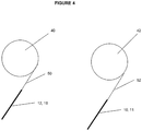
- the arrangement may further comprise a first pickup roll 40 the first pickup roll is attached to the second substrate 18 and the at least one layer material 12 disposed on a surface thereon. Connection of these materials to the pickup roll 40 can be facilitated by the use of a leader film 50, as illustrated in Figure 4 .
- the leader film 50 can be formed from any suitable material, such as a polymer. Suitable polymers include PET, PMMA, polyamide, PTFE, and polyethylene.
- optional guide roll 48 can be utilized to affect the direction by which the first substrate 10 and optional additional layer or coating 11 is pulled by the pickup roll 42. Therefore, as clearly illustrated in Figure 3 , the at least one layer of material 12 and the second substrate 18 travel away from the separation roller 46 in different directions. More specifically, according to the embodiment illustrated in Figure 3 , the first substrate 10 and optional coating 11 separate from the curved path of the separation roller 46 surface, while the at least one layer of material 12 and the second substrate 18 continue to follow the curved surface of the separation roller 46 for an additional distance before traveling away from the separation roller 46. Of course this arrangement can be modified according to alternative embodiments.
- the relative position of the rollers and/or layers of the composite could be switched such that the at least one layer of material 12 and the second substrate 18 separate from the curved path of the separation roller 46 surface, while the first substrate 10 and optional coating 11 continued to follow the curved surface of the separation roller 46 for an additional distance before traveling away from the separation roller 46.
- first substrate 10 and optional additional layer or coating 11 can be attached to the pickup roll 42 by a connection through a leader film 52, as illustrated in Figure 4 .
- the leader film 52 can be formed from any suitable material.
- the direction by which the second substrate 18 and at least one layer material 12 is pulled diverges from the direction in which the first substrate 10, and optional additional layer or coating 11, is pulled. This divergence defines a separation angle ⁇ .
- the separation angle can have any suitable value, depending on the nature of the delamination procedure, the amount of hydrogen gas or bubbles created at the interface, and a number of different factors.
- an appropriate separation angle ⁇ is about 5 degrees to about 60 degrees.
- this technique is utilized to separate the second substrate 18 and at least one layer material 12 from the first substrate 10 and the optional coating or additional layer 11.
- first substrate 10 This first substrate 10 can be provided, optionally, in the form of a supply roll 8. At least one layer of material 12 is formed on at least part of a surface of the first substrate 10.
- the at least one layer of material 12 can be formed by any suitable technique, as previously described herein.
- the at least one layer of material 12 can comprise graphene can be deposited by a chemical vapor deposition technique. The specifics of this technique have been previously described above in connection with other embodiments and are incorporated herein by reference.
- a chemical vapor deposition apparatus 54 is provided in order to carry out the chemical vapor deposition of graphene.
- the first substrate 10 can be continually fed through the chemical vapor deposition chamber 54 in order to deposit the at least one layer of material 12 thereon in a continuous manner.
- This additional layer or coating 11 can be applied by any suitable technique as previously described herein.
- the appropriate apparatus for applying the additional layer or coating 11 schematically illustrated in Figure 5 at element 56.
- the first substrate 10 along with the at least one layer of material 12, and the optional additional layer or coating 11 is then combined with the second substrate 18.
- the second substrate 18 can be applied to a second surface of the at least one layer material in a continuous manner, utilizing any suitable technique. Exemplary techniques for application of the second substrate have been previously described above, and are incorporated herein by reference.
- the suitable apparatus for the application of the second substrate 18 according to the aforementioned suitable techniques is schematically illustrated in Figure 5 at element 58.
- the resulting composite material 28 comprises a first substrate 10, at least one layer of material 12, second substrate 18, and optionally, the additional layer or coating 11.
- This composite material 28 is then subjected to a delamination or separation procedure.
- the first substrate 10, and optional additional layer or coating 11 is separated from the at least one layer of material 12 and the second substrate 18.
- any suitable technique can be utilized for this delamination or separation, the methods and arrangements of the present invention described herein are particularly effective in this regard.
- the arrangement of Figure 3 and its related methods previously described herein, can be utilized to provide the continuous delamination or separation noted above. This arrangement is schematically illustrated in Figure 5 at element 60.
- the process may be performed using a first substrate 10, as in the previous embodiment, except the first substrate 10 can be rigid.
- the first rigid substrate 10 can be fed through the chemical vapor deposition chamber 54 in order to deposit the at least one layer of material 12 thereon, as described earlier (e.g., Figure 1A . Figure 5 ).
- the first rigid substrate 10 along with the at least one layer of material 12, and the optional additional layer or coating 11 is then combined with the second substrate 18 (e.g., Figure 1B ).
- the second substrate 18 is composed of a flexible material can be applied to a second surface of the at least one layer material in a continuous manner, utilizing any suitable technique.
- This composite material 28 is then subjected to a delamination or separation procedure as illustrated in Figure 1C' .
- the first rigid substrate 10, and optional additional layer or coating 11 is separated from the at least one layer of material 12 and the second substrate 18.
- the process may continue so as to transfer the at least one layer of material 12 to a third substrate 24.
- the second substrate 18 acts as a transfer film 18'.
- This additional optional procedure and its associated components of the arrangement contained within the area delineated by the broken line in Figure 5 a third substrate 24 is applied to a surface of the at least one layer material 12 (see, e.g. Figure 2 ).
- the third substrate 24 can be applied by any suitable technique, as previously described herein.
- the apparatus associated with the application of the third substrate 24 is schematically illustrated in Figure 5 by element 62.
- the transfer film 18' is removed from the at least one layer of material by any suitable technique.
- suitable techniques include the delamination procedure of the present invention previously described herein, one embodiment of which being illustrated in Figure 3 . Additional removal techniques previously described may also be utilized and are incorporated herein by reference.
- the apparatus associated with removal of the transfer film 18' is schematically illustrated in Figure 5 by element 64.
- the resulting structure is composed of the third substrate 24 and the at least one layer of material 12 disposed thereon.
- This alternative embodiment can be useful in the event that end-use substrate to which the at least one layer of material 12 is to be applied is relatively rigid and nature.
- the third substrate 24 can be a relatively rigid material formed from any suitable substance, as previously described in connection with the description of Figure 2 above.
Landscapes
- Engineering & Computer Science (AREA)
- Chemical & Material Sciences (AREA)
- Organic Chemistry (AREA)
- Physics & Mathematics (AREA)
- Manufacturing & Machinery (AREA)
- Computer Hardware Design (AREA)
- Microelectronics & Electronic Packaging (AREA)
- Power Engineering (AREA)
- Condensed Matter Physics & Semiconductors (AREA)
- General Physics & Mathematics (AREA)
- Materials Engineering (AREA)
- Nanotechnology (AREA)
- Inorganic Chemistry (AREA)
- Mechanical Engineering (AREA)
- Carbon And Carbon Compounds (AREA)
- Laminated Bodies (AREA)
Priority Applications (1)
| Application Number | Priority Date | Filing Date | Title |
|---|---|---|---|
| PL13860728T PL2928700T3 (pl) | 2012-12-07 | 2013-12-06 | Sposób i aparatura do przenoszenia powłok z jednego substratu na inny |
Applications Claiming Priority (2)
| Application Number | Priority Date | Filing Date | Title |
|---|---|---|---|
| US201261797471P | 2012-12-07 | 2012-12-07 | |
| PCT/US2013/073585 WO2014089437A1 (en) | 2012-12-07 | 2013-12-06 | Method and apparatus for transfer of films among substrates |
Publications (3)
| Publication Number | Publication Date |
|---|---|
| EP2928700A1 EP2928700A1 (en) | 2015-10-14 |
| EP2928700A4 EP2928700A4 (en) | 2016-06-22 |
| EP2928700B1 true EP2928700B1 (en) | 2018-09-12 |
Family
ID=50881366
Family Applications (1)
| Application Number | Title | Priority Date | Filing Date |
|---|---|---|---|
| EP13860728.8A Active EP2928700B1 (en) | 2012-12-07 | 2013-12-06 | Method and apparatus for transfer of films among substrates |
Country Status (8)
Cited By (1)
| Publication number | Priority date | Publication date | Assignee | Title |
|---|---|---|---|---|
| NL2033775B1 (en) | 2022-12-21 | 2024-06-27 | Applied Nanolayers B V | Method and apparatus for transferring one or more layers of a material from an initial substrate to a target substrate |
Families Citing this family (19)
| Publication number | Priority date | Publication date | Assignee | Title |
|---|---|---|---|---|
| CN102719877B (zh) * | 2011-06-09 | 2014-09-03 | 中国科学院金属研究所 | 一种低成本无损转移石墨烯的方法 |
| KR101878739B1 (ko) * | 2011-10-24 | 2018-07-17 | 삼성전자주식회사 | 그래핀 전사부재, 그래핀 전사방법 및 이를 이용한 그래핀 소자 제조방법 |
| CN103208425B (zh) * | 2013-03-22 | 2015-08-26 | 中国科学院上海微系统与信息技术研究所 | 一种石墨烯调制的高K金属栅Ge基MOS器件的制作方法 |
| US9064698B1 (en) * | 2014-03-30 | 2015-06-23 | International Business Machines Corporation | Thin-film gallium nitride structures grown on graphene |
| CN106458602B (zh) * | 2014-06-20 | 2019-05-03 | 加利福尼亚大学校董会 | 石墨烯的制造和转移方法 |
| CN104129783B (zh) * | 2014-08-04 | 2017-02-15 | 中国科学院金属研究所 | 一种低成本、洁净无损转移大面积石墨烯的方法 |
| CN104495823B (zh) * | 2014-12-16 | 2016-08-17 | 中国科学院重庆绿色智能技术研究院 | 一种单层连续石墨烯薄膜卷材的制备方法及装置 |
| CN104495824B (zh) * | 2014-12-16 | 2016-08-24 | 中国科学院重庆绿色智能技术研究院 | 一种单层连续石墨烯薄膜生产的方法和装置 |
| US10272647B2 (en) * | 2014-12-19 | 2019-04-30 | Corning Incorporated | Graphene and polymer-free method for transferring CVD grown graphene onto hydrophobic substrates |
| CN104538562B (zh) * | 2015-01-15 | 2017-04-26 | 京东方科技集团股份有限公司 | 一种oled器件及其封装方法和封装装置 |
| KR101870643B1 (ko) * | 2016-01-28 | 2018-06-25 | 주식회사 참트론 | 그래핀의 전사방법 |
| CN105862147B (zh) * | 2016-06-14 | 2018-03-23 | 扬州纳佰成纳米科技有限公司 | 一种静电纺丝分立辊式纳米纤维膜连续接收方法及其装置 |
| US10903319B2 (en) | 2016-06-15 | 2021-01-26 | Nanomedical Diagnostics, Inc. | Patterning graphene with a hard mask coating |
| US10759157B2 (en) * | 2016-06-15 | 2020-09-01 | Nanomedical Diagnostics, Inc. | Systems and methods for transferring graphene |
| US11056343B2 (en) | 2016-06-15 | 2021-07-06 | Cardea Bio, Inc. | Providing a temporary protective layer on a graphene sheet |
| US10369775B2 (en) * | 2016-12-09 | 2019-08-06 | Imec Vzw | Method of releasing graphene from substrate |
| CN110065939B (zh) * | 2018-01-23 | 2022-09-23 | 中国科学院上海微系统与信息技术研究所 | 具有石墨烯气泡的石墨烯结构及其制备方法 |
| US12322635B2 (en) * | 2019-05-29 | 2025-06-03 | Purdue Research Foundation | Delamination processes and fabrication of thin film devices thereby |
| CN113078054B (zh) * | 2021-03-25 | 2024-06-18 | 中国科学院上海微系统与信息技术研究所 | 一种电极层的制备方法及半导体结构 |
Family Cites Families (25)
| Publication number | Priority date | Publication date | Assignee | Title |
|---|---|---|---|---|
| US5373339A (en) | 1993-12-22 | 1994-12-13 | Eastman Kodak Company | Apparatus and method for separating spliced strips of photographic film |
| JP4509488B2 (ja) * | 2003-04-02 | 2010-07-21 | 株式会社Sumco | 貼り合わせ基板の製造方法 |
| US20060188721A1 (en) * | 2005-02-22 | 2006-08-24 | Eastman Kodak Company | Adhesive transfer method of carbon nanotube layer |
| FR2888400B1 (fr) * | 2005-07-08 | 2007-10-19 | Soitec Silicon On Insulator | Procede de prelevement de couche |
| JP5297219B2 (ja) * | 2008-02-29 | 2013-09-25 | 信越化学工業株式会社 | 単結晶薄膜を有する基板の製造方法 |
| JP4577382B2 (ja) * | 2008-03-06 | 2010-11-10 | 信越半導体株式会社 | 貼り合わせウェーハの製造方法 |
| US20100092809A1 (en) * | 2008-10-10 | 2010-04-15 | Board Of Trustees Of Michigan State University | Electrically conductive, optically transparent films of exfoliated graphite nanoparticles and methods of making the same |
| WO2010065346A1 (en) * | 2008-11-25 | 2010-06-10 | The University Of Alabama | Exfoliation of graphite using ionic liquids |
| US8277870B2 (en) * | 2008-11-25 | 2012-10-02 | GM Global Technology Operations LLC | Method of controlling corrosion at an interface formed between metal components |
| US8753468B2 (en) * | 2009-08-27 | 2014-06-17 | The United States Of America, As Represented By The Secretary Of The Navy | Method for the reduction of graphene film thickness and the removal and transfer of epitaxial graphene films from SiC substrates |
| EP2489520B1 (en) * | 2009-10-16 | 2019-01-09 | Graphene Square Inc. | Roll-to-roll transfer method of graphene, graphene roll produced by the method, and roll-to-roll transfer equipment for graphene |
| KR101603766B1 (ko) * | 2009-11-13 | 2016-03-15 | 삼성전자주식회사 | 그라펜 적층체 및 그의 제조방법 |
| WO2011062213A1 (ja) * | 2009-11-19 | 2011-05-26 | 株式会社ニコン | リーダ部材、基板、基板カートリッジ、基板処理装置、リーダ接続方法、表示素子の製造方法及び表示素子の製造装置 |
| WO2011081440A2 (ko) * | 2009-12-30 | 2011-07-07 | 성균관대학교산학협력단 | 그래핀 필름의 롤투롤 도핑 방법 및 도핑된 그래핀 필름 |
| KR101405463B1 (ko) * | 2010-01-15 | 2014-06-27 | 그래핀스퀘어 주식회사 | 기체 및 수분 차단용 그래핀 보호막, 이의 형성 방법 및 그의 용도 |
| US10343916B2 (en) | 2010-06-16 | 2019-07-09 | The Research Foundation For The State University Of New York | Graphene films and methods of making thereof |
| KR101648563B1 (ko) * | 2010-06-29 | 2016-08-16 | 한화테크윈 주식회사 | 그래핀 전사필름 제조방법 및 그래핀 전사필름 제조장치 |
| TW201206820A (en) * | 2010-08-05 | 2012-02-16 | Hon Hai Prec Ind Co Ltd | Method of transfer printing nanowire |
| KR101793684B1 (ko) * | 2010-11-19 | 2017-11-03 | 한화테크윈 주식회사 | 그래핀 전사장치 |
| KR101842018B1 (ko) * | 2011-04-01 | 2018-03-26 | 한화테크윈 주식회사 | 그래핀을 포함하는 필름 제조 방법 |
| JP2012224485A (ja) * | 2011-04-15 | 2012-11-15 | National Institute Of Advanced Industrial Science & Technology | 透明導電性炭素膜の転写方法 |
| CN102719877B (zh) | 2011-06-09 | 2014-09-03 | 中国科学院金属研究所 | 一种低成本无损转移石墨烯的方法 |
| US8940104B2 (en) * | 2011-08-02 | 2015-01-27 | Brewer Science Inc. | Cleaning composition for temporary wafer bonding materials |
| WO2013043120A1 (en) * | 2011-09-21 | 2013-03-28 | National University Of Singapore | Methods of nondestructively delaminating graphene from a metal substrate |
| CN103374751B (zh) * | 2012-04-25 | 2016-06-15 | 清华大学 | 具有微构造的外延结构体的制备方法 |
-
2013
- 2013-12-06 WO PCT/US2013/073585 patent/WO2014089437A1/en active Application Filing
- 2013-12-06 PL PL13860728T patent/PL2928700T3/pl unknown
- 2013-12-06 JP JP2015545871A patent/JP2016508891A/ja active Pending
- 2013-12-06 ES ES13860728.8T patent/ES2691120T3/es active Active
- 2013-12-06 CN CN201380072552.7A patent/CN104981357B/zh active Active
- 2013-12-06 EP EP13860728.8A patent/EP2928700B1/en active Active
- 2013-12-06 KR KR1020157017901A patent/KR102203157B1/ko active Active
- 2013-12-06 US US14/099,032 patent/US8822308B2/en active Active
-
2014
- 2014-07-29 US US14/445,746 patent/US9427946B2/en active Active
-
2016
- 2016-07-26 US US15/219,743 patent/US20170080696A1/en not_active Abandoned
Non-Patent Citations (1)
| Title |
|---|
| None * |
Cited By (2)
| Publication number | Priority date | Publication date | Assignee | Title |
|---|---|---|---|---|
| NL2033775B1 (en) | 2022-12-21 | 2024-06-27 | Applied Nanolayers B V | Method and apparatus for transferring one or more layers of a material from an initial substrate to a target substrate |
| WO2024136650A1 (en) | 2022-12-21 | 2024-06-27 | Applied Nanolayers B.V. | Method and apparatus for transferring one or more layers of a material from an initial substrate to a target substrate |
Also Published As
| Publication number | Publication date |
|---|---|
| KR20150094668A (ko) | 2015-08-19 |
| ES2691120T3 (es) | 2018-11-23 |
| US20140332141A1 (en) | 2014-11-13 |
| US20140162433A1 (en) | 2014-06-12 |
| WO2014089437A1 (en) | 2014-06-12 |
| JP2016508891A (ja) | 2016-03-24 |
| CN104981357A (zh) | 2015-10-14 |
| US8822308B2 (en) | 2014-09-02 |
| EP2928700A1 (en) | 2015-10-14 |
| PL2928700T3 (pl) | 2019-02-28 |
| EP2928700A4 (en) | 2016-06-22 |
| US9427946B2 (en) | 2016-08-30 |
| CN104981357B (zh) | 2017-04-12 |
| US20170080696A1 (en) | 2017-03-23 |
| KR102203157B1 (ko) | 2021-01-13 |
Similar Documents
| Publication | Publication Date | Title |
|---|---|---|
| EP2928700B1 (en) | Method and apparatus for transfer of films among substrates | |
| Mayyas et al. | Liquid‐metal‐templated synthesis of 2D graphitic materials at room temperature | |
| Ma et al. | Graphene‐based transparent conductive films: material systems, preparation and applications | |
| KR101529012B1 (ko) | 저렴한 비용으로 손상없이 그래핀을 전사하는 방법 | |
| Kwon et al. | Work-function decrease of graphene sheet using alkali metal carbonates | |
| US9272910B2 (en) | Methods of nondestructively delaminating graphene from a metal substrate | |
| Yang et al. | Organic radical-assisted electrochemical exfoliation for the scalable production of high-quality graphene | |
| Xu et al. | Graphene as transparent electrodes: fabrication and new emerging applications | |
| CN104129783B (zh) | 一种低成本、洁净无损转移大面积石墨烯的方法 | |
| Hashimoto et al. | Bipolar anodic electrochemical exfoliation of graphite powders | |
| US20140238873A1 (en) | Modified bubbling transfer method for graphene delamination | |
| KR20130097631A (ko) | 그래핀의 전사 방법 | |
| CN103224231A (zh) | 一种石墨烯薄膜的转移方法 | |
| KR101653181B1 (ko) | 그래핀의 제조 방법 | |
| KR20160072535A (ko) | 과황산염 수용액에 전기화학 박리작용을 적용하는 그래핀 나노막 및 나노 잉크의 제조방법 | |
| Bai et al. | Preparation of smooth, flexible and stable silver nanowires-polyurethane composite transparent conductive films by transfer method | |
| Singh | Thermo gravimetric analysis and FTIR analysis of electrochemically synthesized graphene oxide (GO)/reduced graphene oxide (rGO) | |
| KR20110065971A (ko) | 산화 그래핀 제조 방법 | |
| Shi et al. | A symmetrical bi-electrode electrochemical technique for high-efficiency transfer of CVD-grown graphene | |
| Houng et al. | Characterization of the nanoporous template using anodic alumina method | |
| CN106564880B (zh) | 一种无损转移大面积石墨烯的方法 | |
| CN107512714A (zh) | 一种基于电化学自分离的大面积低损伤的石墨烯转移方法 | |
| WO2017143027A1 (en) | Roll-to-roll graplhene production, transfer of graphene, and substrate recovery | |
| CN103964417B (zh) | 一种含锗元素的掺杂石墨烯的制备方法 | |
| TW201447055A (zh) | 複合板材的分離裝置 |
Legal Events
| Date | Code | Title | Description |
|---|---|---|---|
| PUAI | Public reference made under article 153(3) epc to a published international application that has entered the european phase |
Free format text: ORIGINAL CODE: 0009012 |
|
| 17P | Request for examination filed |
Effective date: 20150623 |
|
| AK | Designated contracting states |
Kind code of ref document: A1 Designated state(s): AL AT BE BG CH CY CZ DE DK EE ES FI FR GB GR HR HU IE IS IT LI LT LU LV MC MK MT NL NO PL PT RO RS SE SI SK SM TR |
|
| AX | Request for extension of the european patent |
Extension state: BA ME |
|
| DAX | Request for extension of the european patent (deleted) | ||
| RA4 | Supplementary search report drawn up and despatched (corrected) |
Effective date: 20160524 |
|
| RIC1 | Information provided on ipc code assigned before grant |
Ipc: B44C 3/08 20060101AFI20160518BHEP Ipc: B28B 19/00 20060101ALI20160518BHEP |
|
| STAA | Information on the status of an ep patent application or granted ep patent |
Free format text: STATUS: EXAMINATION IS IN PROGRESS |
|
| 17Q | First examination report despatched |
Effective date: 20170428 |
|
| GRAP | Despatch of communication of intention to grant a patent |
Free format text: ORIGINAL CODE: EPIDOSNIGR1 |
|
| STAA | Information on the status of an ep patent application or granted ep patent |
Free format text: STATUS: GRANT OF PATENT IS INTENDED |
|
| INTG | Intention to grant announced |
Effective date: 20171129 |
|
| GRAS | Grant fee paid |
Free format text: ORIGINAL CODE: EPIDOSNIGR3 |
|
| GRAA | (expected) grant |
Free format text: ORIGINAL CODE: 0009210 |
|
| STAA | Information on the status of an ep patent application or granted ep patent |
Free format text: STATUS: THE PATENT HAS BEEN GRANTED |
|
| RAP1 | Party data changed (applicant data changed or rights of an application transferred) |
Owner name: AIXTRON SE |
|
| AK | Designated contracting states |
Kind code of ref document: B1 Designated state(s): AL AT BE BG CH CY CZ DE DK EE ES FI FR GB GR HR HU IE IS IT LI LT LU LV MC MK MT NL NO PL PT RO RS SE SI SK SM TR |
|
| REG | Reference to a national code |
Ref country code: GB Ref legal event code: FG4D |
|
| REG | Reference to a national code |
Ref country code: CH Ref legal event code: EP |
|
| REG | Reference to a national code |
Ref country code: IE Ref legal event code: FG4D |
|
| REG | Reference to a national code |
Ref country code: DE Ref legal event code: R096 Ref document number: 602013043692 Country of ref document: DE |
|
| REG | Reference to a national code |
Ref country code: CH Ref legal event code: NV Representative=s name: R. A. EGLI AND CO. PATENTANWAELTE, CH Ref country code: AT Ref legal event code: REF Ref document number: 1040103 Country of ref document: AT Kind code of ref document: T Effective date: 20181015 |
|
| REG | Reference to a national code |
Ref country code: ES Ref legal event code: FG2A Ref document number: 2691120 Country of ref document: ES Kind code of ref document: T3 Effective date: 20181123 |
|
| REG | Reference to a national code |
Ref country code: NL Ref legal event code: FP |
|
| REG | Reference to a national code |
Ref country code: LT Ref legal event code: MG4D |
|
| REG | Reference to a national code |
Ref country code: NO Ref legal event code: T2 Effective date: 20180912 |
|
| PG25 | Lapsed in a contracting state [announced via postgrant information from national office to epo] |
Ref country code: GR Free format text: LAPSE BECAUSE OF FAILURE TO SUBMIT A TRANSLATION OF THE DESCRIPTION OR TO PAY THE FEE WITHIN THE PRESCRIBED TIME-LIMIT Effective date: 20181213 Ref country code: RS Free format text: LAPSE BECAUSE OF FAILURE TO SUBMIT A TRANSLATION OF THE DESCRIPTION OR TO PAY THE FEE WITHIN THE PRESCRIBED TIME-LIMIT Effective date: 20180912 Ref country code: LT Free format text: LAPSE BECAUSE OF FAILURE TO SUBMIT A TRANSLATION OF THE DESCRIPTION OR TO PAY THE FEE WITHIN THE PRESCRIBED TIME-LIMIT Effective date: 20180912 Ref country code: BG Free format text: LAPSE BECAUSE OF FAILURE TO SUBMIT A TRANSLATION OF THE DESCRIPTION OR TO PAY THE FEE WITHIN THE PRESCRIBED TIME-LIMIT Effective date: 20181212 Ref country code: SE Free format text: LAPSE BECAUSE OF FAILURE TO SUBMIT A TRANSLATION OF THE DESCRIPTION OR TO PAY THE FEE WITHIN THE PRESCRIBED TIME-LIMIT Effective date: 20180912 |
|
| PG25 | Lapsed in a contracting state [announced via postgrant information from national office to epo] |
Ref country code: LV Free format text: LAPSE BECAUSE OF FAILURE TO SUBMIT A TRANSLATION OF THE DESCRIPTION OR TO PAY THE FEE WITHIN THE PRESCRIBED TIME-LIMIT Effective date: 20180912 Ref country code: AL Free format text: LAPSE BECAUSE OF FAILURE TO SUBMIT A TRANSLATION OF THE DESCRIPTION OR TO PAY THE FEE WITHIN THE PRESCRIBED TIME-LIMIT Effective date: 20180912 Ref country code: HR Free format text: LAPSE BECAUSE OF FAILURE TO SUBMIT A TRANSLATION OF THE DESCRIPTION OR TO PAY THE FEE WITHIN THE PRESCRIBED TIME-LIMIT Effective date: 20180912 |
|
| PG25 | Lapsed in a contracting state [announced via postgrant information from national office to epo] |
Ref country code: IS Free format text: LAPSE BECAUSE OF FAILURE TO SUBMIT A TRANSLATION OF THE DESCRIPTION OR TO PAY THE FEE WITHIN THE PRESCRIBED TIME-LIMIT Effective date: 20190112 Ref country code: RO Free format text: LAPSE BECAUSE OF FAILURE TO SUBMIT A TRANSLATION OF THE DESCRIPTION OR TO PAY THE FEE WITHIN THE PRESCRIBED TIME-LIMIT Effective date: 20180912 Ref country code: CZ Free format text: LAPSE BECAUSE OF FAILURE TO SUBMIT A TRANSLATION OF THE DESCRIPTION OR TO PAY THE FEE WITHIN THE PRESCRIBED TIME-LIMIT Effective date: 20180912 Ref country code: EE Free format text: LAPSE BECAUSE OF FAILURE TO SUBMIT A TRANSLATION OF THE DESCRIPTION OR TO PAY THE FEE WITHIN THE PRESCRIBED TIME-LIMIT Effective date: 20180912 |
|
| PG25 | Lapsed in a contracting state [announced via postgrant information from national office to epo] |
Ref country code: PT Free format text: LAPSE BECAUSE OF FAILURE TO SUBMIT A TRANSLATION OF THE DESCRIPTION OR TO PAY THE FEE WITHIN THE PRESCRIBED TIME-LIMIT Effective date: 20190112 Ref country code: SK Free format text: LAPSE BECAUSE OF FAILURE TO SUBMIT A TRANSLATION OF THE DESCRIPTION OR TO PAY THE FEE WITHIN THE PRESCRIBED TIME-LIMIT Effective date: 20180912 Ref country code: SM Free format text: LAPSE BECAUSE OF FAILURE TO SUBMIT A TRANSLATION OF THE DESCRIPTION OR TO PAY THE FEE WITHIN THE PRESCRIBED TIME-LIMIT Effective date: 20180912 |
|
| REG | Reference to a national code |
Ref country code: DE Ref legal event code: R097 Ref document number: 602013043692 Country of ref document: DE |
|
| PLBE | No opposition filed within time limit |
Free format text: ORIGINAL CODE: 0009261 |
|
| STAA | Information on the status of an ep patent application or granted ep patent |
Free format text: STATUS: NO OPPOSITION FILED WITHIN TIME LIMIT |
|
| PG25 | Lapsed in a contracting state [announced via postgrant information from national office to epo] |
Ref country code: DK Free format text: LAPSE BECAUSE OF FAILURE TO SUBMIT A TRANSLATION OF THE DESCRIPTION OR TO PAY THE FEE WITHIN THE PRESCRIBED TIME-LIMIT Effective date: 20180912 |
|
| 26N | No opposition filed |
Effective date: 20190613 |
|
| PG25 | Lapsed in a contracting state [announced via postgrant information from national office to epo] |
Ref country code: SI Free format text: LAPSE BECAUSE OF FAILURE TO SUBMIT A TRANSLATION OF THE DESCRIPTION OR TO PAY THE FEE WITHIN THE PRESCRIBED TIME-LIMIT Effective date: 20180912 Ref country code: LU Free format text: LAPSE BECAUSE OF NON-PAYMENT OF DUE FEES Effective date: 20181206 Ref country code: MC Free format text: LAPSE BECAUSE OF FAILURE TO SUBMIT A TRANSLATION OF THE DESCRIPTION OR TO PAY THE FEE WITHIN THE PRESCRIBED TIME-LIMIT Effective date: 20180912 |
|
| REG | Reference to a national code |
Ref country code: IE Ref legal event code: MM4A |
|
| REG | Reference to a national code |
Ref country code: BE Ref legal event code: MM Effective date: 20181231 |
|
| PG25 | Lapsed in a contracting state [announced via postgrant information from national office to epo] |
Ref country code: IE Free format text: LAPSE BECAUSE OF NON-PAYMENT OF DUE FEES Effective date: 20181206 |
|
| PG25 | Lapsed in a contracting state [announced via postgrant information from national office to epo] |
Ref country code: BE Free format text: LAPSE BECAUSE OF NON-PAYMENT OF DUE FEES Effective date: 20181231 |
|
| PG25 | Lapsed in a contracting state [announced via postgrant information from national office to epo] |
Ref country code: MT Free format text: LAPSE BECAUSE OF NON-PAYMENT OF DUE FEES Effective date: 20181206 |
|
| PG25 | Lapsed in a contracting state [announced via postgrant information from national office to epo] |
Ref country code: TR Free format text: LAPSE BECAUSE OF FAILURE TO SUBMIT A TRANSLATION OF THE DESCRIPTION OR TO PAY THE FEE WITHIN THE PRESCRIBED TIME-LIMIT Effective date: 20180912 |
|
| PG25 | Lapsed in a contracting state [announced via postgrant information from national office to epo] |
Ref country code: CY Free format text: LAPSE BECAUSE OF FAILURE TO SUBMIT A TRANSLATION OF THE DESCRIPTION OR TO PAY THE FEE WITHIN THE PRESCRIBED TIME-LIMIT Effective date: 20180912 Ref country code: MK Free format text: LAPSE BECAUSE OF NON-PAYMENT OF DUE FEES Effective date: 20180912 Ref country code: HU Free format text: LAPSE BECAUSE OF FAILURE TO SUBMIT A TRANSLATION OF THE DESCRIPTION OR TO PAY THE FEE WITHIN THE PRESCRIBED TIME-LIMIT; INVALID AB INITIO Effective date: 20131206 |
|
| PGFP | Annual fee paid to national office [announced via postgrant information from national office to epo] |
Ref country code: AT Payment date: 20201221 Year of fee payment: 8 |
|
| REG | Reference to a national code |
Ref country code: AT Ref legal event code: UEP Ref document number: 1040103 Country of ref document: AT Kind code of ref document: T Effective date: 20180912 |
|
| PGFP | Annual fee paid to national office [announced via postgrant information from national office to epo] |
Ref country code: NO Payment date: 20211208 Year of fee payment: 9 |
|
| PGFP | Annual fee paid to national office [announced via postgrant information from national office to epo] |
Ref country code: PL Payment date: 20211202 Year of fee payment: 9 |
|
| REG | Reference to a national code |
Ref country code: AT Ref legal event code: MM01 Ref document number: 1040103 Country of ref document: AT Kind code of ref document: T Effective date: 20211206 |
|
| PG25 | Lapsed in a contracting state [announced via postgrant information from national office to epo] |
Ref country code: AT Free format text: LAPSE BECAUSE OF NON-PAYMENT OF DUE FEES Effective date: 20211206 |
|
| P01 | Opt-out of the competence of the unified patent court (upc) registered |
Effective date: 20230528 |
|
| REG | Reference to a national code |
Ref country code: NO Ref legal event code: MMEP |
|
| PG25 | Lapsed in a contracting state [announced via postgrant information from national office to epo] |
Ref country code: NO Free format text: LAPSE BECAUSE OF NON-PAYMENT OF DUE FEES Effective date: 20221231 |
|
| PGFP | Annual fee paid to national office [announced via postgrant information from national office to epo] |
Ref country code: IT Payment date: 20231220 Year of fee payment: 11 |
|
| PG25 | Lapsed in a contracting state [announced via postgrant information from national office to epo] |
Ref country code: PL Free format text: LAPSE BECAUSE OF NON-PAYMENT OF DUE FEES Effective date: 20221206 |
|
| PG25 | Lapsed in a contracting state [announced via postgrant information from national office to epo] |
Ref country code: PL Free format text: LAPSE BECAUSE OF NON-PAYMENT OF DUE FEES Effective date: 20221206 |
|
| PGFP | Annual fee paid to national office [announced via postgrant information from national office to epo] |
Ref country code: FI Payment date: 20250624 Year of fee payment: 12 |
|
| PGFP | Annual fee paid to national office [announced via postgrant information from national office to epo] |
Ref country code: DE Payment date: 20250623 Year of fee payment: 12 |
|
| PGFP | Annual fee paid to national office [announced via postgrant information from national office to epo] |
Ref country code: GB Payment date: 20250620 Year of fee payment: 12 Ref country code: ES Payment date: 20250620 Year of fee payment: 12 |
|
| PGFP | Annual fee paid to national office [announced via postgrant information from national office to epo] |
Ref country code: NL Payment date: 20250624 Year of fee payment: 12 |
|
| PGFP | Annual fee paid to national office [announced via postgrant information from national office to epo] |
Ref country code: FR Payment date: 20250620 Year of fee payment: 12 |
|
| PGFP | Annual fee paid to national office [announced via postgrant information from national office to epo] |
Ref country code: CH Payment date: 20250624 Year of fee payment: 12 |