EP2927751B1 - Sensor für magnetische permeabilität für differentialtransformator - Google Patents
Sensor für magnetische permeabilität für differentialtransformator Download PDFInfo
- Publication number
- EP2927751B1 EP2927751B1 EP15160801.5A EP15160801A EP2927751B1 EP 2927751 B1 EP2927751 B1 EP 2927751B1 EP 15160801 A EP15160801 A EP 15160801A EP 2927751 B1 EP2927751 B1 EP 2927751B1
- Authority
- EP
- European Patent Office
- Prior art keywords
- coil
- differential
- substrate
- drive
- disposed
- Prior art date
- Legal status (The legal status is an assumption and is not a legal conclusion. Google has not performed a legal analysis and makes no representation as to the accuracy of the status listed.)
- Not-in-force
Links
Images







Classifications
-
- G—PHYSICS
- G03—PHOTOGRAPHY; CINEMATOGRAPHY; ANALOGOUS TECHNIQUES USING WAVES OTHER THAN OPTICAL WAVES; ELECTROGRAPHY; HOLOGRAPHY
- G03G—ELECTROGRAPHY; ELECTROPHOTOGRAPHY; MAGNETOGRAPHY
- G03G15/00—Apparatus for electrographic processes using a charge pattern
- G03G15/06—Apparatus for electrographic processes using a charge pattern for developing
- G03G15/08—Apparatus for electrographic processes using a charge pattern for developing using a solid developer, e.g. powder developer
- G03G15/0822—Arrangements for preparing, mixing, supplying or dispensing developer
- G03G15/0848—Arrangements for testing or measuring developer properties or quality, e.g. charge, size, flowability
- G03G15/0856—Detection or control means for the developer level
-
- G—PHYSICS
- G01—MEASURING; TESTING
- G01R—MEASURING ELECTRIC VARIABLES; MEASURING MAGNETIC VARIABLES
- G01R33/00—Arrangements or instruments for measuring magnetic variables
- G01R33/02—Measuring direction or magnitude of magnetic fields or magnetic flux
- G01R33/028—Electrodynamic magnetometers
-
- G—PHYSICS
- G01—MEASURING; TESTING
- G01N—INVESTIGATING OR ANALYSING MATERIALS BY DETERMINING THEIR CHEMICAL OR PHYSICAL PROPERTIES
- G01N27/00—Investigating or analysing materials by the use of electric, electrochemical, or magnetic means
- G01N27/72—Investigating or analysing materials by the use of electric, electrochemical, or magnetic means by investigating magnetic variables
-
- G—PHYSICS
- G01—MEASURING; TESTING
- G01R—MEASURING ELECTRIC VARIABLES; MEASURING MAGNETIC VARIABLES
- G01R33/00—Arrangements or instruments for measuring magnetic variables
- G01R33/02—Measuring direction or magnitude of magnetic fields or magnetic flux
- G01R33/04—Measuring direction or magnitude of magnetic fields or magnetic flux using the flux-gate principle
-
- G—PHYSICS
- G03—PHOTOGRAPHY; CINEMATOGRAPHY; ANALOGOUS TECHNIQUES USING WAVES OTHER THAN OPTICAL WAVES; ELECTROGRAPHY; HOLOGRAPHY
- G03G—ELECTROGRAPHY; ELECTROPHOTOGRAPHY; MAGNETOGRAPHY
- G03G15/00—Apparatus for electrographic processes using a charge pattern
- G03G15/06—Apparatus for electrographic processes using a charge pattern for developing
- G03G15/08—Apparatus for electrographic processes using a charge pattern for developing using a solid developer, e.g. powder developer
- G03G15/0822—Arrangements for preparing, mixing, supplying or dispensing developer
- G03G15/0848—Arrangements for testing or measuring developer properties or quality, e.g. charge, size, flowability
- G03G15/0849—Detection or control means for the developer concentration
- G03G15/0853—Detection or control means for the developer concentration the concentration being measured by magnetic means
-
- G—PHYSICS
- G03—PHOTOGRAPHY; CINEMATOGRAPHY; ANALOGOUS TECHNIQUES USING WAVES OTHER THAN OPTICAL WAVES; ELECTROGRAPHY; HOLOGRAPHY
- G03G—ELECTROGRAPHY; ELECTROPHOTOGRAPHY; MAGNETOGRAPHY
- G03G15/00—Apparatus for electrographic processes using a charge pattern
- G03G15/06—Apparatus for electrographic processes using a charge pattern for developing
- G03G15/08—Apparatus for electrographic processes using a charge pattern for developing using a solid developer, e.g. powder developer
- G03G15/0822—Arrangements for preparing, mixing, supplying or dispensing developer
- G03G15/0848—Arrangements for testing or measuring developer properties or quality, e.g. charge, size, flowability
- G03G15/0856—Detection or control means for the developer level
- G03G15/086—Detection or control means for the developer level the level being measured by electro-magnetic means
-
- G—PHYSICS
- G03—PHOTOGRAPHY; CINEMATOGRAPHY; ANALOGOUS TECHNIQUES USING WAVES OTHER THAN OPTICAL WAVES; ELECTROGRAPHY; HOLOGRAPHY
- G03G—ELECTROGRAPHY; ELECTROPHOTOGRAPHY; MAGNETOGRAPHY
- G03G2215/00—Apparatus for electrophotographic processes
- G03G2215/00362—Apparatus for electrophotographic processes relating to the copy medium handling
- G03G2215/00535—Stable handling of copy medium
- G03G2215/00611—Detector details, e.g. optical detector
- G03G2215/00624—Magnetic detector or switch, e.g. reed switch
Definitions
- the present disclosure relates to a differential transformer magnetic permeability sensor.
- a magnetic permeability sensor with the use of a differential transformer (hereinafter, referred to as “differential transformer magnetic permeability sensor”) is known.
- the differential transformer magnetic permeability sensor is for example used for sensing the remaining toner amount or the toner concentration in an image forming apparatus in which a magnetic toner is used as a developer.
- the differential transformer magnetic permeability sensor that senses the remaining toner amount or the toner concentration will be referred to as "toner sensor”.
- a toner sensor that senses the toner concentration in a two-component developer includes a multi-layer substrate and planer coils.
- a first coil is disposed in a first layer
- a second coil is disposed in a second layer
- a third coil is disposed in a third layer
- a fourth coil is disposed in a fourth layer.
- the first and fourth coils serve as drive coils
- the second coil serves as a reference coil
- the third coil serves as a sensing coil in the toner sensor.
- the coils are planer coils.
- the sensor can be attached to a side of a developing device for a magnetic one-component developer.
- the output of the sensor changes according to the level (amount) of the magnetic toner in the developer.
- the sensor can be used for sensing the remaining toner amount.
- EP 2 584 368 A2 discloses a differential transformer type magnetic sensor.
- the drive coil includes a planar coil arranged on a substrate.
- the first differential coil includes a planar coil arranged on the substrate.
- the second differential coil includes a planar coil arranged on the substrate and connected to the first differential coil,
- the first selector unit is used for a zero adjustment of a differential transformer.
- the first differential coil includes a plurality of first branch lines formed by branching a wire material forming the outermost turn of the first differential coil.
- the plurality of first branch lines are so arranged that the amount of magnetic fluxes passing along the plurality of respective first branch lines differ when the drive coil is driven.
- the first selector unit is capable of selecting any one of the plurality of first branch lines and arranged on the substrate.
- JP 2000 131406 A discloses a magnetic sensor and a differential transformer suited to constituting a magnetic detector
- JP 2001 099654 A discloses a flux gate sensor and its manufacturing method.
- a differential transformer magnetic permeability sensor includes a substrate, at least one drive coil, a first differential coil, a second differential coil, a first interconnection pattern, and a second interconnection pattern.
- the first differential coil is a differential coil which is disposed at a side of a first surface of the substrate and in which an induced voltage is generated when the drive coil is driven.
- the second differential coil is a differential coil which is disposed at a side of a second surface opposite to the first surface of the substrate and connected with the first differential coil, and in which an induced voltage is generated when the drive coil is driven.
- the first interconnection pattern is located on the first surface and allows the first differential coil to serve as a reference coil and the second differential coil to serve as a sensing coil.
- the second interconnection pattern is located on the second surface, and allows the second differential coil to serve as a reference coil and the first differential coil to serve as a sensing coil.
- FIG. 1 is a diagram illustrating configuration of an example of an image forming apparatus 1 including a toner sensor 3 according to the present embodiment.
- the image forming apparatus 1 is for example a multifunction peripheral (MFP).
- the image forming apparatus 1 has functions of a scanner, a copier, a printer, and a facsimile machine (FAX).
- the image forming apparatus 1 includes an image forming section 100 that forms an image on paper, an image reading section 200 that reads an image on an original document, a document conveying section 300 that conveys an original document being read, and an operation panel 400 that is used when a user operates the image forming apparatus 1.
- the image forming section 100 includes paper feed cassettes 101, paper feed rollers 102, an image forming unit 103, a fixing unit 104, and an exit tray 105.
- Each of the paper feed rollers 102 picks up paper in the corresponding paper feed cassette 101 sheet by sheet.
- the paper picked up by any of the paper feed rollers 102 is conveyed to the image forming unit 103 along a conveyance path 106.
- the image forming unit 103 forms an image on the paper conveyed thereto from any of the paper feed cassettes 101.
- the image forming unit 103 includes a photosensitive drum 113, a charger 114, an exposure device 115, a transfer roller 116, and a developing device 2.
- the charger 114 charges the photosensitive drum 113 to a predetermined potential.
- the exposure device 115 outputs laser light based on image data and irradiates the photosensitive drum 113 with the laser light to form an electrostatic latent image according to the image data on the photosensitive drum 113.
- the image data is generated from an original document read by the image reading section 200 or transmitted from an external computer via a communication network, for example.
- the developing device 2 supplies a toner onto the electrostatic latent image on the photosensitive drum 113 and develops the electrostatic latent image to form a toner image on the photosensitive drum 113.
- the toner sensor 3 (see FIG. 2 , for example) is attached to the developing device 2. The toner sensor 3 will be described later in detail.
- the transfer roller 116 transfers the toner image on the photosensitive drum 113 to the paper.
- the fixing unit 104 fixes the toner image to the paper.
- the paper on which the toner image has been fixed is conveyed along the conveyance path 106 to be ejected onto the exit tray 105.
- FIG. 2 is a diagram illustrating configuration of an example of a first surface 3A of the toner sensor 3 according to the present embodiment.
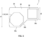
- FIG. 3 is a diagram illustrating configuration of an example of a second surface 3B of the toner sensor 3 according to the present embodiment.
- the second surface 3B is a surface opposite to the first surface 3A.
- the toner sensor 3 includes a substrate 30, planer coils 4, and interconnection patterns 5 (5A and 5B).
- the planer coils 4 include a first drive coil 41, a second drive coil 42, a first differential coil 43, and a second differential coil 44.
- a plurality of electronic components 6 are provided in either one of the interconnection patterns 5 (see FIG. 9 ).
- the substrate 30 has a rectangular shape with a cut across one corner thereof as shown in FIGS. 2 and 3 .
- the substrate 30 includes: a first section 30a having a first length d1 in a vertical direction, that is, a short side direction of the substrate 30; a second section 30b that is continuous from the first section 30a and has a graduated diminishing length in the vertical direction; and a third section 30c that is continuous from the second section 30b and has a second length d2 shorter than the first length d1 in the vertical direction.
- the planer coils 4 are disposed over the first section 30a and the second section 30b.
- the interconnection patterns 5 are disposed in the third section 30c.
- the planer coils 4 are disposed near one end of the substrate 30 in a long side direction, specifically, near an end not involving the cut in the long side direction.
- the interconnection patterns 5 are located near the other end of the substrate 30 in the long side direction, specifically, near an end involving the cut in the long side direction.
- the planer coils 4 are preferably disposed near an end involving the cut (hereinafter, referred to as "cut-involving end in the short side direction”.
- the interconnection patterns 5 may be located over the third section 30c and the second section 30b.
- the first drive coil 41 and the first differential coil 43 are disposed at a side of the first surface 3A over the first section 30a and the second section 30b.
- the first interconnection pattern 5A is disposed on the first surface 3A in the third section 30c.
- the first interconnection pattern 5A allows the first differential coil 43 to serve as a reference coil and the second differential coil 44 on the second surface 3B to serve as a sensing coil.
- the specified electronic elements 6 provided in the first interconnection pattern 5A enable a circuit of the toner sensor 3 based on the first interconnection pattern 5A (hereinafter, referred to as "first sensor circuit").
- the first differential coil 43 serves as a reference coil
- the second differential coil 44 serves as a sensing coil.
- the first surface 3A having the electronic elements 6 is a reference surface.
- the second surface 3B having no electronic elements 6 is a sensing surface.
- the second drive coil 42 and the second differential coil 44 are disposed at a side of the second surface 3B over the first section 30a and the second section 30b.
- the second interconnection pattern 5B is disposed on the second surface 3B in the third section 30c.
- the second interconnection pattern 5B allows the second differential coil 44 to serve as a reference coil and the first differential coil 43 to serve as a sensing coil.
- the specified electronic elements 6 provided in the second interconnection pattern 5B enable a circuit of the toner sensor 3 based on the second interconnection pattern 5B (hereinafter, referred to as "second sensor circuit").
- the second differential coil 44 serves as a reference coil
- the first differential coil 43 serves as a sensing coil.
- the second surface 3B having the electronic elements 6 is a reference surface.
- the first surface 3A having no electronic elements 6 is a sensing surface.
- Either the first surface 3A or the second surface 3B can be used as a sensing surface by selecting either the interconnection pattern 5A or the interconnection pattern 5B in the toner sensor 3 according to the present embodiment. That is, both the first surface 3A and the second surface 3B can be used as a reference surface or a sensing surface in the toner sensor 3 according to the present embodiment.
- the shape of the substrate 30 in a view from the side of the first surface 3A and the shape of the substrate 30 in a view from the side of the second surface 3B are different.
- the positional relationship between the planer coils 4 and the third section 30c is also different in the substrate 30 seen from the side of the first surface 3A than in the substrate 30 seen from the side of the second surface 3B.
- the toner sensor 3 When the toner sensor 3 is to be attached to a developing device in such a manner that the second surface 3B serves as a sensing surface, for example, the third section 30c may obstruct the planer coils 4 from being in an appropriate position and an appropriate orientation.
- the toner sensor 3 can be attached to the developing device in such a manner that the first surface 3A serves as a sensing surface to change the position of the third section 30c relative to the planer coils 4, and thus the planer coils 4 can be in the appropriate position and orientation.
- FIG. 4 is a circuit diagram illustrating an example of the toner sensor 3 according to the present embodiment.
- the sensor circuit (the first sensor circuit or the second sensor circuit) includes four coils (a first coil 4A, a second coil 4B, a third coil 4C, and a fourth coil 4D), an oscillation circuit 71, an amplifier circuit 72, a resistor 73, and a capacitor 74.
- the first coil 4A and the second coil 4B are drive coils.
- the third coil 4C is a reference coil.
- the fourth coil 4D is a sensing coil.
- the four coils (the first coil 4A, the second coil 4B, the third coil 4C, and the fourth coil 4D) shown in the circuit diagram correspond to the four planer coils 4 (the first drive coil 41, the second drive coil 42, the first differential coil 43, and the second differential coil 44) in the toner sensor 3.
- FIG. 4 is representing the circuit configuration of the first sensor circuit
- the first coil 4A corresponds to the first drive coil 41
- the second coil 4B corresponds to the second drive coil 42
- the third coil 4C corresponds to the first differential coil 43
- the fourth coil 4D corresponds to the second differential coil 44.
- FIG. 4 is representing the circuit configuration of the first sensor circuit
- the first coil 4A corresponds to the first drive coil 41
- the second coil 4B corresponds to the second drive coil 42
- the third coil 4C corresponds to the first differential coil 43
- the fourth coil 4D corresponds to the second differential coil 44.
- the first coil 4A corresponds to the second drive coil 42
- the second coil 4B corresponds to the first drive coil 41
- the third coil 4C corresponds to the second differential coil 44
- the fourth coil 4D corresponds to the first differential coil 43.
- the oscillation circuit 71 generates a high-frequency drive current that drives the first coil 4A and the second coil 4B.
- the first coil 4A and the second coil 4B are connected in series. Specifically, one end of the first coil 4A and one end of the second coil 4B are connected so that the magnetic flux generated through the first coil 4A and the magnetic flux generated through the second coil 4B are in the same direction when the drive current flows through the first coil 4A and the second coil 4B.
- the other end of the first coil 4A and the other end of the second coil 4B are connected to the oscillation circuit 71.
- the third coil 4C is magnetically coupled to the first coil 4A.
- the fourth coil 4D is magnetically coupled to the second coil 4B.
- One end of the third coil 4C and one end of the fourth coil 4D are differentially connected in series.
- one end of the third coil 4C and one end of the fourth coil 4D are connected so that the magnetic flux generated through the third coil 4C and the magnetic flux generated through the fourth coil 4D are in opposite directions when the drive current flows through the third coil 4C and the fourth coil 4D.
- a differential voltage V0 is input to the amplifier circuit 72.
- the differential voltage V0 is a voltage calculated by subtracting an induced voltage V2 in the fourth coil 4D from an induced voltage V1 in the third coil 4C.
- the other end of the third coil 4C is connected to the amplifier circuit 72 via the resistor 73.
- the resistor 73 is connected to a base of a bipolar transistor in the amplifier circuit 72 to be used for setting the amplification factor of the amplifier circuit 72.
- the other end of the fourth coil 4D is connected to the amplifier circuit 72 via the capacitor 74.
- the capacitor 74 has a function of removing a DC component of the differential voltage V0. Thus, an AC component of the differential voltage V0 is input to the amplifier circuit 72.
- the induced voltage V1 is generated in the third coil 4C, and the induced voltage V2 is generated in the fourth coil 4D.
- the induced voltage V2 is greater than the induced voltage VI, and therefore the differential voltage V0 is not 0 V.
- the differential voltage V0 is amplified in the amplifier circuit 72, and a signal is output from the amplifier circuit 72. The remaining toner amount is sensed using the signal.
- the toner sensor 3 may further include a selection section that zeroes the differential transformer.
- the selection section is disposed in a part of the first section 30a where the planer coil 4 is not present, for example.
- the selection section functions to adjust the value of the induced voltage V2 when no toner is present to a value equal to or greater than the induced voltage V1 for both the first sensor circuit and the second sensor circuit.
- the first sensor circuit and the second sensor circuit are enabled to provide an output that increases with increase in the remaining toner amount.
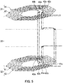
- FIG. 5 is a diagram illustrating configuration of an example of the planer coils 4 disposed in the toner sensor 3 according to the present embodiment.
- FIG. 6 is a cross sectional view of a part of the toner sensor 3 according to the present embodiment where the coils are disposed. In the present embodiment, the part where the coils are disposed is the first section 30a and the second section 30b of the substrate 30.
- the substrate 30 has a multi-layer structure including a first coil layer 31 at the side of the second surface 3B, a second coil layer 32 at the side of the first surface 3A, and an insulating layer 33.
- the insulating layer 33 is disposed between the first coil layer 31 and the second coil layer 32.
- the second drive coil 42 and the second differential coil 44 are disposed in the first coil layer 31.
- the second drive coil 42 is formed from a wire 42a wound into an octagonal shape.
- the second differential coil 44 is formed from a wire 44a wound into an octagonal shape.
- the wire 42a forming the second drive coil 42 and the wire 44a forming the second differential coil 44 are wound in parallel in the same direction.
- the first drive coil 41 and the first differential coil 43 are disposed in the second coil layer 32.
- the first drive coil 41 is formed from a wire 41a wound into an octagonal shape.
- the first differential coil 43 is formed from a wire 43a wound into an octagonal shape.
- the wire 41a forming the first drive coil 41 and the wire 43a forming the first differential coil 43 are wound in parallel in the same direction.
- the first drive coil 41 and the second drive coil 42 are electrically connected so that the flow of the drive current through the first drive coil 41 and the flow of the drive current through the second drive coil 42 are in the same direction.
- the first differential coil 43 and the second differential coil 44 are electrically connected so that the flow of the induced current in the first differential coil 43 and the flow of the induced current in the second differential coil 44 are in opposite directions.
- FIG. 7 is a first perspective view of the first developing device 2A.
- FIG. 8 is a second perspective view of the first developing device 2A.
- FIG. 9 is an enlarged view of a side of the first developing device 2A where the sensor is attached.
- the first perspective view is a top front view of the first developing device 2A.
- the second perspective view is a top rear view of the first developing device 2A. The shape of the first developing device 2A and the manner of the attachment of the toner sensor 3 to the first developing device 2A will be described with reference to FIGS. 7-9 .
- the first developing device 2A has a shape elongated in front and rear directions.
- the first developing device 2A includes a front wall 21 and a rear wall 22 at opposite ends in the front and rear directions.
- the front wall 21 and the rear wall 22 are parts of a housing 20 of the first developing device 2A.
- a developing roller 23 is disposed at a left side of the first developing device 2A.
- a toner containing section 24 that contains a toner is disposed at a right side of the first developing device 2A.
- a drive mechanism 25 that drives the developing roller 23, a stirring roller within the housing 20, and the like is disposed in the rear wall 22 of the first developing device 2A.
- the front wall 21 of the first developing device 2A has a rectangular shape with a cut across a corner, specifically, across a lower left corner when seen from the front. That is, the right side, which is the side where the toner containing section 24 is disposed, of the front wall 21 has a length in upward and downward directions longer than the left side, which is the side where the developing roller 23 is disposed, of the front wall 21.
- the toner sensor 3 is attached to the first developing device 2A having the above-described configuration as follows. That is, the toner sensor 3 is attached to the front wall 21 of the first developing device 2A in such a manner that: the second surface 3B serves as a sensing surface; the first section 30a is disposed at the right side of the first developing device 2A, that is, at the side where the toner containing section 24 is disposed; the cut-involving end in the short side direction is at the bottom; and the sensing surface faces the first developing device 2A.
- the sensing coil is disposed close to the toner containing section 24 and in the lowest possible position to be capable of high-accuracy sensing.
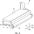
- FIG. 10 is a perspective view of the second developing device 2B.
- the perspective view as FIG. 10 is a top front view of the second developing device 2B.
- the shape of the second developing device 2B and the manner of the attachment of the toner sensor 3 to the second developing device 2B will be described with reference to FIG. 10 .
- the second developing device 2B has a shape elongated in the front and rear directions, and includes the front wall 21 and the rear wall 22 at opposite ends in the front and rear directions.
- the developing roller 23 is disposed at the right side of the second developing device 2B, and the toner containing section 24 is disposed at the left side of the second developing device 2B. That is, the positions of the developing roller 23 and the toner containing section 24 in the case of the second developing device 2B are opposite to the positions of the developing roller 23 and the toner containing section 24 in the case of the first developing device 2A.
- the drive mechanism 25, not shown in FIG. 10 that drives the developing roller 23, the magnetic roller, and the like is disposed in the rear wall 22 of the second developing device 2B.
- the front wall 21 of the second developing device 2B has a rectangular shape with a cut across a corner, specifically, across a lower right corner when seen from the front. That is, the left side, which is the side where the toner containing section 24 is disposed, of the front wall 21 has a length in the upward and downward directions longer than the right side, which is the side where the developing roller 23 is disposed, of the front wall 21. As described above, the shape of the front wall 21 of the second developing device 2B is different from the shape of the front wall 21 of the first developing device 2A.
- the third section 30c obstructs the sensing coil from being in an appropriate position and an appropriate orientation.
- the toner sensor 3 is attached to the second developing device 2B having the above-described configuration as follows. That is, the toner sensor 3 is attached to the front wall 21 of the second developing device 2B in such a manner that: the first surface 3A serves as a sensing surface; the first section 30a is disposed at the left side of the second developing device 2B, that is, at the side where the toner containing section 24 is disposed; the cut-involving end in the short side direction is at the bottom; and the sensing surface faces the second developing device 2B.
- the sensing coil is disposed close to the toner containing section 24 and in the lowest possible position to be capable of high-accuracy sensing.
- FIG. 11 is a diagram illustrating configuration of the planer coils 4 disposed in the toner sensor 3 according to a variation.
- FIG. 12 is a cross sectional view of a part of the toner sensor 3 according to the variation where the coils are disposed. The configuration of the planer coils 4 disposed in the toner sensor 3 according to the variation will be described with reference to FIGS. 11 and 12 .
- the substrate 30 includes two first coil layers 31 (a first coil layer 31a and a first coil layer 31b), two second coil layers 32 (a second coil layer 32a and a second coil layer 32b), and three insulating layers 33 (an upper insulating layer 33a, a middle insulating layer 33b, and a lower insulating layer 33c).
- the first coil layer 31a has substantially the same configuration as the first coil layer 31 shown in FIG. 5 .
- the second coil layer 32a has substantially the same configuration as the second coil layer 32 shown in FIG. 5 .
- the first coil layer 31b is formed between the upper insulating layer 33a and the middle insulating layer 33b.
- the second drive coil 42 and the second differential coil 44 are disposed in the first coil layer 31b.
- the second drive coil 42 and the second differential coil 44 are formed from the wire 42a and the wire 44a, respectively, each wound into an octagonal shape.
- the wire 42a forming the second drive coil 42 and the wire 44a forming the second differential coil 44 are wound in parallel in the same direction. In the variation, the direction of winding the wires 42a and 44a is different in the first coil layer 31a than in the first coil layer 31b.
- the second coil layer 32b is formed between the lower insulating layer 33c and the middle insulating layer 33b.
- the first drive coil 41 and the first differential coil 43 are disposed in the second coil layer 32b.
- the first drive coil 41 and the first differential coil 43 are formed from the wire 41a and the wire 43a, respectively, each wound into an octagonal shape.
- the wire 41a forming the first drive coil 41 and the wire 43a forming the first differential coil 43 are wound in parallel in the same direction. In the variation, the direction of winding the wires 41a and 43a is different in the second coil layer 32a than in the second coil layer 32b.
- the structure of the planer coils 4 disposed on the substrate 30 is not limited to the two-layer structure having the two coil layers 31 and 32 as shown in FIG. 6 but may be the four-layer structure having the four coil layers 31a, 31b, 32a, and 32b as shown in FIG. 11 .
- a multi-layer structure having five or more coil layers may be employed.
- the present embodiment provides the toner sensor 3 in which both the first surface 3A and the second surface 3B can be used as a reference surface or a sensing surface. Which of the first surface 3A and the second surface 3B should serve as a sensing surface for attaching the toner sensor 3 to the developing device 2 can be selected according to the shape of a part of the developing device 2 where the toner sensor 3 is attached. Thus, the toner sensor 3 can be attached to developing devices in various shapes in such a manner that the sensing coil is disposed in an appropriate position and an appropriate orientation.
- one coil layer may include one planer coil 4, although one coil layer includes two planer coils 4 according to the embodiment.
- the coil layer 31a may include the second differential coil 44
- the coil layer 31b may include the second drive coil 42
- the coil layer 32b may include the first drive coil 41
- the coil layer 32a may include the first differential coil 43.
- the differential transformer magnetic permeability sensor is not limited to the toner sensor 3 and may be a sensor for sensing the amount, the mixing ratio, or the like of any substances other than toner, although the toner sensor 3 has been described as an example of the differential transformer magnetic permeability sensor in the embodiment.
Landscapes
- Physics & Mathematics (AREA)
- General Physics & Mathematics (AREA)
- Condensed Matter Physics & Semiconductors (AREA)
- Chemical & Material Sciences (AREA)
- Health & Medical Sciences (AREA)
- Electrochemistry (AREA)
- Chemical Kinetics & Catalysis (AREA)
- Life Sciences & Earth Sciences (AREA)
- Analytical Chemistry (AREA)
- Biochemistry (AREA)
- General Health & Medical Sciences (AREA)
- Immunology (AREA)
- Pathology (AREA)
- Dry Development In Electrophotography (AREA)
- Investigating Or Analyzing Materials By The Use Of Magnetic Means (AREA)
Claims (9)
- Differentialtransformator-Magnetische-Permeabilität-Sensor (3) aufweisend:ein Substrat (30);mindestens eine Treiberspule (41, 42);eine Mehrzahl an elektronischen Komponenten (6), welche einen Schwingkreis aufweisen, der mit der mindestens einer Treiberspule verbunden ist und einen Treiberstrom erzeugt, der an die mindestens eine Treiberspule anzulegen ist;eine erste Differentialspule (43), welche an einer Seite einer ersten Fläche (3A) des Substrats angeordnet ist, und in welcher eine induzierte Spannung erzeugt wird, wenn die mindestens eine Treiberspule durch den Treiberstrom angetrieben wird;eine zweite Differentialspule (44), welche auf einer Seite einer zweiten Fläche (3B) gegenüber der ersten Fläche des Substrats angeordnet und mit der ersten Differentialspule verbunden ist, und in welcher eine induzierte Spannung erzeugt wird, wenn die mindestens eine Treiberspule durch den Treiberstrom angetrieben wird;ein erstes Zwischenverbindungsmuster (5A), das sich auf der ersten Fläche befindet und es ermöglicht, dass die erste Differentialspule als Referenzspule und die zweite Differentialspule als Sensorspule dient; undein zweites Zwischenverbindungsmuster (5B), das sich auf der zweiten Fläche befindet und es ermöglicht, dass die zweite Differentialspule als Referenzspule und die erste Differentialspule als Sensorspule dient, wobeidie elektronischen Komponenten entweder im ersten Zwischenverbindungsmuster oder im zweiten Zwischenverbindungsmuster bereitgestellt werden,die elektronischen Komponenten (6) in dem ersten Zwischenverbindungsmuster bereitgestellt werden, aber nicht in dem zweiten Zwischenverbindungsmuster bereitgestellt werden, um eine Schaltung auf Grundlage des ersten Zwischenverbindungsmuster zu ermöglichen, in welcher die erste Differentialspule als Referenzspule und die zweite Differentialspule als Sensorspule dient, unddie elektronischen Komponenten im zweiten Zwischenverbindungsmuster bereitgestellt werden, aber nicht im ersten Zwischenverbindungsmuster bereitgestellt werden, um eine Schaltung auf Grundlage des zweiten Zwischenverbindungsmuster zu ermöglichen, bei der die zweite Differentialspule als Referenzspule und die erste Differentialspule als Sensorspule dient.
- Differentialtransformator-Magnetische-Permeabilität-Sensor nach Anspruch 1, wobei
die erste Differentialspule und die zweite Differentialspule, bezüglich der Längsrichtung des Substrats, in der Nähe eines Endes des Substrats angeordnet sind,
das erste Zwischenverbindungsmuster und das zweite Zwischenverbindungsmuster, bezüglich der Längsrichtung des Substrats, in der Nähe des anderen Endes des Substrats angeordnet sind, und
eine Form des Substrats an dem einen Ende anders ist als eine Form des Substrats an dem anderen Ende. - Differentialtransformator-Magnetische-Permeabilität-Sensor nach Anspruch 2, wobei
das Substrat eine allgemein rechteckige Form hat, mit einem Schnitt quer über eine Ecke dieser, und
eine Länge des Substrats bezüglich einer Kurzseite-Richtung des Substrats an dem einen Ende länger ist als eine Länge des Substrats bezüglich einer Kurzseite-Richtung des Substrats an dem anderen Ende. - Differentialtransformator-Magnetische-Permeabilität-Sensor nach irgendeinem der Ansprüche 1 bis 3, wobei
die mindestens eine Treiberspule eine erste Treiberspule enthält, die auf der Seite der ersten Fläche angeordnet ist, und eine zweite Treiberspule, die auf der Seite der zweiten Fläche angeordnet ist und mit der ersten Treiberspule verbunden ist,
die induzierte Spannung in der ersten Differentialspule erzeugt wird, wenn die erste Treiberspule angetrieben wird, und
die induzierte Spannung in der zweiten Differentialspule erzeugt wird, wenn die zweite Treiberspule angetrieben wird. - Differentialtransformator-Magnetische-Permeabilität-Sensor nach Anspruch 4, wobei
das Substrat eine Mehrschicht-Struktur hat,
die erste Treiberspule und die erste Differentialspule in einer oder mehreren Schichten der Mehrschicht-Struktur angeordnet sind, die sich auf der Seite der ersten Fläche des Substrats befinden, und
die zweite Treiberspule und die zweite Differentialspule in einer oder mehreren Schichten der Mehrschicht-Struktur angeordnet sind, die sich auf der Seite der zweiten Fläche des Substrats befinden. - Differentialtransformator-Magnetische-Permeabilität-Sensor nach Anspruch 5, wobei
die erste Treiberspule und die erste Differentialspule in der gleichen Schicht angeordnet sind, von der einen oder mehreren Schichten, die sich auf der Seite der ersten Fläche des Substrats befinden, und
die zweite Treiberspule und die zweite Differentialspule in der gleichen Schicht angeordnet sind, von der einen oder mehreren Schichten, die sich auf der Seite der zweiten Fläche des Substrats befinden. - Differentialtransformator-Magnetische-Permeabilität-Sensor nach Anspruch 5, wobei
die erste Treiberspule und die erste Differentialspule in verschiedenen Schichten angeordnet sind, von der einen oder mehreren Schichten, die sich auf der Seite der ersten Fläche des Substrats befinden, und
die zweite Treiberspule und die zweite Differentialspule in verschiedenen Schichten angeordnet sind, von der einen oder mehreren Schichten, die sich auf der Seite der zweiten Fläche des Substrats befinden. - Differentialtransformator-Magnetische-Permeabilität-Sensor nach irgendeinem der Ansprüche 4 bis 7, wobei
die erste Treiberspule aus einem ersten Treiberdraht gebildet wird, welcher in einer Richtung gewickelt ist,
die erste Differentialspule aus einem ersten Differentialdraht gebildet wird, welcher in einer Richtung gewickelt ist,
der erste Treiberdraht und der erste Differentialdraht parallel in der gleichen Richtung gewickelt sind,
die zweite Treiberspule aus einem zweiten Treiberdraht gebildet wird, welcher in einer Richtung gewickelt ist,
die zweite Differentialspule aus einem zweiten Differentialdraht gebildet wird, welcher in einer Richtung gewickelt ist und
der zweite Treiberdraht und der zweite Differentialdraht parallel in der gleichen Richtung gewickelt sind. - Differentialtransformator-Magnetische-Permeabilität-Sensor nach irgendeinem der Ansprüche 1 bis 8, wobei
das Substrat aufweisteinen Spulenbereich, in dem die mindestens eine Treiberspule, die erste Differentialspule und die zweite Differentialspule angeordnet sind, undeinen Zwischenverbindungsmusterbereich, in dem das erste Zwischenverbindungsmuster und das zweite Zwischenverbindungsmuster angeordnet sind, wobei der Spulenbereich und der Zwischenverbindungsmusterbereich unterschiedliche Bereiche sind.
Applications Claiming Priority (1)
| Application Number | Priority Date | Filing Date | Title |
|---|---|---|---|
| JP2014071663A JP6050778B2 (ja) | 2014-03-31 | 2014-03-31 | 差動トランス式透磁率センサー |
Publications (2)
| Publication Number | Publication Date |
|---|---|
| EP2927751A1 EP2927751A1 (de) | 2015-10-07 |
| EP2927751B1 true EP2927751B1 (de) | 2020-09-30 |
Family
ID=52780423
Family Applications (1)
| Application Number | Title | Priority Date | Filing Date |
|---|---|---|---|
| EP15160801.5A Not-in-force EP2927751B1 (de) | 2014-03-31 | 2015-03-25 | Sensor für magnetische permeabilität für differentialtransformator |
Country Status (4)
| Country | Link |
|---|---|
| US (1) | US9632453B2 (de) |
| EP (1) | EP2927751B1 (de) |
| JP (1) | JP6050778B2 (de) |
| CN (1) | CN104950637B (de) |
Families Citing this family (3)
| Publication number | Priority date | Publication date | Assignee | Title |
|---|---|---|---|---|
| JP6565870B2 (ja) * | 2016-11-11 | 2019-08-28 | 京セラドキュメントソリューションズ株式会社 | 差動トランス式透磁率センサー |
| WO2020095354A1 (ja) * | 2018-11-06 | 2020-05-14 | 株式会社島津製作所 | 磁性体検査装置および磁性体検査システム |
| JP7269838B2 (ja) * | 2019-09-02 | 2023-05-09 | 株式会社日立製作所 | 応力分布計測装置および応力分布計測方法 |
Family Cites Families (10)
| Publication number | Priority date | Publication date | Assignee | Title |
|---|---|---|---|---|
| KR100468833B1 (ko) * | 1998-07-28 | 2005-03-16 | 삼성전자주식회사 | 차동스파이어럴형자계검출소자및이를채용한자계검출모듈 |
| JP2000131406A (ja) * | 1998-10-20 | 2000-05-12 | Tdk Corp | 差動トランス、磁気的センサ及び磁気的検知装置 |
| JP2001099654A (ja) * | 1999-10-04 | 2001-04-13 | Alps Electric Co Ltd | フラックスゲートセンサ及びその製造方法 |
| JP2001165910A (ja) | 1999-12-10 | 2001-06-22 | Tdk Corp | 磁気センサ |
| US6642711B2 (en) * | 2001-01-24 | 2003-11-04 | Texas Instruments Incorporated | Digital inductive position sensor |
| US20060132123A1 (en) * | 2004-12-22 | 2006-06-22 | General Electric Company | Eddy current array probes with enhanced drive fields |
| KR100836767B1 (ko) * | 2007-02-05 | 2008-06-10 | 삼성전자주식회사 | 높은 전압을 제어하는 모스 트랜지스터를 포함하는 반도체소자 및 그 형성 방법 |
| CN101788259B (zh) * | 2010-03-04 | 2012-09-05 | 上海雷尼威尔测量技术有限公司 | 双丝差动型磁致伸缩位移传感器 |
| KR101414102B1 (ko) * | 2011-10-20 | 2014-07-01 | 교세라 도큐멘트 솔루션즈 가부시키가이샤 | 차동 변압기식 자기 센서 |
| JP5830450B2 (ja) * | 2011-10-20 | 2015-12-09 | 京セラドキュメントソリューションズ株式会社 | 差動トランス式磁気センサー |
-
2014
- 2014-03-31 JP JP2014071663A patent/JP6050778B2/ja not_active Expired - Fee Related
-
2015
- 2015-03-25 EP EP15160801.5A patent/EP2927751B1/de not_active Not-in-force
- 2015-03-26 CN CN201510135982.XA patent/CN104950637B/zh not_active Expired - Fee Related
- 2015-03-26 US US14/669,543 patent/US9632453B2/en active Active
Non-Patent Citations (1)
| Title |
|---|
| None * |
Also Published As
| Publication number | Publication date |
|---|---|
| EP2927751A1 (de) | 2015-10-07 |
| JP6050778B2 (ja) | 2016-12-21 |
| CN104950637B (zh) | 2019-03-15 |
| US20150277280A1 (en) | 2015-10-01 |
| CN104950637A (zh) | 2015-09-30 |
| US9632453B2 (en) | 2017-04-25 |
| JP2015194364A (ja) | 2015-11-05 |
Similar Documents
| Publication | Publication Date | Title |
|---|---|---|
| JP5690795B2 (ja) | 画像形成装置 | |
| JP2016065849A (ja) | 媒体サイズ検知装置及び画像処理装置 | |
| US9632453B2 (en) | Differential transformer magnetic permeability sensor | |
| CN103063235B (zh) | 差动变压器式磁传感器 | |
| CN103712636B (zh) | 差动变压器式磁传感器及图像形成装置 | |
| JP5820795B2 (ja) | 画像形成装置 | |
| JP5865813B2 (ja) | 差動トランス式磁気センサー | |
| JP6331269B2 (ja) | 透磁率検知器、現像装置、画像形成装置 | |
| JP5830450B2 (ja) | 差動トランス式磁気センサー | |
| US9671735B2 (en) | Differential transformer magnetic permeability sensor | |
| JP5696120B2 (ja) | 画像形成装置 | |
| JP5768000B2 (ja) | 差動トランス式磁気センサー及び画像形成装置 | |
| JP6295970B2 (ja) | 給紙装置、及びそれを備える画像形成装置 |
Legal Events
| Date | Code | Title | Description |
|---|---|---|---|
| PUAI | Public reference made under article 153(3) epc to a published international application that has entered the european phase |
Free format text: ORIGINAL CODE: 0009012 |
|
| AK | Designated contracting states |
Kind code of ref document: A1 Designated state(s): AL AT BE BG CH CY CZ DE DK EE ES FI FR GB GR HR HU IE IS IT LI LT LU LV MC MK MT NL NO PL PT RO RS SE SI SK SM TR |
|
| AX | Request for extension of the european patent |
Extension state: BA ME |
|
| 17P | Request for examination filed |
Effective date: 20160405 |
|
| RBV | Designated contracting states (corrected) |
Designated state(s): AL AT BE BG CH CY CZ DE DK EE ES FI FR GB GR HR HU IE IS IT LI LT LU LV MC MK MT NL NO PL PT RO RS SE SI SK SM TR |
|
| STAA | Information on the status of an ep patent application or granted ep patent |
Free format text: STATUS: EXAMINATION IS IN PROGRESS |
|
| 17Q | First examination report despatched |
Effective date: 20181122 |
|
| GRAP | Despatch of communication of intention to grant a patent |
Free format text: ORIGINAL CODE: EPIDOSNIGR1 |
|
| STAA | Information on the status of an ep patent application or granted ep patent |
Free format text: STATUS: GRANT OF PATENT IS INTENDED |
|
| INTG | Intention to grant announced |
Effective date: 20200421 |
|
| RIN1 | Information on inventor provided before grant (corrected) |
Inventor name: AIKAWA, YUKIHIRO |
|
| GRAS | Grant fee paid |
Free format text: ORIGINAL CODE: EPIDOSNIGR3 |
|
| GRAA | (expected) grant |
Free format text: ORIGINAL CODE: 0009210 |
|
| STAA | Information on the status of an ep patent application or granted ep patent |
Free format text: STATUS: THE PATENT HAS BEEN GRANTED |
|
| AK | Designated contracting states |
Kind code of ref document: B1 Designated state(s): AL AT BE BG CH CY CZ DE DK EE ES FI FR GB GR HR HU IE IS IT LI LT LU LV MC MK MT NL NO PL PT RO RS SE SI SK SM TR |
|
| REG | Reference to a national code |
Ref country code: CH Ref legal event code: EP Ref country code: GB Ref legal event code: FG4D |
|
| REG | Reference to a national code |
Ref country code: DE Ref legal event code: R096 Ref document number: 602015059723 Country of ref document: DE Ref country code: AT Ref legal event code: REF Ref document number: 1319436 Country of ref document: AT Kind code of ref document: T Effective date: 20201015 |
|
| REG | Reference to a national code |
Ref country code: IE Ref legal event code: FG4D |
|
| PG25 | Lapsed in a contracting state [announced via postgrant information from national office to epo] |
Ref country code: NO Free format text: LAPSE BECAUSE OF FAILURE TO SUBMIT A TRANSLATION OF THE DESCRIPTION OR TO PAY THE FEE WITHIN THE PRESCRIBED TIME-LIMIT Effective date: 20201230 Ref country code: GR Free format text: LAPSE BECAUSE OF FAILURE TO SUBMIT A TRANSLATION OF THE DESCRIPTION OR TO PAY THE FEE WITHIN THE PRESCRIBED TIME-LIMIT Effective date: 20201231 Ref country code: SE Free format text: LAPSE BECAUSE OF FAILURE TO SUBMIT A TRANSLATION OF THE DESCRIPTION OR TO PAY THE FEE WITHIN THE PRESCRIBED TIME-LIMIT Effective date: 20200930 Ref country code: BG Free format text: LAPSE BECAUSE OF FAILURE TO SUBMIT A TRANSLATION OF THE DESCRIPTION OR TO PAY THE FEE WITHIN THE PRESCRIBED TIME-LIMIT Effective date: 20201230 Ref country code: HR Free format text: LAPSE BECAUSE OF FAILURE TO SUBMIT A TRANSLATION OF THE DESCRIPTION OR TO PAY THE FEE WITHIN THE PRESCRIBED TIME-LIMIT Effective date: 20200930 Ref country code: FI Free format text: LAPSE BECAUSE OF FAILURE TO SUBMIT A TRANSLATION OF THE DESCRIPTION OR TO PAY THE FEE WITHIN THE PRESCRIBED TIME-LIMIT Effective date: 20200930 |
|
| REG | Reference to a national code |
Ref country code: AT Ref legal event code: MK05 Ref document number: 1319436 Country of ref document: AT Kind code of ref document: T Effective date: 20200930 |
|
| PG25 | Lapsed in a contracting state [announced via postgrant information from national office to epo] |
Ref country code: LV Free format text: LAPSE BECAUSE OF FAILURE TO SUBMIT A TRANSLATION OF THE DESCRIPTION OR TO PAY THE FEE WITHIN THE PRESCRIBED TIME-LIMIT Effective date: 20200930 Ref country code: RS Free format text: LAPSE BECAUSE OF FAILURE TO SUBMIT A TRANSLATION OF THE DESCRIPTION OR TO PAY THE FEE WITHIN THE PRESCRIBED TIME-LIMIT Effective date: 20200930 |
|
| REG | Reference to a national code |
Ref country code: NL Ref legal event code: MP Effective date: 20200930 |
|
| REG | Reference to a national code |
Ref country code: LT Ref legal event code: MG4D |
|
| PG25 | Lapsed in a contracting state [announced via postgrant information from national office to epo] |
Ref country code: CZ Free format text: LAPSE BECAUSE OF FAILURE TO SUBMIT A TRANSLATION OF THE DESCRIPTION OR TO PAY THE FEE WITHIN THE PRESCRIBED TIME-LIMIT Effective date: 20200930 Ref country code: EE Free format text: LAPSE BECAUSE OF FAILURE TO SUBMIT A TRANSLATION OF THE DESCRIPTION OR TO PAY THE FEE WITHIN THE PRESCRIBED TIME-LIMIT Effective date: 20200930 Ref country code: RO Free format text: LAPSE BECAUSE OF FAILURE TO SUBMIT A TRANSLATION OF THE DESCRIPTION OR TO PAY THE FEE WITHIN THE PRESCRIBED TIME-LIMIT Effective date: 20200930 Ref country code: SM Free format text: LAPSE BECAUSE OF FAILURE TO SUBMIT A TRANSLATION OF THE DESCRIPTION OR TO PAY THE FEE WITHIN THE PRESCRIBED TIME-LIMIT Effective date: 20200930 Ref country code: LT Free format text: LAPSE BECAUSE OF FAILURE TO SUBMIT A TRANSLATION OF THE DESCRIPTION OR TO PAY THE FEE WITHIN THE PRESCRIBED TIME-LIMIT Effective date: 20200930 Ref country code: NL Free format text: LAPSE BECAUSE OF FAILURE TO SUBMIT A TRANSLATION OF THE DESCRIPTION OR TO PAY THE FEE WITHIN THE PRESCRIBED TIME-LIMIT Effective date: 20200930 Ref country code: PT Free format text: LAPSE BECAUSE OF FAILURE TO SUBMIT A TRANSLATION OF THE DESCRIPTION OR TO PAY THE FEE WITHIN THE PRESCRIBED TIME-LIMIT Effective date: 20210201 |
|
| PG25 | Lapsed in a contracting state [announced via postgrant information from national office to epo] |
Ref country code: ES Free format text: LAPSE BECAUSE OF FAILURE TO SUBMIT A TRANSLATION OF THE DESCRIPTION OR TO PAY THE FEE WITHIN THE PRESCRIBED TIME-LIMIT Effective date: 20200930 Ref country code: AL Free format text: LAPSE BECAUSE OF FAILURE TO SUBMIT A TRANSLATION OF THE DESCRIPTION OR TO PAY THE FEE WITHIN THE PRESCRIBED TIME-LIMIT Effective date: 20200930 Ref country code: AT Free format text: LAPSE BECAUSE OF FAILURE TO SUBMIT A TRANSLATION OF THE DESCRIPTION OR TO PAY THE FEE WITHIN THE PRESCRIBED TIME-LIMIT Effective date: 20200930 Ref country code: PL Free format text: LAPSE BECAUSE OF FAILURE TO SUBMIT A TRANSLATION OF THE DESCRIPTION OR TO PAY THE FEE WITHIN THE PRESCRIBED TIME-LIMIT Effective date: 20200930 Ref country code: IS Free format text: LAPSE BECAUSE OF FAILURE TO SUBMIT A TRANSLATION OF THE DESCRIPTION OR TO PAY THE FEE WITHIN THE PRESCRIBED TIME-LIMIT Effective date: 20210130 |
|
| PG25 | Lapsed in a contracting state [announced via postgrant information from national office to epo] |
Ref country code: SK Free format text: LAPSE BECAUSE OF FAILURE TO SUBMIT A TRANSLATION OF THE DESCRIPTION OR TO PAY THE FEE WITHIN THE PRESCRIBED TIME-LIMIT Effective date: 20200930 |
|
| REG | Reference to a national code |
Ref country code: DE Ref legal event code: R097 Ref document number: 602015059723 Country of ref document: DE |
|
| PLBE | No opposition filed within time limit |
Free format text: ORIGINAL CODE: 0009261 |
|
| STAA | Information on the status of an ep patent application or granted ep patent |
Free format text: STATUS: NO OPPOSITION FILED WITHIN TIME LIMIT |
|
| PG25 | Lapsed in a contracting state [announced via postgrant information from national office to epo] |
Ref country code: DK Free format text: LAPSE BECAUSE OF FAILURE TO SUBMIT A TRANSLATION OF THE DESCRIPTION OR TO PAY THE FEE WITHIN THE PRESCRIBED TIME-LIMIT Effective date: 20200930 |
|
| 26N | No opposition filed |
Effective date: 20210701 |
|
| PG25 | Lapsed in a contracting state [announced via postgrant information from national office to epo] |
Ref country code: MC Free format text: LAPSE BECAUSE OF FAILURE TO SUBMIT A TRANSLATION OF THE DESCRIPTION OR TO PAY THE FEE WITHIN THE PRESCRIBED TIME-LIMIT Effective date: 20200930 Ref country code: IT Free format text: LAPSE BECAUSE OF FAILURE TO SUBMIT A TRANSLATION OF THE DESCRIPTION OR TO PAY THE FEE WITHIN THE PRESCRIBED TIME-LIMIT Effective date: 20200930 |
|
| REG | Reference to a national code |
Ref country code: CH Ref legal event code: PL |
|
| GBPC | Gb: european patent ceased through non-payment of renewal fee |
Effective date: 20210325 |
|
| PG25 | Lapsed in a contracting state [announced via postgrant information from national office to epo] |
Ref country code: SI Free format text: LAPSE BECAUSE OF FAILURE TO SUBMIT A TRANSLATION OF THE DESCRIPTION OR TO PAY THE FEE WITHIN THE PRESCRIBED TIME-LIMIT Effective date: 20200930 |
|
| REG | Reference to a national code |
Ref country code: BE Ref legal event code: MM Effective date: 20210331 |
|
| PG25 | Lapsed in a contracting state [announced via postgrant information from national office to epo] |
Ref country code: GB Free format text: LAPSE BECAUSE OF NON-PAYMENT OF DUE FEES Effective date: 20210325 Ref country code: IE Free format text: LAPSE BECAUSE OF NON-PAYMENT OF DUE FEES Effective date: 20210325 Ref country code: FR Free format text: LAPSE BECAUSE OF NON-PAYMENT OF DUE FEES Effective date: 20210331 Ref country code: CH Free format text: LAPSE BECAUSE OF NON-PAYMENT OF DUE FEES Effective date: 20210331 Ref country code: LI Free format text: LAPSE BECAUSE OF NON-PAYMENT OF DUE FEES Effective date: 20210331 Ref country code: LU Free format text: LAPSE BECAUSE OF NON-PAYMENT OF DUE FEES Effective date: 20210325 |
|
| PG25 | Lapsed in a contracting state [announced via postgrant information from national office to epo] |
Ref country code: IS Free format text: LAPSE BECAUSE OF FAILURE TO SUBMIT A TRANSLATION OF THE DESCRIPTION OR TO PAY THE FEE WITHIN THE PRESCRIBED TIME-LIMIT Effective date: 20210130 |
|
| PG25 | Lapsed in a contracting state [announced via postgrant information from national office to epo] |
Ref country code: BE Free format text: LAPSE BECAUSE OF NON-PAYMENT OF DUE FEES Effective date: 20210331 |
|
| PG25 | Lapsed in a contracting state [announced via postgrant information from national office to epo] |
Ref country code: HU Free format text: LAPSE BECAUSE OF FAILURE TO SUBMIT A TRANSLATION OF THE DESCRIPTION OR TO PAY THE FEE WITHIN THE PRESCRIBED TIME-LIMIT; INVALID AB INITIO Effective date: 20150325 |
|
| PGFP | Annual fee paid to national office [announced via postgrant information from national office to epo] |
Ref country code: DE Payment date: 20230221 Year of fee payment: 9 |
|
| P01 | Opt-out of the competence of the unified patent court (upc) registered |
Effective date: 20230420 |
|
| PG25 | Lapsed in a contracting state [announced via postgrant information from national office to epo] |
Ref country code: CY Free format text: LAPSE BECAUSE OF FAILURE TO SUBMIT A TRANSLATION OF THE DESCRIPTION OR TO PAY THE FEE WITHIN THE PRESCRIBED TIME-LIMIT Effective date: 20200930 |
|
| PG25 | Lapsed in a contracting state [announced via postgrant information from national office to epo] |
Ref country code: MK Free format text: LAPSE BECAUSE OF FAILURE TO SUBMIT A TRANSLATION OF THE DESCRIPTION OR TO PAY THE FEE WITHIN THE PRESCRIBED TIME-LIMIT Effective date: 20200930 |
|
| PG25 | Lapsed in a contracting state [announced via postgrant information from national office to epo] |
Ref country code: MT Free format text: LAPSE BECAUSE OF FAILURE TO SUBMIT A TRANSLATION OF THE DESCRIPTION OR TO PAY THE FEE WITHIN THE PRESCRIBED TIME-LIMIT Effective date: 20200930 |
|
| REG | Reference to a national code |
Ref country code: DE Ref legal event code: R119 Ref document number: 602015059723 Country of ref document: DE |
|
| PG25 | Lapsed in a contracting state [announced via postgrant information from national office to epo] |
Ref country code: DE Free format text: LAPSE BECAUSE OF NON-PAYMENT OF DUE FEES Effective date: 20241001 |
|
| PG25 | Lapsed in a contracting state [announced via postgrant information from national office to epo] |
Ref country code: DE Free format text: LAPSE BECAUSE OF NON-PAYMENT OF DUE FEES Effective date: 20241001 |
|
| PG25 | Lapsed in a contracting state [announced via postgrant information from national office to epo] |
Ref country code: TR Free format text: LAPSE BECAUSE OF FAILURE TO SUBMIT A TRANSLATION OF THE DESCRIPTION OR TO PAY THE FEE WITHIN THE PRESCRIBED TIME-LIMIT Effective date: 20200930 |