EP2918402B1 - Optical device, head mounted display, assembling method for the same, holographic diffraction grating, display device, and alignment device - Google Patents
Optical device, head mounted display, assembling method for the same, holographic diffraction grating, display device, and alignment device Download PDFInfo
- Publication number
- EP2918402B1 EP2918402B1 EP15157880.4A EP15157880A EP2918402B1 EP 2918402 B1 EP2918402 B1 EP 2918402B1 EP 15157880 A EP15157880 A EP 15157880A EP 2918402 B1 EP2918402 B1 EP 2918402B1
- Authority
- EP
- European Patent Office
- Prior art keywords
- light
- diffraction grating
- light guide
- holographic diffraction
- alignment mark
- Prior art date
- Legal status (The legal status is an assumption and is not a legal conclusion. Google has not performed a legal analysis and makes no representation as to the accuracy of the status listed.)
- Not-in-force
Links
Images


Classifications
-
- G—PHYSICS
- G02—OPTICS
- G02B—OPTICAL ELEMENTS, SYSTEMS OR APPARATUS
- G02B27/00—Optical systems or apparatus not provided for by any of the groups G02B1/00 - G02B26/00, G02B30/00
- G02B27/01—Head-up displays
- G02B27/0101—Head-up displays characterised by optical features
-
- G—PHYSICS
- G02—OPTICS
- G02B—OPTICAL ELEMENTS, SYSTEMS OR APPARATUS
- G02B27/00—Optical systems or apparatus not provided for by any of the groups G02B1/00 - G02B26/00, G02B30/00
- G02B27/01—Head-up displays
- G02B27/017—Head mounted
- G02B27/0172—Head mounted characterised by optical features
-
- G—PHYSICS
- G02—OPTICS
- G02B—OPTICAL ELEMENTS, SYSTEMS OR APPARATUS
- G02B27/00—Optical systems or apparatus not provided for by any of the groups G02B1/00 - G02B26/00, G02B30/00
- G02B27/01—Head-up displays
- G02B27/017—Head mounted
-
- G—PHYSICS
- G02—OPTICS
- G02B—OPTICAL ELEMENTS, SYSTEMS OR APPARATUS
- G02B27/00—Optical systems or apparatus not provided for by any of the groups G02B1/00 - G02B26/00, G02B30/00
- G02B27/42—Diffraction optics, i.e. systems including a diffractive element being designed for providing a diffractive effect
- G02B27/4205—Diffraction optics, i.e. systems including a diffractive element being designed for providing a diffractive effect having a diffractive optical element [DOE] contributing to image formation, e.g. whereby modulation transfer function MTF or optical aberrations are relevant
-
- G—PHYSICS
- G02—OPTICS
- G02B—OPTICAL ELEMENTS, SYSTEMS OR APPARATUS
- G02B27/00—Optical systems or apparatus not provided for by any of the groups G02B1/00 - G02B26/00, G02B30/00
- G02B27/42—Diffraction optics, i.e. systems including a diffractive element being designed for providing a diffractive effect
- G02B27/4272—Diffraction optics, i.e. systems including a diffractive element being designed for providing a diffractive effect having plural diffractive elements positioned sequentially along the optical path
-
- G—PHYSICS
- G02—OPTICS
- G02B—OPTICAL ELEMENTS, SYSTEMS OR APPARATUS
- G02B27/00—Optical systems or apparatus not provided for by any of the groups G02B1/00 - G02B26/00, G02B30/00
- G02B27/42—Diffraction optics, i.e. systems including a diffractive element being designed for providing a diffractive effect
- G02B27/44—Grating systems; Zone plate systems
-
- G—PHYSICS
- G02—OPTICS
- G02B—OPTICAL ELEMENTS, SYSTEMS OR APPARATUS
- G02B5/00—Optical elements other than lenses
- G02B5/18—Diffraction gratings
-
- G—PHYSICS
- G02—OPTICS
- G02B—OPTICAL ELEMENTS, SYSTEMS OR APPARATUS
- G02B6/00—Light guides; Structural details of arrangements comprising light guides and other optical elements, e.g. couplings
- G02B6/24—Coupling light guides
- G02B6/26—Optical coupling means
- G02B6/34—Optical coupling means utilising prism or grating
-
- G—PHYSICS
- G02—OPTICS
- G02B—OPTICAL ELEMENTS, SYSTEMS OR APPARATUS
- G02B27/00—Optical systems or apparatus not provided for by any of the groups G02B1/00 - G02B26/00, G02B30/00
- G02B27/01—Head-up displays
- G02B27/017—Head mounted
- G02B2027/0178—Eyeglass type
-
- G—PHYSICS
- G02—OPTICS
- G02B—OPTICAL ELEMENTS, SYSTEMS OR APPARATUS
- G02B27/00—Optical systems or apparatus not provided for by any of the groups G02B1/00 - G02B26/00, G02B30/00
- G02B27/01—Head-up displays
- G02B2027/0192—Supplementary details
- G02B2027/0198—System for aligning or maintaining alignment of an image in a predetermined direction
Definitions
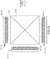
- the optical device 120 In order to assemble the optical device 120 having such a configuration and structure, it is necessary to precisely align the first holographic diffraction grating 131 and the second holographic diffraction grating 135 with each other. In particular, it is important to control and manage parallelism on an extending direction of first interference fringes formed in the first holographic diffraction grating 131 and an extending direction of second interference fringes formed in the second holographic diffraction grating 135.
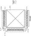
- the following form can be provided: in a state where the relative alignment of the first holographic diffraction grating and the second holographic diffraction grating is completed, the first A alignment mark and the second A alignment mark are disposed at positions where the first A alignment mark and the second A alignment mark do not overlap, and the first B alignment mark and the second B alignment mark are disposed at positions where the first B alignment mark and the second B alignment mark do not overlap.
- the first A alignment mark and the second A alignment mark are imaged by a first imaging device; and the first B alignment mark and the second B alignment mark are imaged by a second imaging device.
- the imaging device may be an imaging device having a well-known configuration and structure.
- the first holographic diffraction grating is disposed on a first surface of the light guide plate; and the second holographic diffraction grating is disposed on a second surface of the light guide plate, the second surface being opposed to the first surface.
- the term "semi-transmissive" is used in some cases. This term is used in not a meaning that 1/2 (50%) of incident light is transmitted or reflected, but a meaning that part of incident light is transmitted and the rest is reflected.
- the spatial light modulation device examples include a light valve, for example, a transmissive-type or reflection-type liquid crystal display device such as an LCOS (Liquid Crystal On Silicon), and a digital micromirror device (DMD).
- a light valve for example, a transmissive-type or reflection-type liquid crystal display device such as an LCOS (Liquid Crystal On Silicon), and a digital micromirror device (DMD).
- the light source include the light emitting elements described above.
- the reflection-type spatial light modulation device can include a liquid crystal display device and a polarizing beam splitter. The polarizing beam splitter reflects part of light from the light source and guides the light to the liquid crystal display device, and causes part of the light reflected by the liquid crystal display device to pass to guide the light to an optical system.
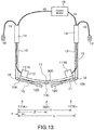
- each casing 113 may be detachably attached to the temple portion of the frame of the eyeglasses owned by the observer with the mounting member 19.
- Each casing 113 may be attached to the outer side of the temple portion 13 or to the inner side of the temple portion 13.
- the first holographic diffraction grating 131 and the second holographic diffraction grating 135 are relatively aligned with each other.
- the shapes of the first A alignment mark, the second A alignment mark, the first B alignment mark, and the second B alignment mark are prescribed, or the arrangement of those alignment marks is prescribed. So, the first holographic diffraction grating and the second holographic diffraction grating can be relatively aligned with each other certainly and easily based on a simplified method.
- an image forming device including, as shown in Fig. 21 as a conceptual diagram, light emitting panels 511R, 511G, and 511B on which light emitting elements 501R, 501G, and 501B are arranged in a two-dimensional matrix, respectively.
- Light beams output from the light emitting panels 511R, 511G, and 511B are input to a dichroic prism 503 and collected into one optical path.
- the passages/non-passages of the light beams output from the dichroic prism 503 are controlled by a light passage control device 504, and the light beams are input to the light guide plate 121 via the collimating optical system 112.
Landscapes
- Physics & Mathematics (AREA)
- General Physics & Mathematics (AREA)
- Optics & Photonics (AREA)
- Diffracting Gratings Or Hologram Optical Elements (AREA)
Applications Claiming Priority (1)
| Application Number | Priority Date | Filing Date | Title |
|---|---|---|---|
| JP2014052043A JP6201836B2 (ja) | 2014-03-14 | 2014-03-14 | 光学装置及びその組立方法、ホログラム回折格子、表示装置並びにアライメント装置 |
Publications (2)
| Publication Number | Publication Date |
|---|---|
| EP2918402A1 EP2918402A1 (en) | 2015-09-16 |
| EP2918402B1 true EP2918402B1 (en) | 2020-12-02 |
Family
ID=52630243
Family Applications (1)
| Application Number | Title | Priority Date | Filing Date |
|---|---|---|---|
| EP15157880.4A Not-in-force EP2918402B1 (en) | 2014-03-14 | 2015-03-05 | Optical device, head mounted display, assembling method for the same, holographic diffraction grating, display device, and alignment device |
Country Status (4)
| Country | Link |
|---|---|
| US (1) | US11073693B2 (https=) |
| EP (1) | EP2918402B1 (https=) |
| JP (1) | JP6201836B2 (https=) |
| CN (2) | CN110068927B (https=) |
Families Citing this family (119)
| Publication number | Priority date | Publication date | Assignee | Title |
|---|---|---|---|---|
| GB0522968D0 (en) | 2005-11-11 | 2005-12-21 | Popovich Milan M | Holographic illumination device |
| GB0718706D0 (en) | 2007-09-25 | 2007-11-07 | Creative Physics Ltd | Method and apparatus for reducing laser speckle |
| US9335604B2 (en) | 2013-12-11 | 2016-05-10 | Milan Momcilo Popovich | Holographic waveguide display |
| US11726332B2 (en) | 2009-04-27 | 2023-08-15 | Digilens Inc. | Diffractive projection apparatus |
| US11204540B2 (en) | 2009-10-09 | 2021-12-21 | Digilens Inc. | Diffractive waveguide providing a retinal image |
| US20200057353A1 (en) | 2009-10-09 | 2020-02-20 | Digilens Inc. | Compact Edge Illuminated Diffractive Display |
| US9274349B2 (en) | 2011-04-07 | 2016-03-01 | Digilens Inc. | Laser despeckler based on angular diversity |
| EP2748670B1 (en) | 2011-08-24 | 2015-11-18 | Rockwell Collins, Inc. | Wearable data display |
| WO2016020630A2 (en) | 2014-08-08 | 2016-02-11 | Milan Momcilo Popovich | Waveguide laser illuminator incorporating a despeckler |
| US10670876B2 (en) | 2011-08-24 | 2020-06-02 | Digilens Inc. | Waveguide laser illuminator incorporating a despeckler |
| JP5879973B2 (ja) | 2011-11-30 | 2016-03-08 | ソニー株式会社 | 光反射部材、光ビーム伸長装置、画像表示装置及び光学装置 |
| US20150010265A1 (en) | 2012-01-06 | 2015-01-08 | Milan, Momcilo POPOVICH | Contact image sensor using switchable bragg gratings |
| EP2808725B1 (en) | 2012-01-24 | 2018-09-26 | Sony Corporation | Head-mounted display device with a light-shielding member |
| EP2842003B1 (en) | 2012-04-25 | 2019-02-27 | Rockwell Collins, Inc. | Holographic wide angle display |
| JP6145966B2 (ja) | 2012-05-09 | 2017-06-14 | ソニー株式会社 | 表示装置 |
| US9456744B2 (en) | 2012-05-11 | 2016-10-04 | Digilens, Inc. | Apparatus for eye tracking |
| US9933684B2 (en) | 2012-11-16 | 2018-04-03 | Rockwell Collins, Inc. | Transparent waveguide display providing upper and lower fields of view having a specific light output aperture configuration |
| JP6123342B2 (ja) | 2013-02-20 | 2017-05-10 | ソニー株式会社 | 表示装置 |
| EP2985652A4 (en) | 2013-04-11 | 2016-12-14 | Sony Corp | IMAGE DISPLAY AND DISPLAY DEVICE |
| US10527859B2 (en) | 2013-04-11 | 2020-01-07 | Sony Corporation | Image display device and display apparatus |
| US10209517B2 (en) | 2013-05-20 | 2019-02-19 | Digilens, Inc. | Holographic waveguide eye tracker |
| WO2015001839A1 (ja) | 2013-07-04 | 2015-01-08 | ソニー株式会社 | 表示装置 |
| US9952435B2 (en) | 2013-07-16 | 2018-04-24 | Sony Corporation | Display apparatus having curved image forming apparatus |
| WO2015008530A1 (ja) | 2013-07-16 | 2015-01-22 | ソニー株式会社 | 表示装置 |
| US9727772B2 (en) | 2013-07-31 | 2017-08-08 | Digilens, Inc. | Method and apparatus for contact image sensing |
| JP6391952B2 (ja) | 2014-03-17 | 2018-09-19 | ソニー株式会社 | 表示装置及び光学装置 |
| JP2015184561A (ja) | 2014-03-25 | 2015-10-22 | ソニー株式会社 | 導光装置、画像表示装置及び表示装置 |
| JP2015184560A (ja) | 2014-03-25 | 2015-10-22 | ソニー株式会社 | 導光装置、画像表示装置及び表示装置 |
| US9465215B2 (en) * | 2014-03-28 | 2016-10-11 | Google Inc. | Lightguide with multiple in-coupling holograms for head wearable display |
| WO2016020632A1 (en) | 2014-08-08 | 2016-02-11 | Milan Momcilo Popovich | Method for holographic mastering and replication |
| WO2016042283A1 (en) | 2014-09-19 | 2016-03-24 | Milan Momcilo Popovich | Method and apparatus for generating input images for holographic waveguide displays |
| EP3198192A1 (en) | 2014-09-26 | 2017-08-02 | Milan Momcilo Popovich | Holographic waveguide opticaltracker |
| US9568789B2 (en) * | 2014-11-19 | 2017-02-14 | Omnivision Technologies, Inc. | Panel carrier for a liquid crystal on silicon panel and method for electrically interconnecting same |
| JP6690550B2 (ja) * | 2014-11-27 | 2020-04-28 | ソニー株式会社 | 光学装置及び表示装置 |
| US10437064B2 (en) | 2015-01-12 | 2019-10-08 | Digilens Inc. | Environmentally isolated waveguide display |
| EP3245551B1 (en) | 2015-01-12 | 2019-09-18 | DigiLens Inc. | Waveguide light field displays |
| CN107533137A (zh) | 2015-01-20 | 2018-01-02 | 迪吉伦斯公司 | 全息波导激光雷达 |
| US9632226B2 (en) | 2015-02-12 | 2017-04-25 | Digilens Inc. | Waveguide grating device |
| NZ773822A (en) | 2015-03-16 | 2022-07-29 | Magic Leap Inc | Methods and systems for diagnosing and treating health ailments |
| WO2016146963A1 (en) | 2015-03-16 | 2016-09-22 | Popovich, Milan, Momcilo | Waveguide device incorporating a light pipe |
| US10591756B2 (en) | 2015-03-31 | 2020-03-17 | Digilens Inc. | Method and apparatus for contact image sensing |
| WO2017060665A1 (en) | 2015-10-05 | 2017-04-13 | Milan Momcilo Popovich | Waveguide display |
| DE102015221774B4 (de) | 2015-11-05 | 2019-10-17 | Agrippa Holding & Consulting Gmbh | Optisches System und Verfahren zur Erzeugung eines zwei- oder dreidimensionalen Bildes |
| US10243322B2 (en) | 2015-12-17 | 2019-03-26 | Finisar Corporation | Surface coupled systems |
| US10992104B2 (en) | 2015-12-17 | 2021-04-27 | Ii-Vi Delaware, Inc. | Dual layer grating coupler |
| WO2017108113A1 (en) | 2015-12-22 | 2017-06-29 | Sony Mobile Communications Inc. | Dynamic coverage enhancement |
| EP3398007B1 (en) | 2016-02-04 | 2024-09-11 | DigiLens, Inc. | Waveguide optical tracker |
| IL244180B (en) * | 2016-02-18 | 2022-02-01 | Oorym Optics Ltd | Dynamic full three dimensional display |
| KR102526753B1 (ko) * | 2016-02-26 | 2023-04-27 | 삼성전자주식회사 | 가간섭성 백라이트 유닛, 및 이를 채용한 3차원 영상 표시 장치 |
| JP6895451B2 (ja) | 2016-03-24 | 2021-06-30 | ディジレンズ インコーポレイテッド | 偏光選択ホログラフィー導波管デバイスを提供するための方法および装置 |
| EP3433658B1 (en) | 2016-04-11 | 2023-08-09 | DigiLens, Inc. | Holographic waveguide apparatus for structured light projection |
| US9791703B1 (en) | 2016-04-13 | 2017-10-17 | Microsoft Technology Licensing, Llc | Waveguides with extended field of view |
| US10067347B2 (en) | 2016-04-13 | 2018-09-04 | Microsoft Technology Licensing, Llc | Waveguides with improved intensity distributions |
| US10197804B2 (en) * | 2016-04-25 | 2019-02-05 | Microsoft Technology Licensing, Llc | Refractive coating for diffractive optical elements |
| US10061124B2 (en) * | 2016-04-29 | 2018-08-28 | Microsoft Technology Licensing, Llc | Robust architecture for large field of view components |
| US10228565B1 (en) * | 2016-05-27 | 2019-03-12 | Facebook Technologies, Llc | Variable focus waveguide display |
| US10353202B2 (en) * | 2016-06-09 | 2019-07-16 | Microsoft Technology Licensing, Llc | Wrapped waveguide with large field of view |
| US10095045B2 (en) | 2016-09-12 | 2018-10-09 | Microsoft Technology Licensing, Llc | Waveguide comprising a bragg polarization grating |
| US10295829B2 (en) * | 2016-09-26 | 2019-05-21 | Seiko Epson Corporation | Optical element and display device |
| US10310288B1 (en) * | 2016-09-28 | 2019-06-04 | Facebook Technologies, Llc | Display alignment using diffraction |
| IL311451A (en) | 2016-10-21 | 2024-05-01 | Magic Leap Inc | System and method for displaying image content on multiple depth planes by providing multiple intrapupillary parallax fields of view |
| EP3548939A4 (en) | 2016-12-02 | 2020-11-25 | DigiLens Inc. | UNIFORM OUTPUT LIGHTING WAVEGUIDE DEVICE |
| US10545346B2 (en) | 2017-01-05 | 2020-01-28 | Digilens Inc. | Wearable heads up displays |
| IL307602A (en) | 2017-02-23 | 2023-12-01 | Magic Leap Inc | Variable focus virtual imagers based on polarization conversion |
| US9958684B1 (en) * | 2017-04-28 | 2018-05-01 | Microsoft Technology Licensing, Llc | Compact display engine with MEMS scanners |
| US9971150B1 (en) * | 2017-04-28 | 2018-05-15 | Microsoft Technology Licensing, Llc | Compact display engine with MEMS scanners |
| US10560688B2 (en) * | 2017-05-22 | 2020-02-11 | Microsoft Technology Licensing, Llc | Display device system with non-telecentric imaging to prevent ghost images |
| TW201921041A (zh) * | 2017-08-29 | 2019-06-01 | 美商康寧公司 | 包括光柵的光導器 |
| CN111386495B (zh) | 2017-10-16 | 2022-12-09 | 迪吉伦斯公司 | 用于倍增像素化显示器的图像分辨率的系统和方法 |
| WO2019136476A1 (en) | 2018-01-08 | 2019-07-11 | Digilens, Inc. | Waveguide architectures and related methods of manufacturing |
| JP7404243B2 (ja) | 2018-01-08 | 2023-12-25 | ディジレンズ インコーポレイテッド | 導波管セル内のホログラフィック格子の高スループット記録のためのシステムおよび方法 |
| JP7456929B2 (ja) | 2018-01-08 | 2024-03-27 | ディジレンズ インコーポレイテッド | 導波管セルを製造するためのシステムおよび方法 |
| CN114721242B (zh) | 2018-01-08 | 2025-08-15 | 迪吉伦斯公司 | 用于制造光学波导的方法 |
| JP2021513099A (ja) * | 2018-01-21 | 2021-05-20 | フサオ イシイ | ホログラフィック光学素子の構造及び製造方法 |
| US10942355B2 (en) | 2018-01-22 | 2021-03-09 | Facebook Technologies, Llc | Systems, devices, and methods for tiled multi-monochromatic displays |
| US10690851B2 (en) | 2018-03-16 | 2020-06-23 | Digilens Inc. | Holographic waveguides incorporating birefringence control and methods for their fabrication |
| JP7312765B2 (ja) | 2018-04-20 | 2023-07-21 | スリーエム イノベイティブ プロパティズ カンパニー | ヘッドセット及びヘッドマウントディスプレイ |
| US10416385B1 (en) * | 2018-05-11 | 2019-09-17 | Finisar Corporation | Negative angle grating coupler |
| WO2019238826A1 (de) * | 2018-06-15 | 2019-12-19 | Continental Automotive Gmbh | Lichtwellenleiter für ein anzeigegerät |
| US11402801B2 (en) | 2018-07-25 | 2022-08-02 | Digilens Inc. | Systems and methods for fabricating a multilayer optical structure |
| US11435522B2 (en) | 2018-09-12 | 2022-09-06 | Ii-Vi Delaware, Inc. | Grating coupled laser for Si photonics |
| WO2020149956A1 (en) | 2019-01-14 | 2020-07-23 | Digilens Inc. | Holographic waveguide display with light control layer |
| US20200247017A1 (en) | 2019-02-05 | 2020-08-06 | Digilens Inc. | Methods for Compensating for Optical Surface Nonuniformity |
| EP3924770A4 (en) * | 2019-02-14 | 2022-04-27 | Central Glass Co., Ltd. | VEHICLE WINDSHIELD INTENDED FOR USE WITH A HEAD-UP DISPLAY SYSTEM |
| EP3924759B1 (en) | 2019-02-15 | 2025-07-30 | Digilens Inc. | Methods and apparatuses for providing a holographic waveguide display using integrated gratings |
| US20220283377A1 (en) | 2019-02-15 | 2022-09-08 | Digilens Inc. | Wide Angle Waveguide Display |
| WO2020176783A1 (en) | 2019-02-28 | 2020-09-03 | Magic Leap, Inc. | Display system and method for providing variable accommodation cues using multiple intra-pupil parallax views formed by light emitter arrays |
| JP2022525165A (ja) | 2019-03-12 | 2022-05-11 | ディジレンズ インコーポレイテッド | ホログラフィック導波管バックライトおよび関連する製造方法 |
| JP7346864B2 (ja) | 2019-03-22 | 2023-09-20 | セイコーエプソン株式会社 | 表示装置の制御方法 |
| US11404850B2 (en) | 2019-04-22 | 2022-08-02 | Ii-Vi Delaware, Inc. | Dual grating-coupled lasers |
| EP3980825A4 (en) | 2019-06-07 | 2023-05-03 | Digilens Inc. | WAVEGUIDES WITH TRANSMITTING AND REFLECTING GRIDS AND RELATED MANUFACTURING PROCESSES |
| CN110275303B (zh) * | 2019-06-13 | 2025-03-07 | 南京芯视元电子有限公司 | 基于全息波导的近眼显示器 |
| EP3986718B1 (en) * | 2019-06-24 | 2026-01-28 | Magic Leap, Inc. | Polymer patterned disk stack manufacturing |
| JP7328051B2 (ja) * | 2019-07-29 | 2023-08-16 | キヤノン株式会社 | 観察光学系および画像観察装置 |
| JP2022543571A (ja) | 2019-07-29 | 2022-10-13 | ディジレンズ インコーポレイテッド | 画素化されたディスプレイの画像解像度および視野を乗算するための方法および装置 |
| US12352968B2 (en) | 2019-07-31 | 2025-07-08 | Arizona Board Of Regents On Behalf Of The University Of Arizona | Waveguide for angular space light modulator display |
| JP7406622B2 (ja) | 2019-08-21 | 2023-12-27 | マジック リープ, インコーポレイテッド | 高屈折率材料を使用した平坦スペクトル応答格子 |
| JP7210406B2 (ja) * | 2019-08-23 | 2023-01-23 | 株式会社日立エルジーデータストレージ | 導光板、導光板の製造装置、導光板の製造方法、及び、それを用いた映像表示装置 |
| JP7358846B2 (ja) | 2019-08-28 | 2023-10-11 | セイコーエプソン株式会社 | 光学素子の製造方法、光学素子及び表示装置 |
| JP2022546413A (ja) | 2019-08-29 | 2022-11-04 | ディジレンズ インコーポレイテッド | 真空回折格子および製造方法 |
| KR102845945B1 (ko) * | 2019-10-07 | 2025-08-12 | 삼성전자주식회사 | 디스플레이 장치 및 그 제어 방법 |
| KR102740790B1 (ko) * | 2019-12-31 | 2024-12-09 | 엘지디스플레이 주식회사 | 전자기기 |
| CN111308717B (zh) * | 2020-03-31 | 2022-03-25 | 京东方科技集团股份有限公司 | 显示模组及显示方法、显示装置 |
| CN113900264B (zh) * | 2020-06-22 | 2024-08-13 | 富泰华工业(深圳)有限公司 | 全息显示装置 |
| US11526016B1 (en) * | 2020-07-02 | 2022-12-13 | Meta Platforms Technologies, Llc | Spatial light modulator displays with divergence correction lens |
| US11539929B1 (en) | 2020-07-02 | 2022-12-27 | Meta Platforms Technologies, Llc. | Spatial light modulator displays with diffractive optical elements |
| US11726365B1 (en) | 2020-07-10 | 2023-08-15 | Meta Platforms Technologies, Llc | Optical assembly for providing koehller illumination to a display |
| JP7801335B2 (ja) * | 2020-11-24 | 2026-01-16 | アプライド マテリアルズ インコーポレイテッド | 拡張現実感計測学ツールのための照明システム |
| EP4252048A4 (en) | 2020-12-21 | 2024-10-16 | Digilens Inc. | EYE LUMINESCENCE SUPPRESSION IN WAVEGUIDE-BASED DISPLAYS |
| WO2022150841A1 (en) | 2021-01-07 | 2022-07-14 | Digilens Inc. | Grating structures for color waveguides |
| WO2022154176A1 (ko) * | 2021-01-14 | 2022-07-21 | 엘지전자 주식회사 | 안경형 단말기 및 그 안경형 단말기의 가상 영상 제공 방법 |
| JP7608591B2 (ja) * | 2021-02-18 | 2025-01-06 | 株式会社フジクラ | 光回折素子、及び、光回折素子の位置調整方法 |
| KR20230153459A (ko) | 2021-03-05 | 2023-11-06 | 디지렌즈 인코포레이티드. | 진공 주기적 구조체 및 제조 방법 |
| CN113608356B (zh) * | 2021-10-08 | 2021-12-28 | 煤炭科学研究总院 | 基于ar的全息头戴显示系统、方法和全息头戴 |
| US11662525B1 (en) | 2021-12-09 | 2023-05-30 | Visera Technologies Company Ltd. | Optical system |
| CN114089459A (zh) * | 2022-01-20 | 2022-02-25 | 深圳珑璟光电科技有限公司 | 体全息光栅制作装置、体全息光波导及其制作方法与应用 |
| US12321005B2 (en) * | 2022-01-25 | 2025-06-03 | Google Llc | Lightguide outcoupler and methods for outcoupling light of a lightguide |
| JP2025505901A (ja) * | 2022-01-31 | 2025-03-04 | サン-ゴバン グラス フランス | 照明可能ペインを有する装置 |
| JP2025125036A (ja) | 2024-02-15 | 2025-08-27 | 日東電工株式会社 | 積層ホログラム素子の製造方法 |
Citations (1)
| Publication number | Priority date | Publication date | Assignee | Title |
|---|---|---|---|---|
| US20020001107A1 (en) * | 1995-07-06 | 2002-01-03 | Nobuhiko Ichikawa | Hologram color filter, and its fabrication method |
Family Cites Families (37)
| Publication number | Priority date | Publication date | Assignee | Title |
|---|---|---|---|---|
| JPH0968705A (ja) * | 1995-08-31 | 1997-03-11 | Dainippon Printing Co Ltd | アライメントマークとアライメント方法 |
| JPH11305043A (ja) * | 1998-04-27 | 1999-11-05 | Victor Co Of Japan Ltd | ホログラムカラーフィルタの製造方法及びその装置 |
| JP4203969B2 (ja) * | 1998-07-24 | 2009-01-07 | 大日本印刷株式会社 | ホログラム位置合わせマークの作製方法 |
| JP4727034B2 (ja) * | 2000-11-28 | 2011-07-20 | オリンパス株式会社 | 観察光学系および撮像光学系 |
| JP4569942B2 (ja) | 2002-09-26 | 2010-10-27 | 三菱電機株式会社 | 光アクティブデバイス |
| JP2004136569A (ja) * | 2002-10-18 | 2004-05-13 | Toko Inc | スクリーン印刷装置のアライメント方法 |
| JP4445288B2 (ja) * | 2004-03-01 | 2010-04-07 | 株式会社リコー | アライメント接着方法、アライメント接着装置、光学素子、光ピックアップ装置 |
| US7418170B2 (en) * | 2004-03-29 | 2008-08-26 | Sony Corporation | Optical device and virtual image display device |
| JP2008058777A (ja) | 2006-09-01 | 2008-03-13 | Sony Corp | 光学装置及び画像表示装置 |
| JP2008098208A (ja) * | 2006-10-05 | 2008-04-24 | Toshiba Corp | 投影露光方法及び投影露光装置 |
| WO2008111214A1 (ja) * | 2007-03-15 | 2008-09-18 | Fujitsu Limited | 表示パネル、積層型表示素子及びその製造方法 |
| JP4450058B2 (ja) * | 2007-11-29 | 2010-04-14 | ソニー株式会社 | 画像表示装置 |
| JP5151518B2 (ja) | 2008-02-07 | 2013-02-27 | ソニー株式会社 | 光学装置及び画像表示装置 |
| US10274660B2 (en) | 2008-11-17 | 2019-04-30 | Luminit, Llc | Holographic substrate-guided wave-based see-through display |
| JP5545076B2 (ja) * | 2009-07-22 | 2014-07-09 | ソニー株式会社 | 画像表示装置及び光学装置 |
| US8233204B1 (en) * | 2009-09-30 | 2012-07-31 | Rockwell Collins, Inc. | Optical displays |
| AU2009230797B2 (en) * | 2009-10-28 | 2011-06-09 | Canon Kabushiki Kaisha | Focus finding and alignment using a split linear mask |
| KR20110050929A (ko) | 2009-11-09 | 2011-05-17 | 삼성전자주식회사 | 착용형 디스플레이장치 |
| JP5678460B2 (ja) | 2010-04-06 | 2015-03-04 | ソニー株式会社 | 頭部装着型ディスプレイ |
| JP5499854B2 (ja) | 2010-04-08 | 2014-05-21 | ソニー株式会社 | 頭部装着型ディスプレイにおける光学的位置調整方法 |
| JP5434848B2 (ja) | 2010-08-18 | 2014-03-05 | ソニー株式会社 | 表示装置 |
| US20120236172A1 (en) * | 2011-03-14 | 2012-09-20 | Geovector Corp. | Multi Mode Augmented Reality Search Systems |
| JP5780129B2 (ja) | 2011-11-22 | 2015-09-16 | ソニー株式会社 | 光ビーム伸長装置、画像表示装置及び光学装置 |
| JP5879973B2 (ja) | 2011-11-30 | 2016-03-08 | ソニー株式会社 | 光反射部材、光ビーム伸長装置、画像表示装置及び光学装置 |
| EP2808725B1 (en) | 2012-01-24 | 2018-09-26 | Sony Corporation | Head-mounted display device with a light-shielding member |
| JP6035793B2 (ja) | 2012-03-14 | 2016-11-30 | ソニー株式会社 | 画像表示装置及び画像生成装置 |
| JP2012159856A (ja) * | 2012-04-25 | 2012-08-23 | Sony Corp | 画像表示装置 |
| JP6145966B2 (ja) | 2012-05-09 | 2017-06-14 | ソニー株式会社 | 表示装置 |
| JP6123342B2 (ja) | 2013-02-20 | 2017-05-10 | ソニー株式会社 | 表示装置 |
| US10527859B2 (en) | 2013-04-11 | 2020-01-07 | Sony Corporation | Image display device and display apparatus |
| EP2985652A4 (en) | 2013-04-11 | 2016-12-14 | Sony Corp | IMAGE DISPLAY AND DISPLAY DEVICE |
| WO2015001839A1 (ja) | 2013-07-04 | 2015-01-08 | ソニー株式会社 | 表示装置 |
| US9952435B2 (en) | 2013-07-16 | 2018-04-24 | Sony Corporation | Display apparatus having curved image forming apparatus |
| WO2015008530A1 (ja) | 2013-07-16 | 2015-01-22 | ソニー株式会社 | 表示装置 |
| JP6391952B2 (ja) | 2014-03-17 | 2018-09-19 | ソニー株式会社 | 表示装置及び光学装置 |
| JP2015184561A (ja) | 2014-03-25 | 2015-10-22 | ソニー株式会社 | 導光装置、画像表示装置及び表示装置 |
| JP2015184560A (ja) | 2014-03-25 | 2015-10-22 | ソニー株式会社 | 導光装置、画像表示装置及び表示装置 |
-
2014
- 2014-03-14 JP JP2014052043A patent/JP6201836B2/ja not_active Expired - Fee Related
-
2015
- 2015-03-05 EP EP15157880.4A patent/EP2918402B1/en not_active Not-in-force
- 2015-03-06 CN CN201910119762.6A patent/CN110068927B/zh active Active
- 2015-03-06 US US14/640,349 patent/US11073693B2/en active Active
- 2015-03-06 CN CN201510101150.6A patent/CN104914577B/zh not_active Expired - Fee Related
Patent Citations (1)
| Publication number | Priority date | Publication date | Assignee | Title |
|---|---|---|---|---|
| US20020001107A1 (en) * | 1995-07-06 | 2002-01-03 | Nobuhiko Ichikawa | Hologram color filter, and its fabrication method |
Also Published As
| Publication number | Publication date |
|---|---|
| US20150260994A1 (en) | 2015-09-17 |
| CN104914577A (zh) | 2015-09-16 |
| EP2918402A1 (en) | 2015-09-16 |
| CN110068927B (zh) | 2022-07-08 |
| JP6201836B2 (ja) | 2017-09-27 |
| CN104914577B (zh) | 2019-03-19 |
| JP2015175967A (ja) | 2015-10-05 |
| CN110068927A (zh) | 2019-07-30 |
| US11073693B2 (en) | 2021-07-27 |
Similar Documents
| Publication | Publication Date | Title |
|---|---|---|
| EP2918402B1 (en) | Optical device, head mounted display, assembling method for the same, holographic diffraction grating, display device, and alignment device | |
| US9164221B2 (en) | Light beam expanding device, image display device, and optical device | |
| US10477174B2 (en) | Image display device and display apparatus | |
| EP2639623B1 (en) | Image display device and image generating device | |
| CN101930125B (zh) | 头戴型显示器以及头戴型显示器中的图像显示方法 | |
| US7936519B2 (en) | Head mounted display | |
| CN104204905B (zh) | 图像显示设备、图像生成装置以及透射式空间光调制装置 | |
| US10935807B2 (en) | Display device | |
| CN104834093A (zh) | 图像显示装置和显示装置 | |
| US20110194163A1 (en) | Image display device and head-mounted display | |
| JP6551476B2 (ja) | 光学装置及び表示装置 | |
| US20180045962A1 (en) | Image Display Device and Optical See-Through Display | |
| JP2011002778A (ja) | 映像表示装置、及びヘッドマウントディスプレイ | |
| EP3287835B1 (en) | Image display device and head mounted display | |
| JP2010243786A (ja) | 映像表示装置、およびヘッドマウントディスプレイ | |
| JP2018036558A (ja) | 映像表示装置及び接眼光学系 |
Legal Events
| Date | Code | Title | Description |
|---|---|---|---|
| PUAI | Public reference made under article 153(3) epc to a published international application that has entered the european phase |
Free format text: ORIGINAL CODE: 0009012 |
|
| 17P | Request for examination filed |
Effective date: 20150404 |
|
| AK | Designated contracting states |
Kind code of ref document: A1 Designated state(s): AL AT BE BG CH CY CZ DE DK EE ES FI FR GB GR HR HU IE IS IT LI LT LU LV MC MK MT NL NO PL PT RO RS SE SI SK SM TR |
|
| AX | Request for extension of the european patent |
Extension state: BA ME |
|
| STAA | Information on the status of an ep patent application or granted ep patent |
Free format text: STATUS: EXAMINATION IS IN PROGRESS |
|
| 17Q | First examination report despatched |
Effective date: 20170412 |
|
| RIC1 | Information provided on ipc code assigned before grant |
Ipc: G02B 6/00 20060101ALI20200528BHEP Ipc: B29D 11/00 20060101AFI20200528BHEP Ipc: G02B 27/01 20060101ALI20200528BHEP Ipc: G02B 27/42 20060101ALI20200528BHEP Ipc: G02B 5/18 20060101ALI20200528BHEP |
|
| GRAP | Despatch of communication of intention to grant a patent |
Free format text: ORIGINAL CODE: EPIDOSNIGR1 |
|
| STAA | Information on the status of an ep patent application or granted ep patent |
Free format text: STATUS: GRANT OF PATENT IS INTENDED |
|
| INTG | Intention to grant announced |
Effective date: 20200703 |
|
| GRAS | Grant fee paid |
Free format text: ORIGINAL CODE: EPIDOSNIGR3 |
|
| GRAA | (expected) grant |
Free format text: ORIGINAL CODE: 0009210 |
|
| STAA | Information on the status of an ep patent application or granted ep patent |
Free format text: STATUS: THE PATENT HAS BEEN GRANTED |
|
| AK | Designated contracting states |
Kind code of ref document: B1 Designated state(s): AL AT BE BG CH CY CZ DE DK EE ES FI FR GB GR HR HU IE IS IT LI LT LU LV MC MK MT NL NO PL PT RO RS SE SI SK SM TR |
|
| REG | Reference to a national code |
Ref country code: GB Ref legal event code: FG4D |
|
| REG | Reference to a national code |
Ref country code: AT Ref legal event code: REF Ref document number: 1340438 Country of ref document: AT Kind code of ref document: T Effective date: 20201215 Ref country code: CH Ref legal event code: EP |
|
| REG | Reference to a national code |
Ref country code: DE Ref legal event code: R096 Ref document number: 602015062796 Country of ref document: DE |
|
| REG | Reference to a national code |
Ref country code: IE Ref legal event code: FG4D |
|
| PG25 | Lapsed in a contracting state [announced via postgrant information from national office to epo] |
Ref country code: FI Free format text: LAPSE BECAUSE OF FAILURE TO SUBMIT A TRANSLATION OF THE DESCRIPTION OR TO PAY THE FEE WITHIN THE PRESCRIBED TIME-LIMIT Effective date: 20201202 Ref country code: RS Free format text: LAPSE BECAUSE OF FAILURE TO SUBMIT A TRANSLATION OF THE DESCRIPTION OR TO PAY THE FEE WITHIN THE PRESCRIBED TIME-LIMIT Effective date: 20201202 Ref country code: NO Free format text: LAPSE BECAUSE OF FAILURE TO SUBMIT A TRANSLATION OF THE DESCRIPTION OR TO PAY THE FEE WITHIN THE PRESCRIBED TIME-LIMIT Effective date: 20210302 Ref country code: GR Free format text: LAPSE BECAUSE OF FAILURE TO SUBMIT A TRANSLATION OF THE DESCRIPTION OR TO PAY THE FEE WITHIN THE PRESCRIBED TIME-LIMIT Effective date: 20210303 |
|
| PGFP | Annual fee paid to national office [announced via postgrant information from national office to epo] |
Ref country code: FR Payment date: 20210218 Year of fee payment: 7 |
|
| REG | Reference to a national code |
Ref country code: NL Ref legal event code: MP Effective date: 20201202 |
|
| REG | Reference to a national code |
Ref country code: AT Ref legal event code: MK05 Ref document number: 1340438 Country of ref document: AT Kind code of ref document: T Effective date: 20201202 |
|
| PG25 | Lapsed in a contracting state [announced via postgrant information from national office to epo] |
Ref country code: SE Free format text: LAPSE BECAUSE OF FAILURE TO SUBMIT A TRANSLATION OF THE DESCRIPTION OR TO PAY THE FEE WITHIN THE PRESCRIBED TIME-LIMIT Effective date: 20201202 Ref country code: LV Free format text: LAPSE BECAUSE OF FAILURE TO SUBMIT A TRANSLATION OF THE DESCRIPTION OR TO PAY THE FEE WITHIN THE PRESCRIBED TIME-LIMIT Effective date: 20201202 Ref country code: PL Free format text: LAPSE BECAUSE OF FAILURE TO SUBMIT A TRANSLATION OF THE DESCRIPTION OR TO PAY THE FEE WITHIN THE PRESCRIBED TIME-LIMIT Effective date: 20201202 Ref country code: BG Free format text: LAPSE BECAUSE OF FAILURE TO SUBMIT A TRANSLATION OF THE DESCRIPTION OR TO PAY THE FEE WITHIN THE PRESCRIBED TIME-LIMIT Effective date: 20210302 |
|
| PGFP | Annual fee paid to national office [announced via postgrant information from national office to epo] |
Ref country code: GB Payment date: 20210219 Year of fee payment: 7 |
|
| PG25 | Lapsed in a contracting state [announced via postgrant information from national office to epo] |
Ref country code: NL Free format text: LAPSE BECAUSE OF FAILURE TO SUBMIT A TRANSLATION OF THE DESCRIPTION OR TO PAY THE FEE WITHIN THE PRESCRIBED TIME-LIMIT Effective date: 20201202 Ref country code: HR Free format text: LAPSE BECAUSE OF FAILURE TO SUBMIT A TRANSLATION OF THE DESCRIPTION OR TO PAY THE FEE WITHIN THE PRESCRIBED TIME-LIMIT Effective date: 20201202 |
|
| REG | Reference to a national code |
Ref country code: LT Ref legal event code: MG9D |
|
| RAP4 | Party data changed (patent owner data changed or rights of a patent transferred) |
Owner name: SONY GROUP CORPORATION |
|
| PG25 | Lapsed in a contracting state [announced via postgrant information from national office to epo] |
Ref country code: PT Free format text: LAPSE BECAUSE OF FAILURE TO SUBMIT A TRANSLATION OF THE DESCRIPTION OR TO PAY THE FEE WITHIN THE PRESCRIBED TIME-LIMIT Effective date: 20210405 Ref country code: RO Free format text: LAPSE BECAUSE OF FAILURE TO SUBMIT A TRANSLATION OF THE DESCRIPTION OR TO PAY THE FEE WITHIN THE PRESCRIBED TIME-LIMIT Effective date: 20201202 Ref country code: SK Free format text: LAPSE BECAUSE OF FAILURE TO SUBMIT A TRANSLATION OF THE DESCRIPTION OR TO PAY THE FEE WITHIN THE PRESCRIBED TIME-LIMIT Effective date: 20201202 Ref country code: LT Free format text: LAPSE BECAUSE OF FAILURE TO SUBMIT A TRANSLATION OF THE DESCRIPTION OR TO PAY THE FEE WITHIN THE PRESCRIBED TIME-LIMIT Effective date: 20201202 Ref country code: SM Free format text: LAPSE BECAUSE OF FAILURE TO SUBMIT A TRANSLATION OF THE DESCRIPTION OR TO PAY THE FEE WITHIN THE PRESCRIBED TIME-LIMIT Effective date: 20201202 Ref country code: CZ Free format text: LAPSE BECAUSE OF FAILURE TO SUBMIT A TRANSLATION OF THE DESCRIPTION OR TO PAY THE FEE WITHIN THE PRESCRIBED TIME-LIMIT Effective date: 20201202 Ref country code: EE Free format text: LAPSE BECAUSE OF FAILURE TO SUBMIT A TRANSLATION OF THE DESCRIPTION OR TO PAY THE FEE WITHIN THE PRESCRIBED TIME-LIMIT Effective date: 20201202 |
|
| PG25 | Lapsed in a contracting state [announced via postgrant information from national office to epo] |
Ref country code: AT Free format text: LAPSE BECAUSE OF FAILURE TO SUBMIT A TRANSLATION OF THE DESCRIPTION OR TO PAY THE FEE WITHIN THE PRESCRIBED TIME-LIMIT Effective date: 20201202 |
|
| REG | Reference to a national code |
Ref country code: DE Ref legal event code: R097 Ref document number: 602015062796 Country of ref document: DE |
|
| PG25 | Lapsed in a contracting state [announced via postgrant information from national office to epo] |
Ref country code: IS Free format text: LAPSE BECAUSE OF FAILURE TO SUBMIT A TRANSLATION OF THE DESCRIPTION OR TO PAY THE FEE WITHIN THE PRESCRIBED TIME-LIMIT Effective date: 20210402 |
|
| PLBE | No opposition filed within time limit |
Free format text: ORIGINAL CODE: 0009261 |
|
| STAA | Information on the status of an ep patent application or granted ep patent |
Free format text: STATUS: NO OPPOSITION FILED WITHIN TIME LIMIT |
|
| PG25 | Lapsed in a contracting state [announced via postgrant information from national office to epo] |
Ref country code: AL Free format text: LAPSE BECAUSE OF FAILURE TO SUBMIT A TRANSLATION OF THE DESCRIPTION OR TO PAY THE FEE WITHIN THE PRESCRIBED TIME-LIMIT Effective date: 20201202 Ref country code: MC Free format text: LAPSE BECAUSE OF FAILURE TO SUBMIT A TRANSLATION OF THE DESCRIPTION OR TO PAY THE FEE WITHIN THE PRESCRIBED TIME-LIMIT Effective date: 20201202 Ref country code: IT Free format text: LAPSE BECAUSE OF FAILURE TO SUBMIT A TRANSLATION OF THE DESCRIPTION OR TO PAY THE FEE WITHIN THE PRESCRIBED TIME-LIMIT Effective date: 20201202 |
|
| REG | Reference to a national code |
Ref country code: CH Ref legal event code: PL |
|
| 26N | No opposition filed |
Effective date: 20210903 |
|
| PG25 | Lapsed in a contracting state [announced via postgrant information from national office to epo] |
Ref country code: SI Free format text: LAPSE BECAUSE OF FAILURE TO SUBMIT A TRANSLATION OF THE DESCRIPTION OR TO PAY THE FEE WITHIN THE PRESCRIBED TIME-LIMIT Effective date: 20201202 Ref country code: ES Free format text: LAPSE BECAUSE OF FAILURE TO SUBMIT A TRANSLATION OF THE DESCRIPTION OR TO PAY THE FEE WITHIN THE PRESCRIBED TIME-LIMIT Effective date: 20201202 Ref country code: DK Free format text: LAPSE BECAUSE OF FAILURE TO SUBMIT A TRANSLATION OF THE DESCRIPTION OR TO PAY THE FEE WITHIN THE PRESCRIBED TIME-LIMIT Effective date: 20201202 |
|
| REG | Reference to a national code |
Ref country code: BE Ref legal event code: MM Effective date: 20210331 |
|
| PG25 | Lapsed in a contracting state [announced via postgrant information from national office to epo] |
Ref country code: LU Free format text: LAPSE BECAUSE OF NON-PAYMENT OF DUE FEES Effective date: 20210305 Ref country code: LI Free format text: LAPSE BECAUSE OF NON-PAYMENT OF DUE FEES Effective date: 20210331 Ref country code: CH Free format text: LAPSE BECAUSE OF NON-PAYMENT OF DUE FEES Effective date: 20210331 Ref country code: IE Free format text: LAPSE BECAUSE OF NON-PAYMENT OF DUE FEES Effective date: 20210305 |
|
| PG25 | Lapsed in a contracting state [announced via postgrant information from national office to epo] |
Ref country code: IS Free format text: LAPSE BECAUSE OF FAILURE TO SUBMIT A TRANSLATION OF THE DESCRIPTION OR TO PAY THE FEE WITHIN THE PRESCRIBED TIME-LIMIT Effective date: 20210402 |
|
| PG25 | Lapsed in a contracting state [announced via postgrant information from national office to epo] |
Ref country code: BE Free format text: LAPSE BECAUSE OF NON-PAYMENT OF DUE FEES Effective date: 20210331 |
|
| GBPC | Gb: european patent ceased through non-payment of renewal fee |
Effective date: 20220305 |
|
| PG25 | Lapsed in a contracting state [announced via postgrant information from national office to epo] |
Ref country code: GB Free format text: LAPSE BECAUSE OF NON-PAYMENT OF DUE FEES Effective date: 20220305 Ref country code: FR Free format text: LAPSE BECAUSE OF NON-PAYMENT OF DUE FEES Effective date: 20220331 |
|
| PG25 | Lapsed in a contracting state [announced via postgrant information from national office to epo] |
Ref country code: HU Free format text: LAPSE BECAUSE OF FAILURE TO SUBMIT A TRANSLATION OF THE DESCRIPTION OR TO PAY THE FEE WITHIN THE PRESCRIBED TIME-LIMIT; INVALID AB INITIO Effective date: 20150305 |
|
| PG25 | Lapsed in a contracting state [announced via postgrant information from national office to epo] |
Ref country code: CY Free format text: LAPSE BECAUSE OF FAILURE TO SUBMIT A TRANSLATION OF THE DESCRIPTION OR TO PAY THE FEE WITHIN THE PRESCRIBED TIME-LIMIT Effective date: 20201202 |
|
| P01 | Opt-out of the competence of the unified patent court (upc) registered |
Effective date: 20230527 |
|
| PG25 | Lapsed in a contracting state [announced via postgrant information from national office to epo] |
Ref country code: MK Free format text: LAPSE BECAUSE OF FAILURE TO SUBMIT A TRANSLATION OF THE DESCRIPTION OR TO PAY THE FEE WITHIN THE PRESCRIBED TIME-LIMIT Effective date: 20201202 |
|
| PGFP | Annual fee paid to national office [announced via postgrant information from national office to epo] |
Ref country code: DE Payment date: 20240220 Year of fee payment: 10 |
|
| PG25 | Lapsed in a contracting state [announced via postgrant information from national office to epo] |
Ref country code: MT Free format text: LAPSE BECAUSE OF FAILURE TO SUBMIT A TRANSLATION OF THE DESCRIPTION OR TO PAY THE FEE WITHIN THE PRESCRIBED TIME-LIMIT Effective date: 20201202 |
|
| REG | Reference to a national code |
Ref country code: DE Ref legal event code: R119 Ref document number: 602015062796 Country of ref document: DE |
|
| PG25 | Lapsed in a contracting state [announced via postgrant information from national office to epo] |
Ref country code: TR Free format text: LAPSE BECAUSE OF FAILURE TO SUBMIT A TRANSLATION OF THE DESCRIPTION OR TO PAY THE FEE WITHIN THE PRESCRIBED TIME-LIMIT Effective date: 20201202 |
|
| PG25 | Lapsed in a contracting state [announced via postgrant information from national office to epo] |
Ref country code: DE Free format text: LAPSE BECAUSE OF NON-PAYMENT OF DUE FEES Effective date: 20251001 |