EP2918402B1 - Optical device, head mounted display, assembling method for the same, holographic diffraction grating, display device, and alignment device - Google Patents
Optical device, head mounted display, assembling method for the same, holographic diffraction grating, display device, and alignment device Download PDFInfo
- Publication number
- EP2918402B1 EP2918402B1 EP15157880.4A EP15157880A EP2918402B1 EP 2918402 B1 EP2918402 B1 EP 2918402B1 EP 15157880 A EP15157880 A EP 15157880A EP 2918402 B1 EP2918402 B1 EP 2918402B1
- Authority
- EP
- European Patent Office
- Prior art keywords
- light
- diffraction grating
- light guide
- holographic diffraction
- alignment mark
- Prior art date
- Legal status (The legal status is an assumption and is not a legal conclusion. Google has not performed a legal analysis and makes no representation as to the accuracy of the status listed.)
- Active
Links
- 230000003287 optical effect Effects 0.000 title claims description 190
- 238000000034 method Methods 0.000 title description 46
- 230000000644 propagated effect Effects 0.000 claims description 16
- 238000010586 diagram Methods 0.000 description 40
- 239000000758 substrate Substances 0.000 description 28
- 238000004519 manufacturing process Methods 0.000 description 25
- 239000004973 liquid crystal related substance Substances 0.000 description 23
- 239000011159 matrix material Substances 0.000 description 23
- 238000003384 imaging method Methods 0.000 description 19
- 239000000463 material Substances 0.000 description 14
- 210000001747 pupil Anatomy 0.000 description 13
- 230000004048 modification Effects 0.000 description 12
- 238000012986 modification Methods 0.000 description 12
- 238000013461 design Methods 0.000 description 11
- 238000012546 transfer Methods 0.000 description 8
- 230000004907 flux Effects 0.000 description 7
- 230000008859 change Effects 0.000 description 6
- 210000003128 head Anatomy 0.000 description 6
- 239000004033 plastic Substances 0.000 description 6
- 229920003023 plastic Polymers 0.000 description 6
- 238000006073 displacement reaction Methods 0.000 description 5
- 230000014509 gene expression Effects 0.000 description 5
- 239000002184 metal Substances 0.000 description 5
- 229910052751 metal Inorganic materials 0.000 description 5
- 239000000203 mixture Substances 0.000 description 4
- 239000004065 semiconductor Substances 0.000 description 4
- 238000005401 electroluminescence Methods 0.000 description 3
- 230000009467 reduction Effects 0.000 description 3
- 239000011347 resin Substances 0.000 description 3
- 229920005989 resin Polymers 0.000 description 3
- PPBRXRYQALVLMV-UHFFFAOYSA-N Styrene Chemical compound C=CC1=CC=CC=C1 PPBRXRYQALVLMV-UHFFFAOYSA-N 0.000 description 2
- 239000000956 alloy Substances 0.000 description 2
- 229910045601 alloy Inorganic materials 0.000 description 2
- 238000004891 communication Methods 0.000 description 2
- 230000000295 complement effect Effects 0.000 description 2
- 230000006866 deterioration Effects 0.000 description 2
- 150000002739 metals Chemical class 0.000 description 2
- 239000005304 optical glass Substances 0.000 description 2
- 229920003229 poly(methyl methacrylate) Polymers 0.000 description 2
- 239000004926 polymethyl methacrylate Substances 0.000 description 2
- 239000004925 Acrylic resin Substances 0.000 description 1
- 229920000178 Acrylic resin Polymers 0.000 description 1
- 239000005294 BK7 Substances 0.000 description 1
- 239000004743 Polypropylene Substances 0.000 description 1
- VYPSYNLAJGMNEJ-UHFFFAOYSA-N Silicium dioxide Chemical compound O=[Si]=O VYPSYNLAJGMNEJ-UHFFFAOYSA-N 0.000 description 1
- 229920001893 acrylonitrile styrene Polymers 0.000 description 1
- 238000003491 array Methods 0.000 description 1
- 230000000903 blocking effect Effects 0.000 description 1
- 239000000470 constituent Substances 0.000 description 1
- 210000002858 crystal cell Anatomy 0.000 description 1
- 230000001419 dependent effect Effects 0.000 description 1
- 210000003027 ear inner Anatomy 0.000 description 1
- 239000011521 glass Substances 0.000 description 1
- 238000003475 lamination Methods 0.000 description 1
- 229910044991 metal oxide Inorganic materials 0.000 description 1
- 150000004706 metal oxides Chemical class 0.000 description 1
- 238000005457 optimization Methods 0.000 description 1
- 239000002985 plastic film Substances 0.000 description 1
- 229920006255 plastic film Polymers 0.000 description 1
- 229920005668 polycarbonate resin Polymers 0.000 description 1
- 239000004431 polycarbonate resin Substances 0.000 description 1
- -1 polypropylene Polymers 0.000 description 1
- 229920001155 polypropylene Polymers 0.000 description 1
- 238000012545 processing Methods 0.000 description 1
- SCUZVMOVTVSBLE-UHFFFAOYSA-N prop-2-enenitrile;styrene Chemical compound C=CC#N.C=CC1=CC=CC=C1 SCUZVMOVTVSBLE-UHFFFAOYSA-N 0.000 description 1
- 230000001012 protector Effects 0.000 description 1
- 229910052710 silicon Inorganic materials 0.000 description 1
- 239000010703 silicon Substances 0.000 description 1
- 210000002262 tip cell Anatomy 0.000 description 1
Images


Classifications
-
- G—PHYSICS
- G02—OPTICS
- G02B—OPTICAL ELEMENTS, SYSTEMS OR APPARATUS
- G02B27/00—Optical systems or apparatus not provided for by any of the groups G02B1/00 - G02B26/00, G02B30/00
- G02B27/01—Head-up displays
- G02B27/0101—Head-up displays characterised by optical features
-
- G—PHYSICS
- G02—OPTICS
- G02B—OPTICAL ELEMENTS, SYSTEMS OR APPARATUS
- G02B27/00—Optical systems or apparatus not provided for by any of the groups G02B1/00 - G02B26/00, G02B30/00
- G02B27/01—Head-up displays
- G02B27/017—Head mounted
- G02B27/0172—Head mounted characterised by optical features
-
- G—PHYSICS
- G02—OPTICS
- G02B—OPTICAL ELEMENTS, SYSTEMS OR APPARATUS
- G02B27/00—Optical systems or apparatus not provided for by any of the groups G02B1/00 - G02B26/00, G02B30/00
- G02B27/01—Head-up displays
- G02B27/017—Head mounted
-
- G—PHYSICS
- G02—OPTICS
- G02B—OPTICAL ELEMENTS, SYSTEMS OR APPARATUS
- G02B27/00—Optical systems or apparatus not provided for by any of the groups G02B1/00 - G02B26/00, G02B30/00
- G02B27/42—Diffraction optics, i.e. systems including a diffractive element being designed for providing a diffractive effect
- G02B27/4205—Diffraction optics, i.e. systems including a diffractive element being designed for providing a diffractive effect having a diffractive optical element [DOE] contributing to image formation, e.g. whereby modulation transfer function MTF or optical aberrations are relevant
-
- G—PHYSICS
- G02—OPTICS
- G02B—OPTICAL ELEMENTS, SYSTEMS OR APPARATUS
- G02B27/00—Optical systems or apparatus not provided for by any of the groups G02B1/00 - G02B26/00, G02B30/00
- G02B27/42—Diffraction optics, i.e. systems including a diffractive element being designed for providing a diffractive effect
- G02B27/4272—Diffraction optics, i.e. systems including a diffractive element being designed for providing a diffractive effect having plural diffractive elements positioned sequentially along the optical path
-
- G—PHYSICS
- G02—OPTICS
- G02B—OPTICAL ELEMENTS, SYSTEMS OR APPARATUS
- G02B27/00—Optical systems or apparatus not provided for by any of the groups G02B1/00 - G02B26/00, G02B30/00
- G02B27/42—Diffraction optics, i.e. systems including a diffractive element being designed for providing a diffractive effect
- G02B27/44—Grating systems; Zone plate systems
-
- G—PHYSICS
- G02—OPTICS
- G02B—OPTICAL ELEMENTS, SYSTEMS OR APPARATUS
- G02B5/00—Optical elements other than lenses
- G02B5/18—Diffraction gratings
-
- G—PHYSICS
- G02—OPTICS
- G02B—OPTICAL ELEMENTS, SYSTEMS OR APPARATUS
- G02B6/00—Light guides; Structural details of arrangements comprising light guides and other optical elements, e.g. couplings
- G02B6/24—Coupling light guides
- G02B6/26—Optical coupling means
- G02B6/34—Optical coupling means utilising prism or grating
-
- G—PHYSICS
- G02—OPTICS
- G02B—OPTICAL ELEMENTS, SYSTEMS OR APPARATUS
- G02B27/00—Optical systems or apparatus not provided for by any of the groups G02B1/00 - G02B26/00, G02B30/00
- G02B27/01—Head-up displays
- G02B27/017—Head mounted
- G02B2027/0178—Eyeglass type
-
- G—PHYSICS
- G02—OPTICS
- G02B—OPTICAL ELEMENTS, SYSTEMS OR APPARATUS
- G02B27/00—Optical systems or apparatus not provided for by any of the groups G02B1/00 - G02B26/00, G02B30/00
- G02B27/01—Head-up displays
- G02B2027/0192—Supplementary details
- G02B2027/0198—System for aligning or maintaining alignment of an image in a predetermined direction
Definitions
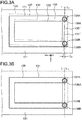
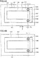
- the optical device 120 In order to assemble the optical device 120 having such a configuration and structure, it is necessary to precisely align the first holographic diffraction grating 131 and the second holographic diffraction grating 135 with each other. In particular, it is important to control and manage parallelism on an extending direction of first interference fringes formed in the first holographic diffraction grating 131 and an extending direction of second interference fringes formed in the second holographic diffraction grating 135.
- the following form can be provided: in a state where the relative alignment of the first holographic diffraction grating and the second holographic diffraction grating is completed, the first A alignment mark and the second A alignment mark are disposed at positions where the first A alignment mark and the second A alignment mark do not overlap, and the first B alignment mark and the second B alignment mark are disposed at positions where the first B alignment mark and the second B alignment mark do not overlap.
- the first A alignment mark and the second A alignment mark are imaged by a first imaging device; and the first B alignment mark and the second B alignment mark are imaged by a second imaging device.
- the imaging device may be an imaging device having a well-known configuration and structure.
- the first holographic diffraction grating is disposed on a first surface of the light guide plate; and the second holographic diffraction grating is disposed on a second surface of the light guide plate, the second surface being opposed to the first surface.
- the term "semi-transmissive" is used in some cases. This term is used in not a meaning that 1/2 (50%) of incident light is transmitted or reflected, but a meaning that part of incident light is transmitted and the rest is reflected.
- the spatial light modulation device examples include a light valve, for example, a transmissive-type or reflection-type liquid crystal display device such as an LCOS (Liquid Crystal On Silicon), and a digital micromirror device (DMD).
- a light valve for example, a transmissive-type or reflection-type liquid crystal display device such as an LCOS (Liquid Crystal On Silicon), and a digital micromirror device (DMD).
- the light source include the light emitting elements described above.
- the reflection-type spatial light modulation device can include a liquid crystal display device and a polarizing beam splitter. The polarizing beam splitter reflects part of light from the light source and guides the light to the liquid crystal display device, and causes part of the light reflected by the liquid crystal display device to pass to guide the light to an optical system.
- each casing 113 may be detachably attached to the temple portion of the frame of the eyeglasses owned by the observer with the mounting member 19.
- Each casing 113 may be attached to the outer side of the temple portion 13 or to the inner side of the temple portion 13.
- the first holographic diffraction grating 131 and the second holographic diffraction grating 135 are relatively aligned with each other.
- the shapes of the first A alignment mark, the second A alignment mark, the first B alignment mark, and the second B alignment mark are prescribed, or the arrangement of those alignment marks is prescribed. So, the first holographic diffraction grating and the second holographic diffraction grating can be relatively aligned with each other certainly and easily based on a simplified method.
- an image forming device including, as shown in Fig. 21 as a conceptual diagram, light emitting panels 511R, 511G, and 511B on which light emitting elements 501R, 501G, and 501B are arranged in a two-dimensional matrix, respectively.
- Light beams output from the light emitting panels 511R, 511G, and 511B are input to a dichroic prism 503 and collected into one optical path.
- the passages/non-passages of the light beams output from the dichroic prism 503 are controlled by a light passage control device 504, and the light beams are input to the light guide plate 121 via the collimating optical system 112.
Description
- The present disclosure relates to an optical device.
- In order for an observer to observe a two-dimensional image formed by an image forming device in an enlarged form by a virtual image optical system, a virtual image display device (image display device) using a holographic diffraction grating is well known. As shown in a conceptual diagram of
Fig. 1 , animage display device 100 basically includes animage forming device 111, a collimatingoptical system 112, and an optical device (light guide unit) 120. Theimage forming device 111 displays an image. Theoptical device 120 receives light displayed in theimage forming device 111 and guides the light to apupil 21 of an observer. Theoptical device 120 includes alight guide plate 121, a firstdiffraction grating member 130, and a seconddiffraction grating member 140. The firstdiffraction grating member 130 and the seconddiffraction grating member 140 are formed of holographic diffraction gratings provided to thelight guide plate 121. Light beams output from pixels of theimage forming device 111 are input to the collimatingoptical system 112, and a plurality of parallel light beams whose angles input to thelight guide plate 121 by the collimatingoptical system 112 are different from one another are generated and input to thelight guide plate 121. The plurality of parallel light beams are input from asecond surface 123 of thelight guide plate 121 and then output. A first holographic diffraction grating 131 that forms the firstdiffraction grating member 130 and the seconddiffraction grating member 140 are attached to afirst surface 122 of thelight guide plate 121. Meanwhile, a second holographic diffraction grating 135 that forms the firstdiffraction grating member 130 is attached to thesecond surface 123 of thelight guide plate 121. Thesecond surface 123 is parallel to thefirst surface 122 of thelight guide plate 121. The details of theimage display device 100 described above will be described in Embodiment 1. - In order to assemble the
optical device 120 having such a configuration and structure, it is necessary to precisely align the first holographic diffraction grating 131 and the second holographic diffraction grating 135 with each other. In particular, it is important to control and manage parallelism on an extending direction of first interference fringes formed in the first holographic diffraction grating 131 and an extending direction of second interference fringes formed in the second holographic diffraction grating 135. - An alignment mark that is formed of interference fringes or a diffraction grating and provided on one substrate together with a hologram or a diffraction grating is well known from Japanese Patent Application Laid-open No.
Hei 09-068705 Hei 09-068705 alignment mark 14 and anopposing alignment mark 16 are captured bycameras monitor screen 20. Thealignment mark 14 is formed of interference fringes or a diffraction grating and provided to ahologram 10. Theopposing alignment mark 16 is formed of an opaque pattern made of metal or the like and provided to atarget substrate 15 that is a substrate for a liquid crystal display device. Subsequently, relative positions of thehologram 10 and thetarget substrate 15 are adjusted such that the center of an image 14' of thealignment mark 14 and the center of an image 16' of theopposing alignment mark 16 matches each other. It may be possible to form theopposing alignment mark 16 from a transparent phase pattern, like thealignment mark 14. - Previously proposed arrangements are disclosed in
US 2006/228073 A1 ,US 2002/001107 A1 andUS 2010/002183 A1 . - In Japanese Patent Application Laid-open No.
Hei 09-068705 opposing alignment mark 16 and thealignment mark 14 are formed of the same transparent hologram, that is, in a case where two alignment marks are formed of a transparent hologram. - So, it is desirable to provide an optical device capable of certainly and precisely align two holographic diffraction gratings with each other in an optical device including those two holographic diffraction gratings, an assembling method for the optical device, a holographic diffraction grating that forms the optical device, a display device including the optical device, and an alignment device suitable to execute an assembling method for the optical device.
- Various respective aspects and features of the invention are defined in the appended claims. Combinations of features from the dependent claims may be combined with features of the independent claims as appropriate and not merely as explicitly set out in the claims.
- Embodiments of the present invention relate to to an optical device and a head mounted display. More specifically, embodiments relate to an optical device used as, for example, a head mounted display (HMD), and to a holographic diffraction grating, a display device.
- According to an embodiment of the present disclosure, there is provided a holographic diffraction grating including
an interference fringe forming area in which interference fringes are formed; and
two alignment marks that are provided outside the interference fringe forming area in an extending direction of the interference fringes and opposed to each other with the interference fringe forming area being sandwiched therebetween,
each of the alignment marks including an interference fringe that is identical to the interference fringes provided to the interference fringe forming area,
each of the alignment marks having an annular shape in plan view. - According to another embodiment of the present disclosure, there is provided an optical device including:
- (a) a light guide plate configured to output light after the light is input to the light guide plate and propagated inside the light guide plate by total reflection;
- (b) a first deflection unit configured to deflect the light input to the light guide plate, to totally reflect the light input to the light guide plate inside the light guide plate; and
- (c) a second deflection unit configured to deflect the light propagated inside the light guide plate by total reflection, to output, from the light guide plate, part of the light propagated inside the light guide plate by total reflection,
the first deflection unit including a first holographic diffraction grating and a second holographic diffraction grating,
the first holographic diffraction grating including a first interference fringe forming area in which first interference fringes are formed,
the second holographic diffraction grating including a second interference fringe forming area in which second interference fringes are formed,
the first holographic diffraction grating including a first A alignment mark and a first B alignment mark that are provided outside the first interference fringe forming area in an extending direction of the first interference fringes and opposed to each other with the first interference fringe forming area being sandwiched therebetween,
the second holographic diffraction grating including a second A alignment mark and a second B alignment mark that are provided outside the second interference fringe forming area in an extending direction of the second interference fringes and opposed to each other with the second interference fringe forming area being sandwiched therebetween,
each of the first A alignment mark and the first B alignment mark including interference fringes that are identical to the interference fringes provided to the first interference fringe forming area,
each of the second A alignment mark and the second B alignment mark including interference fringes that are identical to the interference fringes provided to the second interference fringe forming area,
in a state where a relative alignment of the first holographic diffraction grating and the second holographic diffraction grating is completed, each of the first A alignment mark and the second A alignment mark having a shape for which the first A alignment mark and the second A alignment mark do not overlap and each of the first B alignment mark and the second B alignment mark having a shape for which the first B alignment mark and the second B alignment mark do not overlap, or in the state where the relative alignment of the first holographic diffraction grating and the second holographic diffraction grating is completed, the first A alignment mark and the second A alignment mark being disposed at positions where the first A alignment mark and the second A alignment mark do not overlap and the first B alignment mark and the second B alignment mark being disposed at positions where the first B alignment mark and the second B alignment mark do not overlap. - According to another embodiment of the present disclosure, there is provided a display device including:
- (i) a frame mounted onto a head of an observer (for example, eyeglasses-type frame); and
- (ii) an image display device attached to the frame, the image display device including
- (A) an image forming device, and
- (B) an optical device configured to input light output from the image forming device and to output the light. The optical device includes the optical device according to the embodiment of the present disclosure described above.
- In some embodiments, an optical device is provided, comprising: a light guide comprising an input region and an output region, wherein the light guide is adapted to receive light at the input region and output at least some of the received light at the output region; and at least first and second diffraction gratings, wherein: the first diffraction grating is disposed on a first surface of the light guide, the first surface facing away from a light input, the second diffraction grating is disposed on a second surface of the light guide, the second surface facing towards the light input, the second diffraction grating is disposed at the input region of the light guide and adapted to diffract at least some of the light input into the light guide, and the first diffraction grating is adapted to diffract at least some light transmitted through the light guide back into the light guide.
- In some embodiments, a head mounted display is provided, comprising: a light guide comprising an input region and an output region, wherein the light guide is adapted to receive light at the input region and output at least some of the received light at the output region; at least first and second diffraction gratings, wherein: the first diffraction grating is disposed on a first surface of the light guide, the first surface facing away from a light input, the second diffraction grating is disposed on a second surface of the light guide, the second surface facing towards the light input, the second diffraction grating is disposed at the input region of the light guide and adapted to diffract and reflect at least some of the light input into the light guide to be propagated inside the light guide towards the output region, and the first diffraction grating is adapted to diffract and reflect at least some light transmitted through the light guide back into the light guide; alignment marks A1 and B1 associated with the first diffraction grating; and alignment marks A2 and B2 associated with the second diffraction grating.
- In some embodiments, a head mounted display is provided, comprising: a light guide; at least first and second diffraction gratings, wherein: the first diffraction grating is disposed on a first surface of the light guide, the first surface facing away from a light input, the second diffraction grating is disposed on a second surface of the light guide, the second surface facing towards the light input, the second diffraction grating is adapted to diffract and reflect at least some of the light input into the light guide to be propagated inside the light, and the first diffraction grating is adapted to diffract and reflect at least some light transmitted through the light guide back into the light guide; alignment marks A1 and B1 associated with the first diffraction grating; and alignment marks A2 and B2 associated with the second diffraction grating.
- These and other objects, features and advantages of the present disclosure will become more apparent in light of the following detailed description of best embodiment embodiments thereof, as illustrated in the accompanying drawings.
- Embodiments of the invention will now be described with reference to the accompanying drawings, throughout which like parts are referred to by like references, and in which:
-
Fig. 1 is a conceptual diagram of an image display device in a display device of Embodiment 1; -
Figs. 2A and 2B are a schematic diagram showing a light guide plate in the display device of Embodiment 1 when viewed from the opposite side of an observer, and a schematic diagram showing the light guide plate when viewed from the same side as the observer, respectively; -
Figs. 3A and 3B are schematic partial plan views of the light guide plate and the like, for describing an alignment of a first holographic diffraction grating and a second holographic diffraction grating; -
Figs. 4A and 4B are schematic partial plan views of the light guide plate and the like, for describing the alignment of the first holographic diffraction grating and the second holographic diffraction grating in a modification of the example shown inFigs. 3A and 3B ; -
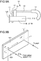
Figs. 5A and 5B are schematic partial cross-sectional views of the light guide plate and the like, for describing the alignment of the first holographic diffraction grating and the second holographic diffraction grating; -
Fig. 6 is a schematic cross-sectional view of a reflection-type volume holographic diffraction grating in a partially enlarged form in the display device of Embodiment 1; -
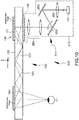
Fig. 7 is a schematic diagram of the display device of Embodiment 1 when viewed from above; -
Fig. 8 is a schematic diagram of the display device of Embodiment 1 when viewed from the front; -
Figs. 9A and 9B are a schematic diagram of the display device of Embodiment 1 when viewed from a lateral direction and a schematic diagram showing light propagation in the light guide plate that forms the image display device, respectively; -
Fig. 10 is a conceptual diagram of an image display device in a display device ofEmbodiment 2; -
Fig. 11 is a schematic diagram of the display device of Embodiment 3 when viewed from the front; -
Fig. 12 is a schematic diagram of the display device of Embodiment 3 (in a state assuming that a frame is removed) when viewed from the front; -
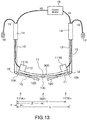
Fig. 13 is a schematic diagram of the display device of Embodiment 3 when viewed from above; -
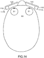
Fig. 14 is a diagram showing a state where the display device of Embodiment 3 is mounted onto the head of the observer when viewed from above (showing only the image display devices and omitting the illustration of the frame); -
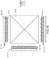
Fig. 15 is a schematic diagram of a display device of Embodiment 4 when viewed from the front; -
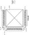
Fig. 16 is a schematic diagram of the display device of Embodiment 4 (in a state assuming that a frame is removed) when viewed from the front; -
Fig. 17 is a schematic diagram of the display device of Embodiment 4 when viewed from above; -
Fig. 18 is a conceptual diagram of a modification of an image forming device suitable for use in Embodiments 1 to 4; -
Fig. 19 is a conceptual diagram showing another modification of an image forming device suitable for use in Embodiments 1 to 4; -
Fig. 20 is a conceptual diagram showing another modification of an image forming device suitable for use in Embodiments 1 to 4; -
Fig. 21 is a conceptual diagram showing another modification of an image forming device suitable for use in Embodiments 1 to 4; and -
Fig. 22 is a conceptual diagram showing another modification of an image forming device suitable for use in Embodiments 1 to 4. - Hereinafter, the present disclosure will be described based on embodiments with reference to the drawings but is not limited to the embodiments. Various numerical values and materials in the embodiments are merely exemplary ones. It should be noted that the description is given in the following order.
- 1. General Description on Optical Device According to Embodiment of Present Disclosure, Assembling Method for Optical Device, Holographic Diffraction Grating According to Embodiment of Present Disclosure, Display Device According to Embodiment of Present Disclosure, and Alignment Device.
- 2. Embodiment 1 (Optical Device According to Embodiment of Present Disclosure, Assembling Method for Optical Device, Holographic Diffraction Grating According to Embodiment of Present Disclosure, Display Device According to Embodiment of Present Disclosure, and Alignment Device.)
- 3. Embodiment 2 (Modification of Embodiment 1)
- 4. Embodiment 3 (Modification of Embodiments 1 and 2)
- 5. Embodiment 4 (Modification of Embodiment 3) and Others
- In an assembling method for an optical device, the following form can be provided: with a first holographic diffraction grating being disposed on a light guide plate, the first holographic diffraction grating and a second holographic diffraction grating are relatively aligned with each other, and the second holographic diffraction grating is disposed on the light guide plate. In this case, it is desirable to move the light guide plate relative to the second holographic diffraction grating, with the first holographic diffraction grating being disposed on the light guide plate. Further, in those cases, after the first holographic diffraction grating is bonded to or formed on the light guide plate, the first holographic diffraction grating and the second holographic diffraction grating are relatively aligned with each other and the second holographic diffraction grating is bonded to the light guide plate. However, the present disclosure is not limited to the above configurations.
- In the assembling method for an optical device including the various desirable forms described above, the following form can be provided: with the second holographic diffraction grating being supported by a support, the first holographic diffraction grating and the second holographic diffraction grating are relatively aligned with each other. In this case, a first A alignment mark and a first B alignment mark are provided with interference fringes that are identical to interference fringes provided to a first interference fringe forming area, a second A alignment mark and a second B alignment mark are provided with interference fringes that are identical to interference fringes provided to a second interference fringe forming area, light is input to the light guide plate from an end surface of the light guide plate, the light diffracted and reflected on the first A alignment mark and the first B alignment mark is optically detected, the light is input to the support from an end surface of the light support, and the light diffracted and reflected on the second A alignment mark and the second B alignment mark is optically detected.
- Further, in the configuration described above in the assembling method for an optical device or in the assembling method for an optical device including the various desirable forms described above, the following form can be provided: in a state where the relative alignment of the first holographic diffraction grating and the second holographic diffraction grating is completed, each of the first A alignment mark and the second A alignment mark has a shape by which the first A alignment mark and the second A alignment mark do not overlap, and each of the first B alignment mark and the second B alignment mark has a shape for which the first B alignment mark and the second B alignment mark do not overlap. Alternatively, the following form can be provided: in a state where the relative alignment of the first holographic diffraction grating and the second holographic diffraction grating is completed, the first A alignment mark and the second A alignment mark are disposed at positions where the first A alignment mark and the second A alignment mark do not overlap, and the first B alignment mark and the second B alignment mark are disposed at positions where the first B alignment mark and the second B alignment mark do not overlap.
- It is desirable to adopt the following form: from a first light source in the assembling method for an optical device or in an alignment device, light beams input to the first A alignment mark and the first B alignment mark are diffracted and reflected on the first A alignment mark and the first B alignment mark, and such light that is output from the light guide plate at an output angle iout is output; and from a second light source, light beams input to the second A alignment mark and the second B alignment mark are diffracted and reflected on the second A alignment mark and the second B alignment mark, and such light that is output from the light guide plate at an output angle iout is output. Here, examples of the output angle iout include 0 degrees. Further, in order to obtain such a state, the wavelength of light output from the first light source and an incident angle on the light guide plate only need to be selected, or in order to obtain such a state, the wavelength of light output from the second light source and an incident angle on the support only need to be selected. Furthermore, it is desirable that parallel light be output from the first light source and parallel light be output from the second light source.
- Additionally, in the assembling method for an optical device including the various desirable forms and configurations described above, in an optical device according to an embodiment of the present disclosure, and in a display device according to an embodiment of the present disclosure, the following form can be provided: the first A alignment mark and the second A alignment mark are imaged by a first imaging device; and the first B alignment mark and the second B alignment mark are imaged by a second imaging device. The imaging device may be an imaging device having a well-known configuration and structure.
- Additionally, in the assembling method for an optical device including the various desirable forms and configurations described above, in an optical device according to an embodiment of the present disclosure, and in a display device according to an embodiment of the present disclosure, the following form can be provided: the first holographic diffraction grating is disposed on a first surface of the light guide plate; and the second holographic diffraction grating is disposed on a second surface of the light guide plate, the second surface being opposed to the first surface.
- Additionally, in the assembling method for an optical device including the various desirable forms and configurations described above, in an optical device according to an embodiment of the present disclosure, and in a display device according to an embodiment of the present disclosure, there can be provided a form satisfying the following expressions:
- P1≠P2 and ϕ1=ϕ2;
- P1=P2 and ϕ1≠ϕ2; or
- P1≠P2 and ϕ1≠ϕ2,
- Additionally, in the assembling method for an optical device including the various desirable forms and configurations described above, in an optical device according to an embodiment of the present disclosure, and in a display device according to an embodiment of the present disclosure, the following form can be provided: the first A alignment mark, the first B alignment mark, the second A alignment mark, and the second B alignment mark are each disposed on an end of the light guide plate.
- Additionally, in the assembling method for an optical device including the various desirable forms and configurations described above, it is desirable that the prescribed value have the maximum value of 100 seconds, but the present disclosure is not limited thereto.
- Additionally, in the assembling method for an optical device including the various desirable forms and configurations described above, in an optical device according to an embodiment of the present disclosure, and in a display device according to an embodiment of the present disclosure, the following form can be provided: the second deflection unit includes a holographic diffraction grating. In this case, it is desirable that the second deflection unit have a diffraction efficiency value that is smaller than a diffraction efficiency value of the first deflection unit. The diffraction efficiency value of the second deflection unit is made smaller than the diffraction efficiency value of the first deflection unit, and thus images observed by an observer along an axis direction of the light guide plate can be made uniform. In order that the diffraction efficiency value of the second deflection unit is made smaller than the diffraction efficiency value of the first deflection unit, for example, the thickness of the holographic diffraction grating that forms the second deflection unit only needs to be made smaller than the thickness of the holographic diffraction grating that forms the first deflection unit. It should be noted that hereinafter the holographic diffraction grating that forms the second deflection unit may be referred to as a "third holographic diffraction grating" for sake of simplicity.
- Further, in a holographic diffraction grating according to an embodiment of the present disclosure, the following form can be provided: each alignment mark is provided to the outside of a portion of an interference fringe forming area on the opposite side of a portion of the interference fringe forming area, from which light is output.
- In the optical device according to an embodiment of the present disclosure including the various desirable forms and configurations described above, in the assembling method for an optical device according to the first and second embodiments of the present disclosure, in the holographic diffraction grating according to an embodiment of the present disclosure, and in a display device according to an embodiment of the present disclosure, examples of the holographic diffraction grating include a reflection-type volume holographic diffraction grating. The reflection-type volume holographic diffraction grating means a holographic diffraction grating that diffracts and reflects only positive first-order diffracted light. In the first deflection unit, in order that the parallel light input to the light guide plate is totally reflected inside the light guide plate, at least part of the parallel light input to the light guide plate is diffracted and reflected. On the other hand, in the second deflection unit, the parallel light that is propagated inside the light guide plate by total reflection is diffracted and reflected a plurality of times and output from the light guide plate in the state of parallel light.
- An optical device assembled by the assembling method for an optical device can form a display device such as a head mounted display (HMD), and a display device according to an embodiment of the present disclosure can form a head mounted display (HMD), for example. This allows reduction in weight and downsizing of the display device and allows an uncomfortable feeling when the display device is mounted to be largely reduced. Further, this allows reduction in manufacture costs.
- In the display device according to an embodiment of the present disclosure, the optical device can be of a transmissive type or a semi-transmissive type (see-through type). Specifically, at least a part of the optical device, which is opposed to the pupil of the observer, can be made transmissive or semi-transmissive (see-through), and thus a landscape can be viewed through the part of the optical device. The display device may include one image display device (monocular type) or two image display devices (binocular type).
- In this specification, the term "semi-transmissive" is used in some cases. This term is used in not a meaning that 1/2 (50%) of incident light is transmitted or reflected, but a meaning that part of incident light is transmitted and the rest is reflected.
- The optical device according to an embodiment of the present disclosure or the display device according to an embodiment of the present disclosure allows monochrome (for example, green) image display. In this case, the angle of view is divided into two, for example (more specifically, into two halves, for example), and the first deflection unit can be formed of a laminate of two holographic diffraction gratings corresponding to respective groups of the angle of view divided into two. Alternatively, in the case of color image display, in order to correspond to diffraction reflection of P types of light beams having different P types (for example, P=3, i.e., three types of red, green, and blue) of wavelength bands (or wavelengths), each of the first deflection unit and the second deflection unit can be a laminate of P layers of holographic diffraction gratings. In this case, for each holographic diffraction grating, interference fringes corresponding to one type of wavelength band (or wavelength) are formed. Alternatively, for example, the following structure may be adopted: a holographic diffraction grating that causes light having a red wavelength band (or wavelength) to be diffracted and reflected is disposed on the first light guide plate; a holographic diffraction grating that causes light having a green wavelength band (or wavelength) to be diffracted and reflected is disposed on the second light guide plate; a holographic diffraction grating that causes light having a blue wavelength band (or wavelength) to be diffracted and reflected is disposed on the third light guide plate; and those first light guide plate, second light guide plate, and third light guide plate are laminated with gaps therebetween. Adopting this configuration allows an increase in diffraction efficiency when light beams having respective wavelength bands (or wavelengths) are diffracted and reflected in holographic diffraction gratings, an increase in diffraction reception angle, and optimization of diffraction-reflection angle. The lamination of the holographic diffraction gratings may be performed using the alignment device based on the assembling method for an optical device according to the first and second embodiments of the present disclosure, and the holographic diffraction grating may be formed of the holographic diffraction grating according to an embodiment of the present disclosure. It is desirable to dispose a protector such that the holographic diffraction grating does not come into direct contact with air.
- Examples of material forming the holographic diffraction grating include a photopolymer material. A constituent material and a basic structure of the holographic diffraction grating may be the same as those of a holographic diffraction grating in related art. Although interference fringes are formed inside and over the surface of the holographic diffraction grating, a method of forming the interference fringes may be the same as a forming method in related art. Specifically, for example, object light may be applied to a member that forms a holographic diffraction grating (for example, photopolymer material) from a first predetermined direction on one side, and reference light may be applied to the member that forms a holographic diffraction grating from a second predetermined direction on the other side at the same time, to record interference fringes formed by the object light and the reference light in the member that forms a holographic diffraction grating. When the first predetermined direction, the second predetermined direction, and the wavelengths of the object light and the reference light are adequately selected, a desired pitch of interference fringes on the surface of the holographic diffraction grating and a desired slant angle (angle of inclination) of the interference fringes can be obtained. The slant angle of the interference fringes means an angle formed by the surface of the holographic diffraction grating and the interference fringes.
- The optical device can be manufactured by the following method, for example.
- (A-1) Form a first holographic diffraction grating and a third holographic diffraction grating on a first surface of a substrate for manufacture (that doubles as a support in some cases).
- (A-2) Form a second holographic diffraction grating on a second surface of the substrate for manufacture.
- (A-3) Transfer the first holographic diffraction grating and the third holographic diffraction grating, which are formed on the first surface of the substrate for manufacture, to a first surface of a light guide plate, and transfer the second holographic diffraction grating, which is formed on the second surface of the substrate for manufacture, to a second surface of the light guide plate.
- Alternatively, the optical device can be manufactured by the following method.
- (B-1) Form a first holographic diffraction grating and a third holographic diffraction grating on a first surface of a light guide plate.
- (B-2) Form a second holographic diffraction grating on a substrate for manufacture (that doubles as a support in some cases).
- (B-3) Transfer the second holographic diffraction grating, which is formed on the substrate for manufacture, to a second surface of the light guide plate.
- Alternatively, the optical device can be manufactured by the following method.
- (C-1) Form a second holographic diffraction grating on a second surface of a light guide plate.
- (C-2) Form a first holographic diffraction grating and a third holographic diffraction grating on a substrate for manufacture (that doubles as a support in some cases).
- (C-3) Transfer the first holographic diffraction grating and the third holographic diffraction grating, which are formed on the substrate for manufacture, to a first surface of the light guide plate.
- Alternatively, the optical device can be manufactured by the following method.
- (D-1) Form a first holographic diffraction grating and a third holographic diffraction grating on a first substrate for manufacture.
- (D-2) Form a second holographic diffraction grating on a second substrate for manufacture (that doubles as a support in some cases).
- (D-3) Transfer the first holographic diffraction grating and the third holographic diffraction grating, which are formed on the first substrate for manufacture, to a first surface of a light guide plate, and transfer the second holographic diffraction grating, which is formed on the second substrate for manufacture, to a second surface of the light guide plate.
- Alternatively, the optical device can be manufactured by the following method.
- (E-1) Form a first holographic diffraction grating on a first substrate for manufacture.
- (E-2) Form a second holographic diffraction grating on a second substrate for manufacture (that doubles as a support in some cases).
- (E-3) Form a third holographic diffraction grating on a third substrate for manufacture.
- (E-4) Transfer the first holographic diffraction grating formed on the first substrate for manufacture and the third holographic diffraction grating formed on the third substrate for manufacture to a first surface of a light guide plate, and transfer the second holographic diffraction grating formed on the second substrate for manufacture to a second surface of the light guide plate.
- In the image display device, the image forming device can have a form including a plurality of pixels arranged in a two-dimensional matrix. It should be noted that the image forming device having such a configuration is referred to as an "image forming device having a first configuration" for sake of simplicity.
- Examples of the image forming device having a first configuration include: an image forming device including a reflection-type spatial light modulation device and a light source; an image forming device including a transmissive-type spatial light modulation device and a light source; and an image forming device including a light emitting element such as a light-emitting diode (LED), a semiconductor laser element, an organic EL (Electro Luminescence) element, or an inorganic EL element. Of those, it is desirable to use an image forming device including a reflection-type spatial light modulation device and a light source. Examples of the spatial light modulation device include a light valve, for example, a transmissive-type or reflection-type liquid crystal display device such as an LCOS (Liquid Crystal On Silicon), and a digital micromirror device (DMD). Examples of the light source include the light emitting elements described above. Further, the reflection-type spatial light modulation device can include a liquid crystal display device and a polarizing beam splitter. The polarizing beam splitter reflects part of light from the light source and guides the light to the liquid crystal display device, and causes part of the light reflected by the liquid crystal display device to pass to guide the light to an optical system. Examples of the light emitting element that forms the light source include a red light emitting element, a green light emitting element, a blue light emitting element, and a white light emitting element. Alternatively, red light, green light, and blue light that are output from the red light emitting element, the green light emitting element, and the blue light emitting element, respectively, may be used to achieve color mixture and uniformity in luminance by using a light pipe, to obtain white light. Examples of the light emitting element include a semiconductor laser element, a solid-state laser, and an LED. The number of pixels may be determined based on the specifications requested for the image display device and take specific values such as 320*240, 432*240, 640*480, 854*480, 1024*768, and 1920*1080, for example. A collimating optical system that will be described later has a function of converting position information of a pixel into angle information in an optical system of a light guide unit. Examples of the collimating optical system include an optical system that includes a convex lens, a concave lens, a free-form-surface prism, and a hologram lens independently or in combination and has a positive optical power as a whole.
- Alternatively, in the image display device, the image forming device can have a form including a light source and a scanning unit that scans parallel light output from the light source. It should be noted that the image forming device having such a configuration is referred to as an "image forming device having a second configuration" for sake of simplicity.
- Examples of the light source in the image forming device having a second configuration include a light emitting element, specifically, a red light emitting element, a green light emitting element, a blue light emitting element, and a white light emitting element. Alternatively, red light, green light, and blue light that are output from the red light emitting element, the green light emitting element, and the blue light emitting element, respectively, may be used to achieve color mixture and uniformity in luminance by using a light pipe, to obtain white light. Examples of the light emitting element include a semiconductor laser element, a solid-state laser, and an LED. The number of pixels (virtual pixels) in the image forming device having a second configuration may also be determined based on the specifications requested for the image display device and take specific values such as 320*240, 432*240, 640*480, 854*480, 1024*768, and 1920*1080, for example. Further, in the case of color image display and in the case where the light source includes a red light emitting element, a green light emitting element, and a blue light emitting element, for example, it is desirable to perform color composition by using a cross prism. Examples of the scanning unit include MEMS (Micro Electro Mechanical Systems) including a micromirror that is rotatable in two-dimensional directions and horizontally and vertically scans light output from the light source, and a galvanometer mirror. A relay optical system that will be described later may be formed of a well-known relay optical system.
- In the image forming device having a first configuration or the image forming device having a second configuration, the light that is changed into a plurality of parallel light beams in the optical system is input to the light guide plate. Such an optical system is an optical system in which output light is assumed as parallel light and which is referred to as a "parallel light outputting optical system" in some cases, and specifically, includes a collimating optical system or a relay optical system, for example. In such a manner, being parallel light is requested based on the necessity to preserve light wavefront information obtained when those light beams are input to the light guide plate, even after those light beams are output from the light guide plate via the first deflection unit and the second deflection unit. In order to generate a plurality of parallel light beams, specifically, for example, a light output unit of the image forming device may be provided at a spot (position) of the focal distance in the parallel light outputting optical system, for example. The parallel light outputting optical system has a function of converting position information of a pixel into angle information in the optical system of the optical device. Examples of the parallel light outputting optical system include an optical system that includes a convex lens, a concave lens, a free-form-surface prism, and a hologram lens independently or in combination and has a positive optical power as a whole. A light blocking unit having an opening may be disposed between the parallel light outputting optical system and the light guide plate so as to prevent undesired light from being output from the parallel light outputting optical system and input to the light guide plate.
- Alternatively, for example, in addition to a combination of a backlight that emits white light as a whole and a liquid crystal display device including red light emitting pixels, green light emitting pixels, and blue light emitting pixels, examples of the light source or the image forming device including light emitting elements and light valves include the following configurations.
- An image forming device A includes
- (α) a first image forming device including a first light emitting panel on which first light emitting elements that emit blue light are arranged in a two-dimensional matrix,
- (β) a second image forming device including a second light emitting panel on which second light emitting elements that emit green light are arranged in a two-dimensional matrix,
- (γ) a third image forming device including a third light emitting panel on which third light emitting elements that emit red light are arranged in a two-dimensional matrix, and
- (δ) a unit for collecting light beams output from the first image forming device, the second image forming device, and the third image forming device into one optical path (for example, the unit corresponds to a dichroic prism; the same holds true for the following description), in which
the light-emitting/non-light-emitting states of the first light emitting elements, the second light emitting elements, and the third light emitting elements are controlled. - An image forming device B includes
- (α) a first image forming device including a first light emitting element that emits blue light, and a first light passage control device for controlling the passage/non-passage of output light output from the first light emitting element that emits blue light, the first light passage control device being a kind of light valve and including a liquid crystal display device, a digital micromirror device (DMD), and a LCOS, for example; the same holds true for the following description,
- (β) a second image forming device including a second light emitting element that emits green light, and a second light passage control device (light valve) for controlling the passage/non-passage of output light output from the second light emitting element that emits green light,
- (γ) a third image forming device including a third light emitting element that emits red light, and a third light passage control device (light valve) for controlling the passage/non-passage of output light output from the third light emitting element that emits red light, and
- (δ) a unit for collecting light beams passing through the first light passage control device, the second light passage control device, and the third light passage control device into one optical path,
in which the passage/non-passage of the output light beams output from those light emitting elements is controlled by the light passage control devices, and thus an image is displayed. Examples of units for leading the output light beams output from the first light emitting element, the second light emitting element, and the third light emitting element (i.e., light leading members) include light guide members, microlens arrays, mirrors or reflective plates, and condenser lenses. - An image forming device C includes
- (α) a first image forming device including a first light emitting panel on which first light emitting elements that emit blue light are arranged in a two-dimensional matrix, and a blue light passage control device (light valve) for controlling the passage/non-passage of output light output from the first light emitting panel,
- (β) a second image forming device including a second light emitting panel on which second light emitting elements that emit green light are arranged in a two-dimensional matrix, and a green light passage control device (light valve) for controlling the passage/non-passage of output light output from the second light emitting panel,
- (γ) a third image forming device including a third light emitting panel on which third light emitting elements that emit red light are arranged in a two-dimensional matrix, and a red light passage control device (light valve) for controlling the passage/non-passage of output light output from the third light emitting panel, and
- (δ) a unit for collecting light beams passing through the blue light passage control device, the green light passage control device, and the red light passage control device into one optical path,
in which the passage/non-passage of the output light beams output from those first light emitting panel, second light emitting panel, and third light emitting panel is controlled by the light passage control devices (light valves), and thus an image is displayed. - An image forming device D, which is an image forming device for color display of a field sequential system, includes
- (α) a first image forming device including a first light emitting element that emits blue light,
- (β) a second image forming device including a second light emitting element that emits green light,
- (γ) a third image forming device including a third light emitting element that emits red light,
- (δ) a unit for collecting light beams output from the first image forming device, the second image forming device, and the third image forming device into one optical path, and
- (ε) a light passage control device (light valve) for controlling the passage/non-passage of the light output from the unit for collecting light beams into one optical path,
in which the passage/non-passage of the output light beams output from those light emitting elements is controlled by the light passage control devices, and thus an image is displayed. - An image forming device E, which is also an image forming device for color display of a field sequential system, includes
- (α) a first image forming device including a first light emitting panel on which first light emitting elements that emit blue light are arranged in a two-dimensional matrix,
- (β) a second image forming device including a second light emitting panel on which second light emitting elements that emit green light are arranged in a two-dimensional matrix,
- (γ) a third image forming device including a third light emitting panel on which third light emitting elements that emit red light are arranged in a two-dimensional matrix,
- (δ) a unit for collecting light beams output from the respective first image forming device, second image forming device, and third image forming device into one optical path, and
- (ε) a light passage control device (light valve) for controlling the passage/non-passage of the light output from the unit for collecting light beams into one optical path,
in which the passage/non-passage of the output light beams output from those light emitting panels is controlled by the light passage control device, and thus an image is displayed. - An image forming device F is an image forming device for color display of a passive matrix type or an active matrix type in which an image is displayed by controlling the light-emitting/non-light-emitting states of first light emitting elements, second light emitting elements, and third light emitting elements.
- An image forming device G, which is an image forming device for color display of a field sequential system, includes
light passage control devices (light valves) for controlling the passage/non-passage of output light beams from light emitting element units arranged in a two-dimensional matrix,
in which the light-emitting/non-light-emitting states of first light emitting elements, second light emitting elements, and third light emitting elements in the light emitting element units are controlled on a time division basis, and further the passage/non-passage of the output light beams output from the first light emitting elements, second light emitting elements, and third light emitting elements is controlled by the light passage control devices, and thus an image is displayed. - The light guide plate has two parallel surfaces (first surface and second surface) extending parallel to the axis of the light guide plate (the axis corresponds to a longitudinal direction or horizontal direction and is referred to as an "x axis" for sake of simplicity). It should be noted that the width direction of the light guide plate, which corresponds to a height direction or a vertical direction, is referred to as a "y axis" for sake of simplicity. Assuming that a surface of the light guide plate, to which light is input, is an input surface of the light guide plate, and a surface of the light guide plate, from which light is output, is an output surface of the light guide plate, the input surface of the light guide plate and the output surface of the light guide plate may be formed of the second surface. Alternatively, the input surface of the light guide plate may be formed of the first surface, and the output surface of the light guide plate may be formed of the second surface. The interference fringes of the holographic diffraction grating extend substantially parallel to the y axis.
- The first A alignment mark and the first B alignment mark are provided to the outside of the first interference fringe forming area in an extending direction of the first interference fringes so as to be opposed to each other while sandwiching the first interference fringe forming area therebetween. Specifically, however, the first A alignment mark and the first B alignment mark may be included in a projected image onto an x-z plane of the first interference fringe forming area or may be included in a projected image onto an x-z plane of a part of the first holographic diffraction grating on the end of the light guide plate in relation to the first interference fringe forming area (for sake of simplicity, the part is referred to as an "end area of the first holographic diffraction grating" in some cases). Similarly, the second A alignment mark and the second B alignment mark are provided to the outside of the second interference fringe forming area in an extending direction of the second interference fringes so as to be opposed to each other while sandwiching the second interference fringe forming area. Specifically, however, the second A alignment mark and the second B alignment mark may be included in a projected image onto an x-z plane of the second interference fringe forming area or may be included in a projected image onto an x-z plane of a part of the second holographic diffraction grating on the end of the light guide plate in relation to the second interference fringe forming area (for sake of simplicity, the part is referred to as an "end area of the second holographic diffraction grating" in some cases).
- Examples of the material forming the light guide plate include glasses including an optical glass such as a quartz glass or BK7, and plastic materials (for example, PMMA (poly methyl methacrylate), polycarbonate resin, acrylic resin, amorphous polypropylene resin, and styrene resin including AS resin (acrylonitrile styrene copolymer)). The shape of the light guide plate is not limited to be a flat shape and may be a curved shape. Examples of the material forming the support include a material forming the light guide plate, other plastic films, and dicing tapes (dicing films).
- In the display device according to an embodiment of the present disclosure, a frame includes a front portion disposed on the front of the observer, and two temple portions turnably attached to both ends of the front portion via hinges. It should be noted that earpiece portions are attached to the tip ends of the respective temple portions. The image display device is attached to the frame. Specifically, for example, the image forming device only needs to be attached to the temple portion. Further, a configuration in which the front portion and the two temple portions are incorporated can be adopted. In other words, when the whole of the display device according to an embodiment of the present disclosure is viewed, generally, the frame has substantially the same structure as that of normal eyeglasses. The materials forming the frame including a pad portion can be the same as materials forming normal eyeglasses, such as metals, alloys, plastics, and combinations thereof. Furthermore, a configuration in which nose pads are attached to the front portion can be adopted. In other words, when the whole of the display device according to an embodiment of the present disclosure is viewed, an assembled body of the frame and the nose pads has substantially the same structure as that of normal eyeglasses, except for the absence of a rim. The nose pads can have a well-known configuration and structure.
- Besides, in the display device according to an embodiment of the present disclosure, it is desirable to adopt a form in which wires (signal line, power supply line, etc.) extending from one or two image forming devices are extended from the tip ends of the earpiece portions to the outside through the inside of the temple portions and the earpiece portions and are connected to a control device (control circuit or control unit), from the viewpoint of design or ease of mounting. Further, each image forming device includes a headphone portion and can have a form in which headphone portion wires, which extend from the respective image forming devices, are extended from the tip ends of the earpiece portions to the headphone portions through the inside of the temple portions and the earpiece portions. Examples of the headphone portion include an inner ear type headphone portion and a canal type headphone portion. More specifically, it is desirable to adopt a form in which the headphone portion wire is extended to the headphone portion so as to run around the rear side of a pinna (auricle) from the tip end of the earpiece portion.
- It is possible to adopt a form in which an imaging device is attached to the center part of the front portion. Specifically, the imaging device includes a solid-state imaging device, which has a CCD (Charge Coupled Device) or a CMOS (Complementary Metal Oxide Semiconductor) sensor, and a lens, for example. The wiring from the imaging device only needs to be connected to one image display device (or image forming device) via the front portion for example, and only needs to be further included in wiring extending from the image display device (or image forming device).
- A light beam that is output from the center of the image forming device and passes through a nodal point on the image forming device side of the optical system is referred to as a "central light beam", and a light beam in the central light beam, which is vertically input to the optical device, is referred to as a "central incident light beam". It is assumed that a point at which the central incident light beam is input to the optical device is an optical device central point, an axis that passes through the optical device central point and is parallel to the axis direction of the optical device is an x axis, and an axis that passes through the optical device central point and coincides with the normal line of the optical device is an z axis. The horizontal direction in the display device according to an embodiment of the present disclosure is a direction that is parallel to the x axis, and is hereinafter referred to as an "x-axis direction" in some cases. Here, the optical system is disposed between the image forming device and the optical device and changes light output from the image forming device into parallel light. Subsequently, a light flux changed into the parallel light in the optical system is input to the optical device, guided to the optical device, and output from the optical device. Further, the central point of the first deflection unit is referred to as an "optical device central point".
- Alternatively, in the case where the display device is of a binocular type, the display device can have the following configuration: the light guide plate is disposed on the center of the observer's face in relation to the image forming device as a whole; a connection member to connect two image display devices is further provided; the connection member is attached to one side of the frame, which faces the observer at the central part located between two pupils of the observer; and a projected image of the connection member is included in a projected image of the frame.
- In such a manner, with the structure in which the connection member is attached to the central part of the frame that is located between the two pupils of the observer, i.e., without the structure in which the image display devices are directly attached to the frame, when the frame is mounted onto the head of the observer, the temple portions are expanded outwards. As a result, if the frame is deformed, such a deformation of the frame does not cause a displacement (positional change) of the image forming device or the light guide plate, or causes little displacement, if any. For that reason, the angle of convergence of left and right images can be certainly prevented from being changed. Moreover, since it is unnecessary to enhance the rigidity of the front portion of the frame, it is possible to avoid causing an increase in weight of the frame, lowering in design quality, and a rise in cost. Besides, since the image display devices are not attached directly to the eyeglasses-type frame, the design, color, and the like of the frame can be freely selected according to the observer's preference, and thus there are few restrictions imposed on the design of the frame and the degree of freedom on a design basis is high. In addition, the connecting member is disposed between the observer and the frame, and, moreover, the projected image of the connecting member is included in the projected image of the frame. In other words, when the head mounted display is viewed from the front of the observer, the connecting member is hidden behind the frame. So, a high design quality can be given to the head mounted display.
- It is desirable that the connection member be attached to the side, facing the observer, of the central part of the front portion located between the two pupils of the observer. The part corresponds to a bridge portion in normal eyeglasses.
- The two image display devices are connected to each other with the connection member. Specifically, the following form is provided: the image forming devices are attached to both ends of the connection member such that the mounting state can be adjusted. In this case, it is desirable that each of the image forming devices be located on the outside in relation to the pupil of the observer. In such a configuration, furthermore, it is desirable to satisfy:
- 0.01∗L≤α≤0.30∗L, desirably 0.05∗L≤α≤0.25∗L;
- 0.35∗L≤β≤0.65∗L, desirably 0.45∗L≤β≤0.55∗L; and
- 0.70∗L≤γ≤0.99∗L, desirably 0.75∗L≤γ≤0.95∗L,
- Here, the center of the mounting portion of the image forming device indicates a bisection point, along the axial direction of the frame, of a portion where a projected image of the image forming device, which is obtained by projecting the image forming device and the frame onto a virtual plane, is superimposed on a projected image of the frame, in the state where the image forming device is attached to the connection member. Further, the center of the connection member indicates a bisection point, along the axis direction of the frame, of a portion where the connection member is in contact with the frame, in the state where the connection member is attached to the frame. The length of the frame indicates the length of the projected image of the frame, in the case where the frame is curved. It should be noted that a projection direction is a direction vertical to the observer's face.
- Alternatively, the two image display devices are connected to each other with the connection member, and specifically, the following form can be adopted: two light guide plates are connected to each other with the connection member. There is a case where the two light guide plates are integrally manufactured, and in such a case, the connection member is attached to such a light guide plate integrally manufactured. Such a form is also included in the form in which the connection member connects the two light guide plates to each other. Assuming that a distance from the center of one of the image forming devices to one end of the frame is α' and a distance from the center of the other one of the image forming devices to the one end of the frame is γ', the values of α' and γ' are desirably set to the same as the values of α and γ described above. It should be noted that the center of the image forming device indicates a bisection point, along the axis direction of the frame, of a portion where a projected image of the image forming device, which is obtained by projecting the image forming device and the frame onto a virtual plane, is superimposed on a projected image of the frame, in the state where the image forming device is attached to the light guide plate.
- The shape of the connection member is substantially optional as long as the projected image of the connection member is included in the projected image of the frame. Examples of the shape of the connection member include bar-like shapes and strip-like shapes. Examples of the material forming the connecting member include metals, alloys, plastics, and combinations thereof.
- Embodiment 1 relates to an optical device according to an embodiment of the present disclosure, an assembling method for an optical device, a holographic diffraction grating according to an embodiment of the present disclosure, a display device (specifically, head mounted display (HMD)) according to an embodiment of the present disclosure, and an alignment device.
Fig. 1 is a conceptual diagram of an image display device in a display device according to an embodiment of Embodiment 1.Figs. 2A and 2B are a schematic diagram showing a light guide plate in the display device of Embodiment 1 when viewed from the opposite side of an observer, and a schematic diagram showing the light guide plate when viewed from the same side as the observer, respectively. It should be noted that inFigs. 2A and 2B , to clearly specify a first interference fringe forming area and a second interference fringe forming area, the first interference fringe forming area and the second interference fringe forming area are hatched. Further,Fig. 6 is a schematic cross-sectional view of a reflection-type volume holographic diffraction grating in a partially enlarged form in the display device of Embodiment 1.Fig. 7 is a schematic diagram of the display device of Embodiment 1 when viewed from above.Fig. 8 is a schematic diagram of the display device of Embodiment 1 when viewed from the front.Fig. 9A is a schematic diagram of the display device of Embodiment 1 when viewed from a lateral direction.Fig. 9B is a schematic diagram showing light propagation in the light guide plate that forms the image display device. - More specifically, the display device according to Embodiment 1 or
Embodiment 2 that will be described later is a head mounted display (HMD) including - (i) a frame (for example, eyeglasses-type frame 10) mounted onto the head of an
observer 20, and - (ii)
image display devices frame 10. Further, each of theimage display devices Embodiment 2 that will be described later includes- (A)
image forming devices - (B) optical devices (light guide units) to and from which light output from the
image forming devices - (C) optical systems (parallel light outputting optical systems) 112 and 254 that change light output from the
image forming devices optical systems optical device 120 and output. The optical device includes theoptical device 120 according to Embodiment 1. Specifically, the display device according to Embodiment 1 orEmbodiment 2 that will be described later is of a binocular type including two image display devices, but may be of a monocular type including one image display device. Theimage forming devices
- (A)
- The
image display devices frame 10 in a fixed manner or detachably. Theoptical systems image forming devices optical device 120. The light fluxes changed into the parallel light in theoptical systems optical device 120 and output. Further, theoptical device 120 is a semi-transmissive type (see-through type). Specifically, portions of the optical devices, which are opposed to at least the both eyes of the observer 20 (more specifically,light guide plate 121 andsecond deflection unit 140 that will be described later), are semi-transmissive (see-through). - In Embodiment 1 or
Embodiment 2 that will be described later, in a light beam (central incident light beam CL) that is output from the center of each of theimage forming devices optical systems optical device 120 is input to theoptical device 120 is an optical device central point O, an axis that passes through the optical device central point O and is parallel to the axis direction of theoptical device 120 is a y axis, and an axis that passes through the optical device central point O and coincides with the normal line of theoptical device 120 is a z axis. It should be noted that the central point of thefirst deflection unit 130 is the optical device central point O. In other words, as shown inFig. 9B , in theimage display devices image forming devices optical systems light guide plate 121. In other words, the central incident light beam CL is input to thelight guide plate 121 at an incident angle of 0 degrees. In this case, the center of the displayed image coincides with a direction of a perpendicular of thesecond surface 123 of thelight guide plate 121. - In the optical device according to an embodiment of the present disclosure, the optical device in the display device according to an embodiment of the present disclosure, and the assembling method for an optical device according to the first and second embodiments of the present disclosure, the
optical device 120 according to Embodiment 1 orEmbodiment 2 that will be described later includes - (a) a
light guide plate 121 configured to output light after the light is input to the light guide plate and propagated inside the light guide plate by total reflection, - (b) a
first deflection unit 130 configured to deflect the light input to thelight guide plate 121, to totally reflect the light input to thelight guide plate 121 inside thelight guide plate 121, and - (c) a
second deflection unit 140 configured to deflect the light propagated inside thelight guide plate 121 by total reflection, to output, from thelight guide plate 121, part of the light propagated inside thelight guide plate 121 by total reflection. Here, each of thefirst deflection unit 130 and thesecond deflection unit 140 is formed of a reflection-type volume holographic diffraction grating. In other words, thefirst deflection unit 130 and thesecond deflection unit 140 function as a kind of a semi-transmissive mirror. - Furthermore, the
first deflection unit 130 is formed of a firstholographic diffraction grating 131 and a secondholographic diffraction grating 135. The firstholographic diffraction grating 131 includes a first interferencefringe forming area 132 in which first interference fringes are formed. The secondholographic diffraction grating 135 includes a second interferencefringe forming area 136 in which second interference fringes are formed. - Further, the first
holographic diffraction grating 131 is provided with a firstA alignment mark 134A and a firstB alignment mark 134B, which are provided on anouter side 133 of the first interferencefringe forming area 132 in an extending direction of the first interference fringes so as to be opposed to each other while sandwiching the first interferencefringe forming area 132 therebetween. On the other hand, the secondholographic diffraction grating 135 is provided with a secondA alignment mark 138A and a secondB alignment mark 138B, which are provided on anouter side 137 of the second interferencefringe forming area 136 in an extending direction of the second interference fringes so as to be opposed to each other while sandwiching the second interferencefringe forming area 136 therebetween. Further, the firstA alignment mark 134A and the firstB alignment mark 134B are each provided with interference fringes that are identical to that of the first interferencefringe forming area 132, and the secondA alignment mark 138A and the secondB alignment mark 138B are each provided with interference fringes that are identical to that of the second interferencefringe forming area 136. - Further, in the optical device according to an embodiment of the present disclosure and in the display device according to an embodiment of the present disclosure, in a state where the relative alignment of the first
holographic diffraction grating 131 and the secondholographic diffraction grating 135 is completed, each of the firstA alignment mark 134A and the secondA alignment mark 138A has a shape for which the firstA alignment mark 134A and the secondA alignment mark 138A do not overlap, and each of the firstB alignment mark 134B and the secondB alignment mark 138B has a shape for which the firstB alignment mark 134B and the secondB alignment mark 138B do not overlap. Alternatively, simultaneously, in a state where the relative alignment of the firstholographic diffraction grating 131 and the secondholographic diffraction grating 135 is completed, the firstA alignment mark 134A and the secondA alignment mark 138A are disposed at positions where the firstA alignment mark 134A and the secondA alignment mark 138A do not overlap, and the firstB alignment mark 134B and the secondB alignment mark 138B are disposed at positions where the firstB alignment mark 134B and the secondB alignment mark 138B do not overlap. - In Embodiment 1 or
Embodiment 2 that will be described later, thefirst deflection unit 130 is disposed on each of thefirst surface 122 and thesecond surface 123 of thelight guide plate 121, and thesecond deflection unit 140 formed of the third holographic diffraction grating is disposed on thefirst surface 122 of thelight guide plate 121. In other words, the firstholographic diffraction grating 131 is disposed on thefirst surface 122 of thelight guide plate 121, and the secondholographic diffraction grating 135 is disposed on thesecond surface 123 that is opposed to thefirst surface 122 of thelight guide plate 121. Thefirst deflection unit 130 diffracts and reflects at least part of the light input to thelight guide plate 121 such that the parallel light input to thelight guide plate 121 is totally reflected inside thelight guide plate 121. Thesecond deflection unit 140 diffracts and reflects the light propagated inside thelight guide plate 121 by total reflection a plurality of times and outputs the light in the state of parallel light from thesecond surface 123 of thelight guide plate 121. In thefirst deflection unit 130, in order that the parallel light input to thelight guide plate 121 is totally reflected inside thelight guide plate 121, the parallel light input to thelight guide plate 121 is diffracted and reflected. On the other hand, in thesecond deflection unit 140, the parallel light that is propagated inside thelight guide plate 121 by total reflection is diffracted and reflected a plurality of times and output toward thepupil 21 of theobserver 20 from thelight guide plate 121 in the state of parallel light. The diffraction efficiency value of thesecond deflection unit 140 is smaller than the diffraction efficiency value of thefirst deflection unit 130. Specifically, the thickness of the third holographic diffraction grating that forms thesecond deflection unit 140 is smaller than the thickness of the firstholographic diffraction grating 131 and the secondholographic diffraction grating 135, each of which forms thefirst deflection unit 130. - In Embodiment 1 or
Embodiment 2 that will be described later, assuming that a pitch of the first interference fringes formed in the firstholographic diffraction grating 131 is P1, a slant angle is ϕ1, a pitch of the second interference fringes formed in the secondholographic diffraction grating 135 is P2, and a slant angle is ϕ2, for example, the following relationships are established: P1=P2 and ϕ1≠ϕ2. For that reason, light having the same wavelength is diffracted and reflected in the first interference fringes and the second interference fringes, but the incident angle at which the diffraction efficiency becomes the maximum differs, that is, an incident angle on the firstholographic diffraction grating 131 and an incident angle on the secondholographic diffraction grating 135 are different. Thus, the diffraction-reflection angle at which a light intensity of the diffracted and reflected light reaches a peak differs from each other. Further, the firstA alignment mark 134A, the firstB alignment mark 134B, the secondA alignment mark 138A, and the secondB alignment mark 138B are disposed on the end of thelight guide plate 121. - As in the display device according to Embodiment 1, in the case of monochrome (for example, green) image display, it is desirable that the angle of view be divided into two, for example (into two halves, for example) and the
first deflection unit 130 be formed of a laminate of the twoholographic diffraction gratings light guide plate 121, the angle of view of the parallel light that is input at an angle of a direction approaching thesecond deflection unit 140 is a negative angle of view and the angle of view of the parallel light that is input at an angle of a direction moving apart from thesecond deflection unit 140 is a positive angle of view, for example, the parallel light having the positive angle of view is diffracted and reflected mainly by the firstholographic diffraction grating 131, and the parallel light having the negative angle of view is diffracted and reflected mainly by the secondholographic diffraction grating 135. In such a manner, the firstholographic diffraction grating 131 and the secondholographic diffraction grating 135 diffract and reflect light having the same wavelength but mainly have different incident angles at which the diffracted and reflected light is input to the firstholographic diffraction grating 131 and the secondholographic diffraction grating 135. When such firstholographic diffraction grating 131 and secondholographic diffraction grating 135 are laminated with thelight guide plate 121 therebetween, it is possible to increase a diffraction efficiency, increase a diffraction reception angle, and optimize a diffraction-reflection angle when light having a predetermined wavelength band (or wavelength) is diffracted and reflected in the holographic diffraction gratings. - It should be noted that conditions (wavelength, incident angle, and pitch of a lattice plane) of the parallel light having the positive angle of view satisfy a Bragg's condition in which a diffraction reflection occurs in the first
holographic diffraction grating 131, but do not satisfy a Bragg's condition in which a diffraction reflection occurs in the secondholographic diffraction grating 135. So, the parallel light having the positive angle of view is diffracted and reflected mainly in the firstholographic diffraction grating 131, but is not diffracted and reflected in the secondholographic diffraction grating 135 and passes through the secondholographic diffraction grating 135. Similarly, conditions (wavelength, incident angle, and pitch of a lattice plane) of the parallel light having the negative angle of view satisfy a Bragg's condition in which a diffraction reflection occurs mainly in the secondholographic diffraction grating 135, but do not satisfy a Bragg's condition in which a diffraction reflection occurs in the firstholographic diffraction grating 131. So, the parallel light having the negative angle of view is diffracted and reflected mainly in the secondholographic diffraction grating 135, but is not diffracted and reflected in the firstholographic diffraction grating 131 and passes through the firstholographic diffraction grating 131. - Further, the
holographic diffraction gratings fringe forming areas alignment marks outer side 133 of the interference fringe forming area in the extending direction of the interference fringes so as to be opposed to each other while sandwiching the interferencefringe forming area 132 therebetween. The twoalignment marks outer side 137 of the interference fringe forming area in the extending direction of the interference fringes so as to be opposed to each other while sandwiching the interferencefringe forming area 136 therebetween. The same interference fringes as the interference fringes provided to the interferencefringe forming area 132 are formed in the alignment marks 134A and 134B and the shape thereof is annular (ring-shaped) in plan view. The same interference fringes as the interference fringes provided to the interferencefringe forming area 136 are formed in the alignment marks 138A and 138B and the shape thereof is annular (ring-shaped) in plan view. It should be noted that the alignment marks 134A, 134B, 138A, and 138B are provided to the outside of portions of the interferencefringe forming areas fringe forming areas - More specifically, as shown in
Figs. 3A and 3B , the firstA alignment mark 134A and the firstB alignment mark 134B are included in a projected image of a portion of the first holographic diffraction grating (the portion corresponding to an end area 133' of the first holographic diffraction grating) onto the x-z plane, the portion being located on the end of the light guide plate in relation to the first interferencefringe forming area 132, and the secondA alignment mark 138A and the secondB alignment mark 138B are included in a projected image of a portion of the second holographic diffraction grating (the portion corresponding to an end area 137' of the second holographic diffraction grating) onto the x-z plane, the portion being located on the end of the light guide plate in relation to the second interferencefringe forming area 136. Alternatively, as shown inFigs. 4A and 4B , the firstA alignment mark 134A and the firstB alignment mark 134B are included in the projected image of the first interferencefringe forming area 132 onto the x-z plane, and the secondA alignment mark 138A and the secondB alignment mark 138B are included in the projected image of the second interferencefringe forming area 136 onto the x-z plane. - The first
holographic diffraction grating 131, the secondholographic diffraction grating 135, and the second deflection unit (third holographic diffraction grating) 140 that are each made of a photopolymer material are provided with the interference fringes each corresponding to one kind of wavelength band (or wavelength) and are manufactured by a method in related art. The pitch of the interference fringe formed in the holographic diffraction grating is constant, and the interference fringes are linear and substantially parallel to the y axis. The firstholographic diffraction grating 131 and thesecond deflection unit 140 are disposed on (bonded to) thefirst surface 122 of thelight guide plate 121, and the secondholographic diffraction grating 135 is disposed on (bonded to) thesecond surface 123 of thelight guide plate 121. -
Fig. 6 is a schematic partial cross-sectional view of a reflection-type volume holographic diffraction grating in a partially enlarged form. In the reflection-type volume holographic diffraction grating, interference fringes having a slant angle (angle of inclination) ϕ is formed. Here, the slant angle ϕ means an angle formed by the surface of the reflection-type volume holographic diffraction grating and the interference fringes. The interference fringes are formed inside and over the surface of the reflection-type volume holographic diffraction grating. The interference fringes satisfy a Bragg's condition. Here, the Bragg's condition indicates a condition that satisfies the following expression (A), where m represents a positive integer, λ represents a wavelength, d represents a pitch of a lattice plane (intervals of normal line direction of the virtual plane including the interference fringe), and θ represents a complementary angle of the incident angle to the interference fringes. Further, a relationship among θ, a slant angle ϕ, and an incident angle ψ when light enters the reflection-type volume holographic diffraction grating at the incident angle ψ is expressed by the following expression (B).

- In the
light guide plate 121, the parallel light is propagated inside thelight guide plate 121 by total reflection and then output. At that time, since thelight guide plate 121 is thin and an optical path travelling inside thelight guide plate 121 is long, the number of times the total reflection occurs until the light reaches thesecond deflection unit 140 differs depending on each angle of view. More specifically, in the parallel light that is input to thelight guide plate 121, the number of reflections of the parallel light that is input at an angle of a direction approaching thesecond deflection unit 140 is smaller than the number of reflections of the parallel light that is input to thelight guide plate 121 at an angle of a direction moving apart from thesecond deflection unit 140. This is because parallel light that is diffracted and reflected in thefirst deflection unit 130 and is input to thelight guide plate 121 at an angle of a direction approaching thesecond deflection unit 140 has a smaller angle formed together with the normal line of thelight guide plate 121 when the light propagated inside thelight guide plate 121 impinges on the internal surface of thelight guide plate 121, than parallel light that is input to thelight guide plate 121 at an angle of a direction opposite to the direction approaching thesecond deflection unit 140. - In Embodiment 1 or
Embodiment 2 that will be described later, thelight guide plate 121 is made of an optical glass or a plastic material. In Embodiment 1 orEmbodiment 2 that will be described later, thelight guide plate 121 includes two parallel surfaces (first surface 122 and second surface 123) extending parallel to a light propagation direction (x axis) by internal total reflection of thelight guide plate 121. Thefirst surface 122 and thesecond surface 123 are opposed to each other. Parallel light is input from thesecond surface 123 that corresponds to a light input surface, and is output from thesecond surface 123 that corresponds to a light output surface, after being propagated inside thelight guide plate 121 by total reflection. However, thelight guide plate 121 is not limited to this configuration, and the light input surface may be formed of thefirst surface 122, and the light output surface may be formed of thesecond surface 123. - In Embodiment 1, the
image forming device 111 is an image forming device having a first configuration and includes a plurality of pixels arranged in a two-dimensional matrix. Specifically, theimage forming device 111 includes a reflection-type spatiallight modulation device 150 and alight source 153 formed of a light-emitting diode that emits white light. The entireimage forming device 111 is housed in a casing 113 (inFig. 1 , indicated by alternate long and short dash line). Such acasing 113 is provided with an opening (not shown), and light is output through the opening from the optical system (parallel light outputting optical system, collimating optical system) 112. The reflection-type spatiallight modulation device 150 includes a liquid crystal display device (LCD) 151 formed of an LCOS as a light valve, and apolarizing beam splitter 152. Thepolarizing beam splitter 152 reflects part of light from thelight source 153 and guides the light to the liquidcrystal display device 151, and transmits part of the light reflected by the liquidcrystal display device 151 and guides the light to theoptical system 112. The liquidcrystal display device 151 includes a plurality of (for example, 640*480) pixels (liquid crystal cells) arranged in a two-dimensional matrix. Thepolarizing beam splitter 152 has a well-known configuration and structure. Non-polarized light output from thelight source 153 impinges on thepolarizing beam splitter 152. In thepolarizing beam splitter 152, a P-polarized light component passes through and is output to the outside of the system. On the other and, an S-polarized light component is reflected on thepolarizing beam splitter 152, input to the liquidcrystal display device 151, reflected inside the liquidcrystal display device 151, and output from the liquidcrystal display device 151. Here, in the light output from the liquidcrystal display device 151, light beams output from pixels for displaying "white" contain the P-polarized light component in a high proportion, while light beams output from pixels for displaying "black" contain the S-polarized light component in a high proportion. So, of the light output from the liquidcrystal display device 151 and impinging on thepolarizing beam splitter 152, the P-polarized light component passes through thepolarizing beam splitter 152 and is guided to theoptical system 112. On the other hand, the S-polarized light component is reflected on thepolarizing beam splitter 152 and returned back to thelight source 153. Theoptical system 112 is formed of a convex lens, for example, and in order to generate parallel light, the image forming device 111 (more specifically, liquid crystal display device 151) is disposed at a spot (position) of the focal distance in theoptical system 112. Further, one pixel is formed of a red light emitting sub-pixel for emitting red light, a green light emitting sub-pixel for emitting green light, and a blue light emitting sub-pixel for emitting blue light. - The
frame 10 includes afront portion 11 disposed on the front of anobserver 20, twotemple portions 13 turnably attached to both ends of thefront portion 11 viahinges 12, and earpiece portions (also referred to as tip cells, ear pieces, or ear pads) 14 attached to the tip ends of therespective temple portions 13. Further, nose pads 10' are attached to theframe 10. In other words, basically, the assembled body of theframe 10 and the nose pads 10' has substantially the same structure as that of normal eyeglasses. Furthermore, thecasings 113 are detachably attached to thetemple portions 13 with mountingmembers 19. Theframe 10 is made of metal or plastic. It should be noted that eachcasing 113 may be attached to thetemple portion 13 with the mountingmember 19 so as not to be detached. Further, for an observer wearing his/her own eyeglasses, eachcasing 113 may be detachably attached to the temple portion of the frame of the eyeglasses owned by the observer with the mountingmember 19. Eachcasing 113 may be attached to the outer side of thetemple portion 13 or to the inner side of thetemple portion 13. - Moreover, wires (signal line, power supply line, etc.) 15 extending from one
image forming device 111A are extended from the tip ends of theearpiece portions 14 to the outside through the inside of thetemple portions 13 and theearpiece portions 14 and are connected to a control device (control circuit or control unit) 18. Moreover, each of theimage forming devices headphone portion 16. Headphone portion wires 16', which extend from the respectiveimage forming devices earpiece portions 14 to theheadphone portions 16 through the inside of thetemple portions 13 and theearpiece portions 14. More specifically, the headphone portion wire 16' is extended to theheadphone portion 16 so as to run around the rear side of a pinna (auricle) from the tip end of theearpiece portion 14. Such a configuration can provide a neatly designed display device without giving an impression on messy arrangement of theheadphone portions 16 and the headphone portion wires 16'. - The wires (signal line, power supply line, etc.) 15 are connected to the control device (control circuit) 18 as described above. The
control device 18 performs processing for image display. Thecontrol device 18 can be formed of a well-known circuit. - Further, an
imaging device 17 including a solid-state imaging device and a lens (not shown) is attached to a central part 11' of thefront portion 11 with an adequate mounting member (not shown). The solid-state imaging device is formed of a CCD or a CMOS sensor. A signal from theimaging device 17 is transmitted to, for example, theimage forming device 111A via a wire (not shown) extended from theimaging device 17. - Hereinafter, an assembling method for the optical device of Embodiment 1 will be described with reference to
Figs. 3A, 3B ,4A, 4B ,5A, and 5B , which are schematic partial plan views of thelight guide plate 121 and the like, for describing an alignment of the firstholographic diffraction grating 131 and the secondholographic diffraction grating 135. - Here, the alignment device of Embodiment 1 includes, as shown in
Figs. 5A and 5B , astage 160, a firstlight source 161, a secondlight source 162, afirst imaging device 163, and asecond imaging device 164. Thestage 160 is movable in an X direction, a Y direction, and a Z direction and turnable in an X-Y plane. The firstlight source 161 is placed on thestage 160 and is configured to input light to thelight guide plate 121 from an end surface of thelight guide plate 121 on which the firstholographic diffraction grating 131 is disposed. The secondlight source 162 is configured to input light to asupport 124 from an end surface of thesupport 124 that supports the secondholographic diffraction grating 135 above the firstholographic diffraction grating 131. Thefirst imaging device 163 is configured to detect an optical image of the firstA alignment mark 134A provided to the firstholographic diffraction grating 131, based on the light that is input from the firstlight source 161 and diffracted and reflected by the firstA alignment mark 134A, and an optical image of the secondA alignment mark 138A provided to the secondholographic diffraction grating 135, based on the light that is input from the secondlight source 162 and diffracted and reflected by the secondA alignment mark 138A. Thesecond imaging device 164 is configured to detect an optical image of the firstB alignment mark 134B provided to the firstholographic diffraction grating 131, based on the light that is input from the firstlight source 161 and diffracted and reflected by the firstB alignment mark 134B, and an optical image of the secondB alignment mark 138B provided to the secondholographic diffraction grating 135, based on the light that is input from the secondlight source 162 and diffracted and reflected by the secondB alignment mark 138B. - The light beams input to the first
A alignment mark 134A and the firstB alignment mark 134B are diffracted and reflected by the firstA alignment mark 134A and the firstB alignment mark 134B, and such light that is output from thelight guide plate 121 at an output angle iout is output from the first light source 161 (seeFigs. 5A and 5B ). Additionally, the light beams input to the secondA alignment mark 138A and the secondB alignment mark 138B are diffracted and reflected by the secondA alignment mark 138A and the secondB alignment mark 138B, and such light that is output from thelight guide plate 121 at an output angle iout is output from the second light source 162 (seeFigs. 5A and 5B ). Here, examples of the output angle iout include 0 degrees. It should be noted that the wavelength of the light output from the firstlight source 161 and an incident angle on thelight guide plate 121 only need to be selected in order to satisfy a Bragg's condition 1 for obtaining such a state, and the wavelength of the light output from the secondlight source 162 and an incident angle on thesupport 124 only need to be selected in order to satisfy a Bragg'scondition 2 for obtaining such a state. Furthermore, parallel light is output from the firstlight source 161 and parallel light is output from the secondlight source 162. It should be noted that an incident angle and a light source having the wavelength of light simultaneously satisfying the Bragg's condition 1 and the Bragg'scondition 2 may be selected, and thus the firstlight source 161 and the secondlight source 162 may be an identical parallel light source. - In the assembling method for the optical device of Embodiment 1, the first
A alignment mark 134A and the secondA alignment mark 138A are optically detected (seeFigs. 3A ,4A , and5A ). Simultaneously, the firstB alignment mark 134B and the secondB alignment mark 138B are optically detected (seeFigs. 3A ,4A , and5B ). Subsequently, a first straight line L1 connecting the firstA alignment mark 134A and the firstB alignment mark 134B is obtained, and a second straight line L2 connecting the secondA alignment mark 138A and the secondB alignment mark 138B is obtained (seeFigs. 3A and4A ). Next, the firstholographic diffraction grating 131 and the secondholographic diffraction grating 135 are relatively aligned with each other such that an angle θ0, which is formed by the first straight line L1 and the second straight line L2 when the first straight line L1 and the second straight line L2 are projected onto a virtual plane, falls below a prescribed value θPD (seeFigs. 3B and4B ). - Alternatively, in the assembling method for the optical device of Embodiment 1, in a state where the second
holographic diffraction grating 135 is supported by thesupport 124, light is input from the end surface of thelight guide plate 121 to thelight guide plate 121, light diffracted and reflected by the firstA alignment mark 134A and the firstB alignment mark 134B is optically detected, light is input from the end surface of thesupport 124 to thesupport 124, and light diffracted and reflected by the secondA alignment mark 138A and the secondB alignment mark 138B is optically detected. Thus, the firstholographic diffraction grating 131 and the secondholographic diffraction grating 135 are relatively aligned with each other. - Here, in the assembling method for the
optical device 120 of Embodiment 1, with the firstholographic diffraction grating 131 being disposed on thelight guide plate 121, the firstholographic diffraction grating 131 and the secondholographic diffraction grating 135 are relatively aligned with each other, and the secondholographic diffraction grating 135 is disposed on thelight guide plate 121. In this case, with the firstholographic diffraction grating 131 being disposed on thelight guide plate 121, thelight guide plate 121 is moved relative to the secondholographic diffraction grating 135. Moreover, after the firstholographic diffraction grating 131 is bonded to thelight guide plate 121, the firstholographic diffraction grating 131 and the secondholographic diffraction grating 135 are relatively aligned with each other, and the secondholographic diffraction grating 135 is bonded to thelight guide plate 121. - Further, in the assembling method for the
optical device 120 of Embodiment 1, with the secondholographic diffraction grating 135 being supported by thesupport 124, the firstholographic diffraction grating 131 and the secondholographic diffraction grating 135 are relatively aligned with each other. It should be noted that as described above, the firstA alignment mark 134A and the firstB alignment mark 134B are provided with interference fringes that are identical to the interference fringes provided in the first interferencefringe forming area 132, the secondA alignment mark 138A and the secondB alignment mark 138B are provided with interference fringes that are identical to the interference fringes provided in the second interferencefringe forming area 136, light is input to thelight guide plate 121 from the end surface of thelight guide plate 121, the light diffracted and reflected on the firstA alignment mark 134A and the firstB alignment mark 134B is optically detected, the light is input from the end surface of thesupport 124 to thesupport 124, and the light diffracted and reflected on the secondA alignment mark 138A and the secondB alignment mark 138B is optically detected. Here, in a state where the relative alignment of the firstholographic diffraction grating 131 and the secondholographic diffraction grating 135 is completed, each of the firstA alignment mark 134A and the secondA alignment mark 138A has a shape for which the firstA alignment mark 134A and the secondA alignment mark 138A do not overlap, and each of the firstB alignment mark 134B and the secondB alignment mark 138B has a shape for which the firstB alignment mark 134B and the secondB alignment mark 138B do not overlap. Alternatively, in a state where the relative alignment of the firstholographic diffraction grating 131 and the secondholographic diffraction grating 135 is completed, the firstA alignment mark 134A and the secondA alignment mark 138A are disposed at positions where the firstA alignment mark 134A and the secondA alignment mark 138A do not overlap, and the firstB alignment mark 134B and the secondB alignment mark 138B are disposed at positions where the firstB alignment mark 134B and the secondB alignment mark 138B do not overlap. - Specifically, for example, the first
holographic diffraction grating 131 forming thefirst deflection unit 130 and the third holographic diffraction grating forming thesecond deflection unit 140 are formed on a first surface of a substrate for manufacture (not shown) based on a well-known method. Further, the secondholographic diffraction grating 135 forming thefirst deflection unit 130 is formed on a second surface of the substrate for manufacture based on a well-known method. - The first
holographic diffraction grating 131 and thesecond deflection unit 140, which are formed on the first surface of the substrate for manufacture, are transferred to a first dicing tape and peeled off from the first surface of the substrate for manufacture. Subsequently, the firstholographic diffraction grating 131 and thesecond deflection unit 140, which are transferred to the first dicing tape, are transferred and bonded to thefirst surface 122 of thelight guide plate 121, and then peeled off from the first dicing tape. In such a manner, the firstholographic diffraction grating 131 and thesecond deflection unit 140 can be disposed on thefirst surface 122 of thelight guide plate 121. - Next, the second
holographic diffraction grating 135, which is formed on the second surface of the substrate for manufacture, is transferred to a second dicing tape and is peeled off from the second surface of the substrate for manufacture. The second dicing tape corresponds to thesupport 124. Thelight guide plate 121 is placed on thestage 160 with thesecond surface 123 facing upward. Thesupport 124 having a lower surface to which the secondholographic diffraction grating 135 is transferred is disposed above thelight guide plate 121 such that the secondholographic diffraction grating 135 is opposed to the firstholographic diffraction grating 131. This state is shown inFigs. 5A and 5B . - Subsequently, as described above, the first
A alignment mark 134A and the secondA alignment mark 138A are optically detected and simultaneously the firstB alignment mark 134B and the secondB alignment mark 138B are optically detected (seeFigs. 3A ,4A ,5A, and 5B ). In other words, the firstA alignment mark 134A and the secondA alignment mark 138A are imaged by thefirst imaging device 163, and the firstB alignment mark 134B and the secondB alignment mark 138B are imaged by thesecond imaging device 164. The first straight line L1 connecting the firstA alignment mark 134A and the firstB alignment mark 134B is obtained, and the second straight line L2 connecting the secondA alignment mark 138A and the secondB alignment mark 138B is obtained. Thestage 160 is moved in the X direction and the Y direction and is turned in the X-Y plane such that an angle θ0, which is formed by the first straight line L1 and the second straight line L2 when the first straight line L1 and the second straight line L2 are projected onto a virtual plane, falls below a prescribed value θPD. Thus, the firstholographic diffraction grating 131 and the secondholographic diffraction grating 135 are relatively aligned with each other (seeFigs. 3B and4B ). Subsequently, thestage 160 is raised (moved in the Z direction), the secondholographic diffraction grating 135 forming thefirst deflection unit 130 is transferred to thesecond surface 123 of thelight guide plate 121, bonded to thesecond surface 123 of thelight guide plate 121, and then peeled off from the second dicing tape (support 124). - The maximum prescribed value θPD is 100 seconds, as an example. Specifically, the following image is assumed: five vertical lines (black lines extending in the y axis) are arranged at regular intervals per degree of the angle of view. Further, the length in the y-axis direction of the first interference
fringe forming area 132 and the second interferencefringe forming area 136 is set to 20 mm. Under such conditions, an extending direction of the first interference fringes provided to the firstholographic diffraction grating 131 and an extending direction of the second interference fringes provided to the secondholographic diffraction grating 135 are made parallel to the y axis, and an image contrast at that time is set to "1.00". The secondholographic diffraction grating 135 is turned with respect to the firstholographic diffraction grating 131, and an angle θ0 at which the image contrast is "0.95" is obtained. As a result, a value of ±50 seconds is obtained. Based on the result described above, the maximum prescribed value θPD is set to 100 seconds. - Even when the first
holographic diffraction grating 131 and the secondholographic diffraction grating 135 are displaced mutually in the x-axis direction or the y-axis direction, a diffraction reflection by the firstholographic diffraction grating 131 and the secondholographic diffraction grating 135 does not cause any particular change, in other words, the diffraction-reflection angle of the light diffracted and reflected by the firstholographic diffraction grating 131 and the secondholographic diffraction grating 135 does not cause any change. So, an image to be observed by the observer does not cause deterioration in image quality. On the other hand, in the case where a turning displacement of a certain angle θ0 is caused in the mutual positional relationship of the firstholographic diffraction grating 131 and the secondholographic diffraction grating 135, the diffraction-reflection angle of the light diffracted and reflected by the firstholographic diffraction grating 131 and the secondholographic diffraction grating 135 is changed. As a result, an image to be observed by the observer causes deterioration in image quality (reduction of image contrast and distortion of image). - As described above, in the assembling method for the optical device of Embodiment 1, the first straight line connecting the first A alignment mark and the first B alignment mark is obtained, the second straight line connecting the second A alignment mark and the second B alignment mark is obtained, and the first holographic diffraction grating and the second holographic diffraction grating are relatively aligned with each other such that an angle, which is formed by the first straight line and the second straight line when the first straight line and the second straight line are projected onto a virtual plane, falls below a prescribed value. So, the first holographic diffraction grating and the second holographic diffraction grating can be relatively aligned with each other based on a simplified method. Alternatively, in the assembling method for the optical device of Embodiment 1, with the second holographic diffraction grating being supported by the support, light is input from the end surface of the light guide plate to the light guide plate, light diffracted and reflected by the first A alignment mark and the first B alignment mark is optically detected, light is input from the end surface of the support to the support, and light diffracted and reflected by the second A alignment mark and the second B alignment mark is optically detected. Thus, the first holographic diffraction grating and the second holographic diffraction grating are relatively aligned with each other. So, the first holographic diffraction grating and the second holographic diffraction grating can be relatively aligned with each other based on a simplified method. Moreover, in the holographic diffraction grating of Embodiment 1, the alignment mark is provided with interference fringes that are identical to the interference fringes provided to the interference fringe forming area, and the shape of the alignment mark is annular in plan view. In the optical device or the display device of Embodiment 1, in a state where the relative alignment of the first holographic diffraction grating and the second holographic diffraction grating is completed, the shapes of the first A alignment mark, the second A alignment mark, the first B alignment mark, and the second B alignment mark are prescribed, or the arrangement of those alignment marks is prescribed. So, the first holographic diffraction grating and the second holographic diffraction grating can be relatively aligned with each other certainly and easily based on a simplified method. Further, the alignment device of Embodiment 1 includes the first light source, which is placed on the stage and configured to input light to the light guide plate from the end surface of the light guide plate on which the first holographic diffraction grating is disposed, and the second light source configured to input light to the support from the end surface of the support that supports the second holographic diffraction grating above the first holographic diffraction grating. Thus, the alignment marks can be detected certainly, precisely, and easily.
-
Embodiment 2 is a modification of Embodiment 1. AsFig. 10 shows a conceptual diagram of animage display device 200 in a display device (head mounted display) ofEmbodiment 2, inEmbodiment 2, animage forming device 211 includes an image forming device having a second configuration. In other words, theimage forming device 211 includes alight source 251 and ascanning unit 253 that scans parallel light output from thelight source 251. More specifically, theimage forming device 211 includes - (i) the
light source 251, - (ii) a collimating
optical system 252 configured to change light output from thelight source 251 into parallel light, - (iii) the
scanning unit 253 configured to scan the parallel light output from the collimatingoptical system 252, and - (iv) a relay
optical system 254 configured to relay the parallel light scanned by thescanning unit 253 for output. It should be noted that the entireimage forming device 211 is housed in a casing 213 (inFig. 10 , indicated by alternate long and short dash line). Such acasing 213 is provided with an opening (not shown), and light is output through the opening from the relayoptical system 254. Eachcasing 213 is detachably attached to thetemple portion 13 with the mountingmember 19. - The light output from the
light source 251 is input to the collimatingoptical system 252 having a positive optical power as a whole and is output as parallel light. The parallel light is reflected on atotal reflection mirror 256. Horizontal scanning and vertical scanning are performed by ascanning unit 253 including a MEMS. The MEMS includes a micromirror that is rotatable in two-dimensional directions and with which the incident parallel light can be scanned in a two-dimensional manner. By the scanning, the parallel light is converted into a kind of two-dimensional image, resulting in the generation of virtual pixels (the number of pixels is, for example, the same as in Embodiment 1). The light from the virtual pixels passes through the relay optical system (parallel light outputting optical system) 254 formed of a well-known relay optical system, and a light flux changed into parallel light is input to theoptical device 120. - The
optical device 120 to which the light flux changed into the parallel light in the relayoptical system 254 is input, through which the light flux is guided, and from which the light flux is output has the same configuration and structure as those of the optical device described in Embodiment 1, and thus detailed description thereof will be omitted. Further, as described above, the display device ofEmbodiment 2 also has substantially the same configuration and structure as those of the display device of Embodiment 1 except for the difference on theimage forming device 211, and thus detailed description thereof will be omitted. - Embodiment 3 is a modification of
Embodiments 1 and 2.Fig. 11 is a schematic diagram of a head mounted display of Embodiment 3 when viewed from the front.Fig. 12 is a schematic diagram of the head mounted display of Embodiment 3 (in a state assuming that a frame is removed) when viewed from the front. Further,Fig. 13 is a schematic diagram of the head mounted display of Embodiment 3 when viewed from above.Fig. 14 is a diagram showing a state where the head mounted display of Embodiment 3 is mounted onto the head of anobserver 20 when viewed from above. It should be noted thatFig. 14 shows only the image display devices for sake of simplicity and the illustration of the frame is omitted. Additionally, in the following description, the image display device is typified by theimage display device 100, but needless to say, theimage display device 200 can be applied to the image display device. - The head mounted display of Embodiment 3 further includes a
connection member 300 that connects twoimage display devices 100. Theconnection member 300 is attached to one side of aframe 10, which faces the observer at acentral part 10C located between twopupils 21 of the observer 20 (i.e., attached between theobserver 20 and the frame 10), with use of screws (not shown), for example. Moreover, a projected image of theconnection member 300 is included in a projected image of theframe 10. In other words, when the head mounted display is viewed from the front of theobserver 20, theconnection member 300 is hidden behind theframe 10, and theconnection member 300 is not visually recognized. Additionally, the twoimage display devices 100 are connected to each other with theconnection member 300. Specifically, theimage forming devices respective casings 113, and thecasings 113 are attached to both ends of theconnection member 300 such that the mounting state can be adjusted. Each of theimage forming devices pupil 21 of theobserver 20. Specifically, the following expressions are satisfied:


center 111Ac of the mounting portion of oneimage forming device 111A to one end of the frame 10 (an endpiece on one side) is represented by α, a distance from thecenter 300c of theconnection member 300 to the one end of the frame 10 (the endpiece on the one side) is represented by β, a distance from thecenter 111Bc of the mounting portion of the otherimage forming device 111B to the one end of the frame 10 (the endpiece on the one side) is represented by γ, and the length of theframe 10 is represented by L. - The mounting of the image forming devices (specifically,
image forming devices connection member 300 is specifically performed as follows, for example: three through-holes (not shown) are provided at three positions of each of the ends of the connection member; tapped hole portions (screw-engagement portions (not shown)) corresponding to the through-holes are provided to theimage forming devices image forming devices Figs. 12 and16 , to clearly specify theconnection members connection members connection member 300 is attached to thecentral part 10C of theframe 10 that is located between the twopupils 21 of theobserver 20. Thecentral part 10C corresponds to the bridge portion in normal eyeglasses. Further, nose pads 10' are attached to the side of theconnection member 300 that faces theobserver 20. It should be noted that inFigs. 13 and17 , the illustration of the nose pads 10' is omitted. Theframe 10 and theconnection member 300 are made of metal or plastic, and the shape of theconnection member 300 is a curved bar-like shape. - In such a manner, in the head mounted display (HMD) of Embodiment 3, the
connection member 300 connects the twoimage display devices 100 and is attached to thecentral part 10C of theframe 10 that is located between the twopupils 21 of theobserver 20. In other words, theimage display devices 100 are not directly attached to theframe 10. So, when theframe 10 is mounted onto the head of theobserver 20, thetemple portions 13 are expanded outwards. As a result, if theframe 10 is deformed, such a deformation of theframe 10 does not cause a displacement (positional change) of theimage forming devices front portion 11 of theframe 10, it is possible to avoid causing an increase in weight of theframe 10, lowering in design quality, and a rise in cost. Besides, since theimage display devices 100 are not attached directly to the eyeglasses-type frame 10, the design, color, and the like of theframe 10 can be freely selected according to the observer's preference, and thus there are few restrictions imposed on the design of theframe 10 and the degree of freedom on a design basis is high. In addition, when the head mounted display is viewed from the front of the observer, theconnection member 300 is hidden behind theframe 10. So, a high design quality can be given to the head mounted display. - Embodiment 4 is a modification of Embodiment 3.
Fig. 15 is a schematic diagram of a head mounted display of Embodiment 4 when viewed from the front.Fig. 16 is a schematic diagram of the head mounted display of Embodiment 4 (in a state assuming that a frame is removed) when viewed from the front. Further,Fig. 17 is a schematic diagram of the head mounted display of Embodiment 4 when viewed from above. - In the head mounted display of Embodiment 4, a bar-
like connection member 400 connects twooptical devices 120, instead of connecting the twoimage forming devices optical devices 120 are integrally manufactured, and theconnection member 400 is attached to theoptical device 120 thus integrally manufactured. - Here, also in the head mounted display of Embodiment 4, the
connection member 400 is attached to thecentral part 10C of theframe 10 that is located between the twopupils 21 of theobserver 20 with use of screws, for example. Each of theimage forming devices 111 is located on the outside in relation to thepupil 21 of theobserver 20. It should be noted that theimage forming devices 111 are attached to the ends of theoptical device 120. The following expression is satisfied:
center 400c of theconnection member 400 to one end of theframe 10 is represented by β and the length of theframe 10 is represented by L. It should be noted that the values of α' and γ' in Embodiment 4 are the same as the values of α and γ in Embodiment 3. - In Embodiment 4, the
frame 10 and the image display devices have the same configuration and structure as those of theframe 10 and the image display devices described in Embodiment 3. For that reason, detailed description of theframe 10 and the image display devices will be omitted. Further, the head mounted display of Embodiment 4 also has substantially the same configuration and structure as those of the head mounted display of Embodiment 3 except for the difference described above, and thus detailed description thereof will be omitted. - Hereinabove, the present disclosure has been described based on the desirable embodiments, but the present disclosure is not limited to those embodiments. The configurations and structures of the display device (head mounted display), the image display device, the optical device, and the holographic diffraction grating described in the above embodiments are merely examples and can be appropriately changed. Various process steps in the assembling method for the optical device according to an embodiment of the present disclosure are also exemplary ones and can be appropriately changed. For example, a surface relief hologram (see
U.S. Patent Application No. 20040062505A1 ) may be disposed on the light guide plate. Alternatively, the holographic diffraction grating may be a reflection-type blazed diffraction grating element or a surface relief-type hologram. In the embodiments, the binocular type including two image display devices is exclusively described, but a monocular type including one image display device may be adopted. - Information or data on an image displayed in the image forming device may be stored in the display device or may be recorded in a so-called cloud computer. In the latter case, when the display device is provided with a communication unit, for example, a mobile telephone or a smartphone, or when the display device is combined with a communication unit, various types of information or data can be given and received or exchanged between the cloud computer and the display device.
- In the embodiments, the
image forming devices image forming devices - For example, in addition to a combination of a backlight that emits white light as a whole and a liquid crystal display device including red light emitting pixels, green light emitting pixels, and blue light emitting pixels, examples of the light source or the image forming device including light emitting elements and light valves include the following configurations.
- Specifically, for example, as
Fig. 18 shows a conceptual diagram, it is possible to provide an active matrix type image forming device including a light emitting panel on whichlight emitting elements 501 are arranged in a two-dimensional matrix. In the active matrix type image forming device, the light-emitting/non-light-emitting states of thelight emitting elements 501 are controlled and the light-emitting states of thelight emitting elements 501 are directly observed, and thus an image is displayed. Light output from this image forming device is input to thelight guide plate 121 via the collimatingoptical system 112. - Alternatively, as
Fig. 19 shows a conceptual diagram, there may be provided an image forming device for color display, including - (α) a red
light emitting panel 511R on which redlight emitting elements 501R that emit red light are arranged in a two-dimensional matrix, - (β) a green
light emitting panel 511G on which greenlight emitting elements 501G that emit green light are arranged in a two-dimensional matrix, - (γ) a blue
light emitting panel 511B on which bluelight emitting elements 501B that emit blue light are arranged in a two-dimensional matrix, and - (δ) a unit for collecting light beams output from the respective red
light emitting panel 511R, greenlight emitting panel 511G, and bluelight emitting panel 511B into one optical path (for example, dichroic prism 503),
in which the light-emitting/non-light-emitting states of the redlight emitting elements 501R, the greenlight emitting elements 501G, and the bluelight emitting elements 501B are controlled. Light output from the image forming device is also input to thelight guide plate 121 via the collimatingoptical system 112. It should be noted thatmicrolenses 512 are configured to collect the light beams output from the light emitting elements. - Alternatively, there may be provided an image forming device including, as shown in
Fig. 20 as a conceptual diagram,light emitting panels light emitting elements light emitting panels passage control devices dichroic prism 503. The optical paths of those light beams are collected into one optical path and input to thelight guide plate 121 via the collimatingoptical system 112. - Alternatively, there may be provided an image forming device including, as shown in
Fig. 21 as a conceptual diagram,light emitting panels light emitting elements light emitting panels dichroic prism 503 and collected into one optical path. The passages/non-passages of the light beams output from thedichroic prism 503 are controlled by a lightpassage control device 504, and the light beams are input to thelight guide plate 121 via the collimatingoptical system 112. - Alternatively, there may be provided an image forming device including, as shown in
Fig. 22 : alight emitting element 501R that emits red light; a light passage control device (for example, liquidcrystal display device 504R) as a kind of light valve, configured to control the passage/non-passage of output light output from thelight emitting element 501R that emits red light; alight emitting element 501G that emits green light; a light passage control device (for example, liquidcrystal display device 504G) as a kind of light valve, configured to control the passage/non-passage of output light output from thelight emitting element 501G that emits green light; alight emitting element 501B that emits blue light; a light passage control device (for example, liquidcrystal display device 504B) as a kind of light valve, configured to control the passage/non-passage of output light output from thelight emitting element 501B that emits green light; light leadingmembers 502 configured to lead the light beams output from thelight emitting elements dichroic prism 503 are input to thelight guide plate 121 via the collimatingoptical system 112.
Claims (7)
- An optical device comprising:a light guide (121) comprising an input region and an output region, wherein the light guide is adapted to receive light at the input region and output at least some of the received light at the output region; andat least first and second diffraction gratings, wherein:the first diffraction grating (131) is disposed on a first surface (122) of the light guide, the first surface facing away from a light input,the second diffraction grating (135) is disposed on a second surface (123) of the light guide, the second surface facing towards the light input,the second diffraction grating is disposed at the input region of the light guide and adapted to diffract at least some of the light input into the light guide,the first diffraction grating is adapted to diffract at least some light transmitted through the light guide back into the light guide,the first diffraction grating is formed by recording first interference fringes in a first interference fringe forming area,the second diffraction grating is formed by recording second interference fringes in a second interference fringe forming area, andalignment marks A1 and B1 that are formed by recording interference fringes that are identical to the interference fringes provided to the first interference fringe forming area of the first diffraction grating and alignment marks A2 and B2 that are formed by recording interference fringes that are identical to the interference fringes provided to the second interference fringe forming area of the second diffraction grating wherein:the alignment mark A1 does not overlap with the alignment mark A2;the alignment mark B1 does not overlap with the alignment mark B2;and a pitch or an angle of the first interference fringes is different from a pitch or an angle of the second interference fringes.
- The optical device of claim 1, wherein the second diffraction grating is adapted to diffract and reflect at least some of the light input into the light guide to be propagated inside the light guide towards the output region.
- The optical device of claim 2, wherein the first diffraction grating is disposed at the input region to diffract and reflect the at least some light transmitted through the light guide back into the light guide to be propagated inside the light guide towards the output region.
- The optical device of claim 3, wherein the light input comprises first and second portions, the first and second portions having different angles of view, and wherein the second diffraction grating is adapted to let the first portion pass through but diffract and reflect the second portion.
- The optical device of claim 1, wherein the alignment marks A1 and A2 are annular.
- The optical device of claim 1, further comprising a third diffraction grating disposed at the output region of the light guide and adapted to diffract at least some of the light diffracted by the first diffraction grating and the second diffraction grating.
- The optical device of claim 1, wherein an angle θ is formed by straight lines L1 and L2;
the straight line L1 connecting the alignment marks A1 and B1 of the first diffraction grating, the straight line L2 connecting the alignment marks A2 and B2 of the first diffraction grating; and
the angle θ is smaller than a selected angle threshold when the first and second diffraction gratings are relatively aligned.
Applications Claiming Priority (1)
| Application Number | Priority Date | Filing Date | Title |
|---|---|---|---|
| JP2014052043A JP6201836B2 (en) | 2014-03-14 | 2014-03-14 | Optical device and method for assembling the same, hologram diffraction grating, display device and alignment device |
Publications (2)
| Publication Number | Publication Date |
|---|---|
| EP2918402A1 EP2918402A1 (en) | 2015-09-16 |
| EP2918402B1 true EP2918402B1 (en) | 2020-12-02 |
Family
ID=52630243
Family Applications (1)
| Application Number | Title | Priority Date | Filing Date |
|---|---|---|---|
| EP15157880.4A Active EP2918402B1 (en) | 2014-03-14 | 2015-03-05 | Optical device, head mounted display, assembling method for the same, holographic diffraction grating, display device, and alignment device |
Country Status (4)
| Country | Link |
|---|---|
| US (1) | US11073693B2 (en) |
| EP (1) | EP2918402B1 (en) |
| JP (1) | JP6201836B2 (en) |
| CN (2) | CN104914577B (en) |
Families Citing this family (104)
| Publication number | Priority date | Publication date | Assignee | Title |
|---|---|---|---|---|
| GB0522968D0 (en) | 2005-11-11 | 2005-12-21 | Popovich Milan M | Holographic illumination device |
| GB0718706D0 (en) | 2007-09-25 | 2007-11-07 | Creative Physics Ltd | Method and apparatus for reducing laser speckle |
| US11726332B2 (en) | 2009-04-27 | 2023-08-15 | Digilens Inc. | Diffractive projection apparatus |
| US9335604B2 (en) | 2013-12-11 | 2016-05-10 | Milan Momcilo Popovich | Holographic waveguide display |
| US11204540B2 (en) | 2009-10-09 | 2021-12-21 | Digilens Inc. | Diffractive waveguide providing a retinal image |
| US20200057353A1 (en) | 2009-10-09 | 2020-02-20 | Digilens Inc. | Compact Edge Illuminated Diffractive Display |
| US9274349B2 (en) | 2011-04-07 | 2016-03-01 | Digilens Inc. | Laser despeckler based on angular diversity |
| US10670876B2 (en) | 2011-08-24 | 2020-06-02 | Digilens Inc. | Waveguide laser illuminator incorporating a despeckler |
| US20140204455A1 (en) | 2011-08-24 | 2014-07-24 | Milan Momcilo Popovich | Wearable data display |
| WO2016020630A2 (en) | 2014-08-08 | 2016-02-11 | Milan Momcilo Popovich | Waveguide laser illuminator incorporating a despeckler |
| JP5879973B2 (en) | 2011-11-30 | 2016-03-08 | ソニー株式会社 | Light reflecting member, light beam extending device, image display device, and optical device |
| US20150010265A1 (en) | 2012-01-06 | 2015-01-08 | Milan, Momcilo POPOVICH | Contact image sensor using switchable bragg gratings |
| EP2808725B1 (en) | 2012-01-24 | 2018-09-26 | Sony Corporation | Head-mounted display device with a light-shielding member |
| EP2842003B1 (en) | 2012-04-25 | 2019-02-27 | Rockwell Collins, Inc. | Holographic wide angle display |
| JP6145966B2 (en) | 2012-05-09 | 2017-06-14 | ソニー株式会社 | Display device |
| WO2013167864A1 (en) | 2012-05-11 | 2013-11-14 | Milan Momcilo Popovich | Apparatus for eye tracking |
| US9933684B2 (en) | 2012-11-16 | 2018-04-03 | Rockwell Collins, Inc. | Transparent waveguide display providing upper and lower fields of view having a specific light output aperture configuration |
| JP6123342B2 (en) | 2013-02-20 | 2017-05-10 | ソニー株式会社 | Display device |
| EP2985651B1 (en) | 2013-04-11 | 2020-07-15 | Sony Corporation | Image display device and display device |
| JP6547622B2 (en) | 2013-04-11 | 2019-07-24 | ソニー株式会社 | Image display device and display device |
| US10209517B2 (en) | 2013-05-20 | 2019-02-19 | Digilens, Inc. | Holographic waveguide eye tracker |
| WO2015001839A1 (en) | 2013-07-04 | 2015-01-08 | ソニー株式会社 | Display device |
| CN104737060B (en) | 2013-07-16 | 2018-12-11 | 索尼公司 | Display device |
| CN104769935B (en) | 2013-07-16 | 2019-11-19 | 索尼公司 | Display device |
| US9727772B2 (en) | 2013-07-31 | 2017-08-08 | Digilens, Inc. | Method and apparatus for contact image sensing |
| JP6391952B2 (en) | 2014-03-17 | 2018-09-19 | ソニー株式会社 | Display device and optical device |
| JP2015184561A (en) | 2014-03-25 | 2015-10-22 | ソニー株式会社 | Light guide device, image display device, and display device |
| JP2015184560A (en) | 2014-03-25 | 2015-10-22 | ソニー株式会社 | Light guide device, image display device, and display device |
| US9465215B2 (en) * | 2014-03-28 | 2016-10-11 | Google Inc. | Lightguide with multiple in-coupling holograms for head wearable display |
| US10359736B2 (en) | 2014-08-08 | 2019-07-23 | Digilens Inc. | Method for holographic mastering and replication |
| WO2016042283A1 (en) | 2014-09-19 | 2016-03-24 | Milan Momcilo Popovich | Method and apparatus for generating input images for holographic waveguide displays |
| EP3198192A1 (en) | 2014-09-26 | 2017-08-02 | Milan Momcilo Popovich | Holographic waveguide opticaltracker |
| US9568789B2 (en) * | 2014-11-19 | 2017-02-14 | Omnivision Technologies, Inc. | Panel carrier for a liquid crystal on silicon panel and method for electrically interconnecting same |
| US11061231B2 (en) | 2014-11-27 | 2021-07-13 | Sony Corporation | Optical device and display device |
| CN107873086B (en) | 2015-01-12 | 2020-03-20 | 迪吉伦斯公司 | Environmentally isolated waveguide display |
| US20180275402A1 (en) | 2015-01-12 | 2018-09-27 | Digilens, Inc. | Holographic waveguide light field displays |
| EP3248026B1 (en) | 2015-01-20 | 2019-09-04 | DigiLens Inc. | Holographic waveguide lidar |
| US9632226B2 (en) | 2015-02-12 | 2017-04-25 | Digilens Inc. | Waveguide grating device |
| US10459145B2 (en) | 2015-03-16 | 2019-10-29 | Digilens Inc. | Waveguide device incorporating a light pipe |
| NZ773833A (en) | 2015-03-16 | 2022-07-01 | Magic Leap Inc | Methods and systems for diagnosing and treating health ailments |
| WO2016156776A1 (en) | 2015-03-31 | 2016-10-06 | Milan Momcilo Popovich | Method and apparatus for contact image sensing |
| CN108474945B (en) | 2015-10-05 | 2021-10-01 | 迪吉伦斯公司 | Waveguide display |
| DE102015221774B4 (en) | 2015-11-05 | 2019-10-17 | Agrippa Holding & Consulting Gmbh | Optical system and method for producing a two- or three-dimensional image |
| US10992104B2 (en) | 2015-12-17 | 2021-04-27 | Ii-Vi Delaware, Inc. | Dual layer grating coupler |
| US10243322B2 (en) | 2015-12-17 | 2019-03-26 | Finisar Corporation | Surface coupled systems |
| US10637616B2 (en) | 2015-12-22 | 2020-04-28 | Sony Corporation | Dynamic coverage enhancement |
| US10983340B2 (en) | 2016-02-04 | 2021-04-20 | Digilens Inc. | Holographic waveguide optical tracker |
| IL244180B (en) * | 2016-02-18 | 2022-02-01 | Oorym Optics Ltd | Dynamic full three dimensional display |
| KR102526753B1 (en) * | 2016-02-26 | 2023-04-27 | 삼성전자주식회사 | Coherent backlight unit and three-dimensional image display device |
| CN108780224B (en) | 2016-03-24 | 2021-08-03 | 迪吉伦斯公司 | Method and apparatus for providing a polarization selective holographic waveguide device |
| CN109154717B (en) | 2016-04-11 | 2022-05-13 | 迪吉伦斯公司 | Holographic waveguide device for structured light projection |
| US9791703B1 (en) | 2016-04-13 | 2017-10-17 | Microsoft Technology Licensing, Llc | Waveguides with extended field of view |
| US10067347B2 (en) | 2016-04-13 | 2018-09-04 | Microsoft Technology Licensing, Llc | Waveguides with improved intensity distributions |
| US10061124B2 (en) * | 2016-04-29 | 2018-08-28 | Microsoft Technology Licensing, Llc | Robust architecture for large field of view components |
| US10228565B1 (en) * | 2016-05-27 | 2019-03-12 | Facebook Technologies, Llc | Variable focus waveguide display |
| US10353202B2 (en) * | 2016-06-09 | 2019-07-16 | Microsoft Technology Licensing, Llc | Wrapped waveguide with large field of view |
| US10095045B2 (en) | 2016-09-12 | 2018-10-09 | Microsoft Technology Licensing, Llc | Waveguide comprising a bragg polarization grating |
| CN107870430B (en) * | 2016-09-26 | 2021-06-15 | 精工爱普生株式会社 | Optical element and display device |
| US10310288B1 (en) | 2016-09-28 | 2019-06-04 | Facebook Technologies, Llc | Display alignment using diffraction |
| EP4333428A2 (en) * | 2016-10-21 | 2024-03-06 | Magic Leap, Inc. | System and method for presenting image content on multiple depth planes by providing multiple intra-pupil parallax views |
| WO2018102834A2 (en) | 2016-12-02 | 2018-06-07 | Digilens, Inc. | Waveguide device with uniform output illumination |
| US10545346B2 (en) | 2017-01-05 | 2020-01-28 | Digilens Inc. | Wearable heads up displays |
| AU2018225146A1 (en) * | 2017-02-23 | 2019-08-29 | Magic Leap, Inc. | Display system with variable power reflector |
| US9971150B1 (en) * | 2017-04-28 | 2018-05-15 | Microsoft Technology Licensing, Llc | Compact display engine with MEMS scanners |
| US9958684B1 (en) * | 2017-04-28 | 2018-05-01 | Microsoft Technology Licensing, Llc | Compact display engine with MEMS scanners |
| US10560688B2 (en) * | 2017-05-22 | 2020-02-11 | Microsoft Technology Licensing, Llc | Display device system with non-telecentric imaging to prevent ghost images |
| CN111183316A (en) * | 2017-08-29 | 2020-05-19 | 康宁公司 | Light guide comprising a grating |
| JP7399084B2 (en) | 2017-10-16 | 2023-12-15 | ディジレンズ インコーポレイテッド | System and method for doubling the image resolution of pixelated displays |
| WO2019136476A1 (en) | 2018-01-08 | 2019-07-11 | Digilens, Inc. | Waveguide architectures and related methods of manufacturing |
| CN115356905A (en) | 2018-01-08 | 2022-11-18 | 迪吉伦斯公司 | System and method for holographic grating high throughput recording in waveguide cells |
| JP2021513099A (en) * | 2018-01-21 | 2021-05-20 | フサオ イシイ | Structure and manufacturing method of holographic optical element |
| US10942355B2 (en) | 2018-01-22 | 2021-03-09 | Facebook Technologies, Llc | Systems, devices, and methods for tiled multi-monochromatic displays |
| CN112088332A (en) | 2018-03-16 | 2020-12-15 | 迪吉伦斯公司 | Holographic waveguides including birefringence control and methods for their manufacture |
| US11402637B2 (en) | 2018-04-20 | 2022-08-02 | 3M Innovative Properties Company | Headset and head-mounted display |
| US10416385B1 (en) * | 2018-05-11 | 2019-09-17 | Finisar Corporation | Negative angle grating coupler |
| JP7293259B2 (en) | 2018-06-15 | 2023-06-19 | コンチネンタル オートモーティヴ ゲゼルシャフト ミット ベシュレンクテル ハフツング | Optical waveguide for display devices |
| WO2020023779A1 (en) | 2018-07-25 | 2020-01-30 | Digilens Inc. | Systems and methods for fabricating a multilayer optical structure |
| US11435522B2 (en) | 2018-09-12 | 2022-09-06 | Ii-Vi Delaware, Inc. | Grating coupled laser for Si photonics |
| US20220137405A1 (en) * | 2019-02-14 | 2022-05-05 | Central Glass Co., Ltd. | Vehicle windshield for use with head-up display system |
| KR20210138609A (en) | 2019-02-15 | 2021-11-19 | 디지렌즈 인코포레이티드. | Method and apparatus for providing a holographic waveguide display using an integral grating |
| EP3931625A4 (en) | 2019-02-28 | 2022-11-23 | Magic Leap, Inc. | Display system and method for providing variable accommodation cues using multiple intra-pupil parallax views formed by light emitter arrays |
| WO2020186113A1 (en) | 2019-03-12 | 2020-09-17 | Digilens Inc. | Holographic waveguide backlight and related methods of manufacturing |
| JP7346864B2 (en) | 2019-03-22 | 2023-09-20 | セイコーエプソン株式会社 | Display device control method |
| US11404850B2 (en) | 2019-04-22 | 2022-08-02 | Ii-Vi Delaware, Inc. | Dual grating-coupled lasers |
| CN114207492A (en) | 2019-06-07 | 2022-03-18 | 迪吉伦斯公司 | Waveguide with transmission grating and reflection grating and method for producing the same |
| CN110275303A (en) * | 2019-06-13 | 2019-09-24 | 句容福芯电子有限公司 | Near-eye display based on holographical wave guide |
| EP4004646A4 (en) | 2019-07-29 | 2023-09-06 | Digilens Inc. | Methods and apparatus for multiplying the image resolution and field-of-view of a pixelated display |
| JP7328051B2 (en) * | 2019-07-29 | 2023-08-16 | キヤノン株式会社 | Observation optical system and image observation device |
| WO2021022106A1 (en) * | 2019-07-31 | 2021-02-04 | Arizona Board Of Regents On Behalf Of The University Of Arizona | Waveguide for angular space light modulator display |
| JP7406622B2 (en) | 2019-08-21 | 2023-12-27 | マジック リープ, インコーポレイテッド | Flat spectrally responsive gratings using high refractive index materials |
| JP7210406B2 (en) * | 2019-08-23 | 2023-01-23 | 株式会社日立エルジーデータストレージ | Light guide plate, light guide plate manufacturing apparatus, light guide plate manufacturing method, and image display device using the same |
| JP7358846B2 (en) | 2019-08-28 | 2023-10-11 | セイコーエプソン株式会社 | Optical element manufacturing method, optical element and display device |
| CN114450608A (en) | 2019-08-29 | 2022-05-06 | 迪吉伦斯公司 | Vacuum Bragg grating and method of manufacture |
| KR20210086297A (en) * | 2019-12-31 | 2021-07-08 | 엘지디스플레이 주식회사 | Electronic apparatus |
| CN111308717B (en) * | 2020-03-31 | 2022-03-25 | 京东方科技集团股份有限公司 | Display module, display method and display device |
| CN113900264A (en) * | 2020-06-22 | 2022-01-07 | 富泰华工业(深圳)有限公司 | Holographic display device |
| US11539929B1 (en) | 2020-07-02 | 2022-12-27 | Meta Platforms Technologies, Llc. | Spatial light modulator displays with diffractive optical elements |
| US11526016B1 (en) * | 2020-07-02 | 2022-12-13 | Meta Platforms Technologies, Llc | Spatial light modulator displays with divergence correction lens |
| US11726365B1 (en) | 2020-07-10 | 2023-08-15 | Meta Platforms Technologies, Llc | Optical assembly for providing koehller illumination to a display |
| WO2022154176A1 (en) * | 2021-01-14 | 2022-07-21 | 엘지전자 주식회사 | Glasses-type terminal and method for providing virtual image to glasses-type terminal |
| CN113608356B (en) * | 2021-10-08 | 2021-12-28 | 煤炭科学研究总院 | AR-based holographic head-mounted display system and method and holographic head-mounted display system |
| US11662525B1 (en) | 2021-12-09 | 2023-05-30 | Visera Technologies Company Ltd. | Optical system |
| CN114089459A (en) * | 2022-01-20 | 2022-02-25 | 深圳珑璟光电科技有限公司 | Volume holographic grating manufacturing device, volume holographic optical waveguide and manufacturing method and application thereof |
| CN116897104A (en) | 2022-01-31 | 2023-10-17 | 法国圣戈班玻璃厂 | Assembly with illuminable pane |
Citations (1)
| Publication number | Priority date | Publication date | Assignee | Title |
|---|---|---|---|---|
| US20020001107A1 (en) * | 1995-07-06 | 2002-01-03 | Nobuhiko Ichikawa | Hologram color filter, and its fabrication method |
Family Cites Families (37)
| Publication number | Priority date | Publication date | Assignee | Title |
|---|---|---|---|---|
| JPH0968705A (en) * | 1995-08-31 | 1997-03-11 | Dainippon Printing Co Ltd | Alignment mark and alignment method |
| JPH11305043A (en) * | 1998-04-27 | 1999-11-05 | Victor Co Of Japan Ltd | Method and device for manufacturing hologram color filter |
| JP4203969B2 (en) * | 1998-07-24 | 2009-01-07 | 大日本印刷株式会社 | Method for producing hologram alignment mark |
| JP4727034B2 (en) * | 2000-11-28 | 2011-07-20 | オリンパス株式会社 | Observation optical system and imaging optical system |
| JP4569942B2 (en) | 2002-09-26 | 2010-10-27 | 三菱電機株式会社 | Optical active device |
| JP2004136569A (en) * | 2002-10-18 | 2004-05-13 | Toko Inc | Method for alignment in screen printing apparatus |
| JP4445288B2 (en) * | 2004-03-01 | 2010-04-07 | 株式会社リコー | Alignment bonding method, alignment bonding apparatus, optical element, optical pickup apparatus |
| KR101128635B1 (en) * | 2004-03-29 | 2012-03-26 | 소니 주식회사 | Optical device and virtual image display device |
| JP2008058777A (en) | 2006-09-01 | 2008-03-13 | Sony Corp | Optical device and image display apparatus |
| JP2008098208A (en) * | 2006-10-05 | 2008-04-24 | Toshiba Corp | Projection exposure method, and projection exposure apparatus |
| WO2008111214A1 (en) * | 2007-03-15 | 2008-09-18 | Fujitsu Limited | Display panel, layered display element, and method of manufacturing the display element |
| JP4450058B2 (en) * | 2007-11-29 | 2010-04-14 | ソニー株式会社 | Image display device |
| JP5151518B2 (en) | 2008-02-07 | 2013-02-27 | ソニー株式会社 | Optical device and image display device |
| US10274660B2 (en) | 2008-11-17 | 2019-04-30 | Luminit, Llc | Holographic substrate-guided wave-based see-through display |
| JP5545076B2 (en) * | 2009-07-22 | 2014-07-09 | ソニー株式会社 | Image display device and optical device |
| US8233204B1 (en) * | 2009-09-30 | 2012-07-31 | Rockwell Collins, Inc. | Optical displays |
| AU2009230797B2 (en) * | 2009-10-28 | 2011-06-09 | Canon Kabushiki Kaisha | Focus finding and alignment using a split linear mask |
| KR20110050929A (en) | 2009-11-09 | 2011-05-17 | 삼성전자주식회사 | Wearable display apparatus |
| JP5678460B2 (en) | 2010-04-06 | 2015-03-04 | ソニー株式会社 | Head-mounted display |
| JP5499854B2 (en) | 2010-04-08 | 2014-05-21 | ソニー株式会社 | Optical position adjustment method for head mounted display |
| JP5434848B2 (en) | 2010-08-18 | 2014-03-05 | ソニー株式会社 | Display device |
| US20120236172A1 (en) * | 2011-03-14 | 2012-09-20 | Geovector Corp. | Multi Mode Augmented Reality Search Systems |
| JP5780129B2 (en) | 2011-11-22 | 2015-09-16 | ソニー株式会社 | Light beam expansion device, image display device, and optical device |
| JP5879973B2 (en) | 2011-11-30 | 2016-03-08 | ソニー株式会社 | Light reflecting member, light beam extending device, image display device, and optical device |
| EP2808725B1 (en) | 2012-01-24 | 2018-09-26 | Sony Corporation | Head-mounted display device with a light-shielding member |
| JP6035793B2 (en) | 2012-03-14 | 2016-11-30 | ソニー株式会社 | Image display device and image generation device |
| JP2012159856A (en) * | 2012-04-25 | 2012-08-23 | Sony Corp | Image display apparatus |
| JP6145966B2 (en) | 2012-05-09 | 2017-06-14 | ソニー株式会社 | Display device |
| JP6123342B2 (en) | 2013-02-20 | 2017-05-10 | ソニー株式会社 | Display device |
| EP2985651B1 (en) | 2013-04-11 | 2020-07-15 | Sony Corporation | Image display device and display device |
| JP6547622B2 (en) | 2013-04-11 | 2019-07-24 | ソニー株式会社 | Image display device and display device |
| WO2015001839A1 (en) | 2013-07-04 | 2015-01-08 | ソニー株式会社 | Display device |
| CN104769935B (en) | 2013-07-16 | 2019-11-19 | 索尼公司 | Display device |
| CN104737060B (en) | 2013-07-16 | 2018-12-11 | 索尼公司 | Display device |
| JP6391952B2 (en) | 2014-03-17 | 2018-09-19 | ソニー株式会社 | Display device and optical device |
| JP2015184560A (en) | 2014-03-25 | 2015-10-22 | ソニー株式会社 | Light guide device, image display device, and display device |
| JP2015184561A (en) | 2014-03-25 | 2015-10-22 | ソニー株式会社 | Light guide device, image display device, and display device |
-
2014
- 2014-03-14 JP JP2014052043A patent/JP6201836B2/en active Active
-
2015
- 2015-03-05 EP EP15157880.4A patent/EP2918402B1/en active Active
- 2015-03-06 CN CN201510101150.6A patent/CN104914577B/en active Active
- 2015-03-06 CN CN201910119762.6A patent/CN110068927B/en active Active
- 2015-03-06 US US14/640,349 patent/US11073693B2/en active Active
Patent Citations (1)
| Publication number | Priority date | Publication date | Assignee | Title |
|---|---|---|---|---|
| US20020001107A1 (en) * | 1995-07-06 | 2002-01-03 | Nobuhiko Ichikawa | Hologram color filter, and its fabrication method |
Also Published As
| Publication number | Publication date |
|---|---|
| JP6201836B2 (en) | 2017-09-27 |
| CN104914577B (en) | 2019-03-19 |
| CN104914577A (en) | 2015-09-16 |
| CN110068927B (en) | 2022-07-08 |
| US20150260994A1 (en) | 2015-09-17 |
| EP2918402A1 (en) | 2015-09-16 |
| US11073693B2 (en) | 2021-07-27 |
| CN110068927A (en) | 2019-07-30 |
| JP2015175967A (en) | 2015-10-05 |
Similar Documents
| Publication | Publication Date | Title |
|---|---|---|
| EP2918402B1 (en) | Optical device, head mounted display, assembling method for the same, holographic diffraction grating, display device, and alignment device | |
| US9726890B2 (en) | Light beam expanding device, image display device, and optical device | |
| EP2905655B1 (en) | Image display device and display apparatus | |
| EP2639623B1 (en) | Image display device and image generating device | |
| CN105929535B (en) | Image display device | |
| US10935807B2 (en) | Display device | |
| US7936519B2 (en) | Head mounted display | |
| US9658456B2 (en) | Image display apparatus, image generating device, and transmissive spatial light modulating device | |
| CN101930125B (en) | Head mounted display, and image displaying method in head mounted display | |
| US20110194163A1 (en) | Image display device and head-mounted display | |
| US20100103078A1 (en) | Head-mounted display apparatus | |
| US20110019250A1 (en) | Image displaying apparatus and optical Apparatus | |
| CN107407813B (en) | Image display device | |
| US20160041393A1 (en) | Video Display Device And Head-Mounted Display | |
| WO2017223167A1 (en) | Optics of wearable display devices | |
| US20180045962A1 (en) | Image Display Device and Optical See-Through Display | |
| JP6551476B2 (en) | Optical device and display device | |
| JP2011002778A (en) | Video display and head-mounted display | |
| JP2010243786A (en) | Video display and head-mounted display | |
| EP3287835B1 (en) | Image display device and head mounted display | |
| JP2018036558A (en) | Image display device and eyepiece optical system |
Legal Events
| Date | Code | Title | Description |
|---|---|---|---|
| PUAI | Public reference made under article 153(3) epc to a published international application that has entered the european phase |
Free format text: ORIGINAL CODE: 0009012 |
|
| 17P | Request for examination filed |
Effective date: 20150404 |
|
| AK | Designated contracting states |
Kind code of ref document: A1 Designated state(s): AL AT BE BG CH CY CZ DE DK EE ES FI FR GB GR HR HU IE IS IT LI LT LU LV MC MK MT NL NO PL PT RO RS SE SI SK SM TR |
|
| AX | Request for extension of the european patent |
Extension state: BA ME |
|
| STAA | Information on the status of an ep patent application or granted ep patent |
Free format text: STATUS: EXAMINATION IS IN PROGRESS |
|
| 17Q | First examination report despatched |
Effective date: 20170412 |
|
| RIC1 | Information provided on ipc code assigned before grant |
Ipc: G02B 6/00 20060101ALI20200528BHEP Ipc: B29D 11/00 20060101AFI20200528BHEP Ipc: G02B 27/01 20060101ALI20200528BHEP Ipc: G02B 27/42 20060101ALI20200528BHEP Ipc: G02B 5/18 20060101ALI20200528BHEP |
|
| GRAP | Despatch of communication of intention to grant a patent |
Free format text: ORIGINAL CODE: EPIDOSNIGR1 |
|
| STAA | Information on the status of an ep patent application or granted ep patent |
Free format text: STATUS: GRANT OF PATENT IS INTENDED |
|
| INTG | Intention to grant announced |
Effective date: 20200703 |
|
| GRAS | Grant fee paid |
Free format text: ORIGINAL CODE: EPIDOSNIGR3 |
|
| GRAA | (expected) grant |
Free format text: ORIGINAL CODE: 0009210 |
|
| STAA | Information on the status of an ep patent application or granted ep patent |
Free format text: STATUS: THE PATENT HAS BEEN GRANTED |
|
| AK | Designated contracting states |
Kind code of ref document: B1 Designated state(s): AL AT BE BG CH CY CZ DE DK EE ES FI FR GB GR HR HU IE IS IT LI LT LU LV MC MK MT NL NO PL PT RO RS SE SI SK SM TR |
|
| REG | Reference to a national code |
Ref country code: GB Ref legal event code: FG4D |
|
| REG | Reference to a national code |
Ref country code: AT Ref legal event code: REF Ref document number: 1340438 Country of ref document: AT Kind code of ref document: T Effective date: 20201215 Ref country code: CH Ref legal event code: EP |
|
| REG | Reference to a national code |
Ref country code: DE Ref legal event code: R096 Ref document number: 602015062796 Country of ref document: DE |
|
| REG | Reference to a national code |
Ref country code: IE Ref legal event code: FG4D |
|
| PG25 | Lapsed in a contracting state [announced via postgrant information from national office to epo] |
Ref country code: FI Free format text: LAPSE BECAUSE OF FAILURE TO SUBMIT A TRANSLATION OF THE DESCRIPTION OR TO PAY THE FEE WITHIN THE PRESCRIBED TIME-LIMIT Effective date: 20201202 Ref country code: RS Free format text: LAPSE BECAUSE OF FAILURE TO SUBMIT A TRANSLATION OF THE DESCRIPTION OR TO PAY THE FEE WITHIN THE PRESCRIBED TIME-LIMIT Effective date: 20201202 Ref country code: NO Free format text: LAPSE BECAUSE OF FAILURE TO SUBMIT A TRANSLATION OF THE DESCRIPTION OR TO PAY THE FEE WITHIN THE PRESCRIBED TIME-LIMIT Effective date: 20210302 Ref country code: GR Free format text: LAPSE BECAUSE OF FAILURE TO SUBMIT A TRANSLATION OF THE DESCRIPTION OR TO PAY THE FEE WITHIN THE PRESCRIBED TIME-LIMIT Effective date: 20210303 |
|
| PGFP | Annual fee paid to national office [announced via postgrant information from national office to epo] |
Ref country code: FR Payment date: 20210218 Year of fee payment: 7 |
|
| REG | Reference to a national code |
Ref country code: NL Ref legal event code: MP Effective date: 20201202 |
|
| REG | Reference to a national code |
Ref country code: AT Ref legal event code: MK05 Ref document number: 1340438 Country of ref document: AT Kind code of ref document: T Effective date: 20201202 |
|
| PG25 | Lapsed in a contracting state [announced via postgrant information from national office to epo] |
Ref country code: SE Free format text: LAPSE BECAUSE OF FAILURE TO SUBMIT A TRANSLATION OF THE DESCRIPTION OR TO PAY THE FEE WITHIN THE PRESCRIBED TIME-LIMIT Effective date: 20201202 Ref country code: LV Free format text: LAPSE BECAUSE OF FAILURE TO SUBMIT A TRANSLATION OF THE DESCRIPTION OR TO PAY THE FEE WITHIN THE PRESCRIBED TIME-LIMIT Effective date: 20201202 Ref country code: PL Free format text: LAPSE BECAUSE OF FAILURE TO SUBMIT A TRANSLATION OF THE DESCRIPTION OR TO PAY THE FEE WITHIN THE PRESCRIBED TIME-LIMIT Effective date: 20201202 Ref country code: BG Free format text: LAPSE BECAUSE OF FAILURE TO SUBMIT A TRANSLATION OF THE DESCRIPTION OR TO PAY THE FEE WITHIN THE PRESCRIBED TIME-LIMIT Effective date: 20210302 |
|
| PGFP | Annual fee paid to national office [announced via postgrant information from national office to epo] |
Ref country code: GB Payment date: 20210219 Year of fee payment: 7 |
|
| PG25 | Lapsed in a contracting state [announced via postgrant information from national office to epo] |
Ref country code: NL Free format text: LAPSE BECAUSE OF FAILURE TO SUBMIT A TRANSLATION OF THE DESCRIPTION OR TO PAY THE FEE WITHIN THE PRESCRIBED TIME-LIMIT Effective date: 20201202 Ref country code: HR Free format text: LAPSE BECAUSE OF FAILURE TO SUBMIT A TRANSLATION OF THE DESCRIPTION OR TO PAY THE FEE WITHIN THE PRESCRIBED TIME-LIMIT Effective date: 20201202 |
|
| REG | Reference to a national code |
Ref country code: LT Ref legal event code: MG9D |
|
| RAP4 | Party data changed (patent owner data changed or rights of a patent transferred) |
Owner name: SONY GROUP CORPORATION |
|
| PG25 | Lapsed in a contracting state [announced via postgrant information from national office to epo] |
Ref country code: PT Free format text: LAPSE BECAUSE OF FAILURE TO SUBMIT A TRANSLATION OF THE DESCRIPTION OR TO PAY THE FEE WITHIN THE PRESCRIBED TIME-LIMIT Effective date: 20210405 Ref country code: RO Free format text: LAPSE BECAUSE OF FAILURE TO SUBMIT A TRANSLATION OF THE DESCRIPTION OR TO PAY THE FEE WITHIN THE PRESCRIBED TIME-LIMIT Effective date: 20201202 Ref country code: SK Free format text: LAPSE BECAUSE OF FAILURE TO SUBMIT A TRANSLATION OF THE DESCRIPTION OR TO PAY THE FEE WITHIN THE PRESCRIBED TIME-LIMIT Effective date: 20201202 Ref country code: LT Free format text: LAPSE BECAUSE OF FAILURE TO SUBMIT A TRANSLATION OF THE DESCRIPTION OR TO PAY THE FEE WITHIN THE PRESCRIBED TIME-LIMIT Effective date: 20201202 Ref country code: SM Free format text: LAPSE BECAUSE OF FAILURE TO SUBMIT A TRANSLATION OF THE DESCRIPTION OR TO PAY THE FEE WITHIN THE PRESCRIBED TIME-LIMIT Effective date: 20201202 Ref country code: CZ Free format text: LAPSE BECAUSE OF FAILURE TO SUBMIT A TRANSLATION OF THE DESCRIPTION OR TO PAY THE FEE WITHIN THE PRESCRIBED TIME-LIMIT Effective date: 20201202 Ref country code: EE Free format text: LAPSE BECAUSE OF FAILURE TO SUBMIT A TRANSLATION OF THE DESCRIPTION OR TO PAY THE FEE WITHIN THE PRESCRIBED TIME-LIMIT Effective date: 20201202 |
|
| PG25 | Lapsed in a contracting state [announced via postgrant information from national office to epo] |
Ref country code: AT Free format text: LAPSE BECAUSE OF FAILURE TO SUBMIT A TRANSLATION OF THE DESCRIPTION OR TO PAY THE FEE WITHIN THE PRESCRIBED TIME-LIMIT Effective date: 20201202 |
|
| REG | Reference to a national code |
Ref country code: DE Ref legal event code: R097 Ref document number: 602015062796 Country of ref document: DE |
|
| PG25 | Lapsed in a contracting state [announced via postgrant information from national office to epo] |
Ref country code: IS Free format text: LAPSE BECAUSE OF FAILURE TO SUBMIT A TRANSLATION OF THE DESCRIPTION OR TO PAY THE FEE WITHIN THE PRESCRIBED TIME-LIMIT Effective date: 20210402 |
|
| PLBE | No opposition filed within time limit |
Free format text: ORIGINAL CODE: 0009261 |
|
| STAA | Information on the status of an ep patent application or granted ep patent |
Free format text: STATUS: NO OPPOSITION FILED WITHIN TIME LIMIT |
|
| PG25 | Lapsed in a contracting state [announced via postgrant information from national office to epo] |
Ref country code: AL Free format text: LAPSE BECAUSE OF FAILURE TO SUBMIT A TRANSLATION OF THE DESCRIPTION OR TO PAY THE FEE WITHIN THE PRESCRIBED TIME-LIMIT Effective date: 20201202 Ref country code: MC Free format text: LAPSE BECAUSE OF FAILURE TO SUBMIT A TRANSLATION OF THE DESCRIPTION OR TO PAY THE FEE WITHIN THE PRESCRIBED TIME-LIMIT Effective date: 20201202 Ref country code: IT Free format text: LAPSE BECAUSE OF FAILURE TO SUBMIT A TRANSLATION OF THE DESCRIPTION OR TO PAY THE FEE WITHIN THE PRESCRIBED TIME-LIMIT Effective date: 20201202 |
|
| REG | Reference to a national code |
Ref country code: CH Ref legal event code: PL |
|
| 26N | No opposition filed |
Effective date: 20210903 |
|
| PG25 | Lapsed in a contracting state [announced via postgrant information from national office to epo] |
Ref country code: SI Free format text: LAPSE BECAUSE OF FAILURE TO SUBMIT A TRANSLATION OF THE DESCRIPTION OR TO PAY THE FEE WITHIN THE PRESCRIBED TIME-LIMIT Effective date: 20201202 Ref country code: ES Free format text: LAPSE BECAUSE OF FAILURE TO SUBMIT A TRANSLATION OF THE DESCRIPTION OR TO PAY THE FEE WITHIN THE PRESCRIBED TIME-LIMIT Effective date: 20201202 Ref country code: DK Free format text: LAPSE BECAUSE OF FAILURE TO SUBMIT A TRANSLATION OF THE DESCRIPTION OR TO PAY THE FEE WITHIN THE PRESCRIBED TIME-LIMIT Effective date: 20201202 |
|
| REG | Reference to a national code |
Ref country code: BE Ref legal event code: MM Effective date: 20210331 |
|
| PG25 | Lapsed in a contracting state [announced via postgrant information from national office to epo] |
Ref country code: LU Free format text: LAPSE BECAUSE OF NON-PAYMENT OF DUE FEES Effective date: 20210305 Ref country code: LI Free format text: LAPSE BECAUSE OF NON-PAYMENT OF DUE FEES Effective date: 20210331 Ref country code: CH Free format text: LAPSE BECAUSE OF NON-PAYMENT OF DUE FEES Effective date: 20210331 Ref country code: IE Free format text: LAPSE BECAUSE OF NON-PAYMENT OF DUE FEES Effective date: 20210305 |
|
| PG25 | Lapsed in a contracting state [announced via postgrant information from national office to epo] |
Ref country code: IS Free format text: LAPSE BECAUSE OF FAILURE TO SUBMIT A TRANSLATION OF THE DESCRIPTION OR TO PAY THE FEE WITHIN THE PRESCRIBED TIME-LIMIT Effective date: 20210402 |
|
| PG25 | Lapsed in a contracting state [announced via postgrant information from national office to epo] |
Ref country code: BE Free format text: LAPSE BECAUSE OF NON-PAYMENT OF DUE FEES Effective date: 20210331 |
|
| GBPC | Gb: european patent ceased through non-payment of renewal fee |
Effective date: 20220305 |
|
| PG25 | Lapsed in a contracting state [announced via postgrant information from national office to epo] |
Ref country code: GB Free format text: LAPSE BECAUSE OF NON-PAYMENT OF DUE FEES Effective date: 20220305 Ref country code: FR Free format text: LAPSE BECAUSE OF NON-PAYMENT OF DUE FEES Effective date: 20220331 |
|
| PG25 | Lapsed in a contracting state [announced via postgrant information from national office to epo] |
Ref country code: HU Free format text: LAPSE BECAUSE OF FAILURE TO SUBMIT A TRANSLATION OF THE DESCRIPTION OR TO PAY THE FEE WITHIN THE PRESCRIBED TIME-LIMIT; INVALID AB INITIO Effective date: 20150305 |
|
| PGFP | Annual fee paid to national office [announced via postgrant information from national office to epo] |
Ref country code: DE Payment date: 20230221 Year of fee payment: 9 |
|
| PG25 | Lapsed in a contracting state [announced via postgrant information from national office to epo] |
Ref country code: CY Free format text: LAPSE BECAUSE OF FAILURE TO SUBMIT A TRANSLATION OF THE DESCRIPTION OR TO PAY THE FEE WITHIN THE PRESCRIBED TIME-LIMIT Effective date: 20201202 |
|
| P01 | Opt-out of the competence of the unified patent court (upc) registered |
Effective date: 20230527 |