EP2880771B1 - Kommunikationssystem für gleichzeitiges senden und empfangen bei gleicher apertur und einer beliebigen frequenz - Google Patents
Kommunikationssystem für gleichzeitiges senden und empfangen bei gleicher apertur und einer beliebigen frequenz Download PDFInfo
- Publication number
- EP2880771B1 EP2880771B1 EP13825058.4A EP13825058A EP2880771B1 EP 2880771 B1 EP2880771 B1 EP 2880771B1 EP 13825058 A EP13825058 A EP 13825058A EP 2880771 B1 EP2880771 B1 EP 2880771B1
- Authority
- EP
- European Patent Office
- Prior art keywords
- signal
- transmit
- receive
- transmit signal
- path
- Prior art date
- Legal status (The legal status is an assumption and is not a legal conclusion. Google has not performed a legal analysis and makes no representation as to the accuracy of the status listed.)
- Active
Links
- 238000004891 communication Methods 0.000 title description 6
- 238000000034 method Methods 0.000 claims description 24
- 238000002955 isolation Methods 0.000 claims description 23
- 238000010586 diagram Methods 0.000 description 16
- 238000012545 processing Methods 0.000 description 16
- 238000005070 sampling Methods 0.000 description 12
- 230000005540 biological transmission Effects 0.000 description 10
- 238000006243 chemical reaction Methods 0.000 description 10
- 230000002452 interceptive effect Effects 0.000 description 10
- 229910000859 α-Fe Inorganic materials 0.000 description 9
- 238000013459 approach Methods 0.000 description 6
- 230000008901 benefit Effects 0.000 description 5
- 230000008878 coupling Effects 0.000 description 5
- 238000010168 coupling process Methods 0.000 description 5
- 238000005859 coupling reaction Methods 0.000 description 5
- 230000003287 optical effect Effects 0.000 description 5
- 238000001228 spectrum Methods 0.000 description 5
- 230000002238 attenuated effect Effects 0.000 description 4
- 230000008859 change Effects 0.000 description 4
- 230000003111 delayed effect Effects 0.000 description 4
- 230000000694 effects Effects 0.000 description 4
- 238000013139 quantization Methods 0.000 description 4
- 238000004088 simulation Methods 0.000 description 4
- 230000003044 adaptive effect Effects 0.000 description 3
- 230000001934 delay Effects 0.000 description 3
- 238000013461 design Methods 0.000 description 3
- 230000001419 dependent effect Effects 0.000 description 2
- 238000005516 engineering process Methods 0.000 description 2
- 230000006872 improvement Effects 0.000 description 2
- 230000000116 mitigating effect Effects 0.000 description 2
- 238000012986 modification Methods 0.000 description 2
- 230000004048 modification Effects 0.000 description 2
- 230000035945 sensitivity Effects 0.000 description 2
- 230000001629 suppression Effects 0.000 description 2
- 230000003190 augmentative effect Effects 0.000 description 1
- 239000003990 capacitor Substances 0.000 description 1
- 239000002131 composite material Substances 0.000 description 1
- 230000009977 dual effect Effects 0.000 description 1
- 230000010354 integration Effects 0.000 description 1
- 230000006855 networking Effects 0.000 description 1
- 230000010363 phase shift Effects 0.000 description 1
- 230000010287 polarization Effects 0.000 description 1
- 230000008569 process Effects 0.000 description 1
- 230000001902 propagating effect Effects 0.000 description 1
- 238000000926 separation method Methods 0.000 description 1
- 230000003595 spectral effect Effects 0.000 description 1
Images


Classifications
-
- H—ELECTRICITY
- H04—ELECTRIC COMMUNICATION TECHNIQUE
- H04B—TRANSMISSION
- H04B1/00—Details of transmission systems, not covered by a single one of groups H04B3/00 - H04B13/00; Details of transmission systems not characterised by the medium used for transmission
- H04B1/38—Transceivers, i.e. devices in which transmitter and receiver form a structural unit and in which at least one part is used for functions of transmitting and receiving
- H04B1/40—Circuits
- H04B1/54—Circuits using the same frequency for two directions of communication
- H04B1/56—Circuits using the same frequency for two directions of communication with provision for simultaneous communication in two directions
-
- G—PHYSICS
- G01—MEASURING; TESTING
- G01S—RADIO DIRECTION-FINDING; RADIO NAVIGATION; DETERMINING DISTANCE OR VELOCITY BY USE OF RADIO WAVES; LOCATING OR PRESENCE-DETECTING BY USE OF THE REFLECTION OR RERADIATION OF RADIO WAVES; ANALOGOUS ARRANGEMENTS USING OTHER WAVES
- G01S7/00—Details of systems according to groups G01S13/00, G01S15/00, G01S17/00
- G01S7/02—Details of systems according to groups G01S13/00, G01S15/00, G01S17/00 of systems according to group G01S13/00
- G01S7/03—Details of HF subsystems specially adapted therefor, e.g. common to transmitter and receiver
- G01S7/034—Duplexers
-
- H—ELECTRICITY
- H04—ELECTRIC COMMUNICATION TECHNIQUE
- H04B—TRANSMISSION
- H04B1/00—Details of transmission systems, not covered by a single one of groups H04B3/00 - H04B13/00; Details of transmission systems not characterised by the medium used for transmission
- H04B1/38—Transceivers, i.e. devices in which transmitter and receiver form a structural unit and in which at least one part is used for functions of transmitting and receiving
- H04B1/40—Circuits
- H04B1/44—Transmit/receive switching
- H04B1/48—Transmit/receive switching in circuits for connecting transmitter and receiver to a common transmission path, e.g. by energy of transmitter
-
- H—ELECTRICITY
- H04—ELECTRIC COMMUNICATION TECHNIQUE
- H04B—TRANSMISSION
- H04B1/00—Details of transmission systems, not covered by a single one of groups H04B3/00 - H04B13/00; Details of transmission systems not characterised by the medium used for transmission
- H04B1/38—Transceivers, i.e. devices in which transmitter and receiver form a structural unit and in which at least one part is used for functions of transmitting and receiving
- H04B1/40—Circuits
- H04B1/50—Circuits using different frequencies for the two directions of communication
- H04B1/52—Hybrid arrangements, i.e. arrangements for transition from single-path two-direction transmission to single-direction transmission on each of two paths or vice versa
- H04B1/525—Hybrid arrangements, i.e. arrangements for transition from single-path two-direction transmission to single-direction transmission on each of two paths or vice versa with means for reducing leakage of transmitter signal into the receiver
-
- G—PHYSICS
- G01—MEASURING; TESTING
- G01S—RADIO DIRECTION-FINDING; RADIO NAVIGATION; DETERMINING DISTANCE OR VELOCITY BY USE OF RADIO WAVES; LOCATING OR PRESENCE-DETECTING BY USE OF THE REFLECTION OR RERADIATION OF RADIO WAVES; ANALOGOUS ARRANGEMENTS USING OTHER WAVES
- G01S7/00—Details of systems according to groups G01S13/00, G01S15/00, G01S17/00
- G01S7/02—Details of systems according to groups G01S13/00, G01S15/00, G01S17/00 of systems according to group G01S13/00
- G01S7/023—Interference mitigation, e.g. reducing or avoiding non-intentional interference with other HF-transmitters, base station transmitters for mobile communication or other radar systems, e.g. using electro-magnetic interference [EMI] reduction techniques
-
- G—PHYSICS
- G01—MEASURING; TESTING
- G01S—RADIO DIRECTION-FINDING; RADIO NAVIGATION; DETERMINING DISTANCE OR VELOCITY BY USE OF RADIO WAVES; LOCATING OR PRESENCE-DETECTING BY USE OF THE REFLECTION OR RERADIATION OF RADIO WAVES; ANALOGOUS ARRANGEMENTS USING OTHER WAVES
- G01S7/00—Details of systems according to groups G01S13/00, G01S15/00, G01S17/00
- G01S7/02—Details of systems according to groups G01S13/00, G01S15/00, G01S17/00 of systems according to group G01S13/00
- G01S7/03—Details of HF subsystems specially adapted therefor, e.g. common to transmitter and receiver
- G01S7/038—Feedthrough nulling circuits
-
- H—ELECTRICITY
- H04—ELECTRIC COMMUNICATION TECHNIQUE
- H04B—TRANSMISSION
- H04B1/00—Details of transmission systems, not covered by a single one of groups H04B3/00 - H04B13/00; Details of transmission systems not characterised by the medium used for transmission
- H04B1/06—Receivers
- H04B1/10—Means associated with receiver for limiting or suppressing noise or interference
- H04B1/12—Neutralising, balancing, or compensation arrangements
- H04B1/123—Neutralising, balancing, or compensation arrangements using adaptive balancing or compensation means
Definitions
- US 6704349 B1 discloses a transceiver apparatus with a circulator, a directional coupler and a combiner.
- the transceiver uses a reference transmit signal to cancel noise from the transmitter that leaks into the received bandwidth.
- EP1508975 A1 discloses a radio frequency device using circulator and echo canceller for cancelling transmission leakage signal in the reception chain.
- US 2002/032004 A1 discloses a communication system using simultaneous two-way transmission of information signals in the same frequency band.
- JP H1 1 308143 A discloses a transmission circuit and a reception circuit that are connected to an antenna through a duplexer, and the antenna is simultaneously used for the transmission of a transmission signal from the transmission circuit and the reception of a reception signal to a reception circuit.
- EP 2030328 A1 discloses an apparatus and method for transmitting and receiving multiple radio signals over a single antenna.
- the present invention relates to a same-aperture any-frequency simultaneously transmit and receive (STAR) system as claimed in claim 1, and a method of same-aperture any-frequency simultaneously transmitting and receiving as claimed in claim 10.
- STAR any-frequency simultaneously transmit and receive
- Microwave circulators are passive components with three ports arranged in a waveguide ring around a ferrite disk that induces a direction-dependent phase shift, causing the two counter-circulating halves of the wave to add up constructively at the next port in one circumferential direction along the ring but destructively at the next port in the other direction.
- a ferrite circulator is an inherently narrow-band device because it depends on summing and differencing the RF phase of two waves. Designers have found ways to widen a ferrite circulator's bandwidth in exchange for some loss of its perfect unidirectionality at its center design frequency. Ferrite circulators are now commercially available from multiple vendors with ⁇ 20 dB of port 1 - 3 isolation over an octave-wide band.
- the second new type of device is based on photonics and hence it is referred to herein as a photonic circulator.
- this new photonic component performs two additional functions beyond those of a conventional ferrite circulator. For this reason, we refer to the new photonic component as a TIPRx, for Transmit-Isolating Photonic Receiver.
- Time multiplexing involves inserting a switch so that either the transmitter or the receiver is connected to the antenna.
- Frequency multiplexing involves inserting a diplexer and/or filters so that the transmit and the receive signals occupy disjoint portions of the RF spectrum.
- Code multiplexing uses orthogonal codes for the transmit and receive signals; the relatively limited degree of orthogonality that can be realized, however, often requires code multiplexing to be augmented with frequency multiplexing to achieve sufficient transmit-to-receive (T/R) isolation.
- T/R transmit-to-receive
- FIG. 1 illustrates a block diagram of a same-aperture any-frequency simultaneously transmit and receive (STAR) system 100 using known technology.
- the isolation is provided by the ferrite circulator 102.
- An impedance matching network 104 is connected to one port of the circulator 102 that receives the reception signal.
- the transmit signal is applied to the second port of the circulator 102.
- a 2-way RF combiner 106 is used to combine the receive signal that includes a portion of the transmit signal with a leakage suppression signal.
- a key parameter to achieving same-aperture any-frequency STAR is the T/R isolation; systems typically would require > 60 dB of T/R isolation.
- the system 100 of FIG. 1 shows the two main paths by which the strong transmit signal can enter the receive path.
- One path is leakage through the circulator 102.
- Typical T/R isolation of a ferrite circulator is in the range 15 - 20 dB. It is well known that one can improve the isolation of a circulator by constructing a second path and designing this second path so that the transmit signal in this path destructively interferes with the circulator leakage. However, the bandwidth over which this isolation improvement can be achieved is severely limited.
- the other primary path by which the transmit signal can enter the receive path is through reflection off the antenna impedance.
- the return loss of state-of-the-art antennas is also in the range of -15 to -20 dB.
- One approach to improve the antenna return loss is to use an impedance matching circuit. It can be shown, however, that the required degree of improvement in impedance match is beyond that which is physically realizable, which is set by the Bode-Fano limit.
- One aspect of the present teaching relates to methods and apparatus for improving the T/R isolation in same-aperture any-frequency STAR systems over a sufficiently wide bandwidth for practical systems.
- FIG. 2 shows a block diagram of a same-aperture any-frequency STAR system 200 according to the present teaching.
- the system 200 includes a three-port signal connector 202 that passes both transmit and receive signals.
- the signal connector 202 connects three signal paths, one from and to the antenna 204, one from the output of transmit path 205 and one to the input to receive path 206. In practical systems, the relative impedance seen by signals propagating in these paths is important.
- a signal isolator 208 is present in the transmit signal path 205.
- a signal differencing device or equivalently a signal subtractor 210 connects the signal isolator 208 and the signal connector 202.
- the system also includes various optional feedback components to improve the T/R isolation.
- One input of the differencing device 210 is connected to the receive path 206.
- Another input of the differencing device 210 is connected to the transmit signal path 205 that ideally has no residual receive signal.
- the isolator 208 connected to the transmit signal path 205 is designed to isolate any residual receive signal so that a clean copy of the transmit signal is applied to the differencing device 210. In operation, the differencing device 210 subtracts out the large transmit signal leaving just the receive signal.
- the transmit signal environment is sufficiently stable, it is possible to provide a transmit signal of fixed complex value to the second port of the differencing device 210.
- the transmit environment around the antenna 204 will change as a function of time, which in turn will cause the complex value of the transmit signal reflected by the antenna to change.
- a transmit signal adjustment circuit 214 is used to set the complex value of the transmit signal.
- FIGS. 3A-3D illustrate four different signal connectors that can be used with same-aperture any-frequency STAR systems according to the present teaching.
- the impedance at each port of the signal connector can be designed to match the impedance of the component that is connected to that port.
- An impedance match at each port can be achieved in numerous ways known in the art. For example, numerous types of passive impedance matching circuits including resistors, capacitors, inductors and transformers can be used. Also, numerous types of active impedance matching circuits including transistors and amplifiers can be used.
- FIG. 3A illustrates a signal connection 300 where all three ports of the signal connector 300 are impedance-matched to the paths to which they are connected.
- FIG. 3B illustrates a signal connector 320 that is presented with a high RF impedance at the input to the differencing device 210, and therefore R diff > R antenna and R diff > R isolator .
- the antenna 204 impedance provides the primary load to the output of the transmit signal path 205, which means more of the transmit power is delivered to the antenna 204 than is delivered to the receive path 206, which is highly desirable for many applications.
- FIG. 3C illustrates a signal connector 340 that is presented with a high RF impedance at the output of the transmit signal path 205, so that R isolator > R diff and R isolator > R antenna .
- the transmit power is divided between the antenna 204 and the input to the differencing device 210 in proportion to the relative impedances of these two devices, represented by R antenna and R diff , respectively.
- FIG. 3D illustrates a signal connector 360 including a fast switch.
- the fast switch signal connector 360 eliminates the need for the differencing device 210 and isolator 208.
- the use of the fast switch can also eliminate the need for the signal processor 212 and transmit signal adjustment circuit 214.
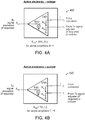
- FIGS. 4A - 4D illustrate four different differencing devices 210 ( FIG. 2 ).
- FIG. 4A illustrates an active electronic differencing device 400 that takes the difference of two voltages.
- FIG. 4B illustrates an active electronic differencing device 420 that takes the difference of two currents.
- These active differencing devices 400, 420 can be embodied in differential or balanced amplifiers.
- the active differencing devices 400, 420 typically provide gain, which is well known to be advantageous if it is desired to achieve a low noise figure for the receive signal.
- the active differencing devices 400, 420 can be realized with a wide range of input impedances. For example, voltage differencing devices typically present a high impedance whereas current differencing devices typically present a low impedance.
- This range of input impedances for the active differencing devices 400, 420 permits the active differencing device 400, 420 to be used with the matched impedance connection 300 as described in connection with FIG. 3A , the high impedance receive path signal connector 320 described in connection with FIG. 3B , or the high impedance transmit signal connector 340 described in connection with FIG. 3C .
- FIG. 4C illustrates a passive electronic differencing device 440.
- Passive devices are limited to having a gain less than one, and thus all have some loss. Consequently, passive differencing devices 440 have higher noise figures than the active electronic differencing devices 400, 420 described in connection with FIGS. 4A and 4B .
- There are many ways to implement a passive electronic differencing device For example, lumped element resistive dividers, traveling wave resistive (Wilkinson) dividers, and 180 degree hybrid couplers are all effective at implementing an electronic differencing device.
- the same physical hardware can realize both the matched signal connector described in connection with FIG. 3A 300 and the passive differencing device 440 which implements 180 degree phase reversal of the clean transmit signal where necessary as described in connection with FIG. 4C .
- FIG. 4D illustrates one embodiment of a photonic differencing device 460 that includes a balanced-drive optical modulator which produces a modulated output that is proportional to the sum or difference between the signals that are applied to the electrodes.
- Such electrodes can be either high impedance or matched impedance so that the photonic differencing device can be used with the matched impedance signal connector 300 described in connection with FIG. 3A , the high impedance receive path signal connector 320 described in connection with FIG. 3B or the high impedance transmit signal connector 340 described in connection with FIG. 3C .
- the photonic differencing device can have a gain that is greater or less than unity.
- the photonic differencing device can provide either gain or loss.
- the photonic differencing device is designed to have gain, it is capable of achieving low noise figure, much like active electronic differencing devices.
- the photonic differencing device is designed to have loss, it has higher noise figure, much like passive electronic differencing devices.
- Some types of differential optical modulators are only capable of summing two signals. In such cases, these differential modulators can realize the required differencing by offsetting the clean transmit signal by 180 degrees as described in connection with FIG. 4C .
- An ideal voltage source is a signal source with zero internal impedance.
- An ideal current source is a signal source with infinite internal impedance. Such ideal signal sources are not realizable.
- Realizable voltage sources generally have an internal impedance that is much lower than the external impedances in the circuit.
- Realizable current sources generally have an internal impedance that is much larger than the external impedances in the circuit.
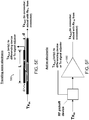
- FIG. 5 illustrates various signal isolators that can be used with the same-aperture any-frequency STAR system of the present teaching.
- FIG. 5A illustrates an electronic voltage-source-based isolator 500.
- the isolator 500 in FIG. 5A shows one simple way that isolation can be achieved with a voltage source.
- a voltage source establishes a potential difference or voltage across its output terminals. The voltage across a voltage source is independent of an external signal that is applied to its output. Hence the current that is developed through a resistor connected in series with a voltage source will not change the output voltage of the voltage source.
- the voltage source signal is the transmit signal and the externally applied signal would be the receive signal. Consequently, the output of the voltage source will contain a clean copy of the transmit signal, which is what is desired.
- FIG. 5B illustrates a current-source-based signal isolator 520 that can be used with the same-aperture any-frequency STAR system of the present teaching.
- Current sources establish a current that is independent of an external signal applied to its output. Hence, the current through a current source contains only the current source signal and will not contain any signal that corresponds to the externally applied signal.
- the current source signal is the transmit signal and the externally applied signal is the receive signal. Consequently, the output of the current source will contain a clean copy of the transmit signal, which is what is desired.
- FIG. 5C illustrates a non-reciprocal RF isolator 540 that can be used with the apparatus of the present teaching.
- non-reciprocal RF isolators are ferrite isolators and gyrators. These devices have low transmission loss in one direction and high transmission loss in the other direction. For example, there can be low transmission loss from port 1 to port 2, but high transmission loss in the other direction, from port 2 to port 1.
- FIG. 5D illustrates a photonic isolator 560 that can be used with the same-aperture any-frequency STAR system according to the present teaching.
- Photonic isolators provide good coupling in the forward coupling direction and high isolation in the reverse direction. Good coupling in the forward direction is accomplished by an electrical-to-optical conversion device, such as a diode laser or an optical modulator, whose optical output is efficiently coupled to an optical-to-electrical conversion device, such as a photodetector.
- Photonic isolators provide extremely low coupling in the reverse direction because devices such as photodetector do not emit light, and the electrical-to-optical conversion device is not capable of detecting light.
- a directional coupler 580 is used to perform the isolation as shown in Fig. 5E .
- a directional coupler uses the traveling wave property. By having a 2 nd electrode of the proper length, L, and locating it a proper distance, d, away from a first electrode, a portion of the power traveling in the first electrode will couple over into the 2 nd electrode. Since this is a reciprocal device, RF power traveling in the opposite direction in the first electrode will also be coupled into the 2 nd electrode and this power is dissipated into a load as shown.
- RF isolation can also be achieved in RF amplifiers in which the reverse isolation is greater than the forward gain.
- An isolation technique that takes advantage of such an amplifier 590 is shown in FIG. 5F .
- some form of RF pickoff device is needed, such as an RF splitter or a directional coupler.
- FIGS. 6A-6D illustrate signal processors 600, 620, 640, and 660 that can be used with the same-aperture any-frequency STAR system according to the present teaching.
- Various types of digital and/or analog signal processors 600, 620, 640, and 660 can be used as shown in FIGS. 6A-6D .
- the signal processors 600, 620, 640, and 660 execute a wide range of algorithms, such as a least mean square algorithm, to perform various functions.
- the signal processing can be performed at the radio-frequency (RF) of the transmit and the receive signals, or at some lower intermediate-frequency (IF) signals, using well known techniques for converting the RF signals to IF signals.
- RF radio-frequency
- IF intermediate-frequency
- One such function is to correlate the clean copy of the transmit signal with the output of the differencing device 210, which contains both receive and transmit signals. The result of this correlation will be a residual transmit signal that is present in the output of the differencing device 210.
- Another function performed by the signal processor 212 is estimating the complex value of the transmit signal that needs to be applied to the input of the differencing device 210 so as to result in minimizing the residual transmit signal at the output of the differencing device 210.
- the result of this estimation is a signal that is applied to the transmit signal adjustment circuit 214.
- FIG. 7 illustrates transmit signal adjustment circuits 700, 720 that can be used with the same-aperture any-frequency STAR system according to the present teaching.
- the transmit signal adjustment circuits 700, 720 make adjustments, determined by the signal processor, to the complex value of the transmit signal.
- the signal adjuster can adjust upon either the transmit signal at RF frequencies or at its down-converted IF frequencies. If the signal adjuster operates at the IF frequencies, then the adjuster will need to be followed by a frequency up-converter, using one of numerous known techniques for frequency up-conversion.
- FIGS 7A and B There are numerous types of signal adjustment circuits that can be used with the same-aperture any-frequency STAR system according to the present teaching, two of which are shown in FIGS 7A and B.
- FIG 7A illustrates an embodiment of an adjustment circuit 700 that adjusts the magnitude and phase of the transmit signal.
- FIG 7B illustrates an embodiment of an adjustment circuit 720 that adjusts the in-phase in-quadrature components of the transmit signal.
- FIG. 8 illustrates a block diagram of a front-end system 800 that includes the matched impedance signal connector 802, the photonic differencing circuit 804 and the voltage-source isolator 806 as described herein.
- the system 800 passively reduces and ultimately even eliminates the need for the transmit signal adjustment device and the signal processor described herein.
- the circuits on the two sides of the differencing device 804 are made as identical as possible.
- a pseudo-antenna 808 can be constructed, which is a circuit that replicates as closely as possible the impedance vs. frequency function of the antenna 810.
- the matched impedance type can be used.
- This example system uses the photonic differencing device described herein. Key advantages of this type of differencing device or subtractor are that they are extremely wide bandwidth (> 4 decades) and there is high isolation between the + and - differencing ports. Voltage source isolation, with identical output impedance in the two outputs, further enhances the balance.
- One of the disadvantages of this system architecture is the relatively high loss incurred by the transmit signal. Because the same transmit power is supplied to both the antenna and the pseudo-antenna, there is 3 dB of loss for ideal (i.e., lossless) connectors. There is an additional 3 dB loss at each of the connectors. Thus, the total transmit loss between the output of the power amplifier and the antenna is 6 dB plus the excess loss of the connector.
- FIG. 9 illustrates a block diagram of one exemplary embodiment of a front-end system 900 that includes the signal connector 902 to which a high impedance is presented by the output of the transmit signal path, the passive electronic differencing device 904, and the current-source-based isolator 906 described herein.
- This is compatible with the version of the connector that has a high impedance on the port that connects to the transmit path output.
- the impedances on the other two connector ports are matched: the antenna port provides the load to the antenna 908 and the differencing port is loaded by one input to the differencing device 904, which in this system 900 is of the passive electronic type.
- the passive electronic differencing device 904 has a narrower bandwidth than the photonic differencing device described herein. However, it has slightly lower transmit loss: 4.77 dB ideally, vs. 6 dB for the architecture shown in FIG. 8 .
- FIG. 10 illustrates a block diagram of one exemplary embodiment of a front-end system 1000 that includes a signal connector 1002 with a high impedance applied to the output receive signal port by the '+' port of the active electronic differencing device 1004, and the voltage-source-based isolator 1006 described herein.
- differencing devices 1004 of this type are that the input impedance can be made higher than the system impedance.
- a common system impedance is 50 ⁇ .
- the input impedance of the active electronic differencing device 1004 can range from 500 ⁇ for some implementations to > 1 M ⁇ for other implementations. This means that the signal power drawn by the differencing device inputs can be negligible.
- the system configuration that is shown in FIG. 10 contains both a voltage source isolator 1006 and a signal connector 1002 with high impedance at its differencing device port.
- the transmit loss is now 0 dB, at least in the ideal case.
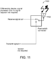
- FIG. 11 shows a same-aperture any-frequency STAR system 1100 using a fast switch as a signal connector.
- the configuration leads to a particularly simple implementation of the present teaching.
- the basis of operation of this implementation can be understood as follows. It is well known to those in the art that a continuous signal can be completely characterized by sampling it at a rate that is at least twice its maximum frequency component. This is often referred to as the Nyquist sampling theorem.
- Nyquist sampling One of the consequences of Nyquist sampling is that it is not necessary to continuously monitor a continuous signal: observing - i.e., sampling - a continuous signal at its Nyquist rate is sufficient. Instantaneous sampling - i.e. in zero time - is obviously a theoretical abstraction.
- a sample is considered to be instantaneous if the length of the sampling interval is short compared to the interval between samples. For example, a sampling pulse that lasts for even 1% of the time interval between samples is often considered as sufficiently short that it approximates the theoretically ideal sampling.
- the fast switch connector 1100 utilizes the inter-sampling interval to connect the transmitter to the antenna 1102. There is negligible transmitter power loss since the transmitter is connected to the antenna 1102 for almost 100 % of the time. With the fast switch signal connector, the transmitter and the receiver are never simultaneously connected to the antenna 1102. Hence, the transmit signal does not have the opportunity to enter the receive path. This can eliminate the need for the differencing device, isolator, signal processor and transmit signal adjuster described herein for some applications
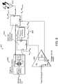
- FIG. 12 shows a block diagram of a same-aperture any-frequency STAR system 1200 using digital signal processing 1202 to augment the example front end system shown in FIG. 10 .
- This example system uses the digital signal processor with down conversion described in connection with FIG. 6B .
- this example system uses the vector modulator type of transmit signal adjuster described in connection with FIG. 7B .
- a portion of the output of the differencing device is fed to a downconverter 1206 that translates the frequency spectrum of the signal down to a lower frequency, which can be an intermediate frequency (IF). Alternatively, it can be translated all the way down to zero frequency, which is more commonly referred to as baseband.
- IF intermediate frequency
- a portion of the transmit signal is also downconverted, with the constraint that it is converted to the same frequency to which the output of the differencing device was converted. Once both of these signals have been downconverted, they are converted to digital form via analog-to-digital converters (ADC) 1204.
- ADC analog-to-digital converters
- the digital signal processor 1202 is used to correlate the transmit signal with the differencing device 1208 output to isolate the residual transmitter component in the differencing device 1208 output.
- the signal processor 1202 then forms an estimate of the optimum complex value of the transmitter signal that needs to be injected into the differencing device 1208 so as to minimize the residual transmitter signal that is present at the differencing device 1208 output.
- the output of the signal processor 1202 includes two signals that contain the desired settings on the IQ transmit signal adjuster 1212. Since in the example shown in FIG. 12 , we are using a vector modulator as the IQ transmit signal adjuster 1212, the complex settings are for the in-phase (I) and quadrature (Q) portions of the transmitter signal. Since many vector modulators require analog inputs, FIG. 12 shows digital-to-analog converters (DACs) 1210 to execute the required conversion.
- DACs digital-to-analog converters
- FIG. 12 shows the IQ transmit signal adjuster 1212 operating on the Tx signal at RF frequencies using the complex settings supplied by the adapative signal processor 1202 and DACs 1210. It is also possible for an adaptive signal processor and DAC to generate the adjusted transmit signal itself at IF frequencies, and to up-convert it to RF frequencies, as will be shown in FIG. 21 below along with the advantages of that approach. Operating on the Tx signal at RF frequencies as shown in FIG. 12 , however, is significantly simpler because it obviates the need for frequency up-conversion.
- FIG. 13 shows a block diagram of a same-aperture any-frequency STAR system 1300 illustrating how analog signal processing could be used to augment the example front end system shown in FIG. 10 .
- the analog signal processor 1302 without frequency conversion as described in connection with FIG. 6C . Since the transmitter and differencing device outputs are analog signals, the analog signal processor 1302 does not require analog-to-digital converters.
- One way that the required processing can be performed is with an integrated circuit that contains many of the functions, such as the AD8333, which is a dual I/Q demodulator commercially available from Analog Devices.
- the required analog multiplications also can be performed with integrated circuits, such as the AD835, which is a voltage-output, 4-quadrant multiplier also commercially available from Analog Devices.
- the output of the analog multipliers with appropriate summing, scaling and integration, can drive the vector modulator inputs directly without the need for digital-to-analog coverers.
- the two versions of the transmit signal arriving at the subtractor 210 inputs are processed to have the same delay. This can be accomplished by inserting a delay in path 206 that matches the delays through the subtractor + signal processor + Tx signal adjuster 214 + frequency conversions (if used). However, in some of these methods of operation, it is relatively difficult to accurately provide the two versions of the transmit signal at the subtractor 210 inputs with the same delay.
- the operating conditions are such that there is a large reflection of the transmit signal near the antenna 204, then at the output of the connector 202 there will be two copies of the Tx signal that need to be cancelled: one copy that is reflected at the input to the antenna and the other copy that is reflected off an object near the antenna 204.
- FIG. 21 illustrates a system 2100 according to the present teaching for providing multiple, appropriately delayed copies of the transmit signal to the subtractor.
- the system described in FIG. 21 is similar to the same-aperture any-frequency STAR system 1200 using digital signal processing 1202 that was described in connection with FIG. 12 .
- the system 2100 includes the active electronic differencing device 1208, down converters 1206, and analog-to-digital converters 1204 in the system 1200.
- the adaptive signal processor 1202 also includes a means for generating multiple delayed copies of the Tx signal.
- the adaptive signal processor 1202 is electrically connected to a digital-to-analog converter 1210 that is electrically connected to an up converter 2102 and then to the active electronic differencing device 1208.
- the Tx signal is down-converted and run through the analog-to-digital converter 1204 and then stored in the signal processor 1202.
- the analog-to-digital converter 1204 In this way, multiple, appropriately-delayed copies of the Tx signal can be generated in the digital domain and the resulting signals can be converted back by a digital-to-analog converter 1210 to an analog signal which is then up-converted by a frequency converter, such as a mixer.
- the up-conversion can be performed digitally and then fed to a digital-to-analog converter.
- One powerful aspect of this approach is that the appropriate delays for each copy of the transmit signal can be determined by signal processing using well know techniques. The delays can be updated as signal conditions change.
- All of the embodiments of the present teaching in FIGS. 2-13 would be effective at removing the high-power transmit signal from the receive path. If the transmit signal strength is only of the same order of magnitude as, or smaller in magnitude than, the receive signal, then much less hardware may be required.
- FIG. 14 illustrates a subset system 1400 of hardware in the same-aperture any-frequency STAR system described in connection with FIG. 2 that is useful for some embodiments when the transmit signal strength is only as strong as or weaker than the receive signal.
- a three-port signal connector 1402 is necessary to permit connection of the separate transmit path 1404 and receive signal path 1406 to the antenna 1408, and the isolator 1410 is necessary to shield the transmit path 1404 from the signal environment in which the antenna operates.
- the three-port signal connector 1402 is a ferrite circulator.
- An analog signal differencing device may not be required, and thus neither would the transmit signal adjuster be required. Because the transmit signal is relatively small, it does not saturate any of the components in the receive signal path, and its removal from the receive signal path, if deemed necessary, can be accomplished using well-known digital signal processing techniques.
- the transmit signal may be differentiated from the receive signal in two key aspects: (1) the transmit signal is much more powerful than the receive signal and (2) the transmit signal does not need to be demodulated to recover the information, if any, that is being conveyed by the transmit signal.
- the large signal needs to be removed so that the receiver can process, i.e. demodulate, the desired receive signal(s).
- Various means of removing co-site and jamming signals are well known.
- One common approach is to use RF filters to suppress the large signal while permitting the receive signal(s) to pass.
- Such techniques are effective, of course, only when the receive and co-site/jamming signals occupy disjoint frequency bands.
- the teaching of the present invention will now be applied to suppress co-site and jamming signals, where the frequency spectra of the receive and co-site/jamming signals may overlap.
- FIG. 15 illustrates one exemplary system 1500 which is an embodiment of the system 1400 in FIG. 14 , including a signal connector 1502 to which a high impedance is presented by the output of the photonic isolator 1504 in the transmit signal path 1506, and in which a conventional digital signal processor 1508 is used to remove the transmit signal from the receive path 1510 after all signals are frequency down-converted and then converted from the analog to digital domain.
- a reference copy of the interferers that is fed to the interference canceller must be self-generated. Except for the fact that problematic interferers are large in amplitude relative to the signal of interest (SOI), we often cannot assume we know anything else about these interferers at all.
- SOI signal of interest
- a known method to preferentially detect the interfering source is to use directional antennas whose maximum sensitivity is pointed in the direction of the interfering source.
- the effectiveness of such techniques, however, is heavily dependent on the directionality of the antenna beam and the angle separation between the interfering source and the SOI. Therefore, one feature of the present teaching is an approach for extracting a reference copy of a strong interfering signal from the composite SOI + interfering signal stream that is coming from an antenna.
- FIG. 16 illustrates a system 1600 that generates a reference copy of an interfering signal according to the present teaching.
- a portion of the antenna 1602 output is tapped off and fed to an N-bit quantizer 1604, where N is sufficient to quantize the strong interferer but not sufficiently large to also quantize the SOI, which is much smaller than the interfering signal.
- the N-bit quanitzer serves as a sort of a reverse limiter, letting only large signals through and suppressing smaller signals.
- the delay involved in producing a reference copy of the interferers in this way and processing it in the interference canceller can be reproduced in the signal path leading from the antenna 1602 to the interference canceller as shown in FIG. 16 .
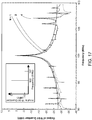
- simulations were performed, in which the "high-power" interferer was a 1-V sine wave at 100 MHz and the "low power” SOI was a 0.1-V sine wave at 107 MHz.
- FIG. 17 illustrates results of a simulation of the architecture in FIG. 16 , whereby the output of a 1-bit quantizer produces a copy of the high-power interferer at 100 MHz, allowing its subtraction from the lower-power 107-MHz SOI in a differencing device.
- the plots illustrated in FIG. 17 show the input to the N-bit quantizer, while the main plot shows the output of the quantizer, with the number of bits as a parameter.
- the interferer only a factor of 10 times stronger than the SOI, a single bit of quantization "passes" the large interferer and completely fails to sense the smaller SOI, and 4 bits are sufficient to completely sense both the interferer and SOI. With 2 bits, the SOI is ⁇ 20 dB below the high-power interferer.
- FIG. 18 is a plot that shows the relationship between the signal-to-interferer ratio at the antenna to the number of bits of quantization that we can use without having to worry about suppressing the SOI, which is like throwing the SOI "baby” out with the interferer(s) "bathwater.”
- the number of bits is a metric of the complexity of the interference signal spectrum.
- FIG. 19 illustrates a block diagram of a system 1900 according to the present teaching that uses a self-generated reference in an interference canceller.
- the system 1900 includes the N-bit quantizer 1902 that generates the reference copy of the interferer as described in connection with FIG. 16 .
- An analog processor 1904 and a digital processor 1906 are used in a feedback loop with the large signal differencing device 1908 to remove the interfering signal.
- An RF delay 1910 is used to match the delay between the + and - ports of the differencing device 1908.
- FIGS. 2-19 relate to systems in which the transmitting and receiving antenna consists of one radiating element addressed by one front-end.
- the antenna symbol in FIGS 1 , 2 , 8-16 , and 19 can represent an array of radiating elements all being fed the same transmit signal by a single front-end and having their received signals combined for processing in that same front-end.
- each front-end may need to mitigate the effect of the presence in its receive signal path of not only the transmit signal being transmitted by its radiating element or small group of radiating elements, but also by the signals being transmitted by any or all of the other elements in the array whose transmitted signals will be received in part by this front-end's antenna element through a phenomenon known in the art as mutual coupling between antenna elements.
- FIG. 20 illustrates a system 2000 according to the present teaching for mitigating the effect of signals being transmitted not only by the antenna element 2002 attached to the front-end 2004 shown by the collection of hardware inside dashed box but also by the N - 1 other radiating elements in an array of N such radiating elements.
- the system 2000 is a generalized form of the single-element front-end described in connection with FIG. 2 .
- the difference between the two figures is noticeable in that there are now a number N rather than only one transmit signal adjuster. That is one for each of the N elements in the antenna array.
- the copy of the transmit signal which, in the single-antenna-system front-end of FIG. 2 , the isolator 2004 provides to a single transmit signal adjuster 2006, is now split into N parts by an N-way RF divider 2008, such as two-way traveling-wave resistive power dividers (Wilkinson dividers) employed in a corporate tree arrangement to yield N-way splitting of the signal.
- N-way RF divider 2008 such as two-way traveling-wave resistive power dividers (Wilkinson dividers) employed in a corporate tree arrangement to yield N-way splitting of the signal.
- One of the N attenuated (by at least a factor of N) copies of the transmit signal is fed to this front-end's transmit signal adjuster 2006 exactly as was done in FIG. 2 .
- the remaining N - 1 attenuated copies of this front-end's transmit signal are routed out of this front-end, and each is connected to one of the transmit signal adjusters 2006 in each of the N - 1 other antenna element 2002 front-ends 2004.
- each of the other N - 1 transmit signal adjusters 2006 in the one element's front-end 2004 shown in FIG. 20 receives an attenuated copy of the signal being transmitted by the other N - 1 antenna elements 2002.
- These signal adjuster's 2006 outputs are combined, along with the output of the transmit signal adjuster 2006 that acts upon this antenna element's transmit signal, in an N-way RF combiner 2010, as shown in FIG. 20 .
- this N-way RF combiner 2010 may consist, for example, of two-way traveling-wave resistive power combiners (Wilkinson power combiners) employed in a corporate tree arrangement to yield N-way combining of the RF signals.
- the combined copies of the transmit signals are subtracted from the signal received by this front-end's antenna element 2002 in the differencing device 2012.
- the output of the differencing device 2012 is fed to a signal processor 2014.
- the signal processor 2014 receives its own attenuated copy of each element's transmit signal as the signal processor in FIG. 2 does. For clarity, however, this feature is not shown in FIG. 20 , but will be understood by those skilled in the art.
Landscapes
- Engineering & Computer Science (AREA)
- Computer Networks & Wireless Communication (AREA)
- Signal Processing (AREA)
- Physics & Mathematics (AREA)
- General Physics & Mathematics (AREA)
- Radar, Positioning & Navigation (AREA)
- Remote Sensing (AREA)
- Transceivers (AREA)
- Transmitters (AREA)
Claims (15)
- System für gleichzeitiges Senden und Empfangen bei gleicher Apertur und einer beliebigen Frequenz (200), das System umfassend:a. einen Signalverbinder (202), der einen mit einer Antenne (204) elektrisch gekoppelten ersten Anschluss, einen mit einem Sendesignalpfad (205) elektrisch gekoppelten zweiten Anschluss und einen mit einem Empfangssignalpfad (206) elektrisch gekoppelten dritten Anschluss aufweist, wobei der Signalverbinder (202) eingerichtet ist, um ein Sendesignal in dem Sendesignalpfad (205) zu der Antenne (204) und ein Empfangssignal in dem Empfangssignalpfad (206) zu leiten;b. einen Signalisolator (208), der in dem Sendesignalpfad (205) positioniert ist und der eingerichtet ist, um einen Restteil des Empfangssignals von dem Sendesignalpfad (205) zu entfernen, wobei ein Ausgang des Signalisolators (208) eingerichtet ist, um einen Teil des Sendesignals, bei dem der Restteil des Empfangssignals entfernt wurde, bereitzustellen; undc. eine Signaldifferenzierungsvorrichtung (210), die einen mit dem Sendesignalpfad (205) elektrisch gekoppelten ersten Eingang und einen mit dem dritten Anschluss des Signalverbinders (202) elektrisch gekoppelten zweiten Eingang aufweist, wobei die Signaldifferenzierungsvorrichtung (210) eingerichtet ist, um einen Teil des Sendesignals, bei dem der Restteil des Empfangssignals entfernt wurde, in dem Empfangssignalpfad (206) zu subtrahieren, wodurch eine genauere Kopie des Empfangssignals bereitgestellt wird;wobei das Sendesignal und das Empfangssignal ein gleiches Signalfrequenzband zu einer gleichen Zeit einnehmen.
- System nach Anspruch 1, wobei der Signalverbinder (202) eingerichtet ist, um bereitzustellen:eine angepasste Impedanz für zumindest einen von dem ersten, zweiten und dritten Anschluss; odereine höhere Impedanz an dem zweiten Anschluss als entweder an dem ersten oder dem zweiten Anschluss.
- System nach Anspruch 1 oder 2, wobei:der Signalverbinder (202) einen schnellen Schalter umfasst; und/oderdie Signaldifferenzierungsvorrichtung (210) ausgewählt ist aus der Gruppe bestehend aus einer aktiven Differenzierungsvorrichtung, einer passiven Differenzierungsvorrichtung und einer photonischen Differenzierungsvorrichtung; und/oderder Isolator (208) ausgewählt ist aus der Gruppe bestehend aus einem auf einer Spannungsquelle basierenden elektronischen Isolator, einem auf einer Stromquelle basierenden Signalisolator, einem nicht-reziproken HF-Isolator und einem photonischen Isolator.
- System nach Anspruch 1, 2 oder 3, weiter umfassend einen Signalprozessor (212), der einen mit dem Ausgang der Signaldifferenzierungsvorrichtung (210) gekoppelten Eingang aufweist, wobei der Signalprozessor (212) eingerichtet ist, um eine Kopie des Sendesignals mit dem Ausgang der Differenzierungsvorrichtung (210) zu korrelieren und um eine genauere Darstellung des Empfangssignals zu erzeugen.
- System nach Anspruch 4, wobei der Signalprozessor (212) eingerichtet ist, um ein Signal zu erzeugen, das, wenn es zu dem Teil des Sendesignals von dem Isolator (208) hinzugefügt wird, vollständiger Restteile des Sendesignals von dem resultierenden Differenzsignal subtrahiert.
- System nach Anspruch 4 oder 5, wobei der Signalprozessor (212) ausgewählt ist aus der Gruppe bestehend aus einem analogen Signalprozessor und einem digitalen Signalprozessor.
- System nach einem der vorstehenden Ansprüche, weiter umfassend ein Rückkopplungssystem, das einen mit dem Ausgang der Signaldifferenzierungsvorrichtung (210) gekoppelten Eingang und einen mit dem ersten Eingang der Signaldifferenzierungsvorrichtung (210) gekoppelten Ausgang aufweist, wobei das Rückkopplungssystem eingerichtet ist, um ein Signal zu erzeugen, das, wenn es zu dem Teil des Sendesignals von dem Isolator (208) hinzugefügt wird, vollständiger das Sendesignal von dem Empfangssignal subtrahiert.
- System nach Anspruch 7, wobei das Rückkopplungssystem einen Signalprozessor und eine Sendesignal-Einstellschaltung umfasst.
- System nach Anspruch 7 oder 8, wobei das Rückkopplungssystem eingerichtet ist, um an dem Ausgang einen gewünschten komplexen Wert des Sendesignals zu erzeugen, der, wenn er zu dem Teil des Sendesignals von dem Isolator (208) hinzugefügt wird, vollständiger das Sendesignal von dem Empfangspfad subtrahiert.
- Verfahren für gleichzeitiges Senden und Empfangen bei gleicher Apertur und einer beliebigen Frequenz, das Verfahren umfassend:a. Verbinden eines Empfangssignals von einer Antenne (204) mit einem Sendesignal von einem Sendesignalpfad (205), sodass das Empfangssignal zu einem Empfangssignalpfad (206) geleitet wird und das Sendesignal von dem Sendesignalpfad (205) zu der Antenne (204) geleitet wird;b. Isolieren eines Teils des Sendesignals von einer Empfangsrestsignalkomponente in dem Sendesignalpfad (205); undc. Subtrahieren des isolierten Teils des Sendesignals in dem Sendesignalpfad (205) von dem Empfangssignal in dem Empfangssignalpfad (206), wodurch ein Restteil des gesendeten Signals von dem Empfangssignalpfad (206) entfernt wird, wobei eine genauere Darstellung des Empfangssignals hergestellt wird;wobei das Sendesignal und das Empfangssignal ein gleiches Signalfrequenzband zu einer gleichen Zeit einnehmen.
- Verfahren nach Anspruch 10, wobei das Verbinden des Empfangssignals von der Antenne (204) mit dem Sendesignal von dem Sendesignalpfad (205) ein schnelles Schalten umfasst.
- Verfahren nach Anspruch 10 oder 11, wobei das Isolieren nicht-reziprok durchgeführt wird.
- Verfahren nach Anspruch 10, 11 oder 12, wobei das Isolieren unter Verwendung photonischer Isolation durchgeführt wird.
- Verfahren nach einem der Ansprüche 10 bis 13, wobei das Subtrahieren des isolierten Teils des Sendesignals in dem Sendesignalpfad (205) von dem Empfangssignal in dem Empfangssignalpfad (206) unter Verwendung photonischer Subtraktion oder elektronischer Subtraktion durchgeführt wird.
- Verfahren nach einem der Ansprüche 10 bis 14, weiter umfassend Korrelieren einer Kopie des Sendesignals in dem Sendesignalpfad (205) mit dem subtrahierten Signal, um eine genauere Darstellung des Empfangssignals zu erzeugen.
Priority Applications (1)
| Application Number | Priority Date | Filing Date | Title |
|---|---|---|---|
| EP18202965.2A EP3461011A1 (de) | 2012-07-30 | 2013-07-30 | Kommunikationssystem und -verfahren für gleichzeitiges senden und empfangen bei gleicher apertur und einer beliebigen frequenz |
Applications Claiming Priority (4)
| Application Number | Priority Date | Filing Date | Title |
|---|---|---|---|
| US201261677366P | 2012-07-30 | 2012-07-30 | |
| US201361755044P | 2013-01-22 | 2013-01-22 | |
| US13/844,180 US9935680B2 (en) | 2012-07-30 | 2013-03-15 | Same-aperture any-frequency simultaneous transmit and receive communication system |
| PCT/US2013/052649 WO2014022348A1 (en) | 2012-07-30 | 2013-07-30 | Same-aperture any-frequency simultaneous transmit and receive communication system |
Related Child Applications (2)
| Application Number | Title | Priority Date | Filing Date |
|---|---|---|---|
| EP18202965.2A Division EP3461011A1 (de) | 2012-07-30 | 2013-07-30 | Kommunikationssystem und -verfahren für gleichzeitiges senden und empfangen bei gleicher apertur und einer beliebigen frequenz |
| EP18202965.2A Division-Into EP3461011A1 (de) | 2012-07-30 | 2013-07-30 | Kommunikationssystem und -verfahren für gleichzeitiges senden und empfangen bei gleicher apertur und einer beliebigen frequenz |
Publications (3)
| Publication Number | Publication Date |
|---|---|
| EP2880771A1 EP2880771A1 (de) | 2015-06-10 |
| EP2880771A4 EP2880771A4 (de) | 2016-04-06 |
| EP2880771B1 true EP2880771B1 (de) | 2018-12-12 |
Family
ID=50028466
Family Applications (2)
| Application Number | Title | Priority Date | Filing Date |
|---|---|---|---|
| EP18202965.2A Pending EP3461011A1 (de) | 2012-07-30 | 2013-07-30 | Kommunikationssystem und -verfahren für gleichzeitiges senden und empfangen bei gleicher apertur und einer beliebigen frequenz |
| EP13825058.4A Active EP2880771B1 (de) | 2012-07-30 | 2013-07-30 | Kommunikationssystem für gleichzeitiges senden und empfangen bei gleicher apertur und einer beliebigen frequenz |
Family Applications Before (1)
| Application Number | Title | Priority Date | Filing Date |
|---|---|---|---|
| EP18202965.2A Pending EP3461011A1 (de) | 2012-07-30 | 2013-07-30 | Kommunikationssystem und -verfahren für gleichzeitiges senden und empfangen bei gleicher apertur und einer beliebigen frequenz |
Country Status (6)
| Country | Link |
|---|---|
| US (4) | US9935680B2 (de) |
| EP (2) | EP3461011A1 (de) |
| JP (1) | JP5890069B2 (de) |
| KR (3) | KR102014929B1 (de) |
| CN (2) | CN104584445B (de) |
| WO (1) | WO2014022348A1 (de) |
Cited By (1)
| Publication number | Priority date | Publication date | Assignee | Title |
|---|---|---|---|---|
| US11539392B2 (en) | 2012-07-30 | 2022-12-27 | Photonic Systems, Inc. | Same-aperture any-frequency simultaneous transmit and receive communication system |
Families Citing this family (15)
| Publication number | Priority date | Publication date | Assignee | Title |
|---|---|---|---|---|
| US9209840B2 (en) | 2012-07-30 | 2015-12-08 | Photonic Systems, Inc. | Same-aperture any-frequency simultaneous transmit and receive communication system |
| US10374656B2 (en) | 2012-07-30 | 2019-08-06 | Photonic Systems, Inc. | Same-aperture any-frequency simultaneous transmit and receive communication system |
| US9985772B1 (en) | 2015-01-30 | 2018-05-29 | The Charles Stark Draper Laboratory, Inc. | Digital simultaneous transmit and receive communication system |
| US9893435B2 (en) * | 2015-02-11 | 2018-02-13 | Kymeta Corporation | Combined antenna apertures allowing simultaneous multiple antenna functionality |
| US10128874B2 (en) * | 2015-08-28 | 2018-11-13 | Qorvo Us, Inc. | Radio frequency coupler circuitry |
| US10158432B2 (en) * | 2015-10-22 | 2018-12-18 | Photonic Systems, Inc. | RF signal separation and suppression system and method |
| US10623986B2 (en) | 2015-10-22 | 2020-04-14 | Photonic Systems, Inc. | RF signal separation and suppression system and method |
| US10649067B1 (en) * | 2016-10-26 | 2020-05-12 | Northrop Grumman Systems Corporation | Simultaneous transmit and receive (STAR) subsystem with external noise canceller |
| US11356235B2 (en) | 2017-05-24 | 2022-06-07 | The Board Of Trustees Of The University Of Illinois | Self-interference cancellation for in-band full duplex single antenna communication systems |
| CN107317665B (zh) | 2017-06-22 | 2019-05-17 | 维沃移动通信有限公司 | 一种同时同频全双工系统及移动终端 |
| EP3688877B1 (de) * | 2017-09-26 | 2023-09-13 | Photonic Systems, Inc. | Einkanaliges vollzeit-vollduplex-drahtlossignalübertragungssystem |
| US10819401B2 (en) | 2018-01-19 | 2020-10-27 | Photonic Systems, Inc. | System to acquire channel state information for multiple-input and multiple-output systems |
| US10554246B2 (en) | 2018-03-30 | 2020-02-04 | Intel Corporation | Method and apparatus for broadband high-isolation circulator for simultaneous transmit and receive systems |
| US10693564B2 (en) | 2018-10-04 | 2020-06-23 | Raytheon Company | Photonics interference canceler |
| CN114826322B (zh) * | 2022-06-27 | 2022-09-02 | 中国人民解放军国防科技大学 | 一种能量选择自适应非互易二端口器件 |
Family Cites Families (72)
| Publication number | Priority date | Publication date | Assignee | Title |
|---|---|---|---|---|
| US670434A (en) * | 1900-06-18 | 1901-03-26 | Louis T Rector | Reach-coupling. |
| GB848113A (en) | 1957-08-20 | 1960-09-14 | Gen Electric Co Ltd | Improvements in or relating to electromagnetic wave switching arrangements |
| JPS5328680B2 (de) | 1971-10-12 | 1978-08-16 | ||
| JPS5850193B2 (ja) | 1976-08-30 | 1983-11-09 | 三菱重工業株式会社 | ラジアルタイヤ用グリ−ンケ−ス製造装置 |
| JPS57197934A (en) | 1981-05-29 | 1982-12-04 | Fujitsu Ten Ltd | Radio transmitter and receiver |
| FR2574943B1 (fr) | 1984-12-18 | 1987-05-22 | Thomson Csf | Systeme analyseur de transitoires |
| US4801901A (en) | 1987-03-13 | 1989-01-31 | Hittite Microwave Corporation | Non-ferrite non-reciprocal phase shifter and circulator |
| JP2712379B2 (ja) | 1988-09-30 | 1998-02-10 | 日本電気株式会社 | 無線機 |
| CA2011954C (en) | 1989-03-14 | 1994-02-22 | Hiroshi Hamano | Optical modulator |
| US5287212A (en) | 1989-09-07 | 1994-02-15 | Cox Charles H | Optical link |
| EP0459571B1 (de) | 1990-05-29 | 1995-09-20 | Laboratoires D'electronique Philips | Langsam-Wellen-Mikrostreifenübertragungsleitung und Anordnung mit einer solchen Leitung |
| US5303079A (en) | 1992-04-09 | 1994-04-12 | At&T Bell Laboratories | Tunable chirp, lightwave modulator for dispersion compensation |
| US6337660B1 (en) | 1993-09-17 | 2002-01-08 | The United States Of America As Represented By The Secretary Of The Navy | Fiber optic true time-delay array antenna feed system |
| US5389782A (en) | 1994-05-13 | 1995-02-14 | The United States Of America As Represented By The Secretary Of The Navy | Optically powered amplifier used by an electromagnetic field sensor to amplify an electrical signal from an antenna |
| JPH0879126A (ja) | 1994-09-05 | 1996-03-22 | Tech Res & Dev Inst Of Japan Def Agency | 同一周波数同時送受信用空中線接続器 |
| JPH098737A (ja) | 1995-06-23 | 1997-01-10 | Tokin Corp | 受信システム |
| US5602387A (en) | 1995-06-26 | 1997-02-11 | The United States Of America As Represented By The Secretary Of The Air Force | Method of protecting an RF receiver in a hostile electromagnetic environment |
| DE19649085A1 (de) | 1996-11-27 | 1998-05-28 | Alsthom Cge Alcatel | Sende-/Empfangseinrichtung und Verfahren zum Übertragen von breitbandigen Signalen sowie Sende-/Empfangseinrichtung zum Empfang von breitbandigen Signalen |
| US5977911A (en) | 1996-12-30 | 1999-11-02 | Raytheon Company | Reactive combiner for active array radar system |
| US6295395B1 (en) | 1997-01-31 | 2001-09-25 | The United States Of America As Represented By The Secretary Of Commerce | True time delay generation utilizing broadband light source with fiber chirp grating array and acousto-optic beam steering and 2-D architectures |
| JPH1152313A (ja) | 1997-08-08 | 1999-02-26 | Mitsubishi Electric Corp | 光変調装置 |
| JP3011164B2 (ja) * | 1997-11-14 | 2000-02-21 | 日本電気株式会社 | レーダ装置 |
| US6393177B2 (en) | 1998-01-20 | 2002-05-21 | United States Of America | True time delay generating system and method |
| US6137442A (en) | 1998-04-01 | 2000-10-24 | The United States Of America As Represented By The Secretary Of The Navy | Chirped fiber grating beamformer for phased array antennas |
| JPH11308143A (ja) | 1998-04-21 | 1999-11-05 | Sony Corp | 通信装置 |
| US6081232A (en) | 1998-07-06 | 2000-06-27 | The United States Of America As Represented By The Secretary Of The Army | Communication relay and a space-fed phased array radar, both utilizing improved mach-zehnder interferometer |
| US6175672B1 (en) | 1999-06-18 | 2001-01-16 | Raytheon Company | RF wide bandwidth lossless high performance low noise transmissive link |
| JP2001036169A (ja) | 1999-07-23 | 2001-02-09 | Furukawa Electric Co Ltd:The | 双方向励起光増幅器 |
| US6330098B1 (en) | 1999-10-06 | 2001-12-11 | Codeon Corporation | Apparatus for externally modulating two optical channels at the same time |
| JP2003530685A (ja) | 1999-10-28 | 2003-10-14 | パワースマート,インク. | I2c光アイソレータ回路 |
| US6704349B1 (en) * | 2000-01-18 | 2004-03-09 | Ditrans Corporation | Method and apparatus for canceling a transmit signal spectrum in a receiver bandwidth |
| US7187907B2 (en) | 2000-05-09 | 2007-03-06 | Bernard Widrow | Simultaneous two-way transmission of information signals in the same frequency band |
| US6320539B1 (en) | 2000-06-09 | 2001-11-20 | The United States Of America As Represented By The Secretary Of The Navy | Fiber-optic, wideband array antenna beamformer |
| US20020106141A1 (en) | 2001-02-08 | 2002-08-08 | Codeon Corporation | Low-loss electrode designs for high-speed optical modulators |
| US6580843B2 (en) | 2001-04-05 | 2003-06-17 | Fujitsu Limited | Optical device |
| US6934476B2 (en) | 2001-08-31 | 2005-08-23 | The Boeing Company | Cosite interference rejection system using an optical approach |
| US7346012B2 (en) | 2002-12-13 | 2008-03-18 | Tioga Technologies Ltd. | Transceiver with accelerated echo canceller convergence |
| JP2004363862A (ja) | 2003-06-04 | 2004-12-24 | Sony Corp | アンテナ切り替え回路及び通信装置 |
| CN1839511B (zh) | 2003-07-14 | 2012-07-18 | 光子学系统股份有限公司 | 双向信号接口 |
| EP1508975A1 (de) | 2003-08-18 | 2005-02-23 | Alcatel | Hochfrequenz-Einrichtung mit einem Zirkulator und einer Echounterdrückung für Lecksignale aus dem Sendepfad im Empfangspfad |
| US7286767B2 (en) | 2003-09-30 | 2007-10-23 | Intel Corporation | Optical transceiver over single communication link |
| US9780437B2 (en) * | 2005-06-22 | 2017-10-03 | Michael E. Knox | Antenna feed network for full duplex communication |
| US7899142B2 (en) * | 2005-09-06 | 2011-03-01 | Mitsubishi Electric Corporation | Leakage signal cancellation apparatus |
| US7791530B2 (en) * | 2006-01-05 | 2010-09-07 | Autoliv Asp, Inc. | Time duplex apparatus and method for radar sensor front-ends |
| CN101361269B (zh) * | 2006-01-20 | 2011-12-07 | Kmw株式会社 | 射频开关 |
| KR100746747B1 (ko) | 2006-02-06 | 2007-08-06 | 삼성전자주식회사 | Rfid 리더 |
| US7561803B2 (en) | 2006-02-14 | 2009-07-14 | Photonic Systems, Inc. | Bi-directional signal interface using photonic coupler |
| US7881621B2 (en) | 2006-03-02 | 2011-02-01 | Emcore Corporation | Optical transmission system with directly modulated laser and feed forward noise cancellation |
| WO2007119405A1 (ja) | 2006-04-03 | 2007-10-25 | Brother Kogyo Kabushiki Kaisha | 無線通信装置 |
| US7894779B2 (en) | 2006-06-22 | 2011-02-22 | Honeywell International Inc. | Apparatus and method for transmitting and receiving multiple radio signals over a single antenna |
| KR100835266B1 (ko) * | 2006-07-21 | 2008-06-05 | 대구대학교 산학협력단 | 소형 알에프아이디 태그 |
| US7856184B2 (en) | 2006-08-28 | 2010-12-21 | University Of Central Florida Research Foundation, Inc. | Systems and methods for adaptive interference cancellation |
| WO2008082638A1 (en) * | 2006-12-29 | 2008-07-10 | Knox Michael E | High isolation signal routing assembly for full duplex communication |
| US8750173B2 (en) * | 2006-12-29 | 2014-06-10 | Mode-1 Corporation | High isolation signal routing assembly for full duplex communication |
| US8805298B2 (en) * | 2007-01-30 | 2014-08-12 | Crestcom, Inc. | Transceiver with compensation for transmit signal leakage and method therefor |
| US7756480B2 (en) | 2007-02-16 | 2010-07-13 | Samsung Electronics Co., Ltd. | System and method for transmitter leak-over cancellation |
| US7809216B2 (en) | 2007-03-16 | 2010-10-05 | Photonic Systems, Inc. | Bi-directional signal interface and apparatus using same |
| JP2009081719A (ja) | 2007-09-26 | 2009-04-16 | Denso Corp | ノイズキャンセル方法及びノイズキャンセラ |
| KR101547818B1 (ko) * | 2008-01-29 | 2015-08-27 | 삼성전자주식회사 | 시분할복신 무선통신시스템에서 송수신 안테나 스위칭 장치 |
| CN101246540B (zh) | 2008-03-18 | 2011-06-15 | 北京大学 | 超高频rfid标签阅读器的补偿方法、阅读器及其射频前端 |
| US7834719B2 (en) | 2008-05-31 | 2010-11-16 | Applied Radar Inc | Lange-ferrite circulator for simultaneous transmit and receive (STAR) with high isolation and noise suppression |
| US8855580B2 (en) * | 2008-06-27 | 2014-10-07 | Telefonaktiebolaget L M Ericsson (Publ) | Methods and apparatus for reducing own-transmitter interference in low-IF and zero-IF receivers |
| US20100029350A1 (en) | 2008-08-01 | 2010-02-04 | Qualcomm Incorporated | Full-duplex wireless transceiver design |
| JP2010056876A (ja) | 2008-08-28 | 2010-03-11 | Japan Radio Co Ltd | デュプレクサ回路 |
| KR101553007B1 (ko) * | 2009-05-27 | 2015-09-15 | 한화테크윈 주식회사 | 송신 누설 신호 제거 장치 및 방법 |
| KR101553008B1 (ko) * | 2009-06-30 | 2015-09-16 | 한화테크윈 주식회사 | 송신 누설 신호 제거 장치 |
| KR101083531B1 (ko) | 2009-09-01 | 2011-11-18 | 에스케이 텔레콤주식회사 | 송수신 신호 분리를 위한 결합장치 및 제어방법 |
| KR101249794B1 (ko) * | 2009-12-07 | 2013-04-05 | 한국전자통신연구원 | 무선주파수인식 리더 및 그것의 송신 누설 신호 억압 방법 |
| KR20110094958A (ko) * | 2010-02-18 | 2011-08-24 | 엘에스산전 주식회사 | 무선 송수신기에서 송신누설신호의 상쇄신호 탐색방법 |
| KR101426113B1 (ko) * | 2010-03-03 | 2014-08-06 | (주) 네톰 | 무선 송수신기의 송신누설신호의 상쇄신호 탐색방법 및 장치 |
| IL206008A0 (en) * | 2010-05-27 | 2011-02-28 | Amir Meir Zilbershtain | Transmit receive interference cancellation |
| KR101553010B1 (ko) * | 2010-06-03 | 2015-09-16 | 한화테크윈 주식회사 | 송신누설신호 제거 장치 및 방법 |
-
2013
- 2013-03-15 US US13/844,180 patent/US9935680B2/en active Active
- 2013-07-30 KR KR1020187018704A patent/KR102014929B1/ko active IP Right Grant
- 2013-07-30 EP EP18202965.2A patent/EP3461011A1/de active Pending
- 2013-07-30 CN CN201380040249.9A patent/CN104584445B/zh active Active
- 2013-07-30 CN CN201810726981.6A patent/CN108900212B/zh active Active
- 2013-07-30 JP JP2015525503A patent/JP5890069B2/ja not_active Expired - Fee Related
- 2013-07-30 WO PCT/US2013/052649 patent/WO2014022348A1/en active Application Filing
- 2013-07-30 KR KR1020197024482A patent/KR102191036B1/ko active IP Right Grant
- 2013-07-30 KR KR1020157002745A patent/KR101875186B1/ko active IP Right Grant
- 2013-07-30 EP EP13825058.4A patent/EP2880771B1/de active Active
-
2018
- 2018-02-21 US US15/901,729 patent/US10425121B2/en active Active
-
2019
- 2019-08-14 US US16/540,584 patent/US10651886B2/en active Active
-
2020
- 2020-05-05 US US16/866,624 patent/US10879950B2/en active Active
Non-Patent Citations (1)
| Title |
|---|
| None * |
Cited By (1)
| Publication number | Priority date | Publication date | Assignee | Title |
|---|---|---|---|---|
| US11539392B2 (en) | 2012-07-30 | 2022-12-27 | Photonic Systems, Inc. | Same-aperture any-frequency simultaneous transmit and receive communication system |
Also Published As
| Publication number | Publication date |
|---|---|
| KR20180077342A (ko) | 2018-07-06 |
| KR20190100466A (ko) | 2019-08-28 |
| US10425121B2 (en) | 2019-09-24 |
| US20180183486A1 (en) | 2018-06-28 |
| EP2880771A1 (de) | 2015-06-10 |
| CN108900212A (zh) | 2018-11-27 |
| WO2014022348A1 (en) | 2014-02-06 |
| US20200266851A1 (en) | 2020-08-20 |
| CN104584445A (zh) | 2015-04-29 |
| US9935680B2 (en) | 2018-04-03 |
| EP2880771A4 (de) | 2016-04-06 |
| EP3461011A1 (de) | 2019-03-27 |
| US10879950B2 (en) | 2020-12-29 |
| KR102014929B1 (ko) | 2019-08-28 |
| KR101875186B1 (ko) | 2018-07-06 |
| KR102191036B1 (ko) | 2020-12-16 |
| CN104584445B (zh) | 2018-07-27 |
| US20190372616A1 (en) | 2019-12-05 |
| US20140128008A1 (en) | 2014-05-08 |
| KR20150051992A (ko) | 2015-05-13 |
| JP5890069B2 (ja) | 2016-03-22 |
| US10651886B2 (en) | 2020-05-12 |
| CN108900212B (zh) | 2022-03-01 |
| JP2015527844A (ja) | 2015-09-17 |
Similar Documents
| Publication | Publication Date | Title |
|---|---|---|
| US10651886B2 (en) | Same-aperture any-frequency simultaneous transmit and receive communication system | |
| US10374656B2 (en) | Same-aperture any-frequency simultaneous transmit and receive communication system | |
| US9209840B2 (en) | Same-aperture any-frequency simultaneous transmit and receive communication system | |
| Venkatakrishnan et al. | Wideband RF self-interference cancellation circuit for phased array simultaneous transmit and receive systems | |
| US8942658B2 (en) | Directional notch filter for simultaneous transmit and receive of wideband signals | |
| US9998171B2 (en) | IBFD transceiver with non-reciprocal frequency transposition module | |
| US20180287559A1 (en) | Circuits for wireless communication on multiple frequency bands | |
| Cox et al. | Demonstration of a single-aperture, full-duplex communication system | |
| US9906262B2 (en) | All-analog and hybrid radio interference cancellation using cables, attenuators and power splitters | |
| CN111512558B (zh) | 全双工收发机装置 | |
| Korpi et al. | Advanced architectures for self-interference cancellation in full-duplex radios: Algorithms and measurements | |
| Zhao et al. | A broadband multistage self-interference canceller for full-duplex MIMO radios | |
| Khaledian et al. | Inherent self-interference cancellation at 900 MHz for in-band full-duplex applications | |
| US11539392B2 (en) | Same-aperture any-frequency simultaneous transmit and receive communication system | |
| US10833724B1 (en) | Feed networks for self-interference cancellation | |
| Dehghanzadeh et al. | A Multiport Self-Interference Canceller for Wideband SIMO/MIMO-STAR Full-Duplex Arrays | |
| WO2015023532A1 (en) | Same-aperture any-frequency simultaneous transmit and receive communication system | |
| Ginzberg et al. | Pre-PA Delay-Line Based FIR Filter for Self-Interference Cancellation in Full Duplex Wireless Systems | |
| Nouri | RF system model for In-band full duplex communications | |
| Venkatakrishnan et al. | Comparison of RF Cancellation approaches for UWB STAR Radios | |
| Ayati | Full Duplex CMOS Transceiver with On-Chip Self-Interference Cancelation | |
| Tang et al. | Research on noise figure of a receiving system using adaptive interference cancellation |
Legal Events
| Date | Code | Title | Description |
|---|---|---|---|
| PUAI | Public reference made under article 153(3) epc to a published international application that has entered the european phase |
Free format text: ORIGINAL CODE: 0009012 |
|
| 17P | Request for examination filed |
Effective date: 20150219 |
|
| AK | Designated contracting states |
Kind code of ref document: A1 Designated state(s): AL AT BE BG CH CY CZ DE DK EE ES FI FR GB GR HR HU IE IS IT LI LT LU LV MC MK MT NL NO PL PT RO RS SE SI SK SM TR |
|
| AX | Request for extension of the european patent |
Extension state: BA ME |
|
| DAX | Request for extension of the european patent (deleted) | ||
| RA4 | Supplementary search report drawn up and despatched (corrected) |
Effective date: 20160304 |
|
| RIC1 | Information provided on ipc code assigned before grant |
Ipc: H04B 1/48 20060101AFI20160229BHEP Ipc: H04B 1/525 20150101ALI20160229BHEP Ipc: H04B 1/12 20060101ALI20160229BHEP |
|
| GRAP | Despatch of communication of intention to grant a patent |
Free format text: ORIGINAL CODE: EPIDOSNIGR1 |
|
| STAA | Information on the status of an ep patent application or granted ep patent |
Free format text: STATUS: GRANT OF PATENT IS INTENDED |
|
| RIC1 | Information provided on ipc code assigned before grant |
Ipc: H04B 1/12 20060101ALI20180523BHEP Ipc: H04B 1/525 20150101ALI20180523BHEP Ipc: H04B 1/48 20060101AFI20180523BHEP |
|
| INTG | Intention to grant announced |
Effective date: 20180618 |
|
| GRAS | Grant fee paid |
Free format text: ORIGINAL CODE: EPIDOSNIGR3 |
|
| GRAA | (expected) grant |
Free format text: ORIGINAL CODE: 0009210 |
|
| STAA | Information on the status of an ep patent application or granted ep patent |
Free format text: STATUS: THE PATENT HAS BEEN GRANTED |
|
| AK | Designated contracting states |
Kind code of ref document: B1 Designated state(s): AL AT BE BG CH CY CZ DE DK EE ES FI FR GB GR HR HU IE IS IT LI LT LU LV MC MK MT NL NO PL PT RO RS SE SI SK SM TR |
|
| REG | Reference to a national code |
Ref country code: GB Ref legal event code: FG4D |
|
| RIN1 | Information on inventor provided before grant (corrected) |
Inventor name: COX, CHARLES, H. Inventor name: ACKERMAN, EDWARD, I. |
|
| REG | Reference to a national code |
Ref country code: CH Ref legal event code: EP |
|
| REG | Reference to a national code |
Ref country code: AT Ref legal event code: REF Ref document number: 1077344 Country of ref document: AT Kind code of ref document: T Effective date: 20181215 |
|
| REG | Reference to a national code |
Ref country code: DE Ref legal event code: R096 Ref document number: 602013048215 Country of ref document: DE |
|
| REG | Reference to a national code |
Ref country code: IE Ref legal event code: FG4D |
|
| REG | Reference to a national code |
Ref country code: NL Ref legal event code: FP |
|
| REG | Reference to a national code |
Ref country code: LT Ref legal event code: MG4D |
|
| PG25 | Lapsed in a contracting state [announced via postgrant information from national office to epo] |
Ref country code: HR Free format text: LAPSE BECAUSE OF FAILURE TO SUBMIT A TRANSLATION OF THE DESCRIPTION OR TO PAY THE FEE WITHIN THE PRESCRIBED TIME-LIMIT Effective date: 20181212 Ref country code: NO Free format text: LAPSE BECAUSE OF FAILURE TO SUBMIT A TRANSLATION OF THE DESCRIPTION OR TO PAY THE FEE WITHIN THE PRESCRIBED TIME-LIMIT Effective date: 20190312 Ref country code: LV Free format text: LAPSE BECAUSE OF FAILURE TO SUBMIT A TRANSLATION OF THE DESCRIPTION OR TO PAY THE FEE WITHIN THE PRESCRIBED TIME-LIMIT Effective date: 20181212 Ref country code: ES Free format text: LAPSE BECAUSE OF FAILURE TO SUBMIT A TRANSLATION OF THE DESCRIPTION OR TO PAY THE FEE WITHIN THE PRESCRIBED TIME-LIMIT Effective date: 20181212 Ref country code: LT Free format text: LAPSE BECAUSE OF FAILURE TO SUBMIT A TRANSLATION OF THE DESCRIPTION OR TO PAY THE FEE WITHIN THE PRESCRIBED TIME-LIMIT Effective date: 20181212 Ref country code: BG Free format text: LAPSE BECAUSE OF FAILURE TO SUBMIT A TRANSLATION OF THE DESCRIPTION OR TO PAY THE FEE WITHIN THE PRESCRIBED TIME-LIMIT Effective date: 20190312 Ref country code: FI Free format text: LAPSE BECAUSE OF FAILURE TO SUBMIT A TRANSLATION OF THE DESCRIPTION OR TO PAY THE FEE WITHIN THE PRESCRIBED TIME-LIMIT Effective date: 20181212 |
|
| REG | Reference to a national code |
Ref country code: AT Ref legal event code: MK05 Ref document number: 1077344 Country of ref document: AT Kind code of ref document: T Effective date: 20181212 |
|
| PG25 | Lapsed in a contracting state [announced via postgrant information from national office to epo] |
Ref country code: GR Free format text: LAPSE BECAUSE OF FAILURE TO SUBMIT A TRANSLATION OF THE DESCRIPTION OR TO PAY THE FEE WITHIN THE PRESCRIBED TIME-LIMIT Effective date: 20190313 Ref country code: RS Free format text: LAPSE BECAUSE OF FAILURE TO SUBMIT A TRANSLATION OF THE DESCRIPTION OR TO PAY THE FEE WITHIN THE PRESCRIBED TIME-LIMIT Effective date: 20181212 Ref country code: AL Free format text: LAPSE BECAUSE OF FAILURE TO SUBMIT A TRANSLATION OF THE DESCRIPTION OR TO PAY THE FEE WITHIN THE PRESCRIBED TIME-LIMIT Effective date: 20181212 Ref country code: SE Free format text: LAPSE BECAUSE OF FAILURE TO SUBMIT A TRANSLATION OF THE DESCRIPTION OR TO PAY THE FEE WITHIN THE PRESCRIBED TIME-LIMIT Effective date: 20181212 |
|
| PG25 | Lapsed in a contracting state [announced via postgrant information from national office to epo] |
Ref country code: PL Free format text: LAPSE BECAUSE OF FAILURE TO SUBMIT A TRANSLATION OF THE DESCRIPTION OR TO PAY THE FEE WITHIN THE PRESCRIBED TIME-LIMIT Effective date: 20181212 Ref country code: IT Free format text: LAPSE BECAUSE OF FAILURE TO SUBMIT A TRANSLATION OF THE DESCRIPTION OR TO PAY THE FEE WITHIN THE PRESCRIBED TIME-LIMIT Effective date: 20181212 Ref country code: CZ Free format text: LAPSE BECAUSE OF FAILURE TO SUBMIT A TRANSLATION OF THE DESCRIPTION OR TO PAY THE FEE WITHIN THE PRESCRIBED TIME-LIMIT Effective date: 20181212 Ref country code: PT Free format text: LAPSE BECAUSE OF FAILURE TO SUBMIT A TRANSLATION OF THE DESCRIPTION OR TO PAY THE FEE WITHIN THE PRESCRIBED TIME-LIMIT Effective date: 20190412 |
|
| PG25 | Lapsed in a contracting state [announced via postgrant information from national office to epo] |
Ref country code: RO Free format text: LAPSE BECAUSE OF FAILURE TO SUBMIT A TRANSLATION OF THE DESCRIPTION OR TO PAY THE FEE WITHIN THE PRESCRIBED TIME-LIMIT Effective date: 20181212 Ref country code: SK Free format text: LAPSE BECAUSE OF FAILURE TO SUBMIT A TRANSLATION OF THE DESCRIPTION OR TO PAY THE FEE WITHIN THE PRESCRIBED TIME-LIMIT Effective date: 20181212 Ref country code: EE Free format text: LAPSE BECAUSE OF FAILURE TO SUBMIT A TRANSLATION OF THE DESCRIPTION OR TO PAY THE FEE WITHIN THE PRESCRIBED TIME-LIMIT Effective date: 20181212 Ref country code: SM Free format text: LAPSE BECAUSE OF FAILURE TO SUBMIT A TRANSLATION OF THE DESCRIPTION OR TO PAY THE FEE WITHIN THE PRESCRIBED TIME-LIMIT Effective date: 20181212 Ref country code: IS Free format text: LAPSE BECAUSE OF FAILURE TO SUBMIT A TRANSLATION OF THE DESCRIPTION OR TO PAY THE FEE WITHIN THE PRESCRIBED TIME-LIMIT Effective date: 20190412 |
|
| REG | Reference to a national code |
Ref country code: DE Ref legal event code: R097 Ref document number: 602013048215 Country of ref document: DE |
|
| PLBE | No opposition filed within time limit |
Free format text: ORIGINAL CODE: 0009261 |
|
| STAA | Information on the status of an ep patent application or granted ep patent |
Free format text: STATUS: NO OPPOSITION FILED WITHIN TIME LIMIT |
|
| PG25 | Lapsed in a contracting state [announced via postgrant information from national office to epo] |
Ref country code: SI Free format text: LAPSE BECAUSE OF FAILURE TO SUBMIT A TRANSLATION OF THE DESCRIPTION OR TO PAY THE FEE WITHIN THE PRESCRIBED TIME-LIMIT Effective date: 20181212 Ref country code: AT Free format text: LAPSE BECAUSE OF FAILURE TO SUBMIT A TRANSLATION OF THE DESCRIPTION OR TO PAY THE FEE WITHIN THE PRESCRIBED TIME-LIMIT Effective date: 20181212 Ref country code: DK Free format text: LAPSE BECAUSE OF FAILURE TO SUBMIT A TRANSLATION OF THE DESCRIPTION OR TO PAY THE FEE WITHIN THE PRESCRIBED TIME-LIMIT Effective date: 20181212 |
|
| 26N | No opposition filed |
Effective date: 20190913 |
|
| PG25 | Lapsed in a contracting state [announced via postgrant information from national office to epo] |
Ref country code: MC Free format text: LAPSE BECAUSE OF FAILURE TO SUBMIT A TRANSLATION OF THE DESCRIPTION OR TO PAY THE FEE WITHIN THE PRESCRIBED TIME-LIMIT Effective date: 20181212 |
|
| REG | Reference to a national code |
Ref country code: CH Ref legal event code: PL |
|
| PG25 | Lapsed in a contracting state [announced via postgrant information from national office to epo] |
Ref country code: TR Free format text: LAPSE BECAUSE OF FAILURE TO SUBMIT A TRANSLATION OF THE DESCRIPTION OR TO PAY THE FEE WITHIN THE PRESCRIBED TIME-LIMIT Effective date: 20181212 |
|
| REG | Reference to a national code |
Ref country code: BE Ref legal event code: MM Effective date: 20190731 |
|
| PG25 | Lapsed in a contracting state [announced via postgrant information from national office to epo] |
Ref country code: NL Free format text: LAPSE BECAUSE OF NON-PAYMENT OF DUE FEES Effective date: 20190801 |
|
| REG | Reference to a national code |
Ref country code: NL Ref legal event code: MM Effective date: 20190801 |
|
| PG25 | Lapsed in a contracting state [announced via postgrant information from national office to epo] |
Ref country code: BE Free format text: LAPSE BECAUSE OF NON-PAYMENT OF DUE FEES Effective date: 20190731 Ref country code: LU Free format text: LAPSE BECAUSE OF NON-PAYMENT OF DUE FEES Effective date: 20190730 Ref country code: CH Free format text: LAPSE BECAUSE OF NON-PAYMENT OF DUE FEES Effective date: 20190731 Ref country code: LI Free format text: LAPSE BECAUSE OF NON-PAYMENT OF DUE FEES Effective date: 20190731 |
|
| PG25 | Lapsed in a contracting state [announced via postgrant information from national office to epo] |
Ref country code: IE Free format text: LAPSE BECAUSE OF NON-PAYMENT OF DUE FEES Effective date: 20190730 |
|
| PG25 | Lapsed in a contracting state [announced via postgrant information from national office to epo] |
Ref country code: CY Free format text: LAPSE BECAUSE OF FAILURE TO SUBMIT A TRANSLATION OF THE DESCRIPTION OR TO PAY THE FEE WITHIN THE PRESCRIBED TIME-LIMIT Effective date: 20181212 |
|
| PG25 | Lapsed in a contracting state [announced via postgrant information from national office to epo] |
Ref country code: HU Free format text: LAPSE BECAUSE OF FAILURE TO SUBMIT A TRANSLATION OF THE DESCRIPTION OR TO PAY THE FEE WITHIN THE PRESCRIBED TIME-LIMIT; INVALID AB INITIO Effective date: 20130730 Ref country code: MT Free format text: LAPSE BECAUSE OF FAILURE TO SUBMIT A TRANSLATION OF THE DESCRIPTION OR TO PAY THE FEE WITHIN THE PRESCRIBED TIME-LIMIT Effective date: 20181212 |
|
| PG25 | Lapsed in a contracting state [announced via postgrant information from national office to epo] |
Ref country code: MK Free format text: LAPSE BECAUSE OF FAILURE TO SUBMIT A TRANSLATION OF THE DESCRIPTION OR TO PAY THE FEE WITHIN THE PRESCRIBED TIME-LIMIT Effective date: 20181212 |
|
| PGFP | Annual fee paid to national office [announced via postgrant information from national office to epo] |
Ref country code: GB Payment date: 20230828 Year of fee payment: 11 |
|
| PGFP | Annual fee paid to national office [announced via postgrant information from national office to epo] |
Ref country code: FR Payment date: 20230725 Year of fee payment: 11 Ref country code: DE Payment date: 20230727 Year of fee payment: 11 |