EP2877277B1 - Procédé de preparation de solution colloïdale de particules amorphes - Google Patents
Procédé de preparation de solution colloïdale de particules amorphes Download PDFInfo
- Publication number
- EP2877277B1 EP2877277B1 EP13745450.0A EP13745450A EP2877277B1 EP 2877277 B1 EP2877277 B1 EP 2877277B1 EP 13745450 A EP13745450 A EP 13745450A EP 2877277 B1 EP2877277 B1 EP 2877277B1
- Authority
- EP
- European Patent Office
- Prior art keywords
- solution
- alcoholic
- metal
- aqueous
- chalcogenide
- Prior art date
- Legal status (The legal status is an assumption and is not a legal conclusion. Google has not performed a legal analysis and makes no representation as to the accuracy of the status listed.)
- Not-in-force
Links
Images

Classifications
-
- B—PERFORMING OPERATIONS; TRANSPORTING
- B01—PHYSICAL OR CHEMICAL PROCESSES OR APPARATUS IN GENERAL
- B01J—CHEMICAL OR PHYSICAL PROCESSES, e.g. CATALYSIS OR COLLOID CHEMISTRY; THEIR RELEVANT APPARATUS
- B01J13/00—Colloid chemistry, e.g. the production of colloidal materials or their solutions, not otherwise provided for; Making microcapsules or microballoons
- B01J13/0004—Preparation of sols
- B01J13/0008—Sols of inorganic materials in water
-
- B—PERFORMING OPERATIONS; TRANSPORTING
- B01—PHYSICAL OR CHEMICAL PROCESSES OR APPARATUS IN GENERAL
- B01F—MIXING, e.g. DISSOLVING, EMULSIFYING OR DISPERSING
- B01F23/00—Mixing according to the phases to be mixed, e.g. dispersing or emulsifying
- B01F23/50—Mixing liquids with solids
-
- B—PERFORMING OPERATIONS; TRANSPORTING
- B01—PHYSICAL OR CHEMICAL PROCESSES OR APPARATUS IN GENERAL
- B01J—CHEMICAL OR PHYSICAL PROCESSES, e.g. CATALYSIS OR COLLOID CHEMISTRY; THEIR RELEVANT APPARATUS
- B01J13/00—Colloid chemistry, e.g. the production of colloidal materials or their solutions, not otherwise provided for; Making microcapsules or microballoons
- B01J13/0004—Preparation of sols
- B01J13/0008—Sols of inorganic materials in water
- B01J13/0013—Sols of inorganic materials in water from a precipitate
-
- B—PERFORMING OPERATIONS; TRANSPORTING
- B01—PHYSICAL OR CHEMICAL PROCESSES OR APPARATUS IN GENERAL
- B01J—CHEMICAL OR PHYSICAL PROCESSES, e.g. CATALYSIS OR COLLOID CHEMISTRY; THEIR RELEVANT APPARATUS
- B01J13/00—Colloid chemistry, e.g. the production of colloidal materials or their solutions, not otherwise provided for; Making microcapsules or microballoons
- B01J13/0004—Preparation of sols
- B01J13/0008—Sols of inorganic materials in water
- B01J13/0017—Sols of inorganic materials in water by extraction of ions from aqueous solutions
-
- B—PERFORMING OPERATIONS; TRANSPORTING
- B01—PHYSICAL OR CHEMICAL PROCESSES OR APPARATUS IN GENERAL
- B01J—CHEMICAL OR PHYSICAL PROCESSES, e.g. CATALYSIS OR COLLOID CHEMISTRY; THEIR RELEVANT APPARATUS
- B01J13/00—Colloid chemistry, e.g. the production of colloidal materials or their solutions, not otherwise provided for; Making microcapsules or microballoons
- B01J13/0004—Preparation of sols
- B01J13/0026—Preparation of sols containing a liquid organic phase
-
- B—PERFORMING OPERATIONS; TRANSPORTING
- B01—PHYSICAL OR CHEMICAL PROCESSES OR APPARATUS IN GENERAL
- B01J—CHEMICAL OR PHYSICAL PROCESSES, e.g. CATALYSIS OR COLLOID CHEMISTRY; THEIR RELEVANT APPARATUS
- B01J13/00—Colloid chemistry, e.g. the production of colloidal materials or their solutions, not otherwise provided for; Making microcapsules or microballoons
- B01J13/0004—Preparation of sols
- B01J13/0039—Post treatment
-
- B—PERFORMING OPERATIONS; TRANSPORTING
- B82—NANOTECHNOLOGY
- B82Y—SPECIFIC USES OR APPLICATIONS OF NANOSTRUCTURES; MEASUREMENT OR ANALYSIS OF NANOSTRUCTURES; MANUFACTURE OR TREATMENT OF NANOSTRUCTURES
- B82Y30/00—Nanotechnology for materials or surface science, e.g. nanocomposites
-
- B—PERFORMING OPERATIONS; TRANSPORTING
- B82—NANOTECHNOLOGY
- B82Y—SPECIFIC USES OR APPLICATIONS OF NANOSTRUCTURES; MEASUREMENT OR ANALYSIS OF NANOSTRUCTURES; MANUFACTURE OR TREATMENT OF NANOSTRUCTURES
- B82Y40/00—Manufacture or treatment of nanostructures
-
- H—ELECTRICITY
- H10—SEMICONDUCTOR DEVICES; ELECTRIC SOLID-STATE DEVICES NOT OTHERWISE PROVIDED FOR
- H10F—INORGANIC SEMICONDUCTOR DEVICES SENSITIVE TO INFRARED RADIATION, LIGHT, ELECTROMAGNETIC RADIATION OF SHORTER WAVELENGTH OR CORPUSCULAR RADIATION
- H10F71/00—Manufacture or treatment of devices covered by this subclass
- H10F71/125—The active layers comprising only Group II-VI materials, e.g. CdS, ZnS or CdTe
-
- H—ELECTRICITY
- H10—SEMICONDUCTOR DEVICES; ELECTRIC SOLID-STATE DEVICES NOT OTHERWISE PROVIDED FOR
- H10F—INORGANIC SEMICONDUCTOR DEVICES SENSITIVE TO INFRARED RADIATION, LIGHT, ELECTROMAGNETIC RADIATION OF SHORTER WAVELENGTH OR CORPUSCULAR RADIATION
- H10F77/00—Constructional details of devices covered by this subclass
- H10F77/10—Semiconductor bodies
- H10F77/12—Active materials
- H10F77/123—Active materials comprising only Group II-VI materials, e.g. CdS, ZnS or HgCdTe
-
- H—ELECTRICITY
- H10—SEMICONDUCTOR DEVICES; ELECTRIC SOLID-STATE DEVICES NOT OTHERWISE PROVIDED FOR
- H10F—INORGANIC SEMICONDUCTOR DEVICES SENSITIVE TO INFRARED RADIATION, LIGHT, ELECTROMAGNETIC RADIATION OF SHORTER WAVELENGTH OR CORPUSCULAR RADIATION
- H10F77/00—Constructional details of devices covered by this subclass
- H10F77/10—Semiconductor bodies
- H10F77/12—Active materials
- H10F77/128—Active materials comprising only Group I-II-IV-VI kesterite materials, e.g. Cu2ZnSnSe4 or Cu2ZnSnS4
-
- H—ELECTRICITY
- H10—SEMICONDUCTOR DEVICES; ELECTRIC SOLID-STATE DEVICES NOT OTHERWISE PROVIDED FOR
- H10F—INORGANIC SEMICONDUCTOR DEVICES SENSITIVE TO INFRARED RADIATION, LIGHT, ELECTROMAGNETIC RADIATION OF SHORTER WAVELENGTH OR CORPUSCULAR RADIATION
- H10F77/00—Constructional details of devices covered by this subclass
- H10F77/10—Semiconductor bodies
- H10F77/16—Material structures, e.g. crystalline structures, film structures or crystal plane orientations
- H10F77/162—Non-monocrystalline materials, e.g. semiconductor particles embedded in insulating materials
- H10F77/164—Polycrystalline semiconductors
-
- H—ELECTRICITY
- H10—SEMICONDUCTOR DEVICES; ELECTRIC SOLID-STATE DEVICES NOT OTHERWISE PROVIDED FOR
- H10F—INORGANIC SEMICONDUCTOR DEVICES SENSITIVE TO INFRARED RADIATION, LIGHT, ELECTROMAGNETIC RADIATION OF SHORTER WAVELENGTH OR CORPUSCULAR RADIATION
- H10F77/00—Constructional details of devices covered by this subclass
- H10F77/20—Electrodes
- H10F77/206—Electrodes for devices having potential barriers
- H10F77/211—Electrodes for devices having potential barriers for photovoltaic cells
-
- Y—GENERAL TAGGING OF NEW TECHNOLOGICAL DEVELOPMENTS; GENERAL TAGGING OF CROSS-SECTIONAL TECHNOLOGIES SPANNING OVER SEVERAL SECTIONS OF THE IPC; TECHNICAL SUBJECTS COVERED BY FORMER USPC CROSS-REFERENCE ART COLLECTIONS [XRACs] AND DIGESTS
- Y02—TECHNOLOGIES OR APPLICATIONS FOR MITIGATION OR ADAPTATION AGAINST CLIMATE CHANGE
- Y02E—REDUCTION OF GREENHOUSE GAS [GHG] EMISSIONS, RELATED TO ENERGY GENERATION, TRANSMISSION OR DISTRIBUTION
- Y02E10/00—Energy generation through renewable energy sources
- Y02E10/50—Photovoltaic [PV] energy
- Y02E10/543—Solar cells from Group II-VI materials
-
- Y—GENERAL TAGGING OF NEW TECHNOLOGICAL DEVELOPMENTS; GENERAL TAGGING OF CROSS-SECTIONAL TECHNOLOGIES SPANNING OVER SEVERAL SECTIONS OF THE IPC; TECHNICAL SUBJECTS COVERED BY FORMER USPC CROSS-REFERENCE ART COLLECTIONS [XRACs] AND DIGESTS
- Y02—TECHNOLOGIES OR APPLICATIONS FOR MITIGATION OR ADAPTATION AGAINST CLIMATE CHANGE
- Y02P—CLIMATE CHANGE MITIGATION TECHNOLOGIES IN THE PRODUCTION OR PROCESSING OF GOODS
- Y02P70/00—Climate change mitigation technologies in the production process for final industrial or consumer products
- Y02P70/50—Manufacturing or production processes characterised by the final manufactured product
Definitions
- the present disclosure relates to a process for manufacturing a film or continuous thin layer of coarse-grained crystalline metal chalcogenide deposited on a substrate.
- the present disclosure relates to a solid photovoltaic device comprising a film or a said layer of metal chalcogenide as an absorption layer.
- a solid photovoltaic device said to be of the superstrate type
- the above layers are completed by a glass layer constituting the front face (sun side) of the device, applied against said front contact layer.
- Solid photovoltaic devices with a structure of substrate type or of superstrate type are well known to those skilled in the art. They are for example described in the preface of the book “Thin film solar cells; fabrication, characterization and applications, edited by Jef Poortmans and Vladimir Arvicpov, Wiley 2007, ISBN 13 9780470 09126-5, preface page xxiv ).
- the present invention relates to a process for preparing a colloidal aqueous solution of amorphous metallic chalcogenide nanoparticles according to claim 1, the colloidal solution obtained and its use for the manufacture of a film of coarse metal chalcogenide (s). grains.
- the term “colloidal solution” or “colloid” is understood to mean a liquid of homogeneous dispersion of particles whose dimensions range from 2 to 500 nm, it being understood that below 2 nm a liquid solution is obtained and not a so-called “colloidal solution”.
- the stability of such a homogeneous dispersion is due to the slowness of the separation of the 2 solid and liquid phases respectively.
- material consisting of amorphous nanoparticles is understood to mean a material containing little or no crystallized particle, that is to say characterized by the absence of a diffraction peak by X-ray diffraction (XRD technique).
- Cadmium tellurium CdTe is another well-known example among metal chalcogenides which allows high efficiency photovoltaic devices (> 17%) to be obtained.
- the relatively low abundance of cadmium and tellurium, as well as the toxicity of Cd constitute a problem.
- the metal chalcogenide compounds M-C as defined above are particularly advantageous for the manufacture of an absorption layer of a photovoltaic device at low cost and at relatively high efficiency because the metals M listed above are abundant and non-toxic.
- the present disclosure relates more particularly to absorption layers of the Cu 2 ZnSnS 4 (CZTS) type as well as their Cu 2 Zn (Sn 1-y , Ge y ) (S 1-x , Se x ) 4 derivatives (denoted CZTGSSe) , SnS, Sb 2 S 3 and Cu 2 Zn (Sn 1-y , Sb y ) (S 1-x , Se x ) 4 and or CuSb (S, Se) 2
- CZTS Cu 2 ZnSnS 4
- Metal chalcogenide layers for photovoltaic cells are traditionally obtained by vacuum deposition processes such as co-evaporation (CIGSe), closed space sublimation (CdTe) or even cathode sputtering (CZTSSe).
- vacuum deposition processes such as co-evaporation (CIGSe), closed space sublimation (CdTe) or even cathode sputtering (CZTSSe).
- CGSe co-evaporation
- CdTe closed space sublimation
- CZTSSe cathode sputtering
- the production and maintenance costs associated with vacuum techniques are typically high, which limits their use. in applications for mass markets.
- chemical gas deposition processes make use of vacuum techniques, which makes them complicated and expensive to carry out the deposition continuously and over large surfaces.
- deposition processes at ambient pressure are therefore preferable, such as for example chemical bath deposition, electrochemical deposition, spraying (spray), printing or strip casting.
- Chemical bath deposition is generally characterized by low deposition rates relative to the desirable thickness for the active layer (of the order of a micrometer), compromises between low chemical yield and uniformity of thickness (a fortiori on large surfaces) and the formation of material of low crystalline quality (which requires a posterior annealing) with the inclusion of more or less controlled impurities which makes the technique unsuitable for the manufacture of the active photovoltaic layer.
- electrochemical deposition does not allow continuous deposition either and poses problems of uniformity control over large surfaces, which imposes relatively slow deposition rates.
- the active photovoltaic layer by a deposition process based on a solution deposited, for example by spraying or by printing, or on a paste deposited, for example by strip casting.
- these techniques of deposition at atmospheric pressure, potentially continuously and over large surfaces, are based on a more or less concentrated liquid or colloidal solution.
- the colloidal solution Compared to a liquid solution, the colloidal solution has certain advantages.
- the useful species copper, tin, sulfur, etc.
- the solvent for example in ionic form (example Cu +) or ionic complexes (example Cu (CH 3 CN) 4 + , Cu ( NH 3 ) n] 2+ , Sn (OH) 6 ] 2- etc.).
- a colloidal solution also called a "colloid”
- solid particles are present in suspension and composed of useful chemical species; the size of these particles is less than a millimeter and typically of the order of a few tens of nanometers.
- a first advantage of the colloidal solution is to be able to separate the useful solid part, that is to say the particles, from the liquid part (by filtration or sedimentation / centrifugation) and thus to be able to rinse the colloid of its impurities and any secondary products, residues of chemical reactions that may have been used to manufacture the colloid.
- a second advantage is that the useful chemical species are already solidly gathered at the atomic scale with a stoichiometry / chemical composition equal to or close to the desired final composition, which ensures better control of the final composition, compared to a liquid solution which can easily be poorly mixed.
- a third advantage of the colloidal solution is that it can be used as a starting solution to form a dense layer by various methods, the nanoparticles being able to be dried and sintered to produce a more or less porous material (to then be used for various applications. , such as electrodes for batteries, for catalysis, etc. or else redispersed in a dispersing liquid allowing the deposition by spraying or by strip casting on a substrate.
- nano-porous films of nanocrystalline TiO 2 (n semiconductor) of a photovoltaic device for example by dipping a substrate of nanoporous TiO 2 in a so-called colloidal solution of metallic chalcogenide.
- hot precursor injection WO2008 / 021604A2
- This process consists in carrying out a chemical reaction, for several hours and at high temperature (between 220 ° C and 300 ° C) between metal precursors (salts in the form of powders) dissolved in an oleylamine solvent or other solvents also toxic or dangerous for humans and / or the environment of alkylamine or alkyl phosphine (TOPO) type, and injecting therein a solution containing chalcogen while hot.
- metallic sulfur, selenium, or a sulfur-based salt is typically dissolved in TriOctylPhOsphine oxide (TOPO).
- TriOctylPhOsphine oxide is extremely destructive of mucous membrane, upper respiratory tract, eye and skin tissue.
- hot injection (180-280 ° C for 2-60min)
- the organic solvent octadecylamine used to dissolve powdered sulfur is a flammable, explosive solvent and extremely dangerous for the eyes, skin, and aquatic environments . This is why more particularly the present invention relates to a process for preparing a colloidal solution of metal chalcogenide.
- the active absorber layer of the photovoltaic device based on inorganic crystalline semiconductors such as silicon, III-V semiconductors (AsGa, AIGaAs etc.) or metal chalcogenides CdTe, CIGS or CZTS, is composed of small grains, and that better cells photovoltaics are made from continuous coarse-grained layers.
- the desired grain sizes are then of the order of the thickness of the layer, itself of the order of a micrometer.
- the films made from these colloidal solutions of crystalline metallic chalcogenide nanoparticles must nevertheless then generally be subjected to an additional heat treatment at higher temperatures, of the order of 400 to 600 ° C, in order to densify, agglomerate and increase the size of the crystals, preferably up to a grain size close to the total thickness of the film, typically of the order of a micrometer. It would be advantageous at least from an economic point of view (lower thermal budget) to carry out the colloidal synthesis of the particles without the need to heat during the synthesis to 200 ° C.
- a technique known to those skilled in the art for effectively reducing the problems of hydrolysis and oxidation in an aqueous medium consists in protecting an ionic species in solution with a ligand.
- ligand is understood here to mean a ligand consisting of an ion or molecule carrying chemical functions allowing it to bind to one or more atoms or central metal ions by covalent bond.
- the copper chalcogenide nanoparticles are produced from a reaction mixture of the precursor solutions by stirring for several hours and optionally by heating to 100 ° C and above.
- WO2011 / 146791 the use of water and colloidal aqueous solution is avoided in order to avoid problems of hydrolysis and / or oxidation of metal ionic species, in particular Cu + , Zn2 + , Sn4 + , Sb3 + cations.
- the role of ligands is also to prevent the agglomeration of the nanoparticles formed, agglomeration which leads to precipitation and therefore to instability of the colloid. It has been shown that the use of organic ligands harms the properties of electrical transport between the particles.
- ligands are organic molecules comprising amine, thiol or organic acid groups. These organic ligands aim to complex said metal to slow down the reaction kinetics between the metal precursor and chalcogenide precursor in order to obtain a colloidal solution of crystallized nanoparticles as shown in figure 3 (and not a colloidal solution of amorphous nanoparticles in accordance with the present invention).
- the colloidal solutions obtained are not very stable and the presence of ligands in said colloidal solutions obtained makes the process less easy (need to heat), longer and more expensive and, in addition, in the crystallized chalcogenide film obtained after deposition and annealing of the colloidal solution on a substrate, the carbonaceous residues or oxides resulting from the decomposition of the ligands is a drawback because they can prevent crystallization and / or limit the formation of coarse grains and / or generate impurities creating electrical defects, which is detrimental to the photovoltaic properties of the film.
- acetonitrile is not cited as a ligand and does not correspond to the definition given of a ligand, but it is cited as a solvent for formulating the colloidal solution after its preparation.
- a colloidal solution of metallic chalcogenide CuInGaSe 2 (CIGS) is more particularly prepared and in Zhang et al. above, a metal chalcogenide of Cu 2 ZnSn (S, Se) 4 (CZTSSe) is prepared from a solution of precursor in organic solvents pyridine and methanol. More particularly, in this method, it is typically dissolved metal precursor salts namely iodides such as CuI, CdI 2, ZnI 2, SnI 4, InI 3, Gal 3, pyridine, and secondly to dissolve a chalcogenide precursor salt (sodium or potassium such as Na 2 Te, Na 2 Se, or Na 2 S) in methanol.
- a chalcogenide precursor salt sodium or potassium such as Na 2 Te, Na 2 Se, or Na 2 S
- the initial colloidal solutions (before formation of a thin layer) were therefore non-aqueous colloidal solutions of non-crystallized (amorphous) or weakly crystallized nanoparticles.
- the water causes the destabilization, the aggregation and the decomposition of the colloid by ion exchange of methanol or acetonitrile by water which clings to the surface of the particles, this which would then introduce oxygen into the deposited layers and degrade their photovoltaic performance.
- the thin-layer films deposited on a substrate obtained by deposition from these colloidal solutions composed of amorphous or weakly crystallized particles are characterized by small grain sizes, even after annealing at high temperature, which does not allow obtain high quality photovoltaic performance.
- the layer of small grain CIGS obtained after deposition by spraying has too great a porosity and could not be densified despite the various heat treatments.
- the CIGS films obtained always included an intermediate layer made up of small grains, which does not correspond to the criteria of a high quality layer for photovoltaic application. Indeed, the low photovoltaic performance of the CIGS cell was attributed to the high series resistance of this intermediate layer, porous and small grains.
- a first aim of the present invention is therefore to provide a new process for preparing a colloidal solution of metallic chalcogenide nanoparticles which is quick and economical to carry out, in particular a process which allows the preparation of colloidal solution at room temperature which does not require heating. for hours at 100 ° C and above and not requiring cooling to 0 ° C or below.
- Another aim of the present invention is therefore to provide a process making it possible to prepare colloidal solutions of metallic chalcogenide of formula MC defined above, not involving the use of toxic solvents or requiring cold reaction temperatures, in particular at a temperature less than or equal to 0 ° C.
- Another object is to provide a method of manufacturing a film obtained from a colloidal solution which makes it possible to obtain coarse-grained metal chalcogenide crystals, said film being deposited on a substrate useful for imparting high photovoltaic performance to a photovoltaic device including.
- an aim of the present invention is therefore to provide a process for preparing a colloidal solution of metal chalcogenide of formula MC defined above which is carried out at room temperature and atmospheric pressure not involving the use of a dangerous solvent. and / or toxic or the use of ligand with a covalent bond as defined above and / or without addition of acid in solutions of precursors during the preparation of colloidal solutions.
- an aim of the present invention is to provide a stable colloidal solution of amorphous metallic chalcogenide nanoparticles. which makes it possible to be deposited at atmospheric pressure and ambient temperature and then densified by annealing on a substrate to obtain a metal chalcogenide film crystallized in the form of coarse grains with a surface condition of low roughness.
- the preliminary preparation is therefore carried out at room temperature or requiring reduced heating of two separate solutions of precursors based on salts of M and respectively salt of C with different solvents. , without addition of ligand, in particular in steps a) and b), and their mixture at reduced temperature, in particular at room temperature and atmospheric pressure as defined in steps a) to c).
- step c) The smaller size of the primary nanoparticles obtained in step c) makes the rinsing steps d) to g) more effective in removing the secondary products of the reaction as well as the acetonitrile synthesis solvent and other residual impurities.
- ligand is understood here to mean an organic molecule (other than the molecule C) capable of binding and / or of complexing a said first metal M, in particular an organic molecule substituted by at least one group chosen from amine groups (- NH 2 ), thiol (-SH), amide or thioamide, in particular -CONH 2 or -CSNH 2 , and / or organic acid groups (such as the carboxylic acid group -COOH or a phosphoric acid group, in particular -PO 3 H 2 .
- a colloidal solution which is stable at room temperature obtained without adding ligand is not only easier to obtain and to use, but, in addition, it contains less residual impurities, which contributes to improving the quality of a film obtained.
- a dispersion solvent consisting of an aqueous, alcoholic or hydroalcoholic solution
- the alcohol of said alcoholic or hydroalcoholic solution being an alcohol other than methanol having a temperature of boiling below the boiling temperature of water, preferably ethanol or propanol, more preferably consisting of a water / ethanol mixture.
- dispersion solvents have been selected for their property of dispersing amorphous nanoparticles (concentration, stability of the colloid, viscosity, non-toxicity), making it possible to form a liquid, homogeneous and stable colloid with amorphous nanoparticles.
- small sizes which do not naturally precipitate at room temperature for at least 24 hours, and can be deposited by spraying (viscosity, vapor pressure and evaporation temperature) under optimal conditions in order to obtain a continuous, homogeneous film and without impurities as described below.
- An alcohol having a boiling point lower than that of water is advantageous because in a process for manufacturing a film obtained by depositing, spraying and annealing the colloidal solution on a substrate as described below, during contact of the colloidal solution on the hot plate of the substrate, there is evaporation of the solvents and it appears preferable for the alcohol to evaporate before the water in order to avoid the risks of residual carbon contamination coming from said alcohol within said film.
- Ethanol and propanol are preferred because of their total miscibility in water, in addition to their boiling point lower than that of water (and vapor pressure higher than that of water).
- the ambient temperature used for the preparation of the solutions as well as during the mixing of steps a) to c) is defined as being a temperature between 0 ° C and 50 ° C, preferably from 20 to 40 ° C.
- step c The rapidity of the reaction in step c), carried out in a period of less than one minute, even less than 5 seconds, is the consequence of the absence of a ligand complexing and binding said metal.
- This rapidity of reaction of the precursors in step c) contributes to obtaining amorphous nanoparticles of smaller sizes, the nanoparticles not having time to grow at the expense of each other.
- the high concentrations and small sizes of nanoparticles confer greater stability of the colloid of nanoparticles obtained in step c), the latter remaining stable for at least two days at room temperature.
- the colloidal solution obtained also makes it possible to obtain a film of coarse-grained crystalline metallic chalcogenide (s) after deposition and annealing of a layer of amorphous metallic chalcogenide (s) nanoparticles on a substrate.
- Another advantage of the use during the colloidal synthesis of an aqueous, alcoholic or hydroalcoholic solvent according to the invention lies in that they make it possible to dissolve more easily the precursor salts of chalcogenide, that is to say in stronger salts. concentrations, in particular a concentration greater than 5 M (moles per liter) in the case of NaSH or Na 2 S salts. The colloids obtained can thus be more concentrated. Likewise, reaction by-products are more easily dissolved and removed using a number of steps. less rinsing with aqueous or hydroalcoholic rinsing solvents.
- the metal halide salt or metal precursor M was often in the form of iodide, the iodide dissolving better than the chloride in the organic solvents used.
- the implementation of chloride precursors according to the present invention, in particular in aqueous or hydroalcoholic medium, is however advantageous because the chloride salts are easier to access (and less expensive) and the resulting CZTS colloid is more stable than with iodide precursors.
- M is a ternary mixture of Cu, Zn and Sn, and C is S, and preferably in step c) amorphous nanoparticles of Cu 2 ZnSnS 4 are obtained.
- metal chalcogenide containing only chalcogen S without selenium is advantageous because selenium reduces the band gap of the absorption layer and once implemented in a photovoltaic device, the metal chalcogenide with only S enables higher photovoltaic voltages to be obtained (beyond 0.6 Volts according to the literature.)
- MC is chosen from Sb 2 S 3 and SnS.
- MC is chosen from CuSbS 2 , Cu 2 Sn (S, Se) 3 , Cu 2 Zn (Sn, Sb) S 4 , Cu 3 BiS 3 and Cu 4 SnS 4 .
- chalcogenide hydro-sulphide salt such as NaSH or KSH
- their reaction with the metal chlorides reinforces the acid character of the colloidal solutions thus obtained, which reduces the risks of degradation of the nanoparticles by a possible hydrolysis by OH - ions.
- the adjustment of the pH, by an additional step consisting for example in adding an acid, is thus unnecessary and the process is easier and therefore advantageous.
- oxygen-free atmosphere means an oxygen content of less than 1 ppm (parts per million).
- the present disclosure also provides a colloidal solution, or ink formulated in a so-called dispersion solvent comprising an aqueous, alcoholic or hydroalcoholic solution, obtained by the process for preparing a colloidal solution according to the invention, of amorphous nanoparticles comprising nanoparticles.
- a colloidal solution, or ink formulated in a so-called dispersion solvent comprising an aqueous, alcoholic or hydroalcoholic solution, obtained by the process for preparing a colloidal solution according to the invention, of amorphous nanoparticles comprising nanoparticles.
- primary sizes of less than 30 nm, preferably 3 to 20 nm, the alcohol of said solution being a non-toxic alcohol, in particular other than methanol.
- said colloidal solution consists of said nanoparticles in dispersion in a dispersion solvent consisting of an aqueous, alcoholic or hydroalcoholic solution of amorphous nanoparticles, said alcohol of said solution having a boiling point lower than that of water, preferably said dispersion solvent preferably consisting of a water / ethanol mixture.
- said colloidal solution does not contain organic ligands as defined above.
- the term “primary nanoparticles” is understood here to mean nanoparticles as obtained before their possible subsequent aggregation in the form of a larger aggregate of several primary nanoparticles with one another.
- Obtaining primary nanoparticles of smaller sizes dispersed in the aqueous and / or alcoholic solvents of the present invention is advantageous for obtaining not only, firstly, a stable colloid without addition of ligand but also secondly a homogeneous film. coarse-grained crystallized without residual impurities of organic ligands in the manufacturing process described below.
- the preferred dispersing solvent is a water-ethanol mixture to produce, after deposition by spraying and heat treatment, a film of coarse-grained, continuous and dense crystalline CZTS layers (without cracking or hole) and adherent to a molybdenum substrate.
- said substrate is a substrate intended to be covered with a p-type semiconductor absorption layer in a solid photovoltaic device.
- said substrate consists of a layer of glass or steel covered with a so-called back contact layer, preferably consisting of a layer of molybdenum, useful in a solid photovoltaic device of the substrate type.
- Said n-type semiconductor buffer layer then constitutes a pn junction with said p-type absorption layer, said buffer layer being for example made up of CdS, In 2 S 3 , or Zn (S, O, OH).
- the present disclosure also provides a film of crystallized metallic chalcogenide (s) with coarse crystal grains of size at least equal to half the thickness of said film, continuously deposited on a substrate obtained by the manufacturing process. of movie.
- the film has a surface roughness with an arithmetic mean height of the peaks Sa, according to the ISO standard 25178, less than half of the thickness e of the film, preferably less than 0.2 xe, more preferably less than 0.15 xe for an area of at least 20x20 ⁇ m 2 .
- This property of low surface roughness of the film obtained by the process is original and advantageous in that it avoids direct contact between the two adjacent layers of the film.
- This property of continuity of the layer is advantageous for preventing electrical short circuits of the photovoltaic device.
- the film consists of metallic chalcogenide (s) Cu 2 ZnSnS 4 (CZTS) in the crystalline form of Kesterite, with a thickness of 0.1 to 5 ⁇ m, preferably approximately 1 ⁇ m.
- the size of a particle is measured by electron microscopy, either by scanning electron microscopy (SEM) or by transmission electron microscopy (TEM).
- the X-ray diffraction technique (for example in ⁇ -2 ⁇ mode) also makes it possible to measure the size of a crystallite, from the integrated width of the diffraction peaks. This requires that the material has diffraction lines (whether crystalline) but also that the crystallites are sufficiently small, of the order of 50 nanometers or less than 100 nanometers. Beyond that, the technique is inappropriate due to the physical limitations of DXR equipment.
- the morphology of a crystalline film is characterized by the dimensions of its reliefs, in particular the size of its grains and its roughness, which is observed by microscopy (optical microscopy, atomic force microscopy, SEM or TEM electron microscopy, etc. )
- the measurement of the surface roughness of a film was carried out with an atomic force microscope (AFM) and local probe microscope (SPM), model AFM / SPM from Agilent Tech. (U.S.A.), 5100 series.
- AFM atomic force microscope
- SPM local probe microscope
- U.S.A. Agilent Tech.
- the present disclosure also provides a photovoltaic device comprising an absorption layer consisting of said film deposited on a substrate.
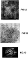
- the figures 1A and 1B represent photographs under observation by TEM of crude CZTS colloid prepared in a water / acetonitrile mixture according to Example 1, by measurement with a STEM detector ( figure 1A ) and at higher MET magnification ( figure 1B ), the figure 1C being a diffraction spectrum photograph obtained by ED electron diffraction of the dried powder.
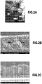
- FIGS. 2A, 2B and 2C represent photographs by SEM-type microscopy of CZTS nanoparticles in colloidal form ( figure 2A ), and after deposition in the form of a film deposited by spraying on a substrate ( figure 2B ), and after annealing at 525 ° C of said film ( figure 2C ).
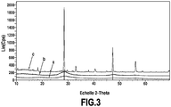
- the figure 3 is an X-ray diffraction spectrum measured on layers of nanoparticles of figures 2A (curve a), 2B (curve b) and 2C (curve c).
- the Cps values (“Strokes per second”) on the ordinate are in linear scale (“Lin”).
- the figures 4 A) to 4 D) represent photographs taken by electron microscopy, after crystallization annealing at 525 ° C, of the surface of a CZTS film according to Example 4 dispersed in a pure ethanol solvent and deposition by spraying at 75 ° C ( Fig. 4A ), PET solvent and spraying at 300 ° C ( Fig. 4B ), DMSO solvent and spraying at 300 ° C ( Fig. 4C ) and a water and spray solvent at 300 ° C ( Fig.4D ).
- a Cu-Zn-Sn-S nanoparticle colloid was made by reacting a mixture of metal salts of CuCl, ZnCl 2 , SnCl 4 : 5H 2 O in water / acetonitrile with an aqueous solution of NaSH, at room temperature and under an inert nitrogen atmosphere, depending on the overall reaction: 2CuCl + ZnCl 2 + SnCl 4 + 4NaSH ⁇ Cu 2 ZnSnS 4 + 4NaCl + 4HCl
- This reactive system is suitable in that the reaction by-products, for example NaCl or HCl, are soluble in water while the nanoparticles are solid, and dispersed as a colloid.
- reaction by-products for example NaCl or HCl
- the aqueous solution (0.12 M) of NaSH is prepared in a 50 ml bottle, by weighing 0.56 grams of hydrated NaSH powder (supplier Aldrich, product 16,152,7) and adding 50mL of deionized water beforehand. deoxygenated by bubbling for 30 minutes with nitrogen. This aqueous solution of NaSH sulfur precursor is then sealed with a stopper, and then stored.
- the colloidal synthesis reaction is carried out by pouring 10 ml of the solution (0.12 M) NaSH in 10 ml of solution of metal precursors (0.1 M) CZT. This synthesis, carried out at ambient pressure and temperature, is very rapid and gives rise to a colloidal solution CZTS, according to the overall reaction indicated above.
- This crude colloid was analyzed by Transmission Electron Microscopy.
- a model 2100 FEG 200kV from the company JEOL (Japan) is used, equipped with EDX (Energy-dispersive X-ray Spectroscopy), STEM BF (Scanning Transmission Electron Microscope Bright Field) and STEM DF (Surface Transmission Electron Microscope Dark Field) detectors.
- wide angle HAADF High Angular Annular Dark Field
- a sample holder made up of a carbon membrane on a nickel grid was soaked in undiluted colloid and then simply dried in ambient air before being introduced into the vacuum chamber of the TEM.
- the dried colloid forms aggregates of primary nanoparticles whose characteristic size is 2 to 5 nm and with a characteristic rounded shape of amorphous particles.
- the average elemental analysis carried out by EDX measurement over numerous zones indicates that these dried particles contain the majority elements Cu, Zn, Sn, S, and Cl as an impurity.
- Figure 1B At higher MET magnification ( Figure 1B ), ie by concentrating the beam of incident electrons, certain crystalline planes seem to be observable, attributable to a probable crystallization under beam, during the TEM observation.
- Electron diffraction analyzes show the presence of a diffuse diffraction ring, corresponding to atomic diffraction planes characterized by interatomic distances compatible with the known crystal structure of Cu 2 ZnSnS 4 kesterite (CZTS).
- CZTS Cu 2 ZnSnS 4 kesterite
- This crude colloid is then poured into a centrifuge tube and then centrifuged for 5 min at 6000 rev / min (Universal 16 centrifuge from the company Hettich Zentrifugen AG), ie an acceleration of 3700 G expressed with respect to gravity. This makes it possible to separate the solid and liquid parts.
- the transparent upper liquid part (the supernatant) is removed by pouring it into an acidic liquid waste bottle.
- the lower solid part is then rinsed by adding 20 ml of water. After introducing a magnetic bar covered with Teflon, this solution was placed on a magnetic plate and mixed by magnetic stirring at about 200 rpm for 5 minutes.
- This paste was then re-dispersed in a mixture of water / ethanol (5mL / 5mL), then mixed by magnetic stirring for 5 minutes at room temperature;
- the colloid obtained is then stable for a few days and can be used for deposition by spraying / atomization "spray".
- the particles in suspension in this rinsed colloid were analyzed by TEM microscopy ( Figure2A ) using the same procedure with carbon membrane on a nickel grid, as previously described for the TEM measurement of the crude colloid ( Figure1A ).
- Microscopy with a STEM DF detector of the Figure2A shows Primary nanoparticles of rounded shape, agglomerated and of similar size between 2 and 7 nm typically.
- EDX analysis indicates the majority presence of the elements Cu, Zn, Sn and S but the absence of chlorine element, which illustrates the effect of rinsing.
- the X-ray diffraction measurements were carried out in a Bruker AXS D8 series 2 diffractometer, using an X-ray source corresponding to the K ⁇ emission line of copper, in grazing mode (with an angle of incidence fixed at 1 ° ) and a detector moving on an arc of a circle to obtain a 2 hereby diffraction angle spectrum scanned from 10 ° to 70 ° with a step of 0.04 °.
- the curve has Figure 3 (lower spectrum) shows the X-ray diffraction spectrum of the wet paste of the Figure 2A .
- the particles composing the rinsed colloid then dried in ambient air are mainly amorphous or weakly crystallized, in agreement with the MET observations of the Figures 1A and 1B (crude colloid) or MET observations of the Figure 2A (rinsed and reconditioned or redispersed colloid).
- the solid nanoparticles of the crude colloid and of the rinsed and then redispersed colloid are both characterized by a nanometric size (2-7nm), composed of the elements Cu, Zn, Sn and S, of amorphous or even very weakly crystalline crystalline structure.
- the concentration of the CZTS colloid is defined as the number of molecules of the CZTS compound (Cu 2 ZnSnS 4 or in an equivalent manner the number of tin atoms) per unit of volume.
- the concentration of the crude colloid is 0.0125 M.
- the concentration of the CZTS colloid has been increased to 0.25 M, which is equivalent to about 100 mg / ml.
- an aqueous solution (6M) of NaSH is prepared, by weighing 2.24 g per 4 ml of solution.
- a solution of copper-zinc-tin (CZT) metal chlorides in acetonitrile is prepared by weighing 188 mg of CuCl, 166 mg of ZnCl 2 and 357 mg of hydrated SnCl 4 for 5 ml of solution.
- the synthesis is carried out by first pouring 11 ml of deionized and deoxygenated water into the solution of metal precursors, then in a second step the 4 ml of NaSH solution.
- the crude colloid of the CZTS compound thus produced is concentrated (0.25M) and, moreover, exhibits a high stability after the addition of water at the rinsing step indicated in Example 1 above.
- Example 3 Preparation of a film of CZTS crystallized on a glass substrate coated with molybdenum.
- composition of the crystallized film Cu 2 ZnSnS 4 and the composition of the amorphous film deposited by spray before annealing written in Cu-Zn-Sn-S form are distinguished below and in a conventional manner.
- Amorphous layers of Cu-Zn-Sn-S were deposited from nanoparticles in suspension, by spraying ("spray") on Mo / glass type substrates formed from soda-lime glass with a thickness of 1 mm covered with a layer of molybdenum of 700nm.
- a colloid was prepared in accordance with Example 1 above, then the colloid was re-dispersed in a mixture of water / ethanol (5mL / 5mL).
- the spraying step was carried out in a glove box (GP concept type T3 model in stainless steel, Jacomex SAS company, France) filled with nitrogen and equipped with a purification unit ( ⁇ 1ppm O 2 , ⁇ 10ppm H 2 O) and an airlock for entering / leaving samples.
- the amorphous Cu-Zn-Sn-S films were deposited on Mo / glass substrates (2.5cm x 2.5cm) brought to a temperature of 250 ° C using a heating plate (model 18x18cm ceramic standard, reference 444-0617 from VWR International SAS, France) with closed-loop modified thermal regulation on a type K thermocouple placed under the substrate.
- An XY Cartesian robot was used (of the Hyundai type, FXYx 550x550 with RCX222 controller, distributed in France by the company New-Mat France to sweep a surface of more than 16 cm 2 by the spray nozzle used (spray bottle on a test tube in borosilicate glass from Glasskeller Basel AG).
- the morphology of the amorphous Cu-Zn-Sn-S layers thus deposited was determined by SEM Scanning Electron Microscopy (Hitachi Ltd., model S-4700 equipped with EDX analyzer and data processing by NORAN software).
- the figure 2B is a section view of a Cu-Zn-Sn-S film spray deposited at 240 ° C. In this image we can see the glass substrate covered with a 700 nm layer of polycrystalline molybdenum with columnar structure, and the Cu-Zn-Sn-S film. It can be seen that this film is porous and composed of fine particles agglomerated together and separated by a vacuum.
- the annealing step serving for the densification and crystallization of the layer to form large crystalline grains was carried out in a nitrogen glove box (reference GT concept, from the company Jacomex SAS, France).
- the film deposited by spraying was then placed on a heating plate (titanium plate model with Detlef control box, company Harry Gesttechnik, GmbH) and heated under nitrogen gradually to an annealing temperature of 525 ° C maintained for 1 hour. , then cooled for 1 hour.
- the Figure 2C shows a sectional view of the film obtained after annealing: above the polycrystalline molybdenum layer, a polycrystalline film with a thickness of 1.8 ⁇ 0.2 ⁇ m reflects the densification of the film which is accompanied by crystallization with formation of the desired large grains (from 1 to 2 ⁇ m) that is to say close to the thickness of the film.
- the surface condition of the above film was analyzed and its roughness Sa was measured according to the ISO 25178 standard.
- the average roughness Sa is defined as the arithmetic mean of the absolute values of the ordinates of the roughness profile. The following values were obtained for a film with a thickness of 1.8 ⁇ m: 313 nm for a surface of 50 ⁇ 50 ⁇ m 2 , 247 nm for a surface of 20 ⁇ 20 ⁇ m 2 .
- Example 4 Preparation of a film of CZTS crystallized on a glass substrate coated with molybdenum from a CZTS ink formulated in pure dispersion solvents.
- a CZTS colloid was prepared in accordance with Example 1, except that the paste rinsed with water and then centrifuged was then mixed in dispersion solvents other than the water-ethanol mixture 50-50. of Example 3.
- four were selected for the present example in particular for their vapor pressures at 20 ° C low for TEP (Tri-Ethyl-Phosphate) (40 Pa) or DMSO (80 Pa ) or high for water (2330 Pa) and ethanol (5850 Pa) The concentration was adjusted to 10 g / L.
- the CZTS / Mo / glass samples obtained were then subjected to a crystallization heat treatment at 525 ° C. under nitrogen. The surface images of the samples obtained are shown on the Fig. 4A to 4D .
- This CZTS film is formed of crystallized CZTS grains as indicated by the X-ray diffraction spectra (not shown).
- A) ethanol B) Tri-Ethyl-Phosphate (TEP) or C) Di-Methyl-Sulf-Oxide (DMSO)
- TEP Tri-Ethyl-Phosphate
- DMSO Di-Methyl-Sulf-Oxide
- the present example shows that water is the preferred pure dispersion solvent.
- the dispersion solvent is preferably a water-ethanol mixture, which is an abundant solvent, easy to use and non-toxic and which makes it possible to produce, after deposition by spraying (spray) followed by thermal crystallization treatment, of Coarse-grained crystalline CZTS layers, continuous and dense (no cracks or holes) and adherent to the molybdenum substrate.
- Example 5 Preparation of a colloid of Sb 2 S 3 .
- a sulfur precursor solution is first prepared by mixing 18 ml of acetonitrile and 2 ml of water at room temperature, then by pouring 18 mg of NaSH powder (0.321 mmol) therein, which dissolves spontaneously. As NaSH is not or only slightly soluble in acetonitrile, dissolution takes place in the aqueous part of the water / acetonitrile mixture.
- a solution of antimony metal precursor with a concentration of 10.7 mol / liter is then prepared by dissolving 4 mg (0.214 mmol) of SbCl 3 powder (Aldrich) in a solution of 20 ml of pure acetonitrile. No hydrolysis of the SbCl 3 salt is observed during this dissolution.
- the MET + EDX elemental analysis shows a predominantly Sb 2 S 3 composition as well as the presence of chlorinated impurities (of the order of 1 atomic%).
- No crystalline phase is identifiable by electron diffraction under a TEM electron beam, which indicates that the solid particles of the colloid consist of amorphous Sb 2 S 3 antimony sulfide.
- a 0.05M metallic solution of tin is prepared in a 50mL glass bottle, into which 348 mg of tin precursor powder (anhydrous SnCl 2 , Fluka 96529) and then 36 ml of acetonitrile solvent are first poured. . Dissolution is facilitated at room temperature by ultrasonication for a few minutes.
- a 0.2M aqueous sulfur solution is prepared by weighing 1.12 g of NaSH powder, then by adding 100 ml of pure deionized and deoxygenated water to achieve their spontaneous dissolution.
- the colloidal synthesis is then carried out by mixing the two solutions at room temperature, for example by pouring 9 ml of the 0.2M sulfur solution into 36 ml of 0.05M metallic tin solution.
- This colloid is stable under ambient conditions for several days. The TEM observation of this colloid thus produced and without other treatment (without rinsing, centrifugation, redispersion, etc.) is presented below.
- the MET - EDX elemental analysis indicates that the composition is mainly tin sulphide, with the presence of chlorine impurity, which is a residual impurity from the reaction according to the following composition (MET EDX): Sn S Cl VS NOT O at.% 45.2 52.3 2.5 0.0 0.0 0.0 100
- the primary particles formed are relatively small, with a characteristic size of the order of 3 to 5 nm.
- This colloid can then be used to be rinsed and then reformulated in the form of a paste or an ink which can be used for depositing thin layers.
- Example 7 Photovoltaic device of the thin film type produced with a layer of CZTS annealed in a nitrogen atmosphere.
- a thin layer of CZTS was prepared on a molybdenum-coated glass substrate, annealed under an N 2 atmosphere, as in Example 3.
- a buffer layer of CdS of approximately 50 nm was deposited by chemical bath deposition according to the usual procedure of the state of the art (see for example G. Hodes, Chemical Solution Deposition Of Semiconductor Films, ISBN 08247-0851-2, M. Dekker Inc .), by quenching in a mixture maintained at 60 ° C of deionized water, ammonia (NH 3 , 4M), cadmium nitrate (Cd (NO 3 ) 2 , 4mM) and thiourea (SC (SC ( NH 2 ) 2 , 0.2M). After 10 minutes, the samples were rinsed in deionized water and then dried under a stream of nitrogen.
- the substrate was divided into 16 electrically isolated cells, each of 0.5 cm x 0.5 cm square dimensions.
- a front face contact was made by a small 0.5 mm silver dot deposited by drying a lacquer charged with silver, on the ITO conductive layer.
- the rear contact was taken directly on the Molybdenum, at the edge of the substrate.
- the photovoltaic efficiency (or photovoltaic efficiency) was calculated from the current-voltage electrical characteristics of the photovoltaic diode measured under light irradiation.
- This photovoltaic efficiency was measured with an electrical test bench and which uses a solar simulator delivering an irradiation of 1000 W / m 2 corresponding to the AM1.5G standard.
- the measurement bench was calibrated according to the standard procedure on the basis of the known photocurrent of reference cells, as supplied by various recognized official institutes.
Landscapes
- Chemical & Material Sciences (AREA)
- Organic Chemistry (AREA)
- Dispersion Chemistry (AREA)
- Chemical Kinetics & Catalysis (AREA)
- Engineering & Computer Science (AREA)
- Nanotechnology (AREA)
- Inorganic Chemistry (AREA)
- Crystallography & Structural Chemistry (AREA)
- General Physics & Mathematics (AREA)
- Condensed Matter Physics & Semiconductors (AREA)
- Physics & Mathematics (AREA)
- Manufacturing & Machinery (AREA)
- Composite Materials (AREA)
- Materials Engineering (AREA)
- Photovoltaic Devices (AREA)
- Life Sciences & Earth Sciences (AREA)
- Sustainable Development (AREA)
- Sustainable Energy (AREA)
- Colloid Chemistry (AREA)
- Liquid Deposition Of Substances Of Which Semiconductor Devices Are Composed (AREA)
Applications Claiming Priority (2)
| Application Number | Priority Date | Filing Date | Title |
|---|---|---|---|
| FR1257242A FR2993792B1 (fr) | 2012-07-26 | 2012-07-26 | Film de chalcogenure(s) metallique(s) cristallise(s) a gros grains, solution colloidale de particules amorphes et procedes de preparation. |
| PCT/FR2013/051597 WO2014016489A2 (fr) | 2012-07-26 | 2013-07-04 | Film de chalcogenure(s) metallique(s) cristallise(s) a gros grains, solution colloïdale de particules amorphes et procedes de preparation |
Publications (2)
| Publication Number | Publication Date |
|---|---|
| EP2877277A2 EP2877277A2 (fr) | 2015-06-03 |
| EP2877277B1 true EP2877277B1 (fr) | 2020-10-14 |
Family
ID=47501354
Family Applications (1)
| Application Number | Title | Priority Date | Filing Date |
|---|---|---|---|
| EP13745450.0A Not-in-force EP2877277B1 (fr) | 2012-07-26 | 2013-07-04 | Procédé de preparation de solution colloïdale de particules amorphes |
Country Status (5)
| Country | Link |
|---|---|
| US (3) | US9731262B2 (enExample) |
| EP (1) | EP2877277B1 (enExample) |
| JP (2) | JP6312668B2 (enExample) |
| FR (1) | FR2993792B1 (enExample) |
| WO (1) | WO2014016489A2 (enExample) |
Families Citing this family (17)
| Publication number | Priority date | Publication date | Assignee | Title |
|---|---|---|---|---|
| CN104028285A (zh) * | 2014-05-17 | 2014-09-10 | 北京工业大学 | Cu2ZnSnS4/La2Ti2O7异质结光催化复合材料的制备方法 |
| FR3022074B1 (fr) | 2014-06-05 | 2018-02-16 | Imra Europe Sas | Procede de preparation de couche mince d'absorbeur a base de sulfure(s) et seleniures(s) de cuivre, zinc et etain, couche mince recuite et dispositif photovoltaique obtenus. |
| US10888836B2 (en) * | 2014-07-25 | 2021-01-12 | Chemical and Metal Technologies LLC | Extraction of target materials using CZTS sorbent |
| US10730012B2 (en) * | 2014-07-25 | 2020-08-04 | Chemical and Metal Technologies LLC | Extraction of target materials using CZTS sorbent |
| US10283357B2 (en) * | 2014-12-01 | 2019-05-07 | The University Of Chicago | Compositionally matched molecular solders for semiconductors |
| US9825214B1 (en) * | 2016-06-22 | 2017-11-21 | Mainstream Engineering Corporation | Films and the like produced from particles by processing with electron beams, and a method for production thereof |
| US11167262B2 (en) * | 2017-09-29 | 2021-11-09 | Korea Institute Of Science And Technology | Amorphous nanostructure composed of inorganic polymer and method for manufacturing the same |
| WO2019066466A1 (ko) * | 2017-09-29 | 2019-04-04 | 한국과학기술연구원 | 무기 고분자로 이루어진 비정질 나노구조체 및 그 제조방법 |
| KR102432093B1 (ko) * | 2017-10-20 | 2022-08-16 | 한국과학기술연구원 | 무기 고분자로 이루어진 비정질 나노구조체 및 그 제조방법 |
| KR102458627B1 (ko) * | 2018-08-21 | 2022-10-25 | 한국과학기술연구원 | 비정질 나노구조체를 이용하여 제조된 프랙탈 형상의 합금 나노구조체 및 그 제조방법 |
| KR102407233B1 (ko) | 2018-08-21 | 2022-06-10 | 한국과학기술연구원 | 지지체의 나노 사이즈 기공 내에 나노입자가 고르게 분산된 복합체 및 이의 제조방법 |
| CN111474142B (zh) * | 2020-05-21 | 2021-08-03 | 中南大学 | 一种利用近红外1550nm激光器检测微塑料浓度的方法 |
| CN113321555A (zh) * | 2021-07-05 | 2021-08-31 | 多农多收技术研究(江苏)有限公司 | 一种可以有效阻止粮食作物对土壤中镉吸收的药剂及方法 |
| CN115108581B (zh) * | 2022-07-05 | 2024-03-15 | 许昌学院 | 一种常温制备铜锌锡硫纳米晶的化学方法 |
| CN115231608B (zh) * | 2022-07-06 | 2024-03-15 | 许昌学院 | 一种常温制备多元硫化物纳米晶的化学方法 |
| KR102671502B1 (ko) * | 2022-11-28 | 2024-05-30 | 전남대학교산학협력단 | 이중 버퍼층을 구비하는 박막 태양전지 및 이의 제조방법 |
| WO2024242138A1 (ja) * | 2023-05-25 | 2024-11-28 | カルコジェニック株式会社 | SnS分散液及びその製造方法 |
Citations (5)
| Publication number | Priority date | Publication date | Assignee | Title |
|---|---|---|---|---|
| WO1999037832A1 (en) * | 1998-01-27 | 1999-07-29 | Midwest Research Institute | Solution synthesis of mixed-metal chalcogenide nanoparticles and spray deposition of precursor films |
| WO2010124212A2 (en) * | 2009-04-23 | 2010-10-28 | The University Of Chicago | Materials and methods for the preparation of nanocomposites |
| WO2011066205A1 (en) * | 2009-11-25 | 2011-06-03 | E. I. Du Pont De Nemours And Company | Aqueous process for producing crystalline copper chalcogenide nanoparticles, the nanoparticles so-produced, and inks and coated substrates incorporating the nanoparticles |
| US20120070936A1 (en) * | 2010-09-20 | 2012-03-22 | International Business Machines Corporation | Annealing thin films |
| WO2014118444A1 (fr) * | 2013-01-29 | 2014-08-07 | Imra Europe Sas | Procédé de préparation de couche mince d'absorbeur à base de sulfure(s) de cuivre, zinc et étain, couche mince recuite et dispositif photovoltaïque obtenu |
Family Cites Families (13)
| Publication number | Priority date | Publication date | Assignee | Title |
|---|---|---|---|---|
| US4645619A (en) * | 1985-05-28 | 1987-02-24 | Xerox Corporation | Process for the preparation of colloidal dispersions of chalcogens and chalcogenide alloys |
| JP2005032475A (ja) | 2003-07-08 | 2005-02-03 | Sharp Corp | 有機色素を光増感剤とする半導体薄膜電極、それを用いた色素増感型光電変換素子および光電気化学太陽電池 |
| JP2007119535A (ja) * | 2005-10-25 | 2007-05-17 | Matsushita Electric Works Ltd | 光機能ナノ材料、その作製方法、発光ダイオード及び太陽電池 |
| US20080314738A1 (en) * | 2007-06-19 | 2008-12-25 | International Business Machines Corporation | Electrolytic Device Based on a Solution-Processed Electrolyte |
| JP5697449B2 (ja) | 2008-09-04 | 2015-04-08 | 株式会社カネカ | 透明電極付き基板および透明電極付き基板の製造方法 |
| WO2010048581A2 (en) * | 2008-10-24 | 2010-04-29 | Life Technologies Corporation | Stable nanoparticles and methods of making and using such particles |
| JP2010140812A (ja) * | 2008-12-12 | 2010-06-24 | Sekisui Chem Co Ltd | 機能素子及びその製造方法並びに色素増感太陽電池 |
| US7972899B2 (en) | 2009-07-30 | 2011-07-05 | Sisom Thin Films Llc | Method for fabricating copper-containing ternary and quaternary chalcogenide thin films |
| EP2504854A2 (en) * | 2009-11-25 | 2012-10-03 | E.I. Du Pont De Nemours And Company | CZTS/Se PRECURSOR INKS AND METHODS FOR PREPARING CZTS/Se THIN FILMS AND CZTS/Se-BASED PHOTOVOLTAIC CELLS |
| JP5454214B2 (ja) | 2010-02-22 | 2014-03-26 | Tdk株式会社 | 化合物半導体バッファ層の製造方法及び化合物半導体薄膜太陽電池の製造方法 |
| US9117964B2 (en) | 2010-06-29 | 2015-08-25 | Merck Patent Gmbh | Preparation of semiconductor films |
| US20130037110A1 (en) * | 2011-08-10 | 2013-02-14 | International Business Machines Corporation | Particle-Based Precursor Formation Method and Photovoltaic Device Thereof |
| TWI460869B (zh) * | 2011-12-30 | 2014-11-11 | Ind Tech Res Inst | 太陽能電池光吸收層之製法 |
-
2012
- 2012-07-26 FR FR1257242A patent/FR2993792B1/fr not_active Expired - Fee Related
-
2013
- 2013-07-04 US US14/413,316 patent/US9731262B2/en not_active Expired - Fee Related
- 2013-07-04 JP JP2015523587A patent/JP6312668B2/ja active Active
- 2013-07-04 WO PCT/FR2013/051597 patent/WO2014016489A2/fr not_active Ceased
- 2013-07-04 EP EP13745450.0A patent/EP2877277B1/fr not_active Not-in-force
-
2017
- 2017-07-21 US US15/655,952 patent/US10632441B2/en not_active Expired - Fee Related
-
2018
- 2018-03-20 JP JP2018052441A patent/JP6629374B2/ja not_active Expired - Fee Related
-
2020
- 2020-03-17 US US16/820,984 patent/US20200215509A1/en not_active Abandoned
Patent Citations (5)
| Publication number | Priority date | Publication date | Assignee | Title |
|---|---|---|---|---|
| WO1999037832A1 (en) * | 1998-01-27 | 1999-07-29 | Midwest Research Institute | Solution synthesis of mixed-metal chalcogenide nanoparticles and spray deposition of precursor films |
| WO2010124212A2 (en) * | 2009-04-23 | 2010-10-28 | The University Of Chicago | Materials and methods for the preparation of nanocomposites |
| WO2011066205A1 (en) * | 2009-11-25 | 2011-06-03 | E. I. Du Pont De Nemours And Company | Aqueous process for producing crystalline copper chalcogenide nanoparticles, the nanoparticles so-produced, and inks and coated substrates incorporating the nanoparticles |
| US20120070936A1 (en) * | 2010-09-20 | 2012-03-22 | International Business Machines Corporation | Annealing thin films |
| WO2014118444A1 (fr) * | 2013-01-29 | 2014-08-07 | Imra Europe Sas | Procédé de préparation de couche mince d'absorbeur à base de sulfure(s) de cuivre, zinc et étain, couche mince recuite et dispositif photovoltaïque obtenu |
Also Published As
| Publication number | Publication date |
|---|---|
| US20170320037A1 (en) | 2017-11-09 |
| FR2993792B1 (fr) | 2017-09-15 |
| JP2018113471A (ja) | 2018-07-19 |
| US9731262B2 (en) | 2017-08-15 |
| EP2877277A2 (fr) | 2015-06-03 |
| JP2015532611A (ja) | 2015-11-12 |
| US20200215509A1 (en) | 2020-07-09 |
| WO2014016489A2 (fr) | 2014-01-30 |
| FR2993792A1 (fr) | 2014-01-31 |
| WO2014016489A3 (fr) | 2014-09-12 |
| JP6312668B2 (ja) | 2018-04-18 |
| US10632441B2 (en) | 2020-04-28 |
| US20150194548A1 (en) | 2015-07-09 |
| JP6629374B2 (ja) | 2020-01-15 |
Similar Documents
| Publication | Publication Date | Title |
|---|---|---|
| EP2877277B1 (fr) | Procédé de preparation de solution colloïdale de particules amorphes | |
| Ramasamy et al. | Routes to copper zinc tin sulfide Cu 2 ZnSnS 4 a potential material for solar cells | |
| CA2706380C (en) | Preparation of nanoparticle material | |
| US20130316519A1 (en) | Techniques for Forming a Chalcogenide Thin Film Using Additive to a Liquid-Based Chalcogenide Precursor | |
| US20130037111A1 (en) | Process for Preparation of Elemental Chalcogen Solutions and Method of Employing Said Solutions in Preparation of Kesterite Films | |
| EP2951855B1 (fr) | Procédé de préparation de couche mince d'absorbeur à base de sulfure(s) de cuivre, zinc et étain, couche mince recuite et dispositif photovoltaïque obtenu | |
| EP2769405A1 (fr) | Procede de croissance en epaisseur de nanofeuillets colloïdaux et materiaux composes desdits nanofeuillets | |
| CN102361830A (zh) | 含CuInS2纳米颗粒的前体层的硒化 | |
| EP3114704B1 (fr) | Procédé de préparation de couche mince d'absorbeur a base de sulfure(s) et séléniures(s) de cuivre, zinc et étain, couche mince recuite et dispositif photovoltaïque obtenus | |
| FR2949773A1 (fr) | Materiau solide a l'etat divise, procede de fabrication d'un tel materiau et utilisation d'un tel materiau dans une cellule photovoltaique. | |
| JPWO2013047461A1 (ja) | 化合物半導体薄膜形成用インクおよびその製造方法 | |
| EP3423409B1 (fr) | Procede de preparation de nanofils de silicium et/ou de germanium | |
| Dong et al. | Silver sulfide thin film solar cells: materials, fabrication methods, devices, and challenges | |
| Chalapathi et al. | Synthesis of AgBiS2 films by sulfurizing Bi/Ag stacks for thin film photovoltaics | |
| EP3126292A1 (fr) | Oxydes et sulfures mixtes de bismuth et cuivre pour application photovoltaïque | |
| TWI595680B (zh) | 用於製備二硒化/二硫化銅銦鎵(cigs)奈米粒子之方法、由該方法製備之cigs奈米粒子及基於其之光伏打裝置 | |
| TWI570949B (zh) | 化合物半導體薄膜之製作方法及具備其化合物半導體薄膜之太陽能電池 | |
| CA3160175A1 (fr) | Encre a base de nanoparticules d'argent | |
| Saleh et al. | Preparation CuInSe | |
| FR2995452A1 (fr) | Ensemble pour cellule photovoltaique, procede de fabrication d'un tel ensemble et cellule photovoltaique le contenant |
Legal Events
| Date | Code | Title | Description |
|---|---|---|---|
| PUAI | Public reference made under article 153(3) epc to a published international application that has entered the european phase |
Free format text: ORIGINAL CODE: 0009012 |
|
| 17P | Request for examination filed |
Effective date: 20141210 |
|
| AK | Designated contracting states |
Kind code of ref document: A2 Designated state(s): AL AT BE BG CH CY CZ DE DK EE ES FI FR GB GR HR HU IE IS IT LI LT LU LV MC MK MT NL NO PL PT RO RS SE SI SK SM TR |
|
| AX | Request for extension of the european patent |
Extension state: BA ME |
|
| RIN1 | Information on inventor provided before grant (corrected) |
Inventor name: BOURDAIS, STEPHANE Inventor name: CUCCARO, YAN Inventor name: CHONE, CHRISTOPHE |
|
| DAX | Request for extension of the european patent (deleted) | ||
| STAA | Information on the status of an ep patent application or granted ep patent |
Free format text: STATUS: EXAMINATION IS IN PROGRESS |
|
| 17Q | First examination report despatched |
Effective date: 20171124 |
|
| GRAP | Despatch of communication of intention to grant a patent |
Free format text: ORIGINAL CODE: EPIDOSNIGR1 |
|
| STAA | Information on the status of an ep patent application or granted ep patent |
Free format text: STATUS: GRANT OF PATENT IS INTENDED |
|
| INTG | Intention to grant announced |
Effective date: 20200519 |
|
| GRAS | Grant fee paid |
Free format text: ORIGINAL CODE: EPIDOSNIGR3 |
|
| GRAA | (expected) grant |
Free format text: ORIGINAL CODE: 0009210 |
|
| STAA | Information on the status of an ep patent application or granted ep patent |
Free format text: STATUS: THE PATENT HAS BEEN GRANTED |
|
| AK | Designated contracting states |
Kind code of ref document: B1 Designated state(s): AL AT BE BG CH CY CZ DE DK EE ES FI FR GB GR HR HU IE IS IT LI LT LU LV MC MK MT NL NO PL PT RO RS SE SI SK SM TR |
|
| REG | Reference to a national code |
Ref country code: GB Ref legal event code: FG4D Free format text: NOT ENGLISH |
|
| REG | Reference to a national code |
Ref country code: AT Ref legal event code: REF Ref document number: 1323045 Country of ref document: AT Kind code of ref document: T Effective date: 20201015 Ref country code: CH Ref legal event code: EP |
|
| REG | Reference to a national code |
Ref country code: DE Ref legal event code: R096 Ref document number: 602013073266 Country of ref document: DE |
|
| REG | Reference to a national code |
Ref country code: IE Ref legal event code: FG4D Free format text: LANGUAGE OF EP DOCUMENT: FRENCH |
|
| REG | Reference to a national code |
Ref country code: AT Ref legal event code: MK05 Ref document number: 1323045 Country of ref document: AT Kind code of ref document: T Effective date: 20201014 |
|
| REG | Reference to a national code |
Ref country code: NL Ref legal event code: MP Effective date: 20201014 |
|
| PG25 | Lapsed in a contracting state [announced via postgrant information from national office to epo] |
Ref country code: PT Free format text: LAPSE BECAUSE OF FAILURE TO SUBMIT A TRANSLATION OF THE DESCRIPTION OR TO PAY THE FEE WITHIN THE PRESCRIBED TIME-LIMIT Effective date: 20210215 Ref country code: NL Free format text: LAPSE BECAUSE OF FAILURE TO SUBMIT A TRANSLATION OF THE DESCRIPTION OR TO PAY THE FEE WITHIN THE PRESCRIBED TIME-LIMIT Effective date: 20201014 Ref country code: NO Free format text: LAPSE BECAUSE OF FAILURE TO SUBMIT A TRANSLATION OF THE DESCRIPTION OR TO PAY THE FEE WITHIN THE PRESCRIBED TIME-LIMIT Effective date: 20210114 Ref country code: FI Free format text: LAPSE BECAUSE OF FAILURE TO SUBMIT A TRANSLATION OF THE DESCRIPTION OR TO PAY THE FEE WITHIN THE PRESCRIBED TIME-LIMIT Effective date: 20201014 Ref country code: RS Free format text: LAPSE BECAUSE OF FAILURE TO SUBMIT A TRANSLATION OF THE DESCRIPTION OR TO PAY THE FEE WITHIN THE PRESCRIBED TIME-LIMIT Effective date: 20201014 Ref country code: GR Free format text: LAPSE BECAUSE OF FAILURE TO SUBMIT A TRANSLATION OF THE DESCRIPTION OR TO PAY THE FEE WITHIN THE PRESCRIBED TIME-LIMIT Effective date: 20210115 |
|
| REG | Reference to a national code |
Ref country code: LT Ref legal event code: MG4D |
|
| PG25 | Lapsed in a contracting state [announced via postgrant information from national office to epo] |
Ref country code: PL Free format text: LAPSE BECAUSE OF FAILURE TO SUBMIT A TRANSLATION OF THE DESCRIPTION OR TO PAY THE FEE WITHIN THE PRESCRIBED TIME-LIMIT Effective date: 20201014 Ref country code: IS Free format text: LAPSE BECAUSE OF FAILURE TO SUBMIT A TRANSLATION OF THE DESCRIPTION OR TO PAY THE FEE WITHIN THE PRESCRIBED TIME-LIMIT Effective date: 20210214 Ref country code: LV Free format text: LAPSE BECAUSE OF FAILURE TO SUBMIT A TRANSLATION OF THE DESCRIPTION OR TO PAY THE FEE WITHIN THE PRESCRIBED TIME-LIMIT Effective date: 20201014 Ref country code: SE Free format text: LAPSE BECAUSE OF FAILURE TO SUBMIT A TRANSLATION OF THE DESCRIPTION OR TO PAY THE FEE WITHIN THE PRESCRIBED TIME-LIMIT Effective date: 20201014 Ref country code: AT Free format text: LAPSE BECAUSE OF FAILURE TO SUBMIT A TRANSLATION OF THE DESCRIPTION OR TO PAY THE FEE WITHIN THE PRESCRIBED TIME-LIMIT Effective date: 20201014 Ref country code: ES Free format text: LAPSE BECAUSE OF FAILURE TO SUBMIT A TRANSLATION OF THE DESCRIPTION OR TO PAY THE FEE WITHIN THE PRESCRIBED TIME-LIMIT Effective date: 20201014 Ref country code: BG Free format text: LAPSE BECAUSE OF FAILURE TO SUBMIT A TRANSLATION OF THE DESCRIPTION OR TO PAY THE FEE WITHIN THE PRESCRIBED TIME-LIMIT Effective date: 20210114 |
|
| PG25 | Lapsed in a contracting state [announced via postgrant information from national office to epo] |
Ref country code: HR Free format text: LAPSE BECAUSE OF FAILURE TO SUBMIT A TRANSLATION OF THE DESCRIPTION OR TO PAY THE FEE WITHIN THE PRESCRIBED TIME-LIMIT Effective date: 20201014 |
|
| REG | Reference to a national code |
Ref country code: DE Ref legal event code: R097 Ref document number: 602013073266 Country of ref document: DE |
|
| PG25 | Lapsed in a contracting state [announced via postgrant information from national office to epo] |
Ref country code: LT Free format text: LAPSE BECAUSE OF FAILURE TO SUBMIT A TRANSLATION OF THE DESCRIPTION OR TO PAY THE FEE WITHIN THE PRESCRIBED TIME-LIMIT Effective date: 20201014 Ref country code: SK Free format text: LAPSE BECAUSE OF FAILURE TO SUBMIT A TRANSLATION OF THE DESCRIPTION OR TO PAY THE FEE WITHIN THE PRESCRIBED TIME-LIMIT Effective date: 20201014 Ref country code: RO Free format text: LAPSE BECAUSE OF FAILURE TO SUBMIT A TRANSLATION OF THE DESCRIPTION OR TO PAY THE FEE WITHIN THE PRESCRIBED TIME-LIMIT Effective date: 20201014 Ref country code: EE Free format text: LAPSE BECAUSE OF FAILURE TO SUBMIT A TRANSLATION OF THE DESCRIPTION OR TO PAY THE FEE WITHIN THE PRESCRIBED TIME-LIMIT Effective date: 20201014 Ref country code: CZ Free format text: LAPSE BECAUSE OF FAILURE TO SUBMIT A TRANSLATION OF THE DESCRIPTION OR TO PAY THE FEE WITHIN THE PRESCRIBED TIME-LIMIT Effective date: 20201014 Ref country code: SM Free format text: LAPSE BECAUSE OF FAILURE TO SUBMIT A TRANSLATION OF THE DESCRIPTION OR TO PAY THE FEE WITHIN THE PRESCRIBED TIME-LIMIT Effective date: 20201014 |
|
| PLBE | No opposition filed within time limit |
Free format text: ORIGINAL CODE: 0009261 |
|
| STAA | Information on the status of an ep patent application or granted ep patent |
Free format text: STATUS: NO OPPOSITION FILED WITHIN TIME LIMIT |
|
| PG25 | Lapsed in a contracting state [announced via postgrant information from national office to epo] |
Ref country code: DK Free format text: LAPSE BECAUSE OF FAILURE TO SUBMIT A TRANSLATION OF THE DESCRIPTION OR TO PAY THE FEE WITHIN THE PRESCRIBED TIME-LIMIT Effective date: 20201014 |
|
| 26N | No opposition filed |
Effective date: 20210715 |
|
| PG25 | Lapsed in a contracting state [announced via postgrant information from national office to epo] |
Ref country code: AL Free format text: LAPSE BECAUSE OF FAILURE TO SUBMIT A TRANSLATION OF THE DESCRIPTION OR TO PAY THE FEE WITHIN THE PRESCRIBED TIME-LIMIT Effective date: 20201014 Ref country code: IT Free format text: LAPSE BECAUSE OF FAILURE TO SUBMIT A TRANSLATION OF THE DESCRIPTION OR TO PAY THE FEE WITHIN THE PRESCRIBED TIME-LIMIT Effective date: 20201014 |
|
| PG25 | Lapsed in a contracting state [announced via postgrant information from national office to epo] |
Ref country code: SI Free format text: LAPSE BECAUSE OF FAILURE TO SUBMIT A TRANSLATION OF THE DESCRIPTION OR TO PAY THE FEE WITHIN THE PRESCRIBED TIME-LIMIT Effective date: 20201014 |
|
| REG | Reference to a national code |
Ref country code: DE Ref legal event code: R119 Ref document number: 602013073266 Country of ref document: DE |
|
| REG | Reference to a national code |
Ref country code: CH Ref legal event code: PL |
|
| GBPC | Gb: european patent ceased through non-payment of renewal fee |
Effective date: 20210704 |
|
| PG25 | Lapsed in a contracting state [announced via postgrant information from national office to epo] |
Ref country code: MC Free format text: LAPSE BECAUSE OF FAILURE TO SUBMIT A TRANSLATION OF THE DESCRIPTION OR TO PAY THE FEE WITHIN THE PRESCRIBED TIME-LIMIT Effective date: 20201014 |
|
| REG | Reference to a national code |
Ref country code: BE Ref legal event code: MM Effective date: 20210731 |
|
| PG25 | Lapsed in a contracting state [announced via postgrant information from national office to epo] |
Ref country code: LI Free format text: LAPSE BECAUSE OF NON-PAYMENT OF DUE FEES Effective date: 20210731 Ref country code: GB Free format text: LAPSE BECAUSE OF NON-PAYMENT OF DUE FEES Effective date: 20210704 Ref country code: DE Free format text: LAPSE BECAUSE OF NON-PAYMENT OF DUE FEES Effective date: 20220201 Ref country code: CH Free format text: LAPSE BECAUSE OF NON-PAYMENT OF DUE FEES Effective date: 20210731 |
|
| PG25 | Lapsed in a contracting state [announced via postgrant information from national office to epo] |
Ref country code: IS Free format text: LAPSE BECAUSE OF FAILURE TO SUBMIT A TRANSLATION OF THE DESCRIPTION OR TO PAY THE FEE WITHIN THE PRESCRIBED TIME-LIMIT Effective date: 20210214 Ref country code: LU Free format text: LAPSE BECAUSE OF NON-PAYMENT OF DUE FEES Effective date: 20210704 Ref country code: FR Free format text: LAPSE BECAUSE OF NON-PAYMENT OF DUE FEES Effective date: 20210731 |
|
| PG25 | Lapsed in a contracting state [announced via postgrant information from national office to epo] |
Ref country code: IE Free format text: LAPSE BECAUSE OF NON-PAYMENT OF DUE FEES Effective date: 20210704 Ref country code: BE Free format text: LAPSE BECAUSE OF NON-PAYMENT OF DUE FEES Effective date: 20210731 |
|
| PG25 | Lapsed in a contracting state [announced via postgrant information from national office to epo] |
Ref country code: HU Free format text: LAPSE BECAUSE OF FAILURE TO SUBMIT A TRANSLATION OF THE DESCRIPTION OR TO PAY THE FEE WITHIN THE PRESCRIBED TIME-LIMIT; INVALID AB INITIO Effective date: 20130704 |
|
| PG25 | Lapsed in a contracting state [announced via postgrant information from national office to epo] |
Ref country code: CY Free format text: LAPSE BECAUSE OF FAILURE TO SUBMIT A TRANSLATION OF THE DESCRIPTION OR TO PAY THE FEE WITHIN THE PRESCRIBED TIME-LIMIT Effective date: 20201014 |
|
| PG25 | Lapsed in a contracting state [announced via postgrant information from national office to epo] |
Ref country code: MK Free format text: LAPSE BECAUSE OF FAILURE TO SUBMIT A TRANSLATION OF THE DESCRIPTION OR TO PAY THE FEE WITHIN THE PRESCRIBED TIME-LIMIT Effective date: 20201014 |
|
| PG25 | Lapsed in a contracting state [announced via postgrant information from national office to epo] |
Ref country code: TR Free format text: LAPSE BECAUSE OF FAILURE TO SUBMIT A TRANSLATION OF THE DESCRIPTION OR TO PAY THE FEE WITHIN THE PRESCRIBED TIME-LIMIT Effective date: 20201014 |
|
| PG25 | Lapsed in a contracting state [announced via postgrant information from national office to epo] |
Ref country code: MT Free format text: LAPSE BECAUSE OF FAILURE TO SUBMIT A TRANSLATION OF THE DESCRIPTION OR TO PAY THE FEE WITHIN THE PRESCRIBED TIME-LIMIT Effective date: 20201014 |