EP2869549B1 - Camera module and electronic device - Google Patents
Camera module and electronic device Download PDFInfo
- Publication number
- EP2869549B1 EP2869549B1 EP13809413.1A EP13809413A EP2869549B1 EP 2869549 B1 EP2869549 B1 EP 2869549B1 EP 13809413 A EP13809413 A EP 13809413A EP 2869549 B1 EP2869549 B1 EP 2869549B1
- Authority
- EP
- European Patent Office
- Prior art keywords
- flexible substrate
- rigid substrate
- substrate
- camera module
- rigid
- Prior art date
- Legal status (The legal status is an assumption and is not a legal conclusion. Google has not performed a legal analysis and makes no representation as to the accuracy of the status listed.)
- Not-in-force
Links
Images








Classifications
-
- H—ELECTRICITY
- H04—ELECTRIC COMMUNICATION TECHNIQUE
- H04N—PICTORIAL COMMUNICATION, e.g. TELEVISION
- H04N23/00—Cameras or camera modules comprising electronic image sensors; Control thereof
- H04N23/50—Constructional details
- H04N23/54—Mounting of pick-up tubes, electronic image sensors, deviation or focusing coils
-
- H—ELECTRICITY
- H04—ELECTRIC COMMUNICATION TECHNIQUE
- H04N—PICTORIAL COMMUNICATION, e.g. TELEVISION
- H04N23/00—Cameras or camera modules comprising electronic image sensors; Control thereof
- H04N23/50—Constructional details
- H04N23/55—Optical parts specially adapted for electronic image sensors; Mounting thereof
-
- H—ELECTRICITY
- H04—ELECTRIC COMMUNICATION TECHNIQUE
- H04N—PICTORIAL COMMUNICATION, e.g. TELEVISION
- H04N23/00—Cameras or camera modules comprising electronic image sensors; Control thereof
- H04N23/57—Mechanical or electrical details of cameras or camera modules specially adapted for being embedded in other devices
-
- H—ELECTRICITY
- H10—SEMICONDUCTOR DEVICES; ELECTRIC SOLID-STATE DEVICES NOT OTHERWISE PROVIDED FOR
- H10F—INORGANIC SEMICONDUCTOR DEVICES SENSITIVE TO INFRARED RADIATION, LIGHT, ELECTROMAGNETIC RADIATION OF SHORTER WAVELENGTH OR CORPUSCULAR RADIATION
- H10F39/00—Integrated devices, or assemblies of multiple devices, comprising at least one element covered by group H10F30/00, e.g. radiation detectors comprising photodiode arrays
- H10F39/80—Constructional details of image sensors
- H10F39/804—Containers or encapsulations
-
- H—ELECTRICITY
- H10—SEMICONDUCTOR DEVICES; ELECTRIC SOLID-STATE DEVICES NOT OTHERWISE PROVIDED FOR
- H10F—INORGANIC SEMICONDUCTOR DEVICES SENSITIVE TO INFRARED RADIATION, LIGHT, ELECTROMAGNETIC RADIATION OF SHORTER WAVELENGTH OR CORPUSCULAR RADIATION
- H10F39/00—Integrated devices, or assemblies of multiple devices, comprising at least one element covered by group H10F30/00, e.g. radiation detectors comprising photodiode arrays
- H10F39/80—Constructional details of image sensors
- H10F39/806—Optical elements or arrangements associated with the image sensors
-
- H—ELECTRICITY
- H10—SEMICONDUCTOR DEVICES; ELECTRIC SOLID-STATE DEVICES NOT OTHERWISE PROVIDED FOR
- H10W—GENERIC PACKAGES, INTERCONNECTIONS, CONNECTORS OR OTHER CONSTRUCTIONAL DETAILS OF DEVICES COVERED BY CLASS H10
- H10W72/00—Interconnections or connectors in packages
- H10W72/50—Bond wires
-
- H—ELECTRICITY
- H10—SEMICONDUCTOR DEVICES; ELECTRIC SOLID-STATE DEVICES NOT OTHERWISE PROVIDED FOR
- H10W—GENERIC PACKAGES, INTERCONNECTIONS, CONNECTORS OR OTHER CONSTRUCTIONAL DETAILS OF DEVICES COVERED BY CLASS H10
- H10W72/00—Interconnections or connectors in packages
- H10W72/071—Connecting or disconnecting
- H10W72/075—Connecting or disconnecting of bond wires
-
- H—ELECTRICITY
- H10—SEMICONDUCTOR DEVICES; ELECTRIC SOLID-STATE DEVICES NOT OTHERWISE PROVIDED FOR
- H10W—GENERIC PACKAGES, INTERCONNECTIONS, CONNECTORS OR OTHER CONSTRUCTIONAL DETAILS OF DEVICES COVERED BY CLASS H10
- H10W72/00—Interconnections or connectors in packages
- H10W72/50—Bond wires
- H10W72/541—Dispositions of bond wires
- H10W72/5445—Dispositions of bond wires being orthogonal to a side surface of the chip, e.g. parallel arrangements
-
- H—ELECTRICITY
- H10—SEMICONDUCTOR DEVICES; ELECTRIC SOLID-STATE DEVICES NOT OTHERWISE PROVIDED FOR
- H10W—GENERIC PACKAGES, INTERCONNECTIONS, CONNECTORS OR OTHER CONSTRUCTIONAL DETAILS OF DEVICES COVERED BY CLASS H10
- H10W72/00—Interconnections or connectors in packages
- H10W72/90—Bond pads, in general
- H10W72/931—Shapes of bond pads
- H10W72/932—Plan-view shape, i.e. in top view
-
- H—ELECTRICITY
- H10—SEMICONDUCTOR DEVICES; ELECTRIC SOLID-STATE DEVICES NOT OTHERWISE PROVIDED FOR
- H10W—GENERIC PACKAGES, INTERCONNECTIONS, CONNECTORS OR OTHER CONSTRUCTIONAL DETAILS OF DEVICES COVERED BY CLASS H10
- H10W72/00—Interconnections or connectors in packages
- H10W72/90—Bond pads, in general
- H10W72/951—Materials of bond pads
-
- H—ELECTRICITY
- H10—SEMICONDUCTOR DEVICES; ELECTRIC SOLID-STATE DEVICES NOT OTHERWISE PROVIDED FOR
- H10W—GENERIC PACKAGES, INTERCONNECTIONS, CONNECTORS OR OTHER CONSTRUCTIONAL DETAILS OF DEVICES COVERED BY CLASS H10
- H10W72/00—Interconnections or connectors in packages
- H10W72/90—Bond pads, in general
- H10W72/951—Materials of bond pads
- H10W72/952—Materials of bond pads comprising metals or metalloids, e.g. PbSn, Ag or Cu
-
- H—ELECTRICITY
- H10—SEMICONDUCTOR DEVICES; ELECTRIC SOLID-STATE DEVICES NOT OTHERWISE PROVIDED FOR
- H10W—GENERIC PACKAGES, INTERCONNECTIONS, CONNECTORS OR OTHER CONSTRUCTIONAL DETAILS OF DEVICES COVERED BY CLASS H10
- H10W74/00—Encapsulations, e.g. protective coatings
-
- H—ELECTRICITY
- H10—SEMICONDUCTOR DEVICES; ELECTRIC SOLID-STATE DEVICES NOT OTHERWISE PROVIDED FOR
- H10W—GENERIC PACKAGES, INTERCONNECTIONS, CONNECTORS OR OTHER CONSTRUCTIONAL DETAILS OF DEVICES COVERED BY CLASS H10
- H10W90/00—Package configurations
- H10W90/701—Package configurations characterised by the relative positions of pads or connectors relative to package parts
- H10W90/751—Package configurations characterised by the relative positions of pads or connectors relative to package parts of bond wires
- H10W90/754—Package configurations characterised by the relative positions of pads or connectors relative to package parts of bond wires between a chip and a stacked insulating package substrate, interposer or RDL
Definitions
- the present technology relates to a camera module and an electronic device, and in particular, to a camera module in which a thin camera module can be realized at a low cost and an electronic device.
- FPC Flexible Printed Circuits
- ACF Anisotropic Conductive Film
- the thickness of the FPC and the thickness of the connecting portion are included in the height of the module such as a lens unit, whereby there is a problem that the thickness of the module increases.
- a rigid flexible substrate in which a rigid portion and a flexible portion are integrated, may also be used. In that case, there is no need to take into account a connection between the rigid substrate and the FPC.
- Patent Document 1 Japanese Patent Application Laid-Open No. 2009-033481
- a range of process conditions such as an ultrasonic wave, temperature setting, and the like becomes narrow when an image sensor is wire-bonded, and the like.
- US 2006/0091487 A1 relates to a manufacturing method of a solid state image sensing device and to such a solid state image sensing device to be used for a mobile communication device in which a wiring substrate protrudes from the bottom surface of a lens unit to thereby allow a flexible substrate to be attached on the upper side of the surface of wiring substrate carrying the lens unit.
- US 2011/0002685 A1 discloses a similar device wherein a base plate carries a circuit board on which a lens unit is mounted.
- the present technology is disclosed in view of such a situation, and aims to realize a thin camera module at a low cost.
- the invention provides a camera module in accordance with claim 1. Further aspects of the invention are set forth in the dependent claims, the drawings and the following description of embodiments.
- a thin camera module can be realized at a low cost.
- Fig. 1 is a perspective view illustrating an exemplary configuration of a conventional camera module.
- a camera module 10 illustrated in the figure is to be installed in an electronic device such as a mobile telephone or a smartphone.
- the camera module 10 in Fig. 1 is configured of a lens unit 11, a frame 12, a rigid substrate 13, and a flexible substrate 14.
- a flexible substrate is also referred to as FPC (Flexible Printed Circuits).
- the lens unit 11 is a unit which stores a lens of the camera, and the like. Light condensed through the lens in the lens unit 11 forms an image on a light receiving surface of an image sensor, described below, whereby an image is captured.
- the frame 12 is a standardized connecting component to be used for connection with the rigid substrate 13, for example, and is also used for improving shielding property, and the like. It should be noted that the frame 12 may not be provided. In that case, the lens unit 11 is directly attached to the rigid substrate 13.
- the rigid substrate 13 is a substrate on which an image sensor of the camera is disposed, for example.
- the flexible substrate 14 is a substrate on which wiring for inputting and outputting signals, input or output to/from the camera module 10, to/from another unit of an electronic device is printed, for example.
- the flexible substrate 14 is attached to the bottom surface (surface on the lower side in the figure) of the rigid substrate 13.
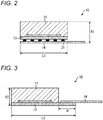
- Fig. 2 is a side view explaining an exemplary configuration of the conventional camera module 10. It should be noted that in the camera module 10 illustrated in Fig. 2 , the frame 12 in Fig. 1 is not provided and the lens unit 11 is directly attached to the rigid substrate 13.
- the flexible substrate 14 is attached to the bottom surface of the rigid substrate 13, which is the same as the case explained with reference to Fig. 1 . It should be note that in this example, solder balls 21 used for attaching the flexible substrate 14 and the rigid substrate 13 are illustrated.
- the thickness (height in the figure) of the camera module 10, configured as illustrated in Fig. 2 is represented as H1, and the height H1 includes the thickness of the flexible substrate 14 and the thickness of the solder ball 21.
- the length, in a horizontal direction in the figure, of the camera module 10 is represented as L1. It should be noted that in this example, the length in the horizontal direction of the camera module 10 does not include a portion where only the flexible substrate 14 exists.
- a range of process conditions such as an ultrasonic wave, temperature setting, and the like becomes narrow when an image sensor is wire-bonded.
- the rigid substrate 13 may be configured to protrude from the bottom surface of the lens unit 11 in order to reduce the thickness of the entire module to thereby allow the flexible substrate 14 to be attached on the surface (surface on the upper side in the figure) of the rigid substrate 13.
- the thickness of the camera module 10 is H2, which is less than H1. As such, it is possible to configure the camera module 10 to be thinner, compared with the case of Fig. 1 .
- the length of the entire camera module in the horizontal direction in the figure also extends.
- the length of the camera module 10 in the horizontal direction in the figure is L2 which is larger than L1.
- a mobile telephone, a smartphone, or the like must be designed while taking into account an increase in the length of the camera module 10 in the horizontal direction.
- the present technology configures a camera module as illustrated in Fig. 4 , for example.
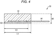
- Fig. 4 is a side view explaining an exemplary configuration of a camera module 50 to which the present technology is applied. It should be noted that in the camera module 50 illustrated in Fig. 4 , the frame described in Fig. 1 is not provided, and a lens unit 51 is directly attached to the rigid substrate 53.
- a left end portion, in the figure, of a flexible substrate 54 is interposed between the lens unit 51 and the rigid substrate 53.
- the camera module 50 to which the present technology is applied, is configured such that only an end portion on the left side, in the figure, of the flexible substrate 54 is attached to an end portion on the right side, in the figure, of the surface of the rigid substrate 53. Further, in the camera module 50 to which the present technology is applied, a groove for accommodating the left end portion of the flexible substrate 54 is provided on an end portion on the right side, in the figure, of the lens unit 51, the details of which will be described below.
- the thickness of the camera module 50 is H2. As such, it is possible to configure the camera module to be thinner, compared with the case of Fig. 1 .
- the length of the camera module 50 in the horizontal direction in the figure is L1. Accordingly, the length of the entire camera module in the horizontal direction in the figure does not extend, as in the configuration illustrated in Fig. 3 .
- the length of the flexible substrate 54 in the horizontal direction in the figure can be configured to be shorter.
- the flexible substrate 54 in Fig. 4 is configured to have a length shorter by a length L3 in the horizontal direction in the figure, compared with the case of the flexible substrate 14 in Fig. 1 , for example.
- the area of the flexible substrate can be reduced by the amount corresponding to the length L3, compared with the configuration of Fig. 1 .
- the area of an expensive flexible substrate is reduced, whereby the cost of the entire camera module can also be reduced.
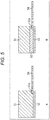
- Figs 5A and 5B are another side views explaining an exemplary configuration of the camera module 50 to which the present technology is applied.
- Fig. 5A is a diagram illustrating an exemplary configuration on the case where a frame is not provided in the camera module 50
- Fig. 5B is a diagram illustrating an exemplary configuration of the case where a frame is provided in the camera module 50.
- a left end portion, in the figure, of the flexible substrate 54 is interposed between the lens unit 51 and the rigid substrate 53.
- the camera module 50 to which the present technology is applied, is configured such that only an end portion on the left side, in the figure, of the flexible substrate 54 is attached to an end portion on the right side, in the figure, of the surface of the rigid substrate 53. Further, in the example of Fig. 5A , a groove 51a for accommodating the left end portion of the flexible substrate 54 is formed in an end portion on the right side, in the figure, of the lens unit 51.
- a frame 52 is provided between the lens unit 51 and the rigid substrate 53, and a left end portion, in the figure, of the flexible substrate 54 is interposed between the frame 52 and the rigid substrate 53. Further, in the example of Fig. 5B , a groove 52a for accommodating the left end portion of the flexible substrate 54 is formed in an end portion on the right side, in the figure, of the frame 52.
- the groove 51a or the groove 52a is not formed, for example, the right side in the figure of the lens unit 51 floats due to the thickness of the flexible substrate 54, whereby there is a possibility that the light condensed by the lens in the lens unit 51 does not form an image appropriately on the imaging surface of the image sensor on the rigid substrate 53.
- the parallel degree of the top surface (surface on the upper side in the figure) of the lens unit 51 and the imaging surface of the image sensor 61 becomes 1.5 degrees or smaller.
- the lens unit 51 or the frame 52 is attached to the rigid substrate 53 with an adhesive or the like, by adjusting the thickness of the adhesive, for example, it is possible to perform tilt adjustment so as to set the focus position of the lens in the lens unit 51 to be appropriate.
- the right side, in the figure, of the lens unit 51 floats due to the thickness of the flexible substrate 54.
- the adhesive must be injected in extra amounts for that portion, into a left-side portion in the figure.
- the attachment strength of the lens unit 51 or the frame 52 may be insufficient, or light transmitted through the adhesive may leak in the image sensor.
- the camera module may be configured without forming the groove 51a or the groove 52a.
- Fig. 6 is a plan view of the camera module 50 illustrated in Figs 5A and 5B , viewed from the upper direction of Figs 5A and 5B . It should be noted that in Fig. 6 , the lens unit 51 and the frame 52 are not illustrated for easy understanding.
- a rectangle image sensor 61 is disposed on the almost center of the rigid substrate 53.
- the front side of the sheet is the imaging surface of the image sensor 61.
- a portion on the left side, in the figure, of the flexible substrate 54 overlaps a portion on the right side, in the figure, of the rigid substrate 53. In the overlapped portion, the flexible substrate 54 and the rigid substrate 53 are attached, or electrically connected, to each other.
- the flexible substrate 54 is disposed on the rigid substrate 53 (on the light receiving side of the image sensor 61).
- Fig. 7 is another plan view of the camera module 50 illustrated in Figs 5A and 5B , viewed from the upper direction of Figs 5A and 5B .
- an illustration of the frame 52 is added, which is different from Fig. 6 .
- a portion on the left side, in the figure, of the flexible substrate 54 overlaps a portion on the right side, in the figure, of the frame 52, and the flexible substrate 54 is disposed under the frame 52. Further, the center of the frame 52 is formed as a cavity, whereby the imaging surface of the image sensor 61 is seen.
- Fig. 8 is a plan view illustrating a detailed exemplary configuration of the frame 52 of Fig. 7 .
- This figure is a diagram illustrating the frame 52 seen from the lower direction (rear side of the sheet) of Fig. 7 , in which the bottom surface of the frame 52 is illustrated.
- the groove 52a is formed on the right side, in the figure, of the frame 52.
- the center portion of the frame 52 is formed as a cavity, as described above.
- Fig. 9 is a cross-sectional view of the frame 52 taken along the alternate long and short dash line A-A' of Fig. 8 . As illustrated in the figure, the groove 52a is formed on the right side in the figure.
- Fig. 10 is a plan view illustrating another detailed exemplary configuration of the frame 52 of Fig. 7 .
- This figure is a diagram illustrating the frame 52 seen from the lower direction of Fig. 7 , in which the bottom surface of the frame 52 is illustrated.
- the groove 52a is formed on the right side, in the figure, of the frame 52.
- the center portion of the frame 52 is formed as a cavity, as described above.
- the groove 52a is formed across the rigid substrate 53 from the top to the bottom in the figure, which is different from the case of Fig. 8 .
- the groove 52a may be formed in this way.
- Fig. 11 is a cross-sectional view of the frame 52, taken along the alternate long and short dash line A-A' of Fig. 10 . As illustrated in the figure, the groove 52a is formed on the right side in the figure.
- the groove 52a is formed in the frame 52
- this also applies to the case where the groove 51a is formed in the lens unit 51.
- the groove 51a may be formed across the entire lens unit 51 from the top to the bottom as in the case of Fig. 10 , or the groove 51a may be formed in such a manner that the upper side and the lower side of the lens unit 51 are left, as in the case of Fig. 8 .
- a solder resist (SR) serving as an insulation film protecting the circuit pattern, for example is provided on the surface of the rigid substrate 53.
- the SR must be removed beforehand in a portion of the surface of the rigid substrate 53, in order to connect a connection terminal of the flexible substrate 54 and a connection terminal of the rigid substrate 53 with each other.
- Fig. 12 is a plan view of the camera module 50 illustrated in Figs 5A and 5B , viewed from the upper direction of Figs 5A and 5B . It should be noted that in Fig. 12 , the lens unit 51 and the frame 52 are not illustrated for easy understanding.
- the rectangle image sensor 61 is disposed on the almost center of the rigid substrate 53.
- a portion on the left side, in the figure, of the flexible substrate 54 overlaps a portion on the right side, in the figure, of the rigid substrate 53.
- the SR is removed and a connection terminal portion 53a is formed.
- connection terminal portion is formed in a portion on the left side in the figure.
- a connection terminal portion is provided on the rear face of the flexible substrate 54, it is not illustrated.
- connection terminal portion 53a of the rigid substrate 53 and the connection terminal portion, not illustrated, of the flexible substrate 54 are provided with connection terminals, respectively, and the connection terminal of the rigid substrate 53 of the rigid substrate 53 and the connection terminal of the flexible substrate 54 are attached, whereby the rigid substrate 53 and the flexible substrate 54 are connected electrically.
- Fig. 13 is a plan view illustrating the configuration of the flexible substrate 54 and the rigid substrate 53 illustrated in Fig. 12 , in detail.
- the image sensor 61 is illustrated in more detail.
- a portion on the left side, in the figure, of the flexible substrate 54 overlaps a portion on the right side, in the figure, of the rigid substrate 53.
- the overlapped portion is illustrated as an overlap width W.
- the overlap width W is represented as a distance from an end potion of one side (e.g., a side on the right side in Fig. 13 ) of a square rigid substrate, and in the band region of the overlap width W, the flexible substrate 54 and the rigid substrate 53 are attached to each other in an overlapped manner.
- the overlap width W is desirably 2.4 mm or less, for example.
- Figs. 14A to 14F are diagrams explaining an example of a manufacturing process of a camera module to which the present technology is applied.
- the rigid substrate 53 on which a component 62 is mounted, is prepared. It should be noted that as described with reference to Fig. 12 , the SR is removed in a portion on the right side, in the figure, of the rigid substrate 53, and the connection terminal portion 53a is formed.
- the flexible substrate 54 is attached to the rigid substrate 53.
- the rigid substrate 53 and the flexible substrate 54 are attached to each other in the overlap width W, and the connection terminal disposed in the connection terminal portion 53a and the connection terminal of the flexible substrate 54 are attached to thereby be connected electrically.
- solder an adhesive including solder, ACF, ACP, or the like is used.
- the image sensor 61 is die-bonded (DB) to the rigid substrate 53.
- wire-bonding (WB) is performed between the image sensor 61 and the rigid substrate 53.
- a wire 63 is wire-bonded.
- an adhesive is applied.
- an adhesive 64 is applied to both left and right sides of the rigid substrate 53.
- resin which attenuates light is used as the adhesive 64.
- black resin, resin containing filler, or the like is used as the adhesive 64.
- the frame 52 or the lens unit 51 is attached to rigid substrate 53.
- the frame 52 is attached to the rigid substrate 53
- the lens unit 51 is attached to the rigid substrate 53.
- the parallel degree of the top surface of the lens unit 51 and the imaging surface of the image sensor 61 is 1.5 degrees or less.
- the camera module to which the present technology is applied is manufactured through this manufacturing process.
- the flexible substrate 54 and the rigid substrate 53 are attached in the portion where a portion of the flexible substrate 54 overlaps a portion of the rigid substrate 53 (overlap width). As such, according to the usage conditions of the camera module, it may be desired to improve the break strength of the flexible substrate 54.
- Fig. 15 is a diagram explaining another configuration of the flexible substrate 54 in the camera module to which the present technology is applied. This figure is a diagram corresponding to Fig. 6 , and parts corresponding to those of Fig. 6 are denoted by the same reference signs.
- a reinforced portion 54a is provided to the flexible substrate 54.
- the reinforced portions 54a extending in a left direction in the figure, are provided to an end on the upper side and an end on the lower side, in the figure, of the flexible substrate 54. This means that in the flexible substrate 54, the reinforced portions 54a, extending in parallel with two sides of the square image sensor 61, are provided.
- reinforced portions 54a are provided at positions where they are not brought into contact with the image sensor 61, they do not affect the arrangement of the image sensor 61.
- the flexible substrate 54 By configuring the flexible substrate 54 as illustrated in Fig. 15 , it is possible to improve the break strength of the flexible substrate 54 according to the usage conditions of the camera module, for example.
- the flexible substrate 54 in the camera module to which the present technology is applied may be configured as illustrated in Fig. 16 .
- This figure is a diagram corresponding to Fig. 6 , and the parts corresponding to those of Fig. 6 are denoted by the same reference signs.
- a reinforced portion 54b is provided to the flexible substrate 54.
- the reinforced portions 54b extending in an up and down direction in the figure, are provided to an end portion on the upper side and an end portion on the lower side, in the figure, of the flexible substrate 54. This means that in the flexible substrate 54, the reinforced portions 54b, extending in parallel with one side of the square image sensor 61, are provided.
- reinforced portions 54b are provided at positions where they are not brought into contact with the image sensor 61, they do not affect the arrangement of the image sensor 61.
- the flexible substrate 54 By configuring the flexible substrate 54 as illustrated in Fig. 16 , it is possible to improve the break strength of the flexible substrate 54 according to the usage conditions of the camera module, for example.
- connection terminal of the rigid substrate 53 and the connection terminal of the flexible substrate 54 are attached to each other, whereby the image sensor 61 and the flexible substrate 54 are connected electrically.
- the rigid substrate 53 is required to be larger by the width for at least the overlap width and the wire bonding, compared with the image sensor 61.
- Fig. 17 is a side view explaining a necessary distance which is a distance from an end of the image sensor 61 to an end of the rigid substrate 53.
- a necessary distance is a distance corresponding to an overlap width and a width for wire bonding from an end of the rigid substrate 53. It should be noted that in practice, a distance considering tolerance and mounting accuracy for preventing an overlap between a wire-bonding pad of the rigid substrate 53 and the connection terminal portion 53a, in addition to the overlap width and the width for wire bonding, serves as a necessary distance.
- Figs. 18A and 18B are plan views seen from above of Fig. 17 . In the figure, illustration of the lens unit 51 is omitted for easy understanding.
- one end of a wire 63 is connected with each of electrode pads (squares in the figure) provided by being aligned in a vertical direction on the right side in the figure and on the left side in the figure of the image sensor 61. Further, the other end of the wire 63 is connected with each of the electrode pads (squares in the figure) provided by being aligned in a vertical direction on the right side in the figure and on the left side in the figure of the rigid substrate 53.
- the electrode pads of the rigid substrate 53 are connected with the connection terminal portions 53a through the wiring formed in the rigid substrate 53, respectively.
- the flexible substrate 54 is attached, in an overlapped manner, to the connection terminal portions 53a of the rigid substrate 53. At this time, a distance from the end on the right side, in the figure, of the image sensor 61 to the end on the left side, in the figure, of the flexible substrate 54 is a necessary distance.
- the rigid substrate 53 is designed so as to have such a necessary distance, it is difficult to reduce the size of the rigid substrate 53. Consequently, further reduction in size of the camera module is difficult.
- an electrode pad may be formed by forming an opening by punching a portion of an end portion of the flexible substrate 54 on which wiring is not formed, and embedding metal or the like in the opening, for example.
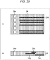
- Figs. 20A and 20B are diagrams explaining punching of the flexible substrate 54.
- Fig. 20A is a plan view illustrating an example of punching of the flexible substrate 54.
- an end portion on the left side, in the figure, of the flexible substrate 54 is punched to thereby form openings 54e aligned in a vertical direction.
- the openings 54e are formed at positions on the surface of the flexible substrate 54 where wiring 54f is not formed.
- the flexible substrate 54 has a multilayer structure, and is formed such that four layers of substrates are layered. Further, on the uppermost substrate of the flexible substrate 54, wiring is not formed. In Fig. 20A , a plurality of lines extending in a horizontal direction in the figure schematically represent that the wiring 54f formed in the flexible substrate 54 is seen through the uppermost substrate.
- Fig. 20B is a side view corresponding to Fig. 20A .
- the opening 54e is formed so as to penetrate from the surface to the bottom face of the flexible substrate 54, and is formed at a position where wiring 54g, wiring 54h, or wiring 54i is not formed inside the flexible substrate 54. This means that all of the layers of the flexible substrate 54 having a multilayer structure are punched to thereby form the opening 54e.
- metal is embedded.
- the metal to be embedded here is Au or a metal having high connectivity with the electrode pad of the image sensor 61, for example. Further, if the thickness of the flexible substrate 54 is about 100 ⁇ m, metal to be embedded may be one in which the surface of a metal such as Ni is plated by Au, for example, rather than a single metal.
- Figs. 21A and 21B are side views explaining a connecting method between the rigid substrate 53 and the flexible substrate 54.
- metal is embedded in the opening 54e to thereby form an embedded electrode 71.
- the embedding method may be a method such as a squeegee printing, for example.
- the embedded electrode 71 is connected with an electrode pad 72 of the rigid substrate 53 through metal bonding by heat or ultrasonic waves. This means that the embedded electrode 71 is directly welded to the electrode pad 72.
- the electrode pad 72 is electrically connected with wiring 73 inside the rigid substrate 53.
- the wiring 73 of the rigid substrate 53 is connected with the wiring 54i of the flexible substrate 54, and the rigid substrate 53 and the flexible substrate 54 are attached to each other with an adhesive such as ACF, an adhesive containing solder (SAM, or the like), or the like.
- the wiring 73 of the rigid substrate 53 corresponds to a terminal of the connection terminal portion 53a, for example, and the wiring 54i of the flexible substrate 54 corresponding to a terminal of a connection terminal portion of the flexible substrate 54, for example.
- the electrode pad 61a of the image sensor 61 and the embedded electrode 71 are connected with each other by wire bonding through the wire 63. Thereby, the electrode pad 61a of the image sensor 61 and the wiring 54i of the flexible substrate 54 are connected with each other electrically.
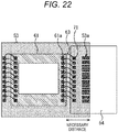
- Fig. 22 is a plan view seen from above of Figs. 21A and 21B .
- one end of a wire is connected with each of the electrode pads provided by being aligned in a vertical direction on the right side in the figure and on the left side in the figure of the image sensor 61.
- the flexible substrate 54 is attached so as to overlap the connection terminal portions 53a of the rigid substrate 53, and the other end of the wire 63, connected with the electrode pad 61a on the right side in the figure, is connected with the embedded electrode 71 embedded in the flexible substrate 54.
- a distance from the end on the right side, in the figure, of the image sensor 61 to the end on the left side, in the figure, of the flexible substrate 54 is a necessary distance.
- the electrode pads on the left side in the figure of the image sensor 61 are connected with the electrode pads of the rigid substrate 53 through wires.
- Figs. 23A and 23B are side views explaining another example of a connecting method between the rigid substrate 53 and the flexible substrate 54.
- a stud bump 81 is formed in the opening 54e.
- the stud bump 81 is connected with the electrode pad 72 of the rigid substrate 53 through metal bonding by heat or ultrasonic waves. This means that the stud bump 81 is directly welded to the electrode pad 72.
- the electrode pad 72 is electrically connected with the wiring 73 inside the rigid substrate 53.
- the wiring 73 of the rigid substrate 53 is connected with the wiring 54i of the flexible substrate 54, and the rigid substrate 53 and the flexible substrate 54 are attached to each other with an adhesive of ACF, for example.
- the electrode pad 61a of the image sensor 61 and the stud bump 81 are connected by wire bonding through the wire 63. Thereby, the electrode pad 61a of the image sensor 61 and the wiring 54i of the flexible substrate 54 are electrically connected.
- the rigid substrate 53 and the flexible substrate 54 may be overlapped and attached to each other by aligning the position of the stud bump 81 and the position of the opening 54e.
- the embedded electrode 71 or the stud bump 81 formed in the opening 54e of the flexible substrate 54 is connected with the electrode pad 72 of the rigid substrate 53, and is electrically connected with the wiring 73 inside the rigid substrate 53.
- a signal output from the image sensor 61 is transmitted from the flexible substrate 54 through the rigid substrate 53 once, and is transmitted to the flexible substrate 54 again.
- the wiring in the rigid substrate 53 can be further simplified. Further, as a signal output from the image sensor 61 is transmitted not through the connection terminal portion 53a of the rigid substrate 53, it is possible to reduce impedance associated with connection of the terminals, and further, to reduce the number of terminals in the connection terminal portions 53a.
- Fig. 24 is a side view explaining still another example of a connecting method between the rigid substrate 53 and the flexible substrate 54.
- a pad 85 is formed on the upper side in the figure of the flexible substrate 54.
- the pad 85 is wire-bonded to the electrode pad 61a of the image sensor 61 through the wire 63, and a signal output from the image sensor 61 is transmitted inside the flexible substrate 54 through the wiring 54j and the like.
- Fig. 25 which is part of Fig. 24 , is a diagram illustrating an enlarged connecting portion between the flexible substrate 54 and the rigid substrate 53.
- a signal supplied through the wire 63 connected with the pad 85 is transmitted inside the flexible substrate 54 through the wiring 54j and the like, not through the rigid substrate 53.
- a signal transmitted through the wiring and the like in the rigid substrate 53 is transmitted to the flexible substrate 54, by the wiring 73 (terminal of the connection terminal portion 53a) of the rigid substrate 53 and the wiring 54i (terminal of the connection terminal portion) of the flexible substrate being connected with each other with ACF, an adhesive containing solder, or the like.
- the pad 85 in the flexible substrate 54 having a multilayer structure, the pad 85 may be formed by forming an opening by punching an end portion of the uppermost layer, and embedding metal in the opening, for example. In this step, metal is embedded in the opening by squeegee printing or the like.
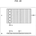
- Figs. 26A and 26B are diagrams explaining punching of the flexible substrate 54 when forming the pad 85 illustrated in Fig. 25 .
- Fig. 26A is a plan view illustrating an example of punching of the flexible substrate 54.
- an end portion on the left side, in the figure, of an uppermost layer 54-1 of the flexible substrate 54 is punched to thereby form openings 54-1e aligned in a vertical direction.
- Fig. 26B is a side view corresponding to Fig. 26A . As illustrated in the figure, the opening 54-1e is formed so as to penetrate only the uppermost layer 54-1 of the flexible substrate 54.
- Figs. 27A and 27B are diagrams illustrating a configuration of the entire flexible substrate 54 configured to include the uppermost layer 54-1 illustrated in Fig. 26A and Fig. 26B .
- Fig. 27A is a plan view of the entire flexible substrate 54 configured to include the uppermost layer 54-1.
- the flexible substrate 54 has a four-layer structure.
- the uppermost layer 54-1 adheres to the other three layers, and a plurality of lines extending in a horizontal direction in the figure schematically represent that the wiring 54f formed in the flexible substrate 54 is seen through the uppermost substrate.
- Fig. 27B is a side view corresponding to Fig. 27A . As illustrated in the figure, the opening 54-1e only penetrates the uppermost layer 54-1 of the flexible substrate 54, and no opening is formed in the lower layers.
- the wiring in the rigid substrate 53 can be further simplified.
- connection terminal portion 53a of the rigid substrate 53 As a signal output from the image sensor 61 is transmitted not through the connection terminal portion 53a of the rigid substrate 53, it is possible to reduce impedance associated with connection of the terminal, and further, to reduce the number of terminals in the connection terminal portion 53a.
- the pad 85 as illustrated in Fig. 25 and the embedded electrode 71 as illustrated in Figs. 21A and 21B (or the stud bump 81 as illustrated in Figs. 23A and 23B ) may be formed so as to be provided together.
- the pad 85 is formed, impedance associated with connection of the terminal can be reduced.
- a wire for a signal having high resistance to noise is allowed to be connected with the embedded electrode 71 or the stud bump 81, and the other wires for a signal are allowed to be connected to the pad 85, for example.
- the pad 85 and the embedded electrode 71 (or stud bump 81) are provided together, it is possible to improve the bonding strength between the rigid substrate 53 and the flexible substrate 54 without lowering the SI (Signal Integrity).
- On bump bonding is a form in which a bump is formed on an electrode pad in advance, and second bonding is performed on the bump.
- the size of the camera module by adopting another method.
- one end of the wire 63 is connected with each of the electrode pads (squares in the figure) provided to be aligned in a vertical direction on the right side in the figure and on the left side in the figure of the image sensor 61. Further, the other end of the wire 63 is connected with each of the electrode pads (squares in the figure) provided to be aligned in a vertical direction on the right side in the figure and on the left side in the figure of the rigid substrate 53.
- each of the electrode pads provided to be aligned on the right side, in the figure, of the rigid substrate is an electrode pad 53b.
- Fig. 28 is an enlarged view of part of the electrode pads 53b and the connection terminal portion 53a in Fig. 18A .
- Fig. 28 illustrates electrode pads 53b-1 to 53b-5, and terminals 53a-1 to 53a-5 in the connection terminal portion 53a.
- the electrode pad 53b-1 is connected with the wiring inside (in the lower layer of) the rigid substrate 53 through a via V11, and is connected with a via, not shown, through the wiring, to thereby be electrically connected with a terminal connected with the via. Further, the terminal 53a-1 is connected with the wiring inside (in the lower layer of) the rigid substrate 53 through a via V21, and is connected with an electrode pad or the like, not shown, through the wiring.
- the electrode pad 53b-2 is directly connected with the terminal 53a-2 through the wiring in the surface layer of the rigid substrate 53 to thereby be electrically connected with the terminal 53a-2.
- the electrode pad 53b-3 is directly connected with the terminal 53a-3 through the wiring in the surface layer of the rigid substrate 53 to thereby be electrically connected with the terminal 53a-3.
- the electrode pad 53b-4 is connected with the wiring inside (in the lower layer of) the rigid substrate 53 through a via V12, and is connected with a via, not shown, through the wiring, to thereby be electrically connected with a terminal connected with the via. Further, the terminal 53a-4 is connected with the wiring inside (in the lower layer of) the rigid substrate 53 through a via V22, and is connected with an electrode pad or the like, not shown, through the wiring.
- the electrode pad 53b-5 is directly connected with the terminal 53a-3 through the wiring in the surface layer of the rigid substrate 53 to thereby be electrically connected with the terminal 53a-5.
- a necessary distance which is a distance corresponding to the overlap width and the width for wire bonding, from an end of the rigid substrate 53, also becomes longer.
- the electrode pads provided to be aligned in a vertical direction of the rigid substrate 53 and the terminals in the connection terminal portion 53a are made common, for example.
- the electrode pads provided at positions near the connection terminal portion 53a and aligned in a vertical direction on the right side, in the figure, of the rigid substrate 53 are made common to the terminals in the connection terminal portion 53a.
- the terminals in the connection terminal portion 53a are classified into three, in which a terminal group provided on the upper side in the figure is a terminal group Tm1, a terminal group provided in the middle in the figure is a terminal group Tm2, and a terminal group provided on the lower side in the figure is a terminal group Tm3.
- a terminal group which is made common to the electrode pads provided to be aligned in a vertical direction on the right side in the figure of the rigid substrate 53 is the terminal group Tm2.
- the terminal group Tm1 and the terminal group Tm3 are not made common to the electrode pads provided to be aligned in a vertical direction on the right side in the figure of the rigid substrate 53.
- Fig. 30 is an enlarged view of part of the terminal group Tm2 in Fig. 29 .
- Fig. 30 illustrates the terminals 53a-1 to 53a-5 in the connection terminal portion 53a.
- the terminals 53a-1 to 53a-5 in Fig. 30 are terminals having larger areas compared with the case of the terminals 53a-1 to 53a-5 in Fig. 28 .
- the other end of the wire 63 in which one end thereof is connected with the electrode pad of the image sensor 61, is wire bonded.
- a connection terminal of the flexible substrate 54 is attached to each of the terminals 53a-1 to 53a-5.
- the terminal 53a-5 is configured to be connected with the wiring inside (in the lower layer of) the rigid substrate 53 through a via V23.
- the terminal 53a-5 is, for example, a terminal of a power source or GND, and is connected with the power source or the GND through the wiring inside (in the lower layer of) the rigid substrate 53.
- Fig. 31 is a cross-sectional view corresponding to Fig. 18B , and is a cross-sectional view taken along a line in a horizontal direction in the figure passing through the center of the image sensor 61 in Fig. 18B .
- one end of the wire 63 is connected with the electrode pad on the image sensor 61, and the other end of the wire 63 is connected with the electrode pad 53b of the rigid substrate 53.
- Fig. 32 is a cross-sectional view corresponding to Fig. 29 , and is a cross-sectional view taken along a line in a horizontal direction in the figure passing through the center of the image sensor 61 in Fig. 18B .
- one end of the wire 63 is connected with the electrode pad on the image sensor 61, and the other end of the wire 63 is connected with the terminal in the connection terminal portion 53a on the rigid substrate 53.
- the electrode pads (electrode pad 53b in Fig. 31 ) provided to be aligned on the right side in the figure of the rigid substrate 53 are made common to the terminals of the connection terminal portion 53a.
- a length L22 in a horizontal direction in the figure of the rigid substrate 53, in the configuration illustrated in Fig. 32 is shorter than a length L21 in a horizontal direction in the figure of the rigid substrate 53 in the configuration illustrated in Fig. 31 .
- a necessary distance which is a distance from an end of the rigid substrate 53 corresponding to the overlap width and the width for wire bonding can also be shortened.
- the size of a camera module can be further reduced.
- a camera module to which the present technology is applied is to be installed in an electronic device such as a mobile telephone, a smartphone, or the like.
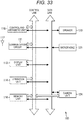
- Fig. 33 is a block diagram illustrating an exemplary inner configuration according to an embodiment of a mobile telephone to which the present technology is applied.
- a communication antenna 112 is a built-in antenna, for example, and performs transmission and reception of signal wave for telephone calls and packet communications such as e-mails.
- a communication circuit 111 performs frequency conversion, modulation, and demodulation of transmission/reception signals.
- a speaker 120 is a speaker for receiving voices provided in the mobile telephone 100, or a speaker for outputting ringer (incoming calls), alarm sound, and the like, and converts sound signals supplied from a control and arithmetic unit 110 into acoustic waves and outputs them to the air.
- a microphone 121 is a microphone for voice transmission and collection of outside sound, and converts acoustic waves to sound signals and transmits the sound signals to the control and arithmetic unit 110.
- a display unit 113 includes a display device such as a liquid crystal display or an organic EL display, and a display drive circuit of the display, and displays various types of characters and images such as e-mails, for example, on the display by image signals supplied from the control and arithmetic unit 110, and if captured images are supplied from the camera unit 124, displays the captured images.
- a display device such as a liquid crystal display or an organic EL display
- a display drive circuit of the display and displays various types of characters and images such as e-mails, for example, on the display by image signals supplied from the control and arithmetic unit 110, and if captured images are supplied from the camera unit 124, displays the captured images.
- An operation unit 114 is configured of various keys such as numeric keys, a call key, an end/power key, and the like provided on the casing of the mobile telephone 100, various operators such as a cross key, a shutter button, and a horizontal photographing mode switch, and an operation signal generator which generates operation signals when those operators are operated. It should be noted that if the mobile telephone 100 has a touch panel, the touch panel is also included in the operation unit 114.
- a camera unit 124 is a function block equivalent to the camera module 50 described above with reference to Figs. 4 to 16 . This means that as the camera unit 124, the camera module 50 to which the present technology is applied is disposed. An image signal captured by the camera unit 124 is applied with various types of image processing by the control and arithmetic unit 110, and then, is displayed on the display screen of the display unit 113, is compressed and stored in a memory unit 116, or the like.
- the memory unit 116 includes a built-in memory provided inside the terminal, and a detachable card memory which stores so-called SIM (Subscriber Identity Module) information and the like.
- the built-in memory includes a ROM (Read Only Memory) and a RAM (Random Access Memory).
- a ROM is configured of a rewritable ROM such as a NAND-type flash memory or an EEPROM (Electrically Erasable Programmable Read-Only Memory).
- an OS Operating System
- control program for controlling the respective units by the control and arithmetic unit 110
- various application programs dictionary data
- sound data such as incoming call sound and key operation sound
- image data captured by the camera unit 124 and the like are stored.
- a RAM stores data from time to time, as a work region when the control and arithmetic unit 110 performs various types of data processing.
- the control and arithmetic unit 110 is configured of a CPU (central processing unit), and performs control of communications in the communication circuit 111, sound processing and control thereof, image processing and control thereof, control of image capturing by the camera unit 124, control of other various types of signal processing and respective units, and the like. Further, the control and arithmetic unit 110 performs execution of various types of control programs and application programs stored in the memory unit 116, and various types of data processing associated therewith, and the like.
- components provided to a typical mobile telephone 100 which includes a current position detection unit using GPS (Global Positioning System) satellite waves, a contactless communication unit which performs contactless communications used in a contactless IC card, and the like, a power management IC unit which controls a battery for supplying power to respective units and the power thereof, a slot for external memory, a receiving tuner for digital broadcasting, an AV codec unit, and the like.
- GPS Global Positioning System
- a camera module to which the present technology is applied, is installed in a mobile telephone
- a camera module to which the present technology is applied, can be installed in various types of electronic devices such as a smartphone and a tablet device.
Landscapes
- Engineering & Computer Science (AREA)
- Multimedia (AREA)
- Signal Processing (AREA)
- Studio Devices (AREA)
- Camera Bodies And Camera Details Or Accessories (AREA)
Description
- The present technology relates to a camera module and an electronic device, and in particular, to a camera module in which a thin camera module can be realized at a low cost and an electronic device.
- In a conventional camera module structure, FPC (Flexible Printed Circuits) are disposed on the lower side of a module and are connected by soldering or by ACF (Anisotropic Conductive Film) (for example, see Patent Document 1).
- As such, the thickness of the FPC and the thickness of the connecting portion (solder connection or ACF connection) are included in the height of the module such as a lens unit, whereby there is a problem that the thickness of the module increases.
- Meanwhile, a rigid flexible substrate, in which a rigid portion and a flexible portion are integrated, may also be used. In that case, there is no need to take into account a connection between the rigid substrate and the FPC.
- Patent Document 1: Japanese Patent Application Laid-Open No.
2009-033481 - However, in the case of using a rigid flexible substrate, constraints on the design increases, compared with the case of a configuration in which a rigid substrate and FPC are connected, for example.
- For example, in the case of using a rigid flexible substrate, as it is necessary to conform the pitch of vias and the width of wiring to design rules of the flexible portion in the substrate, it is difficult to perform fine wiring in the rigid portion in the substrate.
- Further, in the case of using a rigid flexible substrate, as a layer constituting the flexible portion is inserted between layers constituting the rigid portion, a range of process conditions such as an ultrasonic wave, temperature setting, and the like becomes narrow when an image sensor is wire-bonded, and the like.
- Further, in the case of using a rigid flexible substrate, as a member usage rate decreases in each of the layer constituting the rigid portion and the layer constituting the flexible portion, the substrate cost increases. As such, it is difficult to suppress the cost of the entire camera module.
- Further, in the case of using a rigid flexible substrate, when attempting to change the shape of the flexible portion corresponding to a device (mobile telephone, smartphone, or the like) in which the camera module is incorporated, for example, it is necessary to redesign the entire substrate including the rigid portion. As such, the delivery period of the substrate becomes longer, for example, and the cost further increases.
-
US 2006/0091487 A1 relates to a manufacturing method of a solid state image sensing device and to such a solid state image sensing device to be used for a mobile communication device in which a wiring substrate protrudes from the bottom surface of a lens unit to thereby allow a flexible substrate to be attached on the upper side of the surface of wiring substrate carrying the lens unit. -
US 2011/0002685 A1 discloses a similar device wherein a base plate carries a circuit board on which a lens unit is mounted. - The present technology is disclosed in view of such a situation, and aims to realize a thin camera module at a low cost.
- According to a first aspect the invention provides a camera module in accordance with
claim 1. Further aspects of the invention are set forth in the dependent claims, the drawings and the following description of embodiments. - According to the present technology, a thin camera module can be realized at a low cost.
-
-
Fig. 1 is a perspective view illustrating an exemplary configuration of a conventional camera module. -
Fig. 2 is a side view explaining an exemplary configuration of a conventional camera module. -
Fig. 3 is a side view illustrating an exemplary configuration of a modification of the camera module illustrated inFig. 2 . -
Fig. 4 is a side view explaining an exemplary configuration of a camera module to which the present technology is applied. -
Figs 5A and 5B are another side views explaining an exemplary configuration of a camera module to which the present technology is applied. -
Fig. 6 is a plan view of the camera module illustrated inFigs 5A and 5B , seen from the upper direction ofFigs 5A and 5B . -
Fig. 7 is another plan view of the camera module illustrated inFigs 5A and 5B , seen from the upper direction ofFigs 5A and 5B . -
Fig. 8 is a plan view illustrating a detailed exemplary configuration of a frame ofFig. 7 . -
Fig. 9 is a cross-sectional view of the frame taken along an alternate long and short dash line A-A' ofFig. 8 . -
Fig. 10 is a plan view illustrating another detailed exemplary configuration of the frame ofFig. 7 . -
Fig. 11 is a cross-sectional view of the frame taken along an alternate long and short dash line A-A' ofFig. 10 . -
Fig. 12 is a plan view of the camera module illustrated inFigs 5A and 5B , seen from the upper direction ofFigs 5A and 5B . -
Fig. 13 is a plan view illustrating a configuration of a flexible substrate and a rigid substrate, illustrated inFig. 12 , in detail. -
Figs. 14A to 14F are diagrams illustrating an exemplary manufacturing process of a camera module to which the present technology is applied. -
Fig. 15 is a diagram explaining another configuration of a flexible substrate in a camera module to which the present technology is applied. -
Fig. 16 is a diagram explaining still another configuration of a flexible substrate in a camera module to which the present technology is applied. -
Fig. 17 is a side view explaining a necessary distance which is a distance from an end of an image sensor to an end of a rigid substrate. -
Figs. 18A and 18B are plan views seen from above ofFig. 17 . -
Fig. 19 is a diagram illustrating an example in which an electrode pad of an image sensor and a flexible substrate are directly connected with each other. -
Figs. 20A and 20B are diagrams explaining punching of a flexible substrate. -
Figs. 21A and 21B are side views explaining a method of connecting a rigid substrate and a flexible substrate. -
Fig. 22 is a plan view seen from above ofFigs. 21A and 21B . -
Figs. 23A and 23B are side views explaining another example of a method of connecting a rigid substrate and a flexible substrate. -
Fig. 24 is a side view explaining still another example of a method of connecting a rigid substrate and a flexible substrate. -
Fig. 25 is a diagram illustrating an enlarged connecting portion between the flexible substrate and the rigid substrate ofFig. 24 . -
Figs. 26A and 26B are diagrams explaining punching of the uppermost layer of a flexible substrate. -
Figs. 27A and 27B are diagrams explaining a configuration of the entire flexible substrate configured by including the uppermost layer illustrated inFigs. 26A and 26B . -
Fig. 28 is an enlarged view of part of electrode pads and a connection terminal portion inFig. 18A . -
Fig. 29 is a diagram illustrating an example in which an electrode pad of a rigid substrate and a terminal of a connection terminal unit are made common. -
Fig. 30 is an enlarged view of part of a terminal group ofFig. 29 . -
Fig. 31 is a cross-sectional view corresponding toFig. 18B . -
Fig. 32 is a cross-sectional view corresponding toFig. 29 . -
Fig. 33 is a block diagram illustrating an exemplary inner configuration according to an embodiment of a mobile telephone to which the present technology is applied. - Hereinafter, embodiments of the technology disclosed herein will be described with reference to the drawings.
-
Fig. 1 is a perspective view illustrating an exemplary configuration of a conventional camera module. Acamera module 10 illustrated in the figure is to be installed in an electronic device such as a mobile telephone or a smartphone. - The
camera module 10 inFig. 1 is configured of alens unit 11, aframe 12, arigid substrate 13, and aflexible substrate 14. A flexible substrate is also referred to as FPC (Flexible Printed Circuits). - The
lens unit 11 is a unit which stores a lens of the camera, and the like. Light condensed through the lens in thelens unit 11 forms an image on a light receiving surface of an image sensor, described below, whereby an image is captured. - The
frame 12 is a standardized connecting component to be used for connection with therigid substrate 13, for example, and is also used for improving shielding property, and the like. It should be noted that theframe 12 may not be provided. In that case, thelens unit 11 is directly attached to therigid substrate 13. - The
rigid substrate 13 is a substrate on which an image sensor of the camera is disposed, for example. - The
flexible substrate 14 is a substrate on which wiring for inputting and outputting signals, input or output to/from thecamera module 10, to/from another unit of an electronic device is printed, for example. In the example ofFig. 1 , theflexible substrate 14 is attached to the bottom surface (surface on the lower side in the figure) of therigid substrate 13. -
Fig. 2 is a side view explaining an exemplary configuration of theconventional camera module 10. It should be noted that in thecamera module 10 illustrated inFig. 2 , theframe 12 inFig. 1 is not provided and thelens unit 11 is directly attached to therigid substrate 13. - Further, in the example of
Fig. 2 , theflexible substrate 14 is attached to the bottom surface of therigid substrate 13, which is the same as the case explained with reference toFig. 1 . It should be note that in this example,solder balls 21 used for attaching theflexible substrate 14 and therigid substrate 13 are illustrated. - The thickness (height in the figure) of the
camera module 10, configured as illustrated inFig. 2 , is represented as H1, and the height H1 includes the thickness of theflexible substrate 14 and the thickness of thesolder ball 21. Further, the length, in a horizontal direction in the figure, of thecamera module 10 is represented as L1. It should be noted that in this example, the length in the horizontal direction of thecamera module 10 does not include a portion where only theflexible substrate 14 exists. - However, as mobile telephones and smartphones are getting thinner increasingly in recent years, it is natural that thinner camera modules are also expected.
- As such, it is considered to use a rigid flexible substrate in which a rigid portion and a flexible portion are integrated, for example. In that case, it is not necessary to consider connection between the rigid substrate and the flexible substrate.
- However, in the case of using a rigid flexible substrate, constraints on the design increases, compared with the case of a configuration in which a rigid substrate and a flexible substrate are connected (attached) with each other.
- For example, in the case of using a rigid flexible substrate, as it is necessary to conform the pitch of vias and the width of wiring to the design rules of the flexible portion in the substrate, it is difficult to perform fine wiring in the rigid portion in the substrate.
- Further, in the case of using a rigid flexible substrate, as a layer constituting the flexible portion is inserted between layers constituting the rigid portion, a range of process conditions such as an ultrasonic wave, temperature setting, and the like becomes narrow when an image sensor is wire-bonded.
- Further, in the case of using a rigid flexible substrate, as a member usage rate decreases in each of the layer constituting the rigid portion and the layer constituting the flexible portion, the substrate cost increases. As such, it is difficult to suppress the cost of the entire camera module.
- Further, in the case of using a rigid flexible substrate, when attempting to change the shape of the flexible portion corresponding to a device (mobile telephone, smartphone, or the like) in which the camera module is incorporated, for example, it is necessary to redesign the entire substrate including the rigid portion. In that case, the delivery period of the substrate becomes longer, for example, and the cost further increases.
- Meanwhile, as illustrated in
Fig. 3 , therigid substrate 13 may be configured to protrude from the bottom surface of thelens unit 11 in order to reduce the thickness of the entire module to thereby allow theflexible substrate 14 to be attached on the surface (surface on the upper side in the figure) of therigid substrate 13. - In the case of configuring the
camera module 10 as illustrated inFig. 3 , as the thickness of theflexible substrate 14 and the thickness of thesolder ball 21 are canceled, the thickness of thecamera module 10 is H2, which is less than H1. As such, it is possible to configure thecamera module 10 to be thinner, compared with the case ofFig. 1 . - However, in the case of configuring the
camera module 10 as illustrated inFig. 3 , as therigid substrate 13 extends in a horizontal direction in the figure by a length α, the length of the entire camera module in the horizontal direction in the figure also extends. In the example ofFig. 3 , the length of thecamera module 10 in the horizontal direction in the figure is L2 which is larger than L1. - As such, in the case of configuring the
camera module 10 as illustrated inFig. 3 , for example, a mobile telephone, a smartphone, or the like must be designed while taking into account an increase in the length of thecamera module 10 in the horizontal direction. - In view of the above, the present technology configures a camera module as illustrated in
Fig. 4 , for example. -
Fig. 4 is a side view explaining an exemplary configuration of acamera module 50 to which the present technology is applied. It should be noted that in thecamera module 50 illustrated inFig. 4 , the frame described inFig. 1 is not provided, and alens unit 51 is directly attached to therigid substrate 53. - Further, in the
camera module 50 illustrated inFig. 4 , a left end portion, in the figure, of aflexible substrate 54 is interposed between thelens unit 51 and therigid substrate 53. - The
camera module 50, to which the present technology is applied, is configured such that only an end portion on the left side, in the figure, of theflexible substrate 54 is attached to an end portion on the right side, in the figure, of the surface of therigid substrate 53. Further, in thecamera module 50 to which the present technology is applied, a groove for accommodating the left end portion of theflexible substrate 54 is provided on an end portion on the right side, in the figure, of thelens unit 51, the details of which will be described below. - In the case of configuring the
camera module 50 as illustrated inFig. 4 , as the thickness of theflexible substrate 54 and the thickness of the solder ball are canceled, the thickness of thecamera module 50 is H2. As such, it is possible to configure the camera module to be thinner, compared with the case ofFig. 1 . - Further, in the case of configuring the
camera module 50 as illustrated inFig. 4 , the length of thecamera module 50 in the horizontal direction in the figure is L1. Accordingly, the length of the entire camera module in the horizontal direction in the figure does not extend, as in the configuration illustrated inFig. 3 . - Further, in the case of configuring the
camera module 50 as illustrated inFig. 4 , the length of theflexible substrate 54 in the horizontal direction in the figure can be configured to be shorter. For example, theflexible substrate 54 inFig. 4 is configured to have a length shorter by a length L3 in the horizontal direction in the figure, compared with the case of theflexible substrate 14 inFig. 1 , for example. - Accordingly, in the case of configuring the
camera module 50 as illustrated inFig. 4 , the area of the flexible substrate can be reduced by the amount corresponding to the length L3, compared with the configuration ofFig. 1 . This means that by applying the present technology, the area of an expensive flexible substrate is reduced, whereby the cost of the entire camera module can also be reduced. -
Figs 5A and 5B are another side views explaining an exemplary configuration of thecamera module 50 to which the present technology is applied.Fig. 5A is a diagram illustrating an exemplary configuration on the case where a frame is not provided in thecamera module 50, andFig. 5B is a diagram illustrating an exemplary configuration of the case where a frame is provided in thecamera module 50. - In the
camera module 50 illustrated inFig. 5A , a left end portion, in the figure, of theflexible substrate 54 is interposed between thelens unit 51 and therigid substrate 53. - The
camera module 50, to which the present technology is applied, is configured such that only an end portion on the left side, in the figure, of theflexible substrate 54 is attached to an end portion on the right side, in the figure, of the surface of therigid substrate 53. Further, in the example ofFig. 5A , agroove 51a for accommodating the left end portion of theflexible substrate 54 is formed in an end portion on the right side, in the figure, of thelens unit 51. - In the
camera module 50 illustrated inFig. 5B , aframe 52 is provided between thelens unit 51 and therigid substrate 53, and a left end portion, in the figure, of theflexible substrate 54 is interposed between theframe 52 and therigid substrate 53. Further, in the example ofFig. 5B , agroove 52a for accommodating the left end portion of theflexible substrate 54 is formed in an end portion on the right side, in the figure, of theframe 52. - If the
groove 51a or thegroove 52a is not formed, for example, the right side in the figure of thelens unit 51 floats due to the thickness of theflexible substrate 54, whereby there is a possibility that the light condensed by the lens in thelens unit 51 does not form an image appropriately on the imaging surface of the image sensor on therigid substrate 53. Here, in order to allow the light condensed by the lens to form an image appropriately on the imaging surface of the image sensor, it is necessary that the parallel degree of the top surface (surface on the upper side in the figure) of thelens unit 51 and the imaging surface of theimage sensor 61 becomes 1.5 degrees or smaller. - It should be noted that as the
lens unit 51 or theframe 52 is attached to therigid substrate 53 with an adhesive or the like, by adjusting the thickness of the adhesive, for example, it is possible to perform tilt adjustment so as to set the focus position of the lens in thelens unit 51 to be appropriate. - Further, if the
groove 51a or thegroove 52a is not formed, the right side, in the figure, of thelens unit 51 floats due to the thickness of theflexible substrate 54. As such, the adhesive must be injected in extra amounts for that portion, into a left-side portion in the figure. As such, the attachment strength of thelens unit 51 or theframe 52 may be insufficient, or light transmitted through the adhesive may leak in the image sensor. - However, if an adhesive having high shielding property is injected in a large amount in such a manner that the surface of the
rigid substrate 53 and the bottom surface of the lens unit 51 (or the frame 52) become parallel to each other in a state where theflexible substrate 54 is interposed, the camera module may be configured without forming thegroove 51a or thegroove 52a. -
Fig. 6 is a plan view of thecamera module 50 illustrated inFigs 5A and 5B , viewed from the upper direction ofFigs 5A and 5B . It should be noted that inFig. 6 , thelens unit 51 and theframe 52 are not illustrated for easy understanding. - As illustrated in
Fig. 6 , arectangle image sensor 61 is disposed on the almost center of therigid substrate 53. It should be noted that in the figure, the front side of the sheet is the imaging surface of theimage sensor 61. As illustrated in the figure, a portion on the left side, in the figure, of theflexible substrate 54 overlaps a portion on the right side, in the figure, of therigid substrate 53. In the overlapped portion, theflexible substrate 54 and therigid substrate 53 are attached, or electrically connected, to each other. - Further, as illustrated in
Fig. 6 , theflexible substrate 54 is disposed on the rigid substrate 53 (on the light receiving side of the image sensor 61). -
Fig. 7 is another plan view of thecamera module 50 illustrated inFigs 5A and 5B , viewed from the upper direction ofFigs 5A and 5B . In the case ofFig. 7 , an illustration of theframe 52 is added, which is different fromFig. 6 . - As illustrated in
Fig. 7 , a portion on the left side, in the figure, of theflexible substrate 54 overlaps a portion on the right side, in the figure, of theframe 52, and theflexible substrate 54 is disposed under theframe 52. Further, the center of theframe 52 is formed as a cavity, whereby the imaging surface of theimage sensor 61 is seen. -
Fig. 8 is a plan view illustrating a detailed exemplary configuration of theframe 52 ofFig. 7 . This figure is a diagram illustrating theframe 52 seen from the lower direction (rear side of the sheet) ofFig. 7 , in which the bottom surface of theframe 52 is illustrated. As illustrated inFig. 8 , thegroove 52a is formed on the right side, in the figure, of theframe 52. It should be noted that the center portion of theframe 52 is formed as a cavity, as described above. -
Fig. 9 is a cross-sectional view of theframe 52 taken along the alternate long and short dash line A-A' ofFig. 8 . As illustrated in the figure, thegroove 52a is formed on the right side in the figure. -
Fig. 10 is a plan view illustrating another detailed exemplary configuration of theframe 52 ofFig. 7 . This figure is a diagram illustrating theframe 52 seen from the lower direction ofFig. 7 , in which the bottom surface of theframe 52 is illustrated. As illustrated inFig. 10 , thegroove 52a is formed on the right side, in the figure, of theframe 52. It should be noted that the center portion of theframe 52 is formed as a cavity, as described above. - In the example of
Fig. 10 , thegroove 52a is formed across therigid substrate 53 from the top to the bottom in the figure, which is different from the case ofFig. 8 . Thegroove 52a may be formed in this way. -
Fig. 11 is a cross-sectional view of theframe 52, taken along the alternate long and short dash line A-A' ofFig. 10 . As illustrated in the figure, thegroove 52a is formed on the right side in the figure. - It should be noted that while the case where the
groove 52a is formed in theframe 52 has been described herein, this also applies to the case where thegroove 51a is formed in thelens unit 51. This means that thegroove 51a may be formed across theentire lens unit 51 from the top to the bottom as in the case ofFig. 10 , or thegroove 51a may be formed in such a manner that the upper side and the lower side of thelens unit 51 are left, as in the case ofFig. 8 . - Meanwhile, on the surface of the
rigid substrate 53, a solder resist (SR) serving as an insulation film protecting the circuit pattern, for example, is provided. However, as described with reference toFigs. 5 to 11 , in the case of attaching theflexible substrate 54 to the surface of therigid substrate 53 so as to be electrically connected with each other, the SR must be removed beforehand in a portion of the surface of therigid substrate 53, in order to connect a connection terminal of theflexible substrate 54 and a connection terminal of therigid substrate 53 with each other. -
Fig. 12 is a plan view of thecamera module 50 illustrated inFigs 5A and 5B , viewed from the upper direction ofFigs 5A and 5B . It should be noted that inFig. 12 , thelens unit 51 and theframe 52 are not illustrated for easy understanding. - As illustrated in
Fig. 12 , therectangle image sensor 61 is disposed on the almost center of therigid substrate 53. As illustrated in the figure, a portion on the left side, in the figure, of theflexible substrate 54 overlaps a portion on the right side, in the figure, of therigid substrate 53. In a portion on the right side, in the figure, of therigid substrate 53, the SR is removed and aconnection terminal portion 53a is formed. - Further, even in the
flexible substrate 54, a connection terminal portion is formed in a portion on the left side in the figure. However, inFig. 12 , as a connection terminal portion is provided on the rear face of theflexible substrate 54, it is not illustrated. - The
connection terminal portion 53a of therigid substrate 53 and the connection terminal portion, not illustrated, of theflexible substrate 54 are provided with connection terminals, respectively, and the connection terminal of therigid substrate 53 of therigid substrate 53 and the connection terminal of theflexible substrate 54 are attached, whereby therigid substrate 53 and theflexible substrate 54 are connected electrically. -
Fig. 13 is a plan view illustrating the configuration of theflexible substrate 54 and therigid substrate 53 illustrated inFig. 12 , in detail. In the example of the figure, theimage sensor 61 is illustrated in more detail. Further, a portion on the left side, in the figure, of theflexible substrate 54 overlaps a portion on the right side, in the figure, of therigid substrate 53. InFig. 13 , the overlapped portion is illustrated as an overlap width W. - The overlap width W is represented as a distance from an end potion of one side (e.g., a side on the right side in
Fig. 13 ) of a square rigid substrate, and in the band region of the overlap width W, theflexible substrate 54 and therigid substrate 53 are attached to each other in an overlapped manner. In order to reduce the cost of the entire camera module by preventing the connection (attachment) with theflexible substrate 54 from affecting the arrangement of theimage sensor 61 and by reducing the area of the expensive flexible substrate, the overlap width W is desirably 2.4 mm or less, for example. -
Figs. 14A to 14F are diagrams explaining an example of a manufacturing process of a camera module to which the present technology is applied. - First, as illustrated in
Fig. 14A , therigid substrate 53, on which acomponent 62 is mounted, is prepared. It should be noted that as described with reference toFig. 12 , the SR is removed in a portion on the right side, in the figure, of therigid substrate 53, and theconnection terminal portion 53a is formed. - Next, as illustrated in
Fig. 14B , theflexible substrate 54 is attached to therigid substrate 53. In this step, therigid substrate 53 and theflexible substrate 54 are attached to each other in the overlap width W, and the connection terminal disposed in theconnection terminal portion 53a and the connection terminal of theflexible substrate 54 are attached to thereby be connected electrically. - It should be noted that for attaching the
rigid substrate 53 and theflexible substrate 54, solder, an adhesive including solder, ACF, ACP, or the like is used. - Next, as illustrated in
Fig. 14C , theimage sensor 61 is die-bonded (DB) to therigid substrate 53. - Then, as illustrated in
Fig. 14D , wire-bonding (WB) is performed between theimage sensor 61 and therigid substrate 53. InFig. 14D , awire 63 is wire-bonded. - Next, as illustrated in
Fig. 14E , an adhesive is applied. InFig. 14E , an adhesive 64 is applied to both left and right sides of therigid substrate 53. As the adhesive 64 used for adhesion between therigid substrate 53 and the lens unit 51 (or adhesion between therigid substrate 53 and the frame 52), resin which attenuates light is used. For example, black resin, resin containing filler, or the like is used as the adhesive 64. - Finally, as illustrated in
Fig. 14F , theframe 52 or thelens unit 51 is attached torigid substrate 53. It should be note that in the drawing on the left side ofFig. 14F , theframe 52 is attached to therigid substrate 53, and in the drawing on the right side, thelens unit 51 is attached to therigid substrate 53. Further, as described above, in order to allow the light condensed by the lens to form an image appropriately on the imaging surface of the image sensor, it is necessary that the parallel degree of the top surface of thelens unit 51 and the imaging surface of theimage sensor 61 is 1.5 degrees or less. - The camera module to which the present technology is applied is manufactured through this manufacturing process.
- Meanwhile, in the present technology, the
flexible substrate 54 and therigid substrate 53 are attached in the portion where a portion of theflexible substrate 54 overlaps a portion of the rigid substrate 53 (overlap width). As such, according to the usage conditions of the camera module, it may be desired to improve the break strength of theflexible substrate 54. -
Fig. 15 is a diagram explaining another configuration of theflexible substrate 54 in the camera module to which the present technology is applied. This figure is a diagram corresponding toFig. 6 , and parts corresponding to those ofFig. 6 are denoted by the same reference signs. - In the example of
Fig. 15 , a reinforcedportion 54a is provided to theflexible substrate 54. In this example, the reinforcedportions 54a, extending in a left direction in the figure, are provided to an end on the upper side and an end on the lower side, in the figure, of theflexible substrate 54. This means that in theflexible substrate 54, the reinforcedportions 54a, extending in parallel with two sides of thesquare image sensor 61, are provided. - In addition to the overlap width described above, if the
flexible substrate 54 and therigid substrate 53 are also attached to each other in the reinforcedportions 54a, the area of the attached surface increases, compared with the case ofFig. 6 . Accordingly, in the case of the configuration ofFig. 15 , it is possible to improve the break strength of theflexible substrate 54, compared with the case ofFig. 6 . - Further, as the reinforced
portions 54a are provided at positions where they are not brought into contact with theimage sensor 61, they do not affect the arrangement of theimage sensor 61. - By configuring the
flexible substrate 54 as illustrated inFig. 15 , it is possible to improve the break strength of theflexible substrate 54 according to the usage conditions of the camera module, for example. - Alternatively, the
flexible substrate 54 in the camera module to which the present technology is applied may be configured as illustrated inFig. 16 . This figure is a diagram corresponding toFig. 6 , and the parts corresponding to those ofFig. 6 are denoted by the same reference signs. - In the example of
Fig. 16 , a reinforcedportion 54b is provided to theflexible substrate 54. In this example, the reinforcedportions 54b, extending in an up and down direction in the figure, are provided to an end portion on the upper side and an end portion on the lower side, in the figure, of theflexible substrate 54. This means that in theflexible substrate 54, the reinforcedportions 54b, extending in parallel with one side of thesquare image sensor 61, are provided. - In addition to the overlap width described above, if the
flexible substrate 54 and therigid substrate 53 are attached to each other in the reinforcedportions 54b, the area of the attached surface increases, compared with the case ofFig. 6 . Accordingly, in the case of the configuration ofFig. 16 , it is possible to improve the break strength of theflexible substrate 54, compared with the case ofFig. 6 . - Further, as the reinforced
portions 54b are provided at positions where they are not brought into contact with theimage sensor 61, they do not affect the arrangement of theimage sensor 61. - By configuring the
flexible substrate 54 as illustrated inFig. 16 , it is possible to improve the break strength of theflexible substrate 54 according to the usage conditions of the camera module, for example. - Meanwhile, in the embodiment described above, description has been given on the premise that the
image sensor 61 and therigid substrate 53 are wire-bonded, as described with reference toFig. 14D . - The wire connected with the
image sensor 61 bonded on therigid substrate 53 is electrically connected with the connection terminal disposed on theconnection terminal portion 53a through the wiring formed on therigid substrate 53. Then, the connection terminal of therigid substrate 53 and the connection terminal of theflexible substrate 54 are attached to each other, whereby theimage sensor 61 and theflexible substrate 54 are connected electrically. - However, in the case of such a connection, there is a limitation in size reduction of the camera module. This means that when attaching the
flexible substrate 54 to therigid substrate 53, an overlap width is required as described above, and further, a width for wire bonding is also required between theimage sensor 61 and therigid substrate 53. Accordingly, therigid substrate 53 is required to be larger by the width for at least the overlap width and the wire bonding, compared with theimage sensor 61. -
Fig. 17 is a side view explaining a necessary distance which is a distance from an end of theimage sensor 61 to an end of therigid substrate 53. As illustrated inFig. 17 , a necessary distance is a distance corresponding to an overlap width and a width for wire bonding from an end of therigid substrate 53. It should be noted that in practice, a distance considering tolerance and mounting accuracy for preventing an overlap between a wire-bonding pad of therigid substrate 53 and theconnection terminal portion 53a, in addition to the overlap width and the width for wire bonding, serves as a necessary distance. -
Figs. 18A and 18B are plan views seen from above ofFig. 17 . In the figure, illustration of thelens unit 51 is omitted for easy understanding. - As illustrated in
Fig. 18A , one end of awire 63 is connected with each of electrode pads (squares in the figure) provided by being aligned in a vertical direction on the right side in the figure and on the left side in the figure of theimage sensor 61. Further, the other end of thewire 63 is connected with each of the electrode pads (squares in the figure) provided by being aligned in a vertical direction on the right side in the figure and on the left side in the figure of therigid substrate 53. - The electrode pads of the
rigid substrate 53 are connected with theconnection terminal portions 53a through the wiring formed in therigid substrate 53, respectively. - Then, as illustrated in
Fig. 18B , theflexible substrate 54 is attached, in an overlapped manner, to theconnection terminal portions 53a of therigid substrate 53. At this time, a distance from the end on the right side, in the figure, of theimage sensor 61 to the end on the left side, in the figure, of theflexible substrate 54 is a necessary distance. - If the
rigid substrate 53 is designed so as to have such a necessary distance, it is difficult to reduce the size of therigid substrate 53. Consequently, further reduction in size of the camera module is difficult. - As such, as illustrated in
Fig. 19 , it is acceptable that the other end of thewire 63, connected with the electrode pad of theimage sensor 61, is directly connected with theflexible substrate 54, for example. In the case of the connection as illustrated inFig. 19 , as the width for wire bonding can be reduced significantly, the necessary distance can be shortened compared with the case ofFig. 17 , for example. - In the case where the other end of the
wire 63, connected with the electrode pad of theimage sensor 61, is directly connected with theflexible substrate 54, an electrode pad may be formed by forming an opening by punching a portion of an end portion of theflexible substrate 54 on which wiring is not formed, and embedding metal or the like in the opening, for example. -
Figs. 20A and 20B are diagrams explaining punching of theflexible substrate 54. -
Fig. 20A is a plan view illustrating an example of punching of theflexible substrate 54. In this example, an end portion on the left side, in the figure, of theflexible substrate 54 is punched to thereby formopenings 54e aligned in a vertical direction. As illustrated in the figure, theopenings 54e are formed at positions on the surface of theflexible substrate 54 wherewiring 54f is not formed. - It should be noted that the
flexible substrate 54 has a multilayer structure, and is formed such that four layers of substrates are layered. Further, on the uppermost substrate of theflexible substrate 54, wiring is not formed. InFig. 20A , a plurality of lines extending in a horizontal direction in the figure schematically represent that thewiring 54f formed in theflexible substrate 54 is seen through the uppermost substrate. -
Fig. 20B is a side view corresponding toFig. 20A . As illustrated in the figure, theopening 54e is formed so as to penetrate from the surface to the bottom face of theflexible substrate 54, and is formed at a position wherewiring 54g,wiring 54h, orwiring 54i is not formed inside theflexible substrate 54. This means that all of the layers of theflexible substrate 54 having a multilayer structure are punched to thereby form theopening 54e. - In the
opening 54e, metal is embedded. The metal to be embedded here is Au or a metal having high connectivity with the electrode pad of theimage sensor 61, for example. Further, if the thickness of theflexible substrate 54 is about 100 µm, metal to be embedded may be one in which the surface of a metal such as Ni is plated by Au, for example, rather than a single metal. -
Figs. 21A and 21B are side views explaining a connecting method between therigid substrate 53 and theflexible substrate 54. - As illustrated in
Fig. 21A , metal is embedded in theopening 54e to thereby form an embeddedelectrode 71. The embedding method may be a method such as a squeegee printing, for example. The embeddedelectrode 71 is connected with anelectrode pad 72 of therigid substrate 53 through metal bonding by heat or ultrasonic waves. This means that the embeddedelectrode 71 is directly welded to theelectrode pad 72. - By directly welding the metals in this way, the bonding strength between the
rigid substrate 53 and theflexible substrate 54 is enhanced. - The
electrode pad 72 is electrically connected withwiring 73 inside therigid substrate 53. Thewiring 73 of therigid substrate 53 is connected with thewiring 54i of theflexible substrate 54, and therigid substrate 53 and theflexible substrate 54 are attached to each other with an adhesive such as ACF, an adhesive containing solder (SAM, or the like), or the like. - Here, the
wiring 73 of therigid substrate 53 corresponds to a terminal of theconnection terminal portion 53a, for example, and thewiring 54i of theflexible substrate 54 corresponding to a terminal of a connection terminal portion of theflexible substrate 54, for example. - Then, as illustrated in
Fig. 21B , theelectrode pad 61a of theimage sensor 61 and the embeddedelectrode 71 are connected with each other by wire bonding through thewire 63. Thereby, theelectrode pad 61a of theimage sensor 61 and thewiring 54i of theflexible substrate 54 are connected with each other electrically. -
Fig. 22 is a plan view seen from above ofFigs. 21A and 21B . - As illustrated in
Fig. 22 , one end of a wire is connected with each of the electrode pads provided by being aligned in a vertical direction on the right side in the figure and on the left side in the figure of theimage sensor 61. Theflexible substrate 54 is attached so as to overlap theconnection terminal portions 53a of therigid substrate 53, and the other end of thewire 63, connected with theelectrode pad 61a on the right side in the figure, is connected with the embeddedelectrode 71 embedded in theflexible substrate 54. In this case, a distance from the end on the right side, in the figure, of theimage sensor 61 to the end on the left side, in the figure, of theflexible substrate 54 is a necessary distance. - It should be noted that in
Fig. 22 , the electrode pads on the left side in the figure of theimage sensor 61 are connected with the electrode pads of therigid substrate 53 through wires. - With this configuration, as the width for wire bonding can be reduced significantly, the necessary distance can be shortened, compared with the case of
Figs. 18A and 18B , for example. Thereby, it is possible to further reduce the size of the camera module. - In the example described above with reference to
Figs. 21A and 21B , while description has been given on the example of the case where the embeddedelectrode 71 is embedded in theopening 54e of theflexible substrate 54 by a method such as squeegee printing, it is possible to form a stud bump, instead of embedding the embeddedelectrode 71. -
Figs. 23A and 23B are side views explaining another example of a connecting method between therigid substrate 53 and theflexible substrate 54. - As illustrated in
Fig. 23A , astud bump 81 is formed in theopening 54e. Thestud bump 81 is connected with theelectrode pad 72 of therigid substrate 53 through metal bonding by heat or ultrasonic waves. This means that thestud bump 81 is directly welded to theelectrode pad 72. - By directly welding the metals in this way, the bonding strength between the
rigid substrate 53 and theflexible substrate 54 is enhanced. - The
electrode pad 72 is electrically connected with thewiring 73 inside therigid substrate 53. Thewiring 73 of therigid substrate 53 is connected with thewiring 54i of theflexible substrate 54, and therigid substrate 53 and theflexible substrate 54 are attached to each other with an adhesive of ACF, for example. - Then, as illustrated in
Fig. 23B , theelectrode pad 61a of theimage sensor 61 and thestud bump 81 are connected by wire bonding through thewire 63. Thereby, theelectrode pad 61a of theimage sensor 61 and thewiring 54i of theflexible substrate 54 are electrically connected. - It should be noted that after the
stud bump 81 is formed, therigid substrate 53 and theflexible substrate 54 may be overlapped and attached to each other by aligning the position of thestud bump 81 and the position of theopening 54e. - Meanwhile, in the embodiment described above with reference to
Figs. 21 to 23 , the embeddedelectrode 71 or thestud bump 81 formed in theopening 54e of theflexible substrate 54 is connected with theelectrode pad 72 of therigid substrate 53, and is electrically connected with thewiring 73 inside therigid substrate 53. In this case, a signal output from theimage sensor 61 is transmitted from theflexible substrate 54 through therigid substrate 53 once, and is transmitted to theflexible substrate 54 again. - However, if a signal output from the
image sensor 61 is transmitted to theflexible substrate 54 and is directly transmitted inside theflexible substrate 54, the wiring in therigid substrate 53 can be further simplified. Further, as a signal output from theimage sensor 61 is transmitted not through theconnection terminal portion 53a of therigid substrate 53, it is possible to reduce impedance associated with connection of the terminals, and further, to reduce the number of terminals in theconnection terminal portions 53a. -
Fig. 24 is a side view explaining still another example of a connecting method between therigid substrate 53 and theflexible substrate 54. - In the example of
Fig. 24 , apad 85 is formed on the upper side in the figure of theflexible substrate 54. Thepad 85 is wire-bonded to theelectrode pad 61a of theimage sensor 61 through thewire 63, and a signal output from theimage sensor 61 is transmitted inside theflexible substrate 54 through thewiring 54j and the like. -
Fig. 25 , which is part ofFig. 24 , is a diagram illustrating an enlarged connecting portion between theflexible substrate 54 and therigid substrate 53. - As illustrated in
Fig. 25 , a signal supplied through thewire 63 connected with thepad 85 is transmitted inside theflexible substrate 54 through thewiring 54j and the like, not through therigid substrate 53. On the other hand, a signal transmitted through the wiring and the like in therigid substrate 53 is transmitted to theflexible substrate 54, by the wiring 73 (terminal of theconnection terminal portion 53a) of therigid substrate 53 and thewiring 54i (terminal of the connection terminal portion) of the flexible substrate being connected with each other with ACF, an adhesive containing solder, or the like. - As illustrated in
Fig. 25 , in the case of forming thepad 85, in theflexible substrate 54 having a multilayer structure, thepad 85 may be formed by forming an opening by punching an end portion of the uppermost layer, and embedding metal in the opening, for example. In this step, metal is embedded in the opening by squeegee printing or the like. -
Figs. 26A and 26B are diagrams explaining punching of theflexible substrate 54 when forming thepad 85 illustrated inFig. 25 . -
Fig. 26A is a plan view illustrating an example of punching of theflexible substrate 54. In this example, an end portion on the left side, in the figure, of an uppermost layer 54-1 of theflexible substrate 54 is punched to thereby form openings 54-1e aligned in a vertical direction. -
Fig. 26B is a side view corresponding toFig. 26A . As illustrated in the figure, the opening 54-1e is formed so as to penetrate only the uppermost layer 54-1 of theflexible substrate 54. -
Figs. 27A and 27B are diagrams illustrating a configuration of the entireflexible substrate 54 configured to include the uppermost layer 54-1 illustrated inFig. 26A and Fig. 26B . -
Fig. 27A is a plan view of the entireflexible substrate 54 configured to include the uppermost layer 54-1. In this example, theflexible substrate 54 has a four-layer structure. InFig. 27A , the uppermost layer 54-1 adheres to the other three layers, and a plurality of lines extending in a horizontal direction in the figure schematically represent that thewiring 54f formed in theflexible substrate 54 is seen through the uppermost substrate. -
Fig. 27B is a side view corresponding toFig. 27A . As illustrated in the figure, the opening 54-1e only penetrates the uppermost layer 54-1 of theflexible substrate 54, and no opening is formed in the lower layers. - With this configuration, as the width for wire bonding can be reduced significantly, the necessary distance can be shortened compared with the case of
Figs. 18A and 18B , for example. Thereby, it is possible to further reduce the size of the camera module. - Further, as a signal output from the
image sensor 61 is transmitted to theflexible substrate 54 and is directly transmitted inside theflexible substrate 54, the wiring in therigid substrate 53 can be further simplified. - Further, as a signal output from the
image sensor 61 is transmitted not through theconnection terminal portion 53a of therigid substrate 53, it is possible to reduce impedance associated with connection of the terminal, and further, to reduce the number of terminals in theconnection terminal portion 53a. - Alternatively, in the
flexible substrate 54, thepad 85 as illustrated inFig. 25 and the embeddedelectrode 71 as illustrated inFigs. 21A and 21B (or thestud bump 81 as illustrated inFigs. 23A and 23B ) may be formed so as to be provided together. - As described above, in the
flexible substrate 54, if thepad 85 is formed, impedance associated with connection of the terminal can be reduced. On the other hand, in order to improve bonding strength between therigid substrate 53 and theflexible substrate 54, it is effective to form the embeddedelectrode 71 or thestud bump 81. - For example, a wire for a signal having high resistance to noise, among the signals transmitted from and received by the
image sensor 61, is allowed to be connected with the embeddedelectrode 71 or thestud bump 81, and the other wires for a signal are allowed to be connected to thepad 85, for example. In this way, if thepad 85 and the embedded electrode 71 (or stud bump 81) are provided together, it is possible to improve the bonding strength between therigid substrate 53 and theflexible substrate 54 without lowering the SI (Signal Integrity). - In the example described above with reference to
Figs. 24 to 27 , description has been given on the example in which an opening is formed in theflexible substrate 54, whereby the embeddedelectrode 71, thestud bump 81, or thepad 85 is formed and wire-bonding is performed. However, it is also acceptable to perform wire bonding to the electrode pad provided on the surface of the uppermost layer 54-1 of theflexible substrate 54, without forming an opening in theflexible substrate 54. - Further, when performing wire bonding to the electrode pad provided on the surface of the uppermost layer 54-1 of the
flexible substrate 54, a form of on bump bonding (ball stitch on ball bonding) may be taken. On bump bonding is a form in which a bump is formed on an electrode pad in advance, and second bonding is performed on the bump. - Meanwhile, the embodiment described above with reference to
Figs. 19 to 27 has described an example in which the other end of thewire 63, connected with the electrode pad of theimage sensor 61, is directly connected with theflexible substrate 54, whereby the size of the camera module is reduced. - However, it is also possible to reduce the size of the camera module by adopting another method. For example, it is possible to reduce the size of the camera module by making the electrode pads aligned in a vertical direction of the
rigid substrate 53 and the terminals of theconnection terminal portion 53a of therigid substrate 53 common. - As described with reference to
Fig. 18A , one end of thewire 63 is connected with each of the electrode pads (squares in the figure) provided to be aligned in a vertical direction on the right side in the figure and on the left side in the figure of theimage sensor 61. Further, the other end of thewire 63 is connected with each of the electrode pads (squares in the figure) provided to be aligned in a vertical direction on the right side in the figure and on the left side in the figure of therigid substrate 53. Here, each of the electrode pads provided to be aligned on the right side, in the figure, of the rigid substrate is anelectrode pad 53b. -
Fig. 28 is an enlarged view of part of theelectrode pads 53b and theconnection terminal portion 53a inFig. 18A .Fig. 28 illustrateselectrode pads 53b-1 to 53b-5, andterminals 53a-1 to 53a-5 in theconnection terminal portion 53a. - The
electrode pad 53b-1 is connected with the wiring inside (in the lower layer of) therigid substrate 53 through a via V11, and is connected with a via, not shown, through the wiring, to thereby be electrically connected with a terminal connected with the via. Further, the terminal 53a-1 is connected with the wiring inside (in the lower layer of) therigid substrate 53 through a via V21, and is connected with an electrode pad or the like, not shown, through the wiring. - The
electrode pad 53b-2 is directly connected with the terminal 53a-2 through the wiring in the surface layer of therigid substrate 53 to thereby be electrically connected with the terminal 53a-2. - The
electrode pad 53b-3 is directly connected with the terminal 53a-3 through the wiring in the surface layer of therigid substrate 53 to thereby be electrically connected with the terminal 53a-3. - The
electrode pad 53b-4 is connected with the wiring inside (in the lower layer of) therigid substrate 53 through a via V12, and is connected with a via, not shown, through the wiring, to thereby be electrically connected with a terminal connected with the via. Further, the terminal 53a-4 is connected with the wiring inside (in the lower layer of) therigid substrate 53 through a via V22, and is connected with an electrode pad or the like, not shown, through the wiring. - The
electrode pad 53b-5 is directly connected with the terminal 53a-3 through the wiring in the surface layer of therigid substrate 53 to thereby be electrically connected with the terminal 53a-5. - In this way, by passing through the wiring inside (in the lower layer of) the
rigid substrate 53 or the wiring in the surface layer of therigid substrate 53, a distance between theelectrode pad 53b and theconnection terminal portion 53a must be longer. Accordingly, a necessary distance, which is a distance corresponding to the overlap width and the width for wire bonding, from an end of therigid substrate 53, also becomes longer. - As such, as illustrated in
Fig. 29 , the electrode pads provided to be aligned in a vertical direction of therigid substrate 53 and the terminals in theconnection terminal portion 53a are made common, for example. In the example ofFig. 29 , the electrode pads provided at positions near theconnection terminal portion 53a and aligned in a vertical direction on the right side, in the figure, of therigid substrate 53, are made common to the terminals in theconnection terminal portion 53a. - It should be noted that in
Fig. 29 , the terminals in theconnection terminal portion 53a are classified into three, in which a terminal group provided on the upper side in the figure is a terminal group Tm1, a terminal group provided in the middle in the figure is a terminal group Tm2, and a terminal group provided on the lower side in the figure is a terminal group Tm3. Among the terminal groups Tm1 to Tm3, a terminal group which is made common to the electrode pads provided to be aligned in a vertical direction on the right side in the figure of therigid substrate 53 is the terminal group Tm2. The terminal group Tm1 and the terminal group Tm3 are not made common to the electrode pads provided to be aligned in a vertical direction on the right side in the figure of therigid substrate 53. -
Fig. 30 is an enlarged view of part of the terminal group Tm2 inFig. 29 .Fig. 30 illustrates theterminals 53a-1 to 53a-5 in theconnection terminal portion 53a. - The
terminals 53a-1 to 53a-5 inFig. 30 are terminals having larger areas compared with the case of theterminals 53a-1 to 53a-5 inFig. 28 . To each of theterminals 53a-1 to 53a-5, the other end of thewire 63, in which one end thereof is connected with the electrode pad of theimage sensor 61, is wire bonded. Further, to each of theterminals 53a-1 to 53a-5, a connection terminal of theflexible substrate 54 is attached. - Further, the terminal 53a-5 is configured to be connected with the wiring inside (in the lower layer of) the
rigid substrate 53 through a via V23. The terminal 53a-5 is, for example, a terminal of a power source or GND, and is connected with the power source or the GND through the wiring inside (in the lower layer of) therigid substrate 53. -
Fig. 31 is a cross-sectional view corresponding toFig. 18B , and is a cross-sectional view taken along a line in a horizontal direction in the figure passing through the center of theimage sensor 61 inFig. 18B . As illustrated in the figure, one end of thewire 63 is connected with the electrode pad on theimage sensor 61, and the other end of thewire 63 is connected with theelectrode pad 53b of therigid substrate 53. -
Fig. 32 is a cross-sectional view corresponding toFig. 29 , and is a cross-sectional view taken along a line in a horizontal direction in the figure passing through the center of theimage sensor 61 inFig. 18B . As illustrated in the figure, one end of thewire 63 is connected with the electrode pad on theimage sensor 61, and the other end of thewire 63 is connected with the terminal in theconnection terminal portion 53a on therigid substrate 53. Further, in the case ofFig. 32 , the electrode pads (electrode pad 53b inFig. 31 ) provided to be aligned on the right side in the figure of therigid substrate 53 are made common to the terminals of theconnection terminal portion 53a. - By adopting the configuration illustrated in
Fig. 32 , it is possible to shorten the length in a horizontal direction in the figure of therigid substrate 53. This means that a length L22 in a horizontal direction in the figure of therigid substrate 53, in the configuration illustrated inFig. 32 , is shorter than a length L21 in a horizontal direction in the figure of therigid substrate 53 in the configuration illustrated inFig. 31 . As such, a necessary distance which is a distance from an end of therigid substrate 53 corresponding to the overlap width and the width for wire bonding, can also be shortened. - In this way, according to the present technology, the size of a camera module can be further reduced.
- As described above, a camera module to which the present technology is applied is to be installed in an electronic device such as a mobile telephone, a smartphone, or the like.
Fig. 33 is a block diagram illustrating an exemplary inner configuration according to an embodiment of a mobile telephone to which the present technology is applied. - In a
mobile telephone 100 illustrated inFig. 33 , acommunication antenna 112 is a built-in antenna, for example, and performs transmission and reception of signal wave for telephone calls and packet communications such as e-mails. Acommunication circuit 111 performs frequency conversion, modulation, and demodulation of transmission/reception signals. - A
speaker 120 is a speaker for receiving voices provided in themobile telephone 100, or a speaker for outputting ringer (incoming calls), alarm sound, and the like, and converts sound signals supplied from a control andarithmetic unit 110 into acoustic waves and outputs them to the air. - A
microphone 121 is a microphone for voice transmission and collection of outside sound, and converts acoustic waves to sound signals and transmits the sound signals to the control andarithmetic unit 110. - A
display unit 113 includes a display device such as a liquid crystal display or an organic EL display, and a display drive circuit of the display, and displays various types of characters and images such as e-mails, for example, on the display by image signals supplied from the control andarithmetic unit 110, and if captured images are supplied from thecamera unit 124, displays the captured images. - An
operation unit 114 is configured of various keys such as numeric keys, a call key, an end/power key, and the like provided on the casing of themobile telephone 100, various operators such as a cross key, a shutter button, and a horizontal photographing mode switch, and an operation signal generator which generates operation signals when those operators are operated. It should be noted that if themobile telephone 100 has a touch panel, the touch panel is also included in theoperation unit 114. - A
camera unit 124 is a function block equivalent to thecamera module 50 described above with reference toFigs. 4 to 16 . This means that as thecamera unit 124, thecamera module 50 to which the present technology is applied is disposed. An image signal captured by thecamera unit 124 is applied with various types of image processing by the control andarithmetic unit 110, and then, is displayed on the display screen of thedisplay unit 113, is compressed and stored in amemory unit 116, or the like. - The
memory unit 116 includes a built-in memory provided inside the terminal, and a detachable card memory which stores so-called SIM (Subscriber Identity Module) information and the like. The built-in memory includes a ROM (Read Only Memory) and a RAM (Random Access Memory). A ROM is configured of a rewritable ROM such as a NAND-type flash memory or an EEPROM (Electrically Erasable Programmable Read-Only Memory). In the ROM, an OS (Operating System) program, a control program for controlling the respective units by the control andarithmetic unit 110, various application programs, dictionary data, sound data such as incoming call sound and key operation sound, image data captured by thecamera unit 124, and the like are stored. - A RAM stores data from time to time, as a work region when the control and
arithmetic unit 110 performs various types of data processing. - The control and
arithmetic unit 110 is configured of a CPU (central processing unit), and performs control of communications in thecommunication circuit 111, sound processing and control thereof, image processing and control thereof, control of image capturing by thecamera unit 124, control of other various types of signal processing and respective units, and the like. Further, the control andarithmetic unit 110 performs execution of various types of control programs and application programs stored in thememory unit 116, and various types of data processing associated therewith, and the like. - In addition, although not shown, components provided to a typical
mobile telephone 100 are also provided, which includes a current position detection unit using GPS (Global Positioning System) satellite waves, a contactless communication unit which performs contactless communications used in a contactless IC card, and the like, a power management IC unit which controls a battery for supplying power to respective units and the power thereof, a slot for external memory, a receiving tuner for digital broadcasting, an AV codec unit, and the like. - While an example in which a camera module, to which the present technology is applied, is installed in a mobile telephone has been described herein, a camera module, to which the present technology is applied, can be installed in various types of electronic devices such as a smartphone and a tablet device.
- Further, the embodiment of the present technology is not limited to the above-described embodiment, and various changes can be made within the scope of the present technology.
- It should be noted that the present technology may also be configured as described below.
-
- (1) A camera module including:
- a lens unit that stores a lens that condenses light on a light receiving surface of an image sensor;
- a rigid substrate on which the image sensor is disposed; and
- a flexible substrate electrically connected with the rigid substrate, wherein
- in a case where the light receiving surface of the image sensor locates at the top, the lens unit, the flexible substrate, and the rigid substrate are disposed in this order from the top.
- (2) The camera module according to (1), wherein
in the rigid substrate of a square shape,
in an overlap region of a band shape having a predetermined distance from an end of one side of the square, the rigid substrate is disposed to overlap a portion of the flexible substrate, and the rigid substrate and the flexible substrate are attached to each other. - (3) The camera module according to (2), wherein
the overlap region is a band-shaped region having a width of 2.4 mm or less. - (4) The camera module according to (2), wherein
in the flexible substrate,
besides the overlap region, a reinforced region in which the flexible substrate overlaps the rigid substrate is provided. - (5) The camera module according to (4), wherein
the reinforced region is provided to extend in parallel with two sides of the image sensor of the square shape. - (6) The camera module according to (4), wherein
the reinforced region is provided to extend in parallel with one side of the image sensor of the square shape. - (7) The camera module according to any of (1) to (6), wherein
in the rigid substrate of a square shape,
a solder resist is removed in a band-shaped region having a predetermined distance from an end of one side of the square. - (8) The camera module according to any of (1) to (7), wherein
a groove for accommodating an end portion of the flexible substrate is formed in the lens unit. - (9) The camera module according to any of (1) to (7), wherein
a frame is further provided between the lens unit and the flexible substrate. - (10) The camera module according to (9), wherein
a groove for accommodating an end portion of the flexible substrate is formed in the frame. - (11) The camera module according to any of (1) to (10), wherein
an electrode pad of the image sensor and an embedded electrode provided in the flexible substrate are connected with each other by wire bonding, and
a signal output from the electrode pad of the image sensor is transmitted to the rigid substrate through the embedded electrode. - (12) The camera module according to (11), wherein
the embedded electrode is formed by punching all layers of the flexible substrate having a multilayer structure to thereby form an opening, and embedding metal in the opening. - (13) The camera module according to any of (1) to (10), wherein
the electrode pad is formed by punching an uppermost layer of the flexible substrate having a multilayer structure to thereby form an opening, and embedding metal in the opening, and
an electrode pad of the image sensor and the electrode pad provided in the flexible substrate are connected with each other by wire bonding. - (14) The camera module according to any of (1) to (10), wherein
an electrode pad of the image sensor and a stud bump protruding on the rigid substrate are connected by wire bonding. - (15) The camera module according to (14), wherein
an opening is formed by punching all layers of the flexible substrate having a multilayer structure, and
the stud bump is formed on an electrode pad which is on the rigid substrate and is located at a position corresponding to the opening. - (16) The camera module according to any of (1) to (10), wherein
in the flexible substrate having a multilayer structure, an opening formed by punching all layers and an opening formed by punching an uppermost layer of the flexible substrate are provided in a region connected with an electrode pad of the image sensor by wire bonding. - (17) The camera module according to (1), wherein
an electrode pad of the image sensor and an electrode pad of the rigid substrate are connected with each other by wire bonding, and
the electrode pad of the rigid substrate is made common to a connection terminal provided on the rigid substrate for electrically connecting the flexible substrate. - (18) The camera module according to (17), wherein
among the electrode pads and the connection terminals of the rigid substrate provided on a plurality of sides of the rigid substrate configured in a rectangle shape, only an electrode pad and a connection terminal provided on one side of the rigid substrate are made common. - (19) The camera module according to (18), wherein
among the connection terminals of the rigid substrate provided on the one side, only a connection terminal in a center portion of the side is made common to the electrode pad. - (20) The camera module according to (17), wherein
the connection terminal, made common to the electrode pad, is connected with wiring inside the rigid substrate through a via. - (21) A camera module manufactured by a method including the steps of:
- disposing a rigid substrate;
- connecting a flexible substrate with the rigid substrate; and
- disposing a lens unit on the rigid substrate, the lens unit storing a lens that condenses light on a light receiving surface of the image sensor, wherein
- in the step of connecting the flexible substrate with the rigid substrate, in the rigid substrate of a square shape, in an overlap region of a band shape having a predetermined distance from an end of one side of the square, the rigid substrate is disposed to overlap a portion of the flexible substrate, and the rigid substrate and the flexible substrate are attached to each other.
- (22) An electronic device including
a camera module including:- a lens unit that stores a lens that condenses light on a light receiving surface of an image sensor;
- a rigid substrate on which the image sensor is disposed; and
- a flexible substrate electrically connected with the rigid substrate, wherein
- in a case where the light receiving surface of the image sensor locates at the top, the lens unit, the flexible substrate, and the rigid substrate are disposed in this order from the top.
-
- 50
- Camera module
- 51
- Lens unit
- 52
- Frame
- 53
- Rigid substrate
- 54
- Flexible substrate
- 54e
- Opening
- 61
- Image sensor
- 61a
- Electrode pad
- 63
- Wire
- 71
- Embedded electrode
- 72
- Electrode pad
- 81
- Stud bump
- 85
- Pad
- 100
- Mobile telephone
- 124
- Camera unit
Claims (15)
- A camera module (50) comprising:a lens unit (51) that stores a lens that condenses light on a light receiving surface of an image sensor (61);a rigid substrate (53) of a square shape on which the image sensor (61) is disposed; anda flexible substrate (54) electrically connected with the rigid substrate (53), wherein
the lens unit is attached to a surface of the rigid substrate oriented towards the flexible substrate,whereinin the rigid substrate (53) of a square shape,in an overlap region of a band shape having a predetermined distance from an end of one side of the square, an end portion of the flexible substrate (54) is interposed between the rigid substrate (53) and the lens unit (51), and an end portion of the rigid substrate (53) and the end portion of the flexible substrate (54) are attached to each other, whereinin the flexible substrate (54),besides the overlap region, a reinforced region (54a; 54b) in which reinforced portions of the flexible substrate each extending from an end of the end portion of the flexible substrate in parallel to the end portion of the flexible substrate are interposed between the rigid substrate (53) and the lens unit (51) is provided. - The camera module (50) according to claim 1, wherein
in the rigid substrate (53) of a square shape,
in an overlap region of a band shape having a predetermined distance from an end of one side of the square, the rigid substrate (53) is disposed to overlap a portion of the flexible substrate (54), and the rigid substrate (53) and the flexible substrate (54) are attached to each other, wherein
the overlap region is a band-shaped region having a width (W) of 2.4 mm or less. - The camera module (50) according to claim 1, wherein
the reinforced region (54a; 54b) is provided to extend in parallel with two sides of the image sensor of the square shape or in parallel with one side of the image sensor of the square shape. - The camera module (50) according to any one of claims 1 to 3, wherein
in the rigid substrate (53) of a square shape,
a solder resist is removed in a band-shaped region having a predetermined distance from an end of one side of the square. - The camera module (50) according to any one of claims 1 to 4, wherein
a groove (51a) for accommodating an end portion of the flexible substrate is formed in the lens unit (51). - The camera module (50) according to any one of claims 1 to 4, wherein
a frame (52) is further provided between the lens unit and the flexible substrate. - The camera module (50) according to claim 6, wherein
a groove (52a) for accommodating an end portion of the flexible substrate (54) is formed in the frame (52). - The camera module (50) according to any one of claims 1 to 7, wherein
an electrode pad (61a) of the image sensor (61) and an embedded electrode (71) provided in the flexible substrate (54) are connected with each other by wire bonding, and
a signal output from the electrode pad (61a) of the image sensor (61) is transmitted to the rigid substrate (53) through the embedded electrode (71), in particular, wherein
the embedded electrode (71) is formed by punching all layers of the flexible substrate (54) having a multilayer structure to thereby form an opening (54e), and embedding metal in the opening. - The camera module (50) according to any one of claims 1 to 7, wherein
an electrode pad (85) is formed by punching an uppermost layer (54-1) of the flexible substrate (54) having a multilayer structure to thereby form an opening (54-1e), and embedding metal in the opening, and
an electrode pad (61a) of the image sensor (61) and the electrode pad (85) provided in the flexible substrate (54) are connected with each other by wire bonding. - The camera module (50) according to any one of claims 1 to 7, wherein
an electrode pad (61a) of the image sensor (61) and a stud bump (81) protruding on the rigid substrate (53) are connected by wire bonding, in particular, wherein
an opening (54e) is formed by punching all layers of the flexible substrate (54) having a multilayer structure, and
the stud bump (81) is formed on an electrode pad (72) which is on the rigid substrate (53) and is located at a position corresponding to the opening. - The camera module (50) according to any one of claims 1 to 7, wherein
in the flexible substrate (54) having a multilayer structure, an opening (54e) formed by punching all layers and an opening (54-1e) formed by punching an uppermost layer of the flexible substrate (54-1) are provided in a region connected with an electrode pad (61a) of the image sensor (61) by wire bonding. - The camera module (50) according to claim 1, wherein
an electrode pad (61a) of the image sensor (61) and an electrode pad (53b) of the rigid substrate (53) are connected with each other by wire bonding, and
the electrode pad (53b) of the rigid substrate (53) is made common to a connection (53a) terminal provided on the rigid substrate (53) for electrically connecting the flexible substrate (54), in particular, wherein
the connection terminal (53a), made common to the electrode pad (53b), is connected with wiring inside the rigid substrate (53) through a via. - The camera module (50) according to claim 1, wherein
an electrode pad (61a) of the image sensor (61) and an electrode pad of the rigid substrate are connected with each other by wire bonding, and
the electrode pad of the rigid substrate (53) is made common to a connection terminal provided on the rigid substrate (53) for electrically connecting the flexible substrate (54), wherein
among the electrode pads and the connection terminals of the rigid substrate (53) provided on a plurality of sides of the rigid substrate configured in a rectangle shape, only an electrode pad and a connection terminal provided on one side of the rigid substrate (53) are made common, in particular, wherein
among the connection terminals of the rigid substrate (53) provided on the one side, only a connection terminal (Tm2) in a center portion of the side is made common to the electrode pad. - A camera module (50) according to one of claims 1 to 13 manufactured by a method including the steps of:disposing a rigid substrate (53);connecting a flexible substrate (54) with the rigid substrate; anddisposing a lens unit (51) on a surface of the rigid substrate (53) oriented towards the flexible substrate, the lens unit storing a lens that condenses light on a light receiving surface of the image sensor (61), whereinin the step of connecting the flexible substrate (54) with the rigid substrate (53), in the rigid substrate (53) of a square shape, in an overlap region of a band shape having a predetermined distance from an end of one side of the square, an end portion of the flexible substrate (54) is interposed between the rigid substrate (53) and the lens unit (51), and an end portion of the rigid substrate (53) and the end portion of the flexible substrate (54) are attached to each other.
- An electronic device comprising
a camera module (50) according to one of claims 1 to 13.
Applications Claiming Priority (4)
| Application Number | Priority Date | Filing Date | Title |
|---|---|---|---|
| JP2012147878 | 2012-06-29 | ||
| JP2013055149 | 2013-03-18 | ||
| JP2013111767 | 2013-05-28 | ||
| PCT/JP2013/066912 WO2014002860A1 (en) | 2012-06-29 | 2013-06-20 | Camera module and electronic device |
Publications (3)
| Publication Number | Publication Date |
|---|---|
| EP2869549A1 EP2869549A1 (en) | 2015-05-06 |
| EP2869549A4 EP2869549A4 (en) | 2016-02-10 |
| EP2869549B1 true EP2869549B1 (en) | 2018-08-08 |
Family
ID=49783018
Family Applications (1)
| Application Number | Title | Priority Date | Filing Date |
|---|---|---|---|
| EP13809413.1A Not-in-force EP2869549B1 (en) | 2012-06-29 | 2013-06-20 | Camera module and electronic device |
Country Status (6)
| Country | Link |
|---|---|
| US (2) | US9762782B2 (en) |
| EP (1) | EP2869549B1 (en) |
| JP (1) | JP6237624B2 (en) |
| KR (1) | KR102118225B1 (en) |
| CN (1) | CN104380705B (en) |
| WO (1) | WO2014002860A1 (en) |
Families Citing this family (10)
| Publication number | Priority date | Publication date | Assignee | Title |
|---|---|---|---|---|
| WO2017078392A1 (en) * | 2015-11-06 | 2017-05-11 | 엘지이노텍(주) | Camera module |
| DE112016005323T5 (en) * | 2015-11-20 | 2018-09-13 | Idex Asa | Electronic sensor carried on a rigid substrate |
| JP6776840B2 (en) * | 2016-11-21 | 2020-10-28 | オムロン株式会社 | Electronic devices and their manufacturing methods |
| US11605883B2 (en) * | 2017-07-28 | 2023-03-14 | Samsung Electro-Mechanics Co., Ltd. | Antenna module including a flexible substrate |
| CN110418032A (en) * | 2018-04-28 | 2019-11-05 | 南昌欧菲光电技术有限公司 | Camera module and electronic device |
| JP2020004901A (en) * | 2018-06-29 | 2020-01-09 | ソニーセミコンダクタソリューションズ株式会社 | Imaging device and method of manufacturing imaging device |
| CN108769492A (en) * | 2018-08-01 | 2018-11-06 | Oppo广东移动通信有限公司 | CCD camera assembly and electronic device |
| CN111225125B (en) * | 2018-11-23 | 2021-07-06 | 北京小米移动软件有限公司 | Camera Modules and Electronic Equipment |
| JP2020150207A (en) | 2019-03-15 | 2020-09-17 | キヤノン株式会社 | Electronic components and their manufacturing methods and equipment |
| WO2023008566A1 (en) * | 2021-07-30 | 2023-02-02 | 京セラ株式会社 | Electrical element-mounting substrate and electrical device |
Citations (1)
| Publication number | Priority date | Publication date | Assignee | Title |
|---|---|---|---|---|
| US20040027477A1 (en) * | 2002-06-28 | 2004-02-12 | Hiroyuki Tamura | Camera module and method for manufacturing the same |
Family Cites Families (9)
| Publication number | Priority date | Publication date | Assignee | Title |
|---|---|---|---|---|
| JP2005072978A (en) | 2003-08-25 | 2005-03-17 | Renesas Technology Corp | Solid-state imaging device and manufacturing method thereof |
| US7005310B2 (en) * | 2002-08-14 | 2006-02-28 | Renesas Technology Corporation | Manufacturing method of solid-state image sensing device |
| KR100526191B1 (en) * | 2003-06-18 | 2005-11-03 | 삼성전자주식회사 | Solid-State Imaging Apparatus |
| JP4354759B2 (en) * | 2003-08-20 | 2009-10-28 | シャープ株式会社 | Method for forming buried electrode and method for manufacturing semiconductor device |
| US6979902B2 (en) * | 2004-03-10 | 2005-12-27 | Micron Technology, Inc. | Chip size image sensor camera module |
| JP2009033481A (en) | 2007-07-27 | 2009-02-12 | Sony Corp | The camera module |
| JP5510877B2 (en) * | 2008-10-07 | 2014-06-04 | 株式会社リコー | Sensor module and sensing device |
| TWI474714B (en) * | 2009-07-03 | 2015-02-21 | Primax Electronics Ltd | Camera module and the assembling method thereof |
| JP5709435B2 (en) * | 2010-08-23 | 2015-04-30 | キヤノン株式会社 | Imaging module and camera |
-
2013
- 2013-06-20 US US14/408,110 patent/US9762782B2/en active Active
- 2013-06-20 WO PCT/JP2013/066912 patent/WO2014002860A1/en not_active Ceased
- 2013-06-20 CN CN201380033013.2A patent/CN104380705B/en not_active Expired - Fee Related
- 2013-06-20 KR KR1020147034618A patent/KR102118225B1/en not_active Expired - Fee Related
- 2013-06-20 JP JP2014522573A patent/JP6237624B2/en not_active Expired - Fee Related
- 2013-06-20 EP EP13809413.1A patent/EP2869549B1/en not_active Not-in-force
-
2017
- 2017-07-31 US US15/664,687 patent/US10313567B2/en active Active
Patent Citations (1)
| Publication number | Priority date | Publication date | Assignee | Title |
|---|---|---|---|---|
| US20040027477A1 (en) * | 2002-06-28 | 2004-02-12 | Hiroyuki Tamura | Camera module and method for manufacturing the same |
Also Published As
| Publication number | Publication date |
|---|---|
| KR102118225B1 (en) | 2020-06-02 |
| US9762782B2 (en) | 2017-09-12 |
| US10313567B2 (en) | 2019-06-04 |
| JPWO2014002860A1 (en) | 2016-05-30 |
| US20150130975A1 (en) | 2015-05-14 |
| JP6237624B2 (en) | 2017-11-29 |
| US20170359493A1 (en) | 2017-12-14 |
| KR20150031415A (en) | 2015-03-24 |
| CN104380705B (en) | 2018-01-19 |
| WO2014002860A1 (en) | 2014-01-03 |
| CN104380705A (en) | 2015-02-25 |
| EP2869549A4 (en) | 2016-02-10 |
| EP2869549A1 (en) | 2015-05-06 |
Similar Documents
| Publication | Publication Date | Title |
|---|---|---|
| US10313567B2 (en) | Camera module and electronic device | |
| EP1633173B1 (en) | Flexible connection substrate and foldable electronic apparatus | |
| KR102258746B1 (en) | Chip-on-film package having bending part | |
| KR20090128374A (en) | Solid state imaging device and manufacturing method thereof | |
| CN215898071U (en) | Antenna package and image display device including antenna package | |
| CN109429431B (en) | Circuit board | |
| CN112399791B (en) | Electronic component modules and electronic devices including the same | |
| JP4584214B2 (en) | Image sensor module, camera module using the same, and camera module manufacturing method | |
| JP2011014659A (en) | Composite electronic component module | |
| KR100741823B1 (en) | Camera module package with image stabilization | |
| KR20190085619A (en) | Fingerprint sensing module and lectronic device comprising the same | |
| US9848111B1 (en) | Imager module with molded packaging | |
| JP5484705B2 (en) | Semiconductor module and portable device equipped with semiconductor module | |
| US20150349416A1 (en) | Wireless module with plural in-plane terminals | |
| KR100992323B1 (en) | Flexible circuit board and camera module using same | |
| JP5446623B2 (en) | Sensor element module | |
| US20070126899A1 (en) | Image sensor module and camera module package having the same | |
| KR102093413B1 (en) | Electronic device | |
| CN216600186U (en) | Circuit board and terminal | |
| JP5783236B2 (en) | Sensor element module | |
| JP4211874B2 (en) | Imaging device, assembling method of imaging device, and portable terminal | |
| JP4283801B2 (en) | Camera module and manufacturing method thereof | |
| KR100697010B1 (en) | Mobile communication terminal to mitigate shock using dummy pad | |
| JP2004133909A (en) | Portable electronic devices | |
| JP2002076243A (en) | Electronic module, electronic device, and manufacturing method thereof |
Legal Events
| Date | Code | Title | Description |
|---|---|---|---|
| PUAI | Public reference made under article 153(3) epc to a published international application that has entered the european phase |
Free format text: ORIGINAL CODE: 0009012 |
|
| 17P | Request for examination filed |
Effective date: 20150126 |
|
| AK | Designated contracting states |
Kind code of ref document: A1 Designated state(s): AL AT BE BG CH CY CZ DE DK EE ES FI FR GB GR HR HU IE IS IT LI LT LU LV MC MK MT NL NO PL PT RO RS SE SI SK SM TR |
|
| AX | Request for extension of the european patent |
Extension state: BA ME |
|
| DAX | Request for extension of the european patent (deleted) | ||
| RA4 | Supplementary search report drawn up and despatched (corrected) |
Effective date: 20160113 |
|
| RIC1 | Information provided on ipc code assigned before grant |
Ipc: H04N 5/225 20060101AFI20160107BHEP |
|
| 17Q | First examination report despatched |
Effective date: 20160922 |
|
| STAA | Information on the status of an ep patent application or granted ep patent |
Free format text: STATUS: EXAMINATION IS IN PROGRESS |
|
| GRAP | Despatch of communication of intention to grant a patent |
Free format text: ORIGINAL CODE: EPIDOSNIGR1 |
|
| STAA | Information on the status of an ep patent application or granted ep patent |
Free format text: STATUS: GRANT OF PATENT IS INTENDED |
|
| INTG | Intention to grant announced |
Effective date: 20180206 |
|
| GRAS | Grant fee paid |
Free format text: ORIGINAL CODE: EPIDOSNIGR3 |
|
| GRAA | (expected) grant |
Free format text: ORIGINAL CODE: 0009210 |
|
| STAA | Information on the status of an ep patent application or granted ep patent |
Free format text: STATUS: THE PATENT HAS BEEN GRANTED |
|
| AK | Designated contracting states |
Kind code of ref document: B1 Designated state(s): AL AT BE BG CH CY CZ DE DK EE ES FI FR GB GR HR HU IE IS IT LI LT LU LV MC MK MT NL NO PL PT RO RS SE SI SK SM TR |
|
| REG | Reference to a national code |
Ref country code: GB Ref legal event code: FG4D |
|
| REG | Reference to a national code |
Ref country code: CH Ref legal event code: EP Ref country code: AT Ref legal event code: REF Ref document number: 1028395 Country of ref document: AT Kind code of ref document: T Effective date: 20180815 |
|
| REG | Reference to a national code |
Ref country code: IE Ref legal event code: FG4D |
|
| REG | Reference to a national code |
Ref country code: DE Ref legal event code: R096 Ref document number: 602013041763 Country of ref document: DE |
|
| REG | Reference to a national code |
Ref country code: NL Ref legal event code: MP Effective date: 20180808 |
|
| REG | Reference to a national code |
Ref country code: LT Ref legal event code: MG4D |
|
| REG | Reference to a national code |
Ref country code: AT Ref legal event code: MK05 Ref document number: 1028395 Country of ref document: AT Kind code of ref document: T Effective date: 20180808 |
|
| PG25 | Lapsed in a contracting state [announced via postgrant information from national office to epo] |
Ref country code: GR Free format text: LAPSE BECAUSE OF FAILURE TO SUBMIT A TRANSLATION OF THE DESCRIPTION OR TO PAY THE FEE WITHIN THE PRESCRIBED TIME-LIMIT Effective date: 20181109 Ref country code: BG Free format text: LAPSE BECAUSE OF FAILURE TO SUBMIT A TRANSLATION OF THE DESCRIPTION OR TO PAY THE FEE WITHIN THE PRESCRIBED TIME-LIMIT Effective date: 20181108 Ref country code: NO Free format text: LAPSE BECAUSE OF FAILURE TO SUBMIT A TRANSLATION OF THE DESCRIPTION OR TO PAY THE FEE WITHIN THE PRESCRIBED TIME-LIMIT Effective date: 20181108 Ref country code: SE Free format text: LAPSE BECAUSE OF FAILURE TO SUBMIT A TRANSLATION OF THE DESCRIPTION OR TO PAY THE FEE WITHIN THE PRESCRIBED TIME-LIMIT Effective date: 20180808 Ref country code: IS Free format text: LAPSE BECAUSE OF FAILURE TO SUBMIT A TRANSLATION OF THE DESCRIPTION OR TO PAY THE FEE WITHIN THE PRESCRIBED TIME-LIMIT Effective date: 20181208 Ref country code: AT Free format text: LAPSE BECAUSE OF FAILURE TO SUBMIT A TRANSLATION OF THE DESCRIPTION OR TO PAY THE FEE WITHIN THE PRESCRIBED TIME-LIMIT Effective date: 20180808 Ref country code: PL Free format text: LAPSE BECAUSE OF FAILURE TO SUBMIT A TRANSLATION OF THE DESCRIPTION OR TO PAY THE FEE WITHIN THE PRESCRIBED TIME-LIMIT Effective date: 20180808 Ref country code: NL Free format text: LAPSE BECAUSE OF FAILURE TO SUBMIT A TRANSLATION OF THE DESCRIPTION OR TO PAY THE FEE WITHIN THE PRESCRIBED TIME-LIMIT Effective date: 20180808 Ref country code: LT Free format text: LAPSE BECAUSE OF FAILURE TO SUBMIT A TRANSLATION OF THE DESCRIPTION OR TO PAY THE FEE WITHIN THE PRESCRIBED TIME-LIMIT Effective date: 20180808 Ref country code: RS Free format text: LAPSE BECAUSE OF FAILURE TO SUBMIT A TRANSLATION OF THE DESCRIPTION OR TO PAY THE FEE WITHIN THE PRESCRIBED TIME-LIMIT Effective date: 20180808 Ref country code: FI Free format text: LAPSE BECAUSE OF FAILURE TO SUBMIT A TRANSLATION OF THE DESCRIPTION OR TO PAY THE FEE WITHIN THE PRESCRIBED TIME-LIMIT Effective date: 20180808 |
|
| PG25 | Lapsed in a contracting state [announced via postgrant information from national office to epo] |
Ref country code: HR Free format text: LAPSE BECAUSE OF FAILURE TO SUBMIT A TRANSLATION OF THE DESCRIPTION OR TO PAY THE FEE WITHIN THE PRESCRIBED TIME-LIMIT Effective date: 20180808 Ref country code: AL Free format text: LAPSE BECAUSE OF FAILURE TO SUBMIT A TRANSLATION OF THE DESCRIPTION OR TO PAY THE FEE WITHIN THE PRESCRIBED TIME-LIMIT Effective date: 20180808 Ref country code: LV Free format text: LAPSE BECAUSE OF FAILURE TO SUBMIT A TRANSLATION OF THE DESCRIPTION OR TO PAY THE FEE WITHIN THE PRESCRIBED TIME-LIMIT Effective date: 20180808 |
|
| PG25 | Lapsed in a contracting state [announced via postgrant information from national office to epo] |
Ref country code: RO Free format text: LAPSE BECAUSE OF FAILURE TO SUBMIT A TRANSLATION OF THE DESCRIPTION OR TO PAY THE FEE WITHIN THE PRESCRIBED TIME-LIMIT Effective date: 20180808 Ref country code: EE Free format text: LAPSE BECAUSE OF FAILURE TO SUBMIT A TRANSLATION OF THE DESCRIPTION OR TO PAY THE FEE WITHIN THE PRESCRIBED TIME-LIMIT Effective date: 20180808 Ref country code: IT Free format text: LAPSE BECAUSE OF FAILURE TO SUBMIT A TRANSLATION OF THE DESCRIPTION OR TO PAY THE FEE WITHIN THE PRESCRIBED TIME-LIMIT Effective date: 20180808 Ref country code: ES Free format text: LAPSE BECAUSE OF FAILURE TO SUBMIT A TRANSLATION OF THE DESCRIPTION OR TO PAY THE FEE WITHIN THE PRESCRIBED TIME-LIMIT Effective date: 20180808 Ref country code: CZ Free format text: LAPSE BECAUSE OF FAILURE TO SUBMIT A TRANSLATION OF THE DESCRIPTION OR TO PAY THE FEE WITHIN THE PRESCRIBED TIME-LIMIT Effective date: 20180808 |
|
| REG | Reference to a national code |
Ref country code: DE Ref legal event code: R097 Ref document number: 602013041763 Country of ref document: DE |
|
| PG25 | Lapsed in a contracting state [announced via postgrant information from national office to epo] |
Ref country code: SK Free format text: LAPSE BECAUSE OF FAILURE TO SUBMIT A TRANSLATION OF THE DESCRIPTION OR TO PAY THE FEE WITHIN THE PRESCRIBED TIME-LIMIT Effective date: 20180808 Ref country code: DK Free format text: LAPSE BECAUSE OF FAILURE TO SUBMIT A TRANSLATION OF THE DESCRIPTION OR TO PAY THE FEE WITHIN THE PRESCRIBED TIME-LIMIT Effective date: 20180808 Ref country code: SM Free format text: LAPSE BECAUSE OF FAILURE TO SUBMIT A TRANSLATION OF THE DESCRIPTION OR TO PAY THE FEE WITHIN THE PRESCRIBED TIME-LIMIT Effective date: 20180808 |
|
| PLBE | No opposition filed within time limit |
Free format text: ORIGINAL CODE: 0009261 |
|
| STAA | Information on the status of an ep patent application or granted ep patent |
Free format text: STATUS: NO OPPOSITION FILED WITHIN TIME LIMIT |
|
| 26N | No opposition filed |
Effective date: 20190509 |
|
| PG25 | Lapsed in a contracting state [announced via postgrant information from national office to epo] |
Ref country code: SI Free format text: LAPSE BECAUSE OF FAILURE TO SUBMIT A TRANSLATION OF THE DESCRIPTION OR TO PAY THE FEE WITHIN THE PRESCRIBED TIME-LIMIT Effective date: 20180808 |
|
| PG25 | Lapsed in a contracting state [announced via postgrant information from national office to epo] |
Ref country code: MC Free format text: LAPSE BECAUSE OF FAILURE TO SUBMIT A TRANSLATION OF THE DESCRIPTION OR TO PAY THE FEE WITHIN THE PRESCRIBED TIME-LIMIT Effective date: 20180808 |
|
| REG | Reference to a national code |
Ref country code: CH Ref legal event code: PL |
|
| GBPC | Gb: european patent ceased through non-payment of renewal fee |
Effective date: 20190620 |
|
| REG | Reference to a national code |
Ref country code: BE Ref legal event code: MM Effective date: 20190630 |
|
| PG25 | Lapsed in a contracting state [announced via postgrant information from national office to epo] |
Ref country code: TR Free format text: LAPSE BECAUSE OF FAILURE TO SUBMIT A TRANSLATION OF THE DESCRIPTION OR TO PAY THE FEE WITHIN THE PRESCRIBED TIME-LIMIT Effective date: 20180808 |
|
| PG25 | Lapsed in a contracting state [announced via postgrant information from national office to epo] |
Ref country code: GB Free format text: LAPSE BECAUSE OF NON-PAYMENT OF DUE FEES Effective date: 20190620 Ref country code: IE Free format text: LAPSE BECAUSE OF NON-PAYMENT OF DUE FEES Effective date: 20190620 |
|
| PG25 | Lapsed in a contracting state [announced via postgrant information from national office to epo] |
Ref country code: CH Free format text: LAPSE BECAUSE OF NON-PAYMENT OF DUE FEES Effective date: 20190630 Ref country code: LI Free format text: LAPSE BECAUSE OF NON-PAYMENT OF DUE FEES Effective date: 20190630 Ref country code: LU Free format text: LAPSE BECAUSE OF NON-PAYMENT OF DUE FEES Effective date: 20190620 Ref country code: BE Free format text: LAPSE BECAUSE OF NON-PAYMENT OF DUE FEES Effective date: 20190630 |
|
| PG25 | Lapsed in a contracting state [announced via postgrant information from national office to epo] |
Ref country code: FR Free format text: LAPSE BECAUSE OF NON-PAYMENT OF DUE FEES Effective date: 20190630 Ref country code: PT Free format text: LAPSE BECAUSE OF FAILURE TO SUBMIT A TRANSLATION OF THE DESCRIPTION OR TO PAY THE FEE WITHIN THE PRESCRIBED TIME-LIMIT Effective date: 20181208 |
|
| PG25 | Lapsed in a contracting state [announced via postgrant information from national office to epo] |
Ref country code: CY Free format text: LAPSE BECAUSE OF FAILURE TO SUBMIT A TRANSLATION OF THE DESCRIPTION OR TO PAY THE FEE WITHIN THE PRESCRIBED TIME-LIMIT Effective date: 20180808 |
|
| PG25 | Lapsed in a contracting state [announced via postgrant information from national office to epo] |
Ref country code: MT Free format text: LAPSE BECAUSE OF FAILURE TO SUBMIT A TRANSLATION OF THE DESCRIPTION OR TO PAY THE FEE WITHIN THE PRESCRIBED TIME-LIMIT Effective date: 20180808 Ref country code: HU Free format text: LAPSE BECAUSE OF FAILURE TO SUBMIT A TRANSLATION OF THE DESCRIPTION OR TO PAY THE FEE WITHIN THE PRESCRIBED TIME-LIMIT; INVALID AB INITIO Effective date: 20130620 |
|
| PG25 | Lapsed in a contracting state [announced via postgrant information from national office to epo] |
Ref country code: MK Free format text: LAPSE BECAUSE OF FAILURE TO SUBMIT A TRANSLATION OF THE DESCRIPTION OR TO PAY THE FEE WITHIN THE PRESCRIBED TIME-LIMIT Effective date: 20180808 |
|
| REG | Reference to a national code |
Ref country code: DE Ref legal event code: R079 Ref document number: 602013041763 Country of ref document: DE Free format text: PREVIOUS MAIN CLASS: H04N0005225000 Ipc: H04N0023000000 |
|
| P01 | Opt-out of the competence of the unified patent court (upc) registered |
Effective date: 20230527 |
|
| PGFP | Annual fee paid to national office [announced via postgrant information from national office to epo] |
Ref country code: DE Payment date: 20240521 Year of fee payment: 12 |
|
| REG | Reference to a national code |
Ref country code: DE Ref legal event code: R119 Ref document number: 602013041763 Country of ref document: DE |
|
| PG25 | Lapsed in a contracting state [announced via postgrant information from national office to epo] |
Ref country code: DE Free format text: LAPSE BECAUSE OF NON-PAYMENT OF DUE FEES Effective date: 20260101 |