EP2869309A1 - Method for forming metal circuit, liquid trigger material for forming metal circuit and metal circuit structure - Google Patents
Method for forming metal circuit, liquid trigger material for forming metal circuit and metal circuit structure Download PDFInfo
- Publication number
- EP2869309A1 EP2869309A1 EP20140177426 EP14177426A EP2869309A1 EP 2869309 A1 EP2869309 A1 EP 2869309A1 EP 20140177426 EP20140177426 EP 20140177426 EP 14177426 A EP14177426 A EP 14177426A EP 2869309 A1 EP2869309 A1 EP 2869309A1
- Authority
- EP
- European Patent Office
- Prior art keywords
- trigger
- layer
- particles
- metal circuit
- metal
- Prior art date
- Legal status (The legal status is an assumption and is not a legal conclusion. Google has not performed a legal analysis and makes no representation as to the accuracy of the status listed.)
- Withdrawn
Links
Images

Classifications
-
- C—CHEMISTRY; METALLURGY
- C23—COATING METALLIC MATERIAL; COATING MATERIAL WITH METALLIC MATERIAL; CHEMICAL SURFACE TREATMENT; DIFFUSION TREATMENT OF METALLIC MATERIAL; COATING BY VACUUM EVAPORATION, BY SPUTTERING, BY ION IMPLANTATION OR BY CHEMICAL VAPOUR DEPOSITION, IN GENERAL; INHIBITING CORROSION OF METALLIC MATERIAL OR INCRUSTATION IN GENERAL
- C23C—COATING METALLIC MATERIAL; COATING MATERIAL WITH METALLIC MATERIAL; SURFACE TREATMENT OF METALLIC MATERIAL BY DIFFUSION INTO THE SURFACE, BY CHEMICAL CONVERSION OR SUBSTITUTION; COATING BY VACUUM EVAPORATION, BY SPUTTERING, BY ION IMPLANTATION OR BY CHEMICAL VAPOUR DEPOSITION, IN GENERAL
- C23C18/00—Chemical coating by decomposition of either liquid compounds or solutions of the coating forming compounds, without leaving reaction products of surface material in the coating; Contact plating
- C23C18/16—Chemical coating by decomposition of either liquid compounds or solutions of the coating forming compounds, without leaving reaction products of surface material in the coating; Contact plating by reduction or substitution, e.g. electroless plating
- C23C18/1601—Process or apparatus
- C23C18/1633—Process of electroless plating
- C23C18/1646—Characteristics of the product obtained
- C23C18/165—Multilayered product
- C23C18/1651—Two or more layers only obtained by electroless plating
-
- C—CHEMISTRY; METALLURGY
- C09—DYES; PAINTS; POLISHES; NATURAL RESINS; ADHESIVES; COMPOSITIONS NOT OTHERWISE PROVIDED FOR; APPLICATIONS OF MATERIALS NOT OTHERWISE PROVIDED FOR
- C09D—COATING COMPOSITIONS, e.g. PAINTS, VARNISHES OR LACQUERS; FILLING PASTES; CHEMICAL PAINT OR INK REMOVERS; INKS; CORRECTING FLUIDS; WOODSTAINS; PASTES OR SOLIDS FOR COLOURING OR PRINTING; USE OF MATERIALS THEREFOR
- C09D5/00—Coating compositions, e.g. paints, varnishes or lacquers, characterised by their physical nature or the effects produced; Filling pastes
- C09D5/24—Electrically-conducting paints
-
- C—CHEMISTRY; METALLURGY
- C23—COATING METALLIC MATERIAL; COATING MATERIAL WITH METALLIC MATERIAL; CHEMICAL SURFACE TREATMENT; DIFFUSION TREATMENT OF METALLIC MATERIAL; COATING BY VACUUM EVAPORATION, BY SPUTTERING, BY ION IMPLANTATION OR BY CHEMICAL VAPOUR DEPOSITION, IN GENERAL; INHIBITING CORROSION OF METALLIC MATERIAL OR INCRUSTATION IN GENERAL
- C23C—COATING METALLIC MATERIAL; COATING MATERIAL WITH METALLIC MATERIAL; SURFACE TREATMENT OF METALLIC MATERIAL BY DIFFUSION INTO THE SURFACE, BY CHEMICAL CONVERSION OR SUBSTITUTION; COATING BY VACUUM EVAPORATION, BY SPUTTERING, BY ION IMPLANTATION OR BY CHEMICAL VAPOUR DEPOSITION, IN GENERAL
- C23C18/00—Chemical coating by decomposition of either liquid compounds or solutions of the coating forming compounds, without leaving reaction products of surface material in the coating; Contact plating
- C23C18/16—Chemical coating by decomposition of either liquid compounds or solutions of the coating forming compounds, without leaving reaction products of surface material in the coating; Contact plating by reduction or substitution, e.g. electroless plating
- C23C18/1601—Process or apparatus
- C23C18/1603—Process or apparatus coating on selected surface areas
- C23C18/1607—Process or apparatus coating on selected surface areas by direct patterning
- C23C18/1608—Process or apparatus coating on selected surface areas by direct patterning from pretreatment step, i.e. selective pre-treatment
-
- C—CHEMISTRY; METALLURGY
- C23—COATING METALLIC MATERIAL; COATING MATERIAL WITH METALLIC MATERIAL; CHEMICAL SURFACE TREATMENT; DIFFUSION TREATMENT OF METALLIC MATERIAL; COATING BY VACUUM EVAPORATION, BY SPUTTERING, BY ION IMPLANTATION OR BY CHEMICAL VAPOUR DEPOSITION, IN GENERAL; INHIBITING CORROSION OF METALLIC MATERIAL OR INCRUSTATION IN GENERAL
- C23C—COATING METALLIC MATERIAL; COATING MATERIAL WITH METALLIC MATERIAL; SURFACE TREATMENT OF METALLIC MATERIAL BY DIFFUSION INTO THE SURFACE, BY CHEMICAL CONVERSION OR SUBSTITUTION; COATING BY VACUUM EVAPORATION, BY SPUTTERING, BY ION IMPLANTATION OR BY CHEMICAL VAPOUR DEPOSITION, IN GENERAL
- C23C18/00—Chemical coating by decomposition of either liquid compounds or solutions of the coating forming compounds, without leaving reaction products of surface material in the coating; Contact plating
- C23C18/16—Chemical coating by decomposition of either liquid compounds or solutions of the coating forming compounds, without leaving reaction products of surface material in the coating; Contact plating by reduction or substitution, e.g. electroless plating
- C23C18/1601—Process or apparatus
- C23C18/1603—Process or apparatus coating on selected surface areas
- C23C18/1607—Process or apparatus coating on selected surface areas by direct patterning
- C23C18/1612—Process or apparatus coating on selected surface areas by direct patterning through irradiation means
-
- C—CHEMISTRY; METALLURGY
- C23—COATING METALLIC MATERIAL; COATING MATERIAL WITH METALLIC MATERIAL; CHEMICAL SURFACE TREATMENT; DIFFUSION TREATMENT OF METALLIC MATERIAL; COATING BY VACUUM EVAPORATION, BY SPUTTERING, BY ION IMPLANTATION OR BY CHEMICAL VAPOUR DEPOSITION, IN GENERAL; INHIBITING CORROSION OF METALLIC MATERIAL OR INCRUSTATION IN GENERAL
- C23C—COATING METALLIC MATERIAL; COATING MATERIAL WITH METALLIC MATERIAL; SURFACE TREATMENT OF METALLIC MATERIAL BY DIFFUSION INTO THE SURFACE, BY CHEMICAL CONVERSION OR SUBSTITUTION; COATING BY VACUUM EVAPORATION, BY SPUTTERING, BY ION IMPLANTATION OR BY CHEMICAL VAPOUR DEPOSITION, IN GENERAL
- C23C18/00—Chemical coating by decomposition of either liquid compounds or solutions of the coating forming compounds, without leaving reaction products of surface material in the coating; Contact plating
- C23C18/16—Chemical coating by decomposition of either liquid compounds or solutions of the coating forming compounds, without leaving reaction products of surface material in the coating; Contact plating by reduction or substitution, e.g. electroless plating
- C23C18/1601—Process or apparatus
- C23C18/1633—Process of electroless plating
- C23C18/1646—Characteristics of the product obtained
- C23C18/165—Multilayered product
-
- H—ELECTRICITY
- H05—ELECTRIC TECHNIQUES NOT OTHERWISE PROVIDED FOR
- H05K—PRINTED CIRCUITS; CASINGS OR CONSTRUCTIONAL DETAILS OF ELECTRIC APPARATUS; MANUFACTURE OF ASSEMBLAGES OF ELECTRICAL COMPONENTS
- H05K1/00—Printed circuits
- H05K1/02—Details
- H05K1/0296—Conductive pattern lay-out details not covered by sub groups H05K1/02 - H05K1/0295
-
- H—ELECTRICITY
- H05—ELECTRIC TECHNIQUES NOT OTHERWISE PROVIDED FOR
- H05K—PRINTED CIRCUITS; CASINGS OR CONSTRUCTIONAL DETAILS OF ELECTRIC APPARATUS; MANUFACTURE OF ASSEMBLAGES OF ELECTRICAL COMPONENTS
- H05K1/00—Printed circuits
- H05K1/02—Details
- H05K1/03—Use of materials for the substrate
- H05K1/0313—Organic insulating material
- H05K1/0353—Organic insulating material consisting of two or more materials, e.g. two or more polymers, polymer + filler, + reinforcement
- H05K1/0373—Organic insulating material consisting of two or more materials, e.g. two or more polymers, polymer + filler, + reinforcement containing additives, e.g. fillers
-
- H—ELECTRICITY
- H05—ELECTRIC TECHNIQUES NOT OTHERWISE PROVIDED FOR
- H05K—PRINTED CIRCUITS; CASINGS OR CONSTRUCTIONAL DETAILS OF ELECTRIC APPARATUS; MANUFACTURE OF ASSEMBLAGES OF ELECTRICAL COMPONENTS
- H05K3/00—Apparatus or processes for manufacturing printed circuits
- H05K3/10—Apparatus or processes for manufacturing printed circuits in which conductive material is applied to the insulating support in such a manner as to form the desired conductive pattern
- H05K3/107—Apparatus or processes for manufacturing printed circuits in which conductive material is applied to the insulating support in such a manner as to form the desired conductive pattern by filling grooves in the support with conductive material
-
- H—ELECTRICITY
- H05—ELECTRIC TECHNIQUES NOT OTHERWISE PROVIDED FOR
- H05K—PRINTED CIRCUITS; CASINGS OR CONSTRUCTIONAL DETAILS OF ELECTRIC APPARATUS; MANUFACTURE OF ASSEMBLAGES OF ELECTRICAL COMPONENTS
- H05K3/00—Apparatus or processes for manufacturing printed circuits
- H05K3/10—Apparatus or processes for manufacturing printed circuits in which conductive material is applied to the insulating support in such a manner as to form the desired conductive pattern
- H05K3/18—Apparatus or processes for manufacturing printed circuits in which conductive material is applied to the insulating support in such a manner as to form the desired conductive pattern using precipitation techniques to apply the conductive material
- H05K3/181—Apparatus or processes for manufacturing printed circuits in which conductive material is applied to the insulating support in such a manner as to form the desired conductive pattern using precipitation techniques to apply the conductive material by electroless plating
- H05K3/182—Apparatus or processes for manufacturing printed circuits in which conductive material is applied to the insulating support in such a manner as to form the desired conductive pattern using precipitation techniques to apply the conductive material by electroless plating characterised by the patterning method
- H05K3/185—Apparatus or processes for manufacturing printed circuits in which conductive material is applied to the insulating support in such a manner as to form the desired conductive pattern using precipitation techniques to apply the conductive material by electroless plating characterised by the patterning method by making a catalytic pattern by photo-imaging
-
- H—ELECTRICITY
- H05—ELECTRIC TECHNIQUES NOT OTHERWISE PROVIDED FOR
- H05K—PRINTED CIRCUITS; CASINGS OR CONSTRUCTIONAL DETAILS OF ELECTRIC APPARATUS; MANUFACTURE OF ASSEMBLAGES OF ELECTRICAL COMPONENTS
- H05K3/00—Apparatus or processes for manufacturing printed circuits
- H05K3/46—Manufacturing multilayer circuits
- H05K3/4644—Manufacturing multilayer circuits by building the multilayer layer by layer, i.e. build-up multilayer circuits
- H05K3/4661—Adding a circuit layer by direct wet plating, e.g. electroless plating; insulating materials adapted therefor
-
- H—ELECTRICITY
- H05—ELECTRIC TECHNIQUES NOT OTHERWISE PROVIDED FOR
- H05K—PRINTED CIRCUITS; CASINGS OR CONSTRUCTIONAL DETAILS OF ELECTRIC APPARATUS; MANUFACTURE OF ASSEMBLAGES OF ELECTRICAL COMPONENTS
- H05K3/00—Apparatus or processes for manufacturing printed circuits
- H05K3/46—Manufacturing multilayer circuits
- H05K3/4644—Manufacturing multilayer circuits by building the multilayer layer by layer, i.e. build-up multilayer circuits
- H05K3/4673—Application methods or materials of intermediate insulating layers not specially adapted to any one of the previous methods of adding a circuit layer
- H05K3/4676—Single layer compositions
-
- H—ELECTRICITY
- H05—ELECTRIC TECHNIQUES NOT OTHERWISE PROVIDED FOR
- H05K—PRINTED CIRCUITS; CASINGS OR CONSTRUCTIONAL DETAILS OF ELECTRIC APPARATUS; MANUFACTURE OF ASSEMBLAGES OF ELECTRICAL COMPONENTS
- H05K2201/00—Indexing scheme relating to printed circuits covered by H05K1/00
- H05K2201/02—Fillers; Particles; Fibers; Reinforcement materials
- H05K2201/0203—Fillers and particles
- H05K2201/0206—Materials
- H05K2201/0209—Inorganic, non-metallic particles
Definitions
- the disclosure relates in general to a metal circuit structure, a method for forming a metal circuit and a liquid trigger material for forming a metal circuit, and more particularly, to a method for forming a metal circuit on a substrate by electroless plating, a liquid trigger material applied for electroless plating and a metal circuit structure formed using the same.
- LDS laser direct structuring
- the LDS technology is applicable to only certain plastic substrates, with a limited range of dielectric constants, and thereby is not suitable for high-frequency antennas. Besides, due to injection molding adopted, the LDS technology yields an overall structure that exceeds 2mm. Further, the thickness of a laser-etched conductive circuit needs at least 10-15 ⁇ m, and only a single-layer conductive circuit can be formed.
- the disclosure is directed to a metal circuit structure, a method for forming a metal circuit and a liquid trigger material for forming a metal circuit, which are capable of forming a single-layer or multi-layer metal circuit on different types of substrates.
- a liquid trigger material that is curable and suitable for forming a metal circuit.
- the liquid trigger material comprises: an insulating gel comprised of a macromolecular material that is curable; and a plurality of trigger particles comprised of at least one of organometallic particles, a chelation, and a semiconductor material having an energy gap greater than or equal to 3 eV, the trigger particles being activated when irradiated by a laser having a first wavelength; wherein, the trigger particles are distributed in the insulating gel, such that the liquid trigger material has a viscosity of less than 10000 cP.
- the liquid trigger material after curing, has a dielectric constant between 2 and 6.5.
- a method for forming a metal circuit includes the steps of providing a substrate; forming a first trigger layer on the substrate by applying then curing the liquid trigger material described above; ablating the first trigger layer using a laser having a first wavelength to form a first circuit pattern, such that the first circuit pattern exposes and activates at least a part of the trigger particles; and depositing a metal material on the first circuit pattern by electroless plating to form a first metal circuit layer.
- a metal circuit structure includes a substrate; a first trigger layer disposed on the substrate and comprised of a first circuit pattern; and a first metal circuit layer disposed on the first circuit pattern and electrically insulated from the substrate; wherein the first trigger layer has a composition comprised of an insulating gel that is cured; and a plurality of trigger particles comprised of at least one of organometallic particles, a chelation, and a semiconductor material having an energy gap greater than or equal to 3 eV, the plurality of trigger particles being distributed in the insulating gel such that the first trigger layer has a dielectric constant ranging between 2 and 6.5.
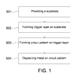
- FIG. 1 shows a flowchart of a method for forming a metal circuit according to an embodiment.
- the method includes steps S01 to S04.
- step S01 a substrate is provided.
- step S02 a trigger layer is formed on the substrate.
- step S03 a circuit pattern is formed on the trigger layer.
- step S04 a metal is deposited on the circuit pattern.
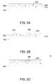
- a substrate 100 is provided, and a first trigger layer 200 is formed on the substrate 100.
- the substrate 100 may be made of a conductive material or a non-conductive material.
- the substrate 100 has a flat surface.
- the first trigger layer 200 may be formed on a substrate 100 having any shape to form a stereoscopic metal circuit structure.
- the first trigger layer 200 is formed by heating and curing a trigger material.
- the trigger material includes an insulating gel 210, and a plurality of trigger particles 220 distributed in the insulating gel 210.
- the insulating gel 210 is a macromolecular material, e.g., epoxy, polyurethane (PU) or cyclic olefin copolymer/polymer (COC/COP), and requires a curing temperature that is lower than a heat-resistant temperature or a glass transition temperature Tg of the substrate 100.
- the glass transition temperatures Tg of the substrate 100 and the insulating gel 210 are both greater than 60°C.
- the viscosity of the liquid trigger material mixed with the trigger particles 220 is lower than 10000 centipoise (cP)
- the cured first trigger layer 200 is smooth and uniform.
- the trigger particles 220 are active particles having a high dielectric constant, such as organometallic particles, a chelation, a semiconductor material having an energy gap greater than or equal to 3 eV, or combinations thereof.
- the trigger material after curing has a dielectric constant between 2 and 6.5.
- the trigger material may further include a pigment 222.
- the pigment 222 may be a common pigment, and includes either an inorganic pigment or an organic pigment.
- the addition of the pigment 222 increases the laser absorption rate of the macromolecular material so that a subsequent laser ablation step (to be described later) can be facilitated.
- the liquid trigger material according to the embodiment is complete after evenly distributing the pigment 222 and the trigger particles 220 in the insulating gel 210.
- the trigger material is sprayed, screen printed or applied to cover a predetermined position for forming the metal circuit layer on the substrate 100. Once the trigger material is heated and becomes cured, the first trigger layer 200 is formed.
- the trigger particles 220 constitute approximately 0.1 to 30 weight percent of the trigger material
- the pigment 222 constitutes approximately 3 to 30 weight percent of the trigger material.
- the trigger particles 220 may be organometallic particles.
- An organometal is a compound containing bonds between a metal and carbon.
- the structure of an organometal is represented as R-M-R' or R-M-X, where M is a metal, e.g., gold, silver, copper, tin, aluminum, nickel, palladium or combinations thereof, R and R' are organic functional groups including an alkyl group, aromatic hydrocarbons group, cycloalkyl group, alkyl halide, heterocycle group or carboxylic acid, and X is a halogen compound or an amine group.
- the organic particles may be lithium 2-thienylcyanocuprate (C 5 H 3 CuLiNS).
- the metal M may be bonded with two or more organic functional groups R or R'.
- the metal M may be bonded with four or six organic functional groups R or R'.
- the multiple organic functional groups R or R' bonded with the metal M may be the same or different.
- the trigger particles 220 may also be a chelation formed from a metal chelated by a chelating agent.
- trigger particles 220 may be formed by ammonium pyrrolidine dithiocarbamate (APDC) that chelates copper, iron, nickel, zinc or combinations thereof, or a chelating agent such as ethylenediaminetetraacetic acid (EDTA), N-N'- bis (carboxymethyl) nitrotriacetate or diethylenetriamine pentaacetic acid (DTPA) that chelates gold, silver, copper, tin, aluminum, nickel, palladium or combinations thereof.
- APDC ammonium pyrrolidine dithiocarbamate
- EDTA ethylenediaminetetraacetic acid
- DTPA diethylenetriamine pentaacetic acid
- the types of chelates and metals adopted are not limited by the disclosure.
- the trigger particles 220 may be a semiconductor material having an energy gap greater than or equal to 3 eV.
- Semiconductor materials having an energy gap greater than or equal to 3 eV include gallium nitride (GaN), zinc sulfide (ZnS), silicon carbide (SiC), zinc oxide (ZnO), titanium dioxide (TiO 2 ) and aluminum gallium nitride (AlGaN).
- Semiconductor materials having an energy gap greater than or equal to 4 eV include aluminum nitride (AlN), aluminum oxide (Al 2 O 3 ), boron nitride (BN), silicon nitride (Si 3 N 4 ) and silicon dioxide (SiO 2 ).
- the trigger particles 220 may be at least one material selected from the group consisting of the above semiconductor materials.
- the first trigger layer 200 formed from a cured mixture of the trigger particles 220 and the insulating gel 210 also has a higher dielectric constant.
- the dielectric constant of the first trigger layer 200 is between 2 and 6.5.
- the metal circuit formed according to the embodiment, without causing signal interference may be applied to a high-frequency circuit of a radio circuit,.
- the thickness and position of formation of the first trigger layer 200 may be adjusted as desired. Instead of covering as a complete layer on the substrate 100 as shown in FIG. 2A , the liquid trigger material may be sprayed or applied to a predetermined region on the substrate 100 to keep the trigger particles 220 concentrated and to reduce the amount of material used. In one embodiment, the thickness of the first trigger layer 200 is between 10 and 100 ⁇ m.
- the LDS technology involves dual materials of a catalyst and plastic particles for injection molding, a colossal amount of catalyst is required for a large-size application, and the catalyst is liable to be unevenly distributed such that the metal circuit cannot be readily formed.
- the injection equipment utilized in the LDS technology has a limitation of approximately 200 ⁇ m, so that the result yielded by the LDS technology is far larger than the range achieved by this embodiment.
- the first trigger layer 200 is ablated by a laser having a first wavelength to form a first circuit pattern 230 according to a metal circuit layer to be formed, such that the first circuit pattern 230 exposes and activates a part of the trigger particles 220.
- the laser may be implemented by a high-energy laser (e.g., a YAG laser).
- the depth, line width and size of the first circuit pattern 230 may be altered based on product requirements by merely changing the energy and irradiation time of the laser. It should be noted that, the first circuit pattern 230 needs to expose and reveal the trigger particles 220 in the trigger layer 200 in order to deposit a metal material in a subsequent process.
- the weight percentage of the trigger particles 220 in the first trigger layer 200 may be adjusted as desired.
- a first circuit pattern 230 having a shallow and narrow formation is sufficient for revealing and exposing the trigger particles 220.
- the first circuit patter 230 is required to have a deeper and wider formation in order to reveal and expose the trigger particles 220.
- the first circuit pattern 230 may be have a line width smaller than or equal to 30 ⁇ m and a depth of 5 to 15 ⁇ m, so that a first metal circuit layer 300 can be provided with the same line width and depth in a subsequent process.
- the line width provided by the embodiment is noticeably reduced (30%).
- a metal material is deposited on the first circuit pattern 230 to form the first metal circuit layer 300, thus successfully forming a metal circuit on the substrate 100.
- the metal material can be deposited by electroless plating.
- the structure shown in FIG. 2B is placed in an electrolyte, and an oxidation reduction reaction happens between to-be-plated metal ions in the electrolyte and the trigger particles 220 exposed on the first circuit pattern 230, such that the to-be-plated metal ions are reduced to a metal and deposited on the first circuit pattern 230.
- the trigger particles 220 are an organometal or a chelation
- the laser severs the covalent bond R-M between the organic functional group and the metal to expose a part of the metal.
- the trigger particles 220 are a semiconductor material having an energy gap of greater than or equal to 3 eV
- the laser energy excites the covalent electrons in the semiconductor material, generates electron hole, so that the semiconductor material can be spontaneously reduced. Therefore, only the trigger particles 220 at the part (i.e., the first circuit pattern 230) on the first trigger layer 200 irradiated by the laser are activated to deposit the metal material thereupon.
- the first wavelength of the laser may be adjusted according to the trigger particles 220 selected, e.g., between 400 to 1200 nm.
- a metal circuit structure 10 includes the substrate 100, the first trigger layer 200 and the first metal circuit layer 300.
- the first trigger layer 200 is disposed on the substrate 100 and includes the first circuit pattern 230.
- the first metal circuit layer 300 is disposed on the first circuit pattern 230, and is electrically insulated from the first metal circuit layer 230 and the substrate 100.
- the composition of the first trigger layer 200 formed by the cured liquid trigger material is the same as that of the trigger material, and so associated details shall be omitted herein.
- the metal circuit structure 10 shown in FIG. 2C has one single metal circuit layer 300, but is not limited thereto.
- the method for forming a metal circuit may form a metal circuit structure having multiple metal circuit layers.
- a metal circuit structure 20 shown in FIG. 3 includes two metal circuit layers, which are a first metal circuit layer 300 and a second metal circuit layer 300'.
- a structural difference of the metal circuit structure 20 from the metal circuit structure 10 in FIG. 2C is that, the metal circuit structure 20 further includes a second trigger layer 200' for the second metal circuit layer 300'.
- the second trigger layer 200' includes a second circuit pattern (not shown), and covers the first trigger layer 200 and the first metal circuit layer 300; the second metal circuit layer 300' is disposed on the second circuit pattern.
- the method for forming the metal circuit structure 20 in FIG. 3 iterates steps S02 to S04.
- the second trigger layer 200' is formed to cover the first trigger layer 200 and the first metal circuit layer 300
- the second circuit pattern is formed on the second trigger layer 200' by the laser having the first wavelength
- the metal material is deposited on the second circuit pattern by electroless plating to form the second metal circuit layer 300'.
- the second trigger layer 200' may be formed by the same trigger material as the first trigger layer 200.
- steps S02 to S04 multiple metal circuit layers can be formed on the substrate 100, so as to form a multi-layer metal circuit structure including multiple metal circuit layers.
- the method of this embodiment is capable of forming more complex circuits applicable to diversified fields.
- the cured first trigger layer 200 and second trigger layer 200' are insulating bodies.
- the maximum depth of the second circuit pattern is designed to be the same as the thickness of the second trigger layer 200 when ablating the second trigger layer 200' by the laser, i.e., the second trigger layer 200' is penetrated through by the ablation.
- an inter-layer connector 310' can be formed at the same time when depositing the second metal circuit layer 300', such that the first metal circuit layer 300 and the second metal circuit layer 300' can be electrically connected, as a metal circuit structure 30 shown in FIG. 4 .
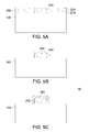
- FIGS. 5A to 5C show detailed steps of a method for forming a metal circuit according to another embodiment.
- the steps in FIGS. 5A to 5C differ from those in FIGS. 2A to 2C in that a trigger material having a different composition is utilized in the method in FIGS. 5A to 5C .
- Corresponding details are the same, and shall be omitted herein.
- a substrate 100 is provided, and a first trigger layer 200 is formed on the substrate 100.
- the first trigger layer 200 is also formed by heating and curing a trigger material, which is made by uniformly mixing insulating gel 210, trigger particles 220 and a photo-initiator (not shown).
- the photo-initiator may be a negative photoresist, e.g., 2-benzyl-2-dimethylamino-1-(4-morpholinophenyl)-1-butanone, 4-acetamidobenzenesulfonyl chloride, or dimethoxy-2-phenylacetophenon (DMPEP).
- the negative photoresist generates bonds when irradiated by beams having a predetermined wavelength, resulting in a reinforced structure.
- the photo-initiator constitutes 0.1 to 10 weight percent of the trigger material.
- the trigger material is sprayed, screen printed or applied onto the substrate 100, and forms the first trigger layer 200 after curing.
- a predetermined position of the first circuit pattern 230 is irradiated by a laser having a predetermined wavelength to cure a part of the photo-initiator of the circuit pattern 230 and to activate a part of the trigger particles 220 at the first circuit pattern 230.
- a laser having the same wavelength may be utilized to simultaneously cure the photo-initiator and activate the trigger particles 220.
- the photo-initiator and the trigger particles 220 may be irradiated twice, with a laser having a second wavelength for curing the photo-initiator and a laser having a first wavelength for activating the trigger particles 220. That is to say, the second wavelength for curing the photo-initiator and the first wavelength for activating the trigger particles 220 may be the same or different.
- the second wavelength for curing the photo-initiator may range between 300 to 500 nm.
- the first trigger layer 200 outside the predetermined position of the first circuit pattern 230 is removed.
- the first trigger layer 200 is immerged in a developing agent.
- the photo-initiator is a negative photoresist
- the part that is not irradiated is dissolved by the developing agent, and the irradiated part is reinforced instead of being removed by the developing agent to leave the first circuit pattern 230.
- a metal material is deposited on the first circuit pattern 230 by electroless plating to generate the first metal circuit layer 300, thus successfully forming a metal circuit on the substrate 100.
- Such a method is capable of forming a metal circuit on a transparent substrate.
- a trigger layer is formed on a substrate by utilizing a specific trigger material, and a metal material is deposited on the trigger layer to form a metal circuit structure.
- the metal circuit structure formed by the method according to the embodiment compared to the conventional LDS technology, has a higher dielectric constant, a smaller thickness and a narrower line width, and can be applied to different substrates to form a metal circuit structure having more than one layer.
Landscapes
- Engineering & Computer Science (AREA)
- Chemical & Material Sciences (AREA)
- Microelectronics & Electronic Packaging (AREA)
- Manufacturing & Machinery (AREA)
- Chemical Kinetics & Catalysis (AREA)
- Organic Chemistry (AREA)
- Materials Engineering (AREA)
- Metallurgy (AREA)
- Mechanical Engineering (AREA)
- General Chemical & Material Sciences (AREA)
- Life Sciences & Earth Sciences (AREA)
- Wood Science & Technology (AREA)
- Health & Medical Sciences (AREA)
- Toxicology (AREA)
- Manufacturing Of Printed Wiring (AREA)
- Chemically Coating (AREA)
- Dispersion Chemistry (AREA)
Abstract
Description
- The disclosure relates in general to a metal circuit structure, a method for forming a metal circuit and a liquid trigger material for forming a metal circuit, and more particularly, to a method for forming a metal circuit on a substrate by electroless plating, a liquid trigger material applied for electroless plating and a metal circuit structure formed using the same.
- To integrate more functions into a single portable electronic device or to miniaturize the size of a portable electronic device, developers and manufacturers strive to reduce the volume of components inside the device. For example, transceiving antennas previously dominated by printed circuit boards are gradually being replaced by a laser direct structuring (LDS) technology that directly electroplates a conductive material on a device casing.
- However, the LDS technology is applicable to only certain plastic substrates, with a limited range of dielectric constants, and thereby is not suitable for high-frequency antennas. Besides, due to injection molding adopted, the LDS technology yields an overall structure that exceeds 2mm. Further, the thickness of a laser-etched conductive circuit needs at least 10-15 µm, and only a single-layer conductive circuit can be formed.
- The disclosure is directed to a metal circuit structure, a method for forming a metal circuit and a liquid trigger material for forming a metal circuit, which are capable of forming a single-layer or multi-layer metal circuit on different types of substrates.
- According to one embodiment, a liquid trigger material that is curable and suitable for forming a metal circuit is provided. The liquid trigger material comprises: an insulating gel comprised of a macromolecular material that is curable; and a plurality of trigger particles comprised of at least one of organometallic particles, a chelation, and a semiconductor material having an energy gap greater than or equal to 3 eV, the trigger particles being activated when irradiated by a laser having a first wavelength; wherein, the trigger particles are distributed in the insulating gel, such that the liquid trigger material has a viscosity of less than 10000 cP. The liquid trigger material, after curing, has a dielectric constant between 2 and 6.5.
- According to another embodiment, a method for forming a metal circuit is provided. The method includes the steps of providing a substrate; forming a first trigger layer on the substrate by applying then curing the liquid trigger material described above; ablating the first trigger layer using a laser having a first wavelength to form a first circuit pattern, such that the first circuit pattern exposes and activates at least a part of the trigger particles; and depositing a metal material on the first circuit pattern by electroless plating to form a first metal circuit layer.
- According to an alternative embodiment, a metal circuit structure is provided. The metal circuit structure includes a substrate; a first trigger layer disposed on the substrate and comprised of a first circuit pattern; and a first metal circuit layer disposed on the first circuit pattern and electrically insulated from the substrate; wherein the first trigger layer has a composition comprised of an insulating gel that is cured; and a plurality of trigger particles comprised of at least one of organometallic particles, a chelation, and a semiconductor material having an energy gap greater than or equal to 3 eV, the plurality of trigger particles being distributed in the insulating gel such that the first trigger layer has a dielectric constant ranging between 2 and 6.5.
-
-
FIG. 1 is a flowchart of a method for forming a metal circuit according to an embodiment; -
FIGS. 2A to 2C are steps of the method for forming a metal circuit inFIG. 1 ; -
FIG. 3 is a metal circuit structure according to an embodiment; -
FIG. 4 is a metal circuit structure according to another embodiment; and -
FIGS. 5A to 5C are steps of a method for forming a metal circuit according to another embodiment. - In the following detailed description, for purposes of explanation, numerous specific details are set forth in order to provide a thorough understanding of the disclosed embodiments. It will be apparent, however, that one or more embodiments may be practiced without these specific details. In other instances, well-known structures and devices are schematically shown in order to simplify the drawing.
-
FIG. 1 shows a flowchart of a method for forming a metal circuit according to an embodiment. As shown inFIG. 1 , the method includes steps S01 to S04. In step S01, a substrate is provided. In step S02, a trigger layer is formed on the substrate. In step S03, a circuit pattern is formed on the trigger layer. In step S04, a metal is deposited on the circuit pattern. With the above method, a single-layer or multi-layer metal circuit can be formed on the substrate. - Details of the steps of the method for forming a metal circuit in
FIG. 1 are given with reference toFIGS. 2A to 2C below. - As shown in
FIG. 2A , asubstrate 100 is provided, and afirst trigger layer 200 is formed on thesubstrate 100. Thesubstrate 100 may be made of a conductive material or a non-conductive material. In the embodiment, thesubstrate 100 has a flat surface. In practice, thefirst trigger layer 200 may be formed on asubstrate 100 having any shape to form a stereoscopic metal circuit structure. Thefirst trigger layer 200 is formed by heating and curing a trigger material. The trigger material includes aninsulating gel 210, and a plurality oftrigger particles 220 distributed in theinsulating gel 210. Theinsulating gel 210 is a macromolecular material, e.g., epoxy, polyurethane (PU) or cyclic olefin copolymer/polymer (COC/COP), and requires a curing temperature that is lower than a heat-resistant temperature or a glass transition temperature Tg of thesubstrate 100. In one embodiment, to perform a subsequent electroless plating process (to be described later), the glass transition temperatures Tg of thesubstrate 100 and theinsulating gel 210 are both greater than 60°C. In one embodiment, when the viscosity of the liquid trigger material mixed with thetrigger particles 220 is lower than 10000 centipoise (cP), the curedfirst trigger layer 200 is smooth and uniform. Thetrigger particles 220 are active particles having a high dielectric constant, such as organometallic particles, a chelation, a semiconductor material having an energy gap greater than or equal to 3 eV, or combinations thereof. In one embodiment, the trigger material after curing has a dielectric constant between 2 and 6.5. The trigger material may further include apigment 222. Thepigment 222 may be a common pigment, and includes either an inorganic pigment or an organic pigment. For example, the inorganic pigment may be titanium dioxide (white) or carbon black (black); and the organic pigment may be an azo pigment (-N = N-), copper phthalocyanine blue (C32H16N8Cu) or phthalocyanine green (C32HCl15N8Cu). The addition of thepigment 222, as an optional element, increases the laser absorption rate of the macromolecular material so that a subsequent laser ablation step (to be described later) can be facilitated. The liquid trigger material according to the embodiment is complete after evenly distributing thepigment 222 and thetrigger particles 220 in theinsulating gel 210. The trigger material is sprayed, screen printed or applied to cover a predetermined position for forming the metal circuit layer on thesubstrate 100. Once the trigger material is heated and becomes cured, thefirst trigger layer 200 is formed. In one embodiment, thetrigger particles 220 constitute approximately 0.1 to 30 weight percent of the trigger material, and thepigment 222 constitutes approximately 3 to 30 weight percent of the trigger material. - As previously stated, the
trigger particles 220 may be organometallic particles. An organometal is a compound containing bonds between a metal and carbon. The structure of an organometal is represented as R-M-R' or R-M-X, where M is a metal, e.g., gold, silver, copper, tin, aluminum, nickel, palladium or combinations thereof, R and R' are organic functional groups including an alkyl group, aromatic hydrocarbons group, cycloalkyl group, alkyl halide, heterocycle group or carboxylic acid, and X is a halogen compound or an amine group. In one embodiment, the organic particles may be lithium 2-thienylcyanocuprate (C5H3CuLiNS). phenylmagnesium chloride, (C6H5ClMg), 4-(tributylstannyl)pyridine (C17H31NSn), ethylaluminum dichloride (C2H5AlCl2) or combinations thereof. It should be noted that, in the structure R-M-R' of an organometal, the metal M may be bonded with two or more organic functional groups R or R'. For example, in one embodiment, the metal M may be bonded with four or six organic functional groups R or R'. Further, the multiple organic functional groups R or R' bonded with the metal M may be the same or different. - The
trigger particles 220 may also be a chelation formed from a metal chelated by a chelating agent. For example, triggerparticles 220 may be formed by ammonium pyrrolidine dithiocarbamate (APDC) that chelates copper, iron, nickel, zinc or combinations thereof, or a chelating agent such as ethylenediaminetetraacetic acid (EDTA), N-N'- bis (carboxymethyl) nitrotriacetate or diethylenetriamine pentaacetic acid (DTPA) that chelates gold, silver, copper, tin, aluminum, nickel, palladium or combinations thereof. The types of chelates and metals adopted are not limited by the disclosure. - The
trigger particles 220 may be a semiconductor material having an energy gap greater than or equal to 3 eV. Semiconductor materials having an energy gap greater than or equal to 3 eV include gallium nitride (GaN), zinc sulfide (ZnS), silicon carbide (SiC), zinc oxide (ZnO), titanium dioxide (TiO2) and aluminum gallium nitride (AlGaN). Semiconductor materials having an energy gap greater than or equal to 4 eV include aluminum nitride (AlN), aluminum oxide (Al2O3), boron nitride (BN), silicon nitride (Si3N4) and silicon dioxide (SiO2). Thetrigger particles 220 may be at least one material selected from the group consisting of the above semiconductor materials. - It should be noted that, when metal ions are surrounded by an organic functional group R or a chelating agent, electrons are prohibited from free movements. That is to say, the three types of
trigger particles 220 above are non-conductive before the subsequent laser ablation step is performed, and have a higher dielectric constant. Thus, thefirst trigger layer 200 formed from a cured mixture of thetrigger particles 220 and the insulatinggel 210 also has a higher dielectric constant. In one embodiment, the dielectric constant of thefirst trigger layer 200 is between 2 and 6.5. Compared to the conventional LDS technology that adopts metal particles as trigger particles for the subsequent electroless plating process, thefirst trigger layer 200 of the embodiment has excellent insulating properties and is thus less prone to electricity leakage. As having a higher dielectric constant, the metal circuit formed according to the embodiment, without causing signal interference, may be applied to a high-frequency circuit of a radio circuit,. - Since the
first trigger layer 200 is formed by curing the liquid trigger material, the thickness and position of formation of thefirst trigger layer 200 may be adjusted as desired. Instead of covering as a complete layer on thesubstrate 100 as shown inFIG. 2A , the liquid trigger material may be sprayed or applied to a predetermined region on thesubstrate 100 to keep thetrigger particles 220 concentrated and to reduce the amount of material used. In one embodiment, the thickness of thefirst trigger layer 200 is between 10 and 100 µm. In contrast, as the LDS technology involves dual materials of a catalyst and plastic particles for injection molding, a colossal amount of catalyst is required for a large-size application, and the catalyst is liable to be unevenly distributed such that the metal circuit cannot be readily formed. Further, the injection equipment utilized in the LDS technology has a limitation of approximately 200 µm, so that the result yielded by the LDS technology is far larger than the range achieved by this embodiment. - Again referring to
FIG. 2B , after forming thefirst trigger layer 200 on thesubstrate 100, thefirst trigger layer 200 is ablated by a laser having a first wavelength to form afirst circuit pattern 230 according to a metal circuit layer to be formed, such that thefirst circuit pattern 230 exposes and activates a part of thetrigger particles 220. In one embodiment, for example, the laser may be implemented by a high-energy laser (e.g., a YAG laser). The depth, line width and size of thefirst circuit pattern 230 may be altered based on product requirements by merely changing the energy and irradiation time of the laser. It should be noted that, thefirst circuit pattern 230 needs to expose and reveal thetrigger particles 220 in thetrigger layer 200 in order to deposit a metal material in a subsequent process. - The weight percentage of the
trigger particles 220 in thefirst trigger layer 200 may be adjusted as desired. When the weight percentage of thetrigger particles 220 to the trigger material is high, afirst circuit pattern 230 having a shallow and narrow formation is sufficient for revealing and exposing thetrigger particles 220. In contrast, when the weight percentage of thetrigger particles 220 to the trigger material is low, thefirst circuit patter 230 is required to have a deeper and wider formation in order to reveal and expose thetrigger particles 220. In one embodiment, when the weight percentage of thetrigger particles 220 to the trigger material is 1 to 2 weight percent, thefirst circuit pattern 230 may be have a line width smaller than or equal to 30 µm and a depth of 5 to 15 µm, so that a firstmetal circuit layer 300 can be provided with the same line width and depth in a subsequent process. Compared to the conventional LDS technology in which the line width of a metal circuit is 80 to 100 µm, the line width provided by the embodiment is noticeably reduced (30%). - As shown in
FIG. 2C , a metal material is deposited on thefirst circuit pattern 230 to form the firstmetal circuit layer 300, thus successfully forming a metal circuit on thesubstrate 100. The metal material can be deposited by electroless plating. The structure shown inFIG. 2B is placed in an electrolyte, and an oxidation reduction reaction happens between to-be-plated metal ions in the electrolyte and thetrigger particles 220 exposed on thefirst circuit pattern 230, such that the to-be-plated metal ions are reduced to a metal and deposited on thefirst circuit pattern 230. When thetrigger particles 220 are an organometal or a chelation, the laser severs the covalent bond R-M between the organic functional group and the metal to expose a part of the metal. When thetrigger particles 220 are a semiconductor material having an energy gap of greater than or equal to 3 eV, the laser energy excites the covalent electrons in the semiconductor material, generates electron hole, so that the semiconductor material can be spontaneously reduced. Therefore, only thetrigger particles 220 at the part (i.e., the first circuit pattern 230) on thefirst trigger layer 200 irradiated by the laser are activated to deposit the metal material thereupon. The first wavelength of the laser may be adjusted according to thetrigger particles 220 selected, e.g., between 400 to 1200 nm. - Thus, referring to
FIG. 2C showing the metal circuit structure formed by the above method, ametal circuit structure 10 includes thesubstrate 100, thefirst trigger layer 200 and the firstmetal circuit layer 300. Thefirst trigger layer 200 is disposed on thesubstrate 100 and includes thefirst circuit pattern 230. The firstmetal circuit layer 300 is disposed on thefirst circuit pattern 230, and is electrically insulated from the firstmetal circuit layer 230 and thesubstrate 100. Further, the composition of thefirst trigger layer 200 formed by the cured liquid trigger material is the same as that of the trigger material, and so associated details shall be omitted herein. - It should be noted that, the
metal circuit structure 10 shown inFIG. 2C has one singlemetal circuit layer 300, but is not limited thereto. The method for forming a metal circuit according to one embodiment may form a metal circuit structure having multiple metal circuit layers. For example, ametal circuit structure 20 shown inFIG. 3 includes two metal circuit layers, which are a firstmetal circuit layer 300 and a second metal circuit layer 300'. A structural difference of themetal circuit structure 20 from themetal circuit structure 10 inFIG. 2C is that, themetal circuit structure 20 further includes a second trigger layer 200' for the second metal circuit layer 300'. The second trigger layer 200' includes a second circuit pattern (not shown), and covers thefirst trigger layer 200 and the firstmetal circuit layer 300; the second metal circuit layer 300' is disposed on the second circuit pattern. - After completing the single-layer
metal circuit structure 10 inFIG. 2C , the method for forming themetal circuit structure 20 inFIG. 3 iterates steps S02 to S04. In step S02 to S04, the second trigger layer 200' is formed to cover thefirst trigger layer 200 and the firstmetal circuit layer 300, the second circuit pattern is formed on the second trigger layer 200' by the laser having the first wavelength, and the metal material is deposited on the second circuit pattern by electroless plating to form the second metal circuit layer 300'. The second trigger layer 200' may be formed by the same trigger material as thefirst trigger layer 200. Similarly, by repeating steps S02 to S04, multiple metal circuit layers can be formed on thesubstrate 100, so as to form a multi-layer metal circuit structure including multiple metal circuit layers. Compared to the conventional LDS technology which is incapable of manufacturing multi-layer circuits, the method of this embodiment is capable of forming more complex circuits applicable to diversified fields. - The cured
first trigger layer 200 and second trigger layer 200' are insulating bodies. Thus, by controlling the depth of the second metal circuit layer 300' in the second trigger layer 200', the second metal circuit layer 300' and the firstmetal circuit layer 300 can be prevented from coming into contact and from shortening. Conversely, to electrically connect the firstmetal circuit layer 300 and the second metal circuit layer 300', the maximum depth of the second circuit pattern is designed to be the same as the thickness of thesecond trigger layer 200 when ablating the second trigger layer 200' by the laser, i.e., the second trigger layer 200' is penetrated through by the ablation. As such, an inter-layer connector 310' can be formed at the same time when depositing the second metal circuit layer 300', such that the firstmetal circuit layer 300 and the second metal circuit layer 300' can be electrically connected, as ametal circuit structure 30 shown inFIG. 4 . -
FIGS. 5A to 5C show detailed steps of a method for forming a metal circuit according to another embodiment. The steps inFIGS. 5A to 5C differ from those inFIGS. 2A to 2C in that a trigger material having a different composition is utilized in the method inFIGS. 5A to 5C . Corresponding details are the same, and shall be omitted herein. - As shown in
FIG. 5A , asubstrate 100 is provided, and afirst trigger layer 200 is formed on thesubstrate 100. Thefirst trigger layer 200 is also formed by heating and curing a trigger material, which is made by uniformly mixing insulatinggel 210,trigger particles 220 and a photo-initiator (not shown). For example, the photo-initiator may be a negative photoresist, e.g., 2-benzyl-2-dimethylamino-1-(4-morpholinophenyl)-1-butanone, 4-acetamidobenzenesulfonyl chloride, or dimethoxy-2-phenylacetophenon (DMPEP). The negative photoresist generates bonds when irradiated by beams having a predetermined wavelength, resulting in a reinforced structure. In one embodiment, for example, the photo-initiator constitutes 0.1 to 10 weight percent of the trigger material. The trigger material is sprayed, screen printed or applied onto thesubstrate 100, and forms thefirst trigger layer 200 after curing. After forming thefirst trigger layer 200, a predetermined position of thefirst circuit pattern 230 is irradiated by a laser having a predetermined wavelength to cure a part of the photo-initiator of thecircuit pattern 230 and to activate a part of thetrigger particles 220 at thefirst circuit pattern 230. Based on different selections of photo-initiators and triggerparticles 220, a laser having the same wavelength may be utilized to simultaneously cure the photo-initiator and activate thetrigger particles 220. Alternatively, the photo-initiator and thetrigger particles 220 may be irradiated twice, with a laser having a second wavelength for curing the photo-initiator and a laser having a first wavelength for activating thetrigger particles 220. That is to say, the second wavelength for curing the photo-initiator and the first wavelength for activating thetrigger particles 220 may be the same or different. For example, the second wavelength for curing the photo-initiator may range between 300 to 500 nm. - As shown in
FIG. 5B , thefirst trigger layer 200 outside the predetermined position of thefirst circuit pattern 230 is removed. For example, thefirst trigger layer 200 is immerged in a developing agent. As the photo-initiator is a negative photoresist, the part that is not irradiated is dissolved by the developing agent, and the irradiated part is reinforced instead of being removed by the developing agent to leave thefirst circuit pattern 230. - As shown in
FIG. 5C , a metal material is deposited on thefirst circuit pattern 230 by electroless plating to generate the firstmetal circuit layer 300, thus successfully forming a metal circuit on thesubstrate 100. Such a method is capable of forming a metal circuit on a transparent substrate. - In the method for forming a metal circuit disclosed by the above embodiment, a trigger layer is formed on a substrate by utilizing a specific trigger material, and a metal material is deposited on the trigger layer to form a metal circuit structure. The metal circuit structure formed by the method according to the embodiment, compared to the conventional LDS technology, has a higher dielectric constant, a smaller thickness and a narrower line width, and can be applied to different substrates to form a metal circuit structure having more than one layer.
- It will be apparent to those skilled in the art that various modifications and variations can be made to the disclosed embodiments. It is intended that the specification and examples be considered as exemplary only, with a true scope of the disclosure being indicated by the following claims and their equivalents.
Claims (16)
- A liquid trigger material that is curable and suitable for forming a metal circuit
characterized in that the liquid trigger material comprise:an insulating gel (210) comprised of a macromolecular material that is curable; anda plurality of trigger particles (220) comprised of at least one of organometallic particles, a chelation, and a semiconductor material having an energy gap greater than or equal to 3 eV, the trigger particles (220) being activated when irradiated by a laser having a first wavelength;wherein, the trigger particles (220) are distributed in the insulating gel (210), such that the liquid trigger material has a viscosity of less than 10000 cP, and the liquid trigger material after curing has a dielectric constant ranging between 2 and 6.5. - The liquid trigger material according to claim 1, wherein the first wavelength ranges between 400 and 1200 nm, and the trigger particles (220) constitute 0.1 to 30 weight percent of the trigger material.
- The liquid trigger material according to any one of claims 1-2, wherein, when the trigger particles (220) are said semiconductor having the energy gap greater than or equal to 3 eV, the trigger particles (220) are gallium nitride (GaN), zinc sulfide (ZnS), silicon carbide (SiC), zinc oxide (ZnO), titanium dioxide (TiO2), aluminum gallium nitride (AlGaN), aluminum nitride (AIN), aluminum oxide (Al2O3), boron nitride (BN), silicon nitride (Si3N4), silicon dioxide (SiO2) or combinations thereof.
- The liquid trigger material according to any one of claims 1-2, wherein, when the trigger particles (220) are said organometallic particles, the trigger particles (220) have a structure that is R-M-R' or R-M-X, where M is a metal, R and R' are an alkyl group, an aromatic hydrocarbon group, a cycloalkyl group, an alkyl halide group, a heterocycle group or a carboxylic acid group, and X is a halogen compound or amine group.
- The liquid trigger material according to any one of claims 1-2, wherein, when the trigger particles (220) are said chelation, the trigger particles (220) are formed from a metal chelated by a chelating agent, and the chelating agent is ammonium pyrrolidine dithiocarbamate (APDC), ethylenediaminetetraacetic acid (EDTA), N-N'- bis (carboxymethyl) nitrotriacetate, diethylenetriamine pentaacetic acid (DTPA) or combinations thereof.
- The liquid trigger material according to any one of claims 1-5, further comprising a photo-initiator that is mixed into the insulating gel, the photo-initiator is curable by a laser having a second wavelength, the photo-initiator constitutes 0.1 to 10 weight percent of the trigger material, and the second wavelength ranges between 300 and 500 nm.
- The liquid trigger material according to any one of claims 1-6, further comprising a pigment (222) that is distributed in the insulating gel and that constitutes 3 to 30 weight percent of the trigger material.
- A method for forming a metal circuit
characterized in that the method comprises following steps:providing a substrate (100);forming a first trigger layer (200) on the substrate (100) by applying then curing the liquid trigger material of any one of claims 1-7;ablating the first trigger layer (200) using a laser having a first wavelength to form a first circuit pattern (230), such that the first circuit pattern (230) exposes and activates at least a part of the trigger particles (220); anddepositing a metal material on the first circuit pattern by electroless plating to form a first metal circuit layer (300). - The method according to claim 8, further comprising:forming a second trigger layer (200') that covers the first trigger layer (200) and the first metal circuit layer (300) by applying then curing a liquid trigger material;forming a second circuit pattern on the second trigger layer (200') using the laser having the first wavelength; anddepositing a metal material on the second circuit pattern by electroless plating to form a second metal circuit layer (300'), such that a plurality of layers of metal circuits are present on the substrate (100).
- The method according to any one of claims 8-9, wherein the liquid trigger material comprises a photo-initiator, and the method further comprises curing the photo-initiator using a laser having a second wavelength; subsequently activating the trigger particles (220) using the laser having the second wavelength, and removing a part of the first trigger layer (200) that is not irradiated using the laser having a second wavelength.
- A metal circuit structure (10), comprising:a substrate (100);a first trigger layer (200) disposed on the substrate (100) and comprised of a first circuit pattern (230); anda first metal circuit layer (300) disposed on the first circuit pattern (230) and electrically insulated from the substrate (100);characterized in that
the first trigger layer (200) has a composition comprised of an insulating gel (210) that is cured; and a plurality of trigger particles (220) comprised of at least one of organometallic particles, a chelation, and a semiconductor material having an energy gap greater than or equal to 3 eV, the plurality of trigger particles (220) being distributed in the insulating gel (210) such that the first trigger layer (200) has a dielectric constant ranging between 2 and 6.5. - The metal circuit structure (10) according to claim 11, further comprising:a second trigger layer (200') including a second circuit pattern and covering the first trigger layer (200) and the first metal circuit layer (300); anda second metal circuit layer (300') disposed on the second circuit pattern;wherein, the second trigger layer (200') is made of a material that is the same as that of the first trigger layer (200).
- The metal circuit structure (10) according to claim 12, wherein the second trigger layer (200') has a thickness, and wherein the second circuit pattern has a maximum depth that is the same as the thickness of the second trigger layer (200'), such that an interlayer connector is formed between the first trigger layer (200) and the second trigger layer (200').
- The metal circuit structure (10) according to any one of claims 11-13, wherein the first trigger layer (200) has a thickness ranging between 10 and 100 µm, and the first metal circuit layer (300) has a line width that is smaller than or equal to 30 µm.
- The metal circuit structure (10) according to any one of claims 11-14, wherein, when the trigger particles (220) are said semiconductor having the energy gap greater than or equal to 3 eV, the trigger particles (220) are gallium nitride (GaN), zinc sulfide (ZnS), silicon carbide (SiC), zinc oxide (ZnO), titanium dioxide (TiO2), aluminum gallium nitride (AlGaN), aluminum nitride (AIN), aluminum oxide (Al2O3), boron nitride (BN), silicon nitride (Si3N4), silicon dioxide (SiO2) or combinations thereof.
- The metal circuit structure according to claim 11, wherein, when the trigger particles are said organometallic particles, the trigger particles have a structure that is R-M-R' or R-M-X, where M is a metal, R and R' are an alkyl group, an aromatic hydrocarbon group, a cycloalkyl group, an alkyl halide group, a heterocycle group or a carboxylic acid group, and X is a halogen compound or amine group.
Applications Claiming Priority (1)
| Application Number | Priority Date | Filing Date | Title |
|---|---|---|---|
| TW102139840A TWI561132B (en) | 2013-11-01 | 2013-11-01 | Method for forming metal circuit, liquid trigger material for forming metal circuit and metal circuit structure |
Publications (1)
| Publication Number | Publication Date |
|---|---|
| EP2869309A1 true EP2869309A1 (en) | 2015-05-06 |
Family
ID=51211598
Family Applications (1)
| Application Number | Title | Priority Date | Filing Date |
|---|---|---|---|
| EP20140177426 Withdrawn EP2869309A1 (en) | 2013-11-01 | 2014-07-17 | Method for forming metal circuit, liquid trigger material for forming metal circuit and metal circuit structure |
Country Status (4)
| Country | Link |
|---|---|
| US (2) | US9499911B2 (en) |
| EP (1) | EP2869309A1 (en) |
| CN (1) | CN104616720B (en) |
| TW (1) | TWI561132B (en) |
Families Citing this family (11)
| Publication number | Priority date | Publication date | Assignee | Title |
|---|---|---|---|---|
| EP3268985B1 (en) * | 2015-03-09 | 2021-05-19 | Intel Corporation | Selective metallization of an integrated circuit (ic) substrate |
| TWI550525B (en) * | 2015-05-22 | 2016-09-21 | 南茂科技股份有限公司 | Wiring pattern forming method, fingerprint sensing circuit board and manufacturing method thereof |
| CN106548973A (en) * | 2015-09-17 | 2017-03-29 | 中芯长电半导体(江阴)有限公司 | Fan-out-type wafer-level packaging method |
| CN105161433A (en) * | 2015-09-28 | 2015-12-16 | 中芯长电半导体(江阴)有限公司 | Fan-out type wafer grade packaging method |
| TWI563886B (en) | 2015-10-28 | 2016-12-21 | Ind Tech Res Inst | Insulating colloidal material and multilayer circuit structure |
| TWI574595B (en) | 2015-10-28 | 2017-03-11 | 財團法人工業技術研究院 | Manufacturing method for multilayer wiring and multilayer wiring structure |
| TWI584526B (en) | 2015-12-04 | 2017-05-21 | 財團法人工業技術研究院 | Laminated antenna structure |
| WO2018217188A1 (en) * | 2017-05-23 | 2018-11-29 | Intel Corporation | High density package substrate formed with dielectric bi-layer |
| WO2019070387A2 (en) * | 2017-09-15 | 2019-04-11 | Swimmersive Co. | Systems and methods for underwater coaching systems |
| CN108909343B (en) * | 2018-06-08 | 2019-06-07 | 北京梦之墨科技有限公司 | A kind of intelligent graphic is drawn and preparation method thereof |
| CN111805091A (en) * | 2020-06-09 | 2020-10-23 | 深圳市信维通信股份有限公司 | LAP laser etching process |
Citations (4)
| Publication number | Priority date | Publication date | Assignee | Title |
|---|---|---|---|---|
| WO2012150736A1 (en) * | 2011-05-03 | 2012-11-08 | 주식회사 디지아이 | Composition for laser direct structuring and laser direct structuring method using same |
| EP2581469A1 (en) * | 2011-10-10 | 2013-04-17 | Enthone, Inc. | Aqueous activator solution and process for electroless copper deposition on laser-direct structured substrates |
| EP2590217A2 (en) * | 2011-11-01 | 2013-05-08 | Flextronics Ap, Llc | Stacked packages using laser direct structuring |
| US20130203897A1 (en) * | 2010-02-03 | 2013-08-08 | Abb Research Ltd | Electrical insulation system |
Family Cites Families (34)
| Publication number | Priority date | Publication date | Assignee | Title |
|---|---|---|---|---|
| US3836709A (en) * | 1972-04-12 | 1974-09-17 | Grace W R & Co | Process and apparatus for preparing printing plates using a photocured image |
| US6100007A (en) * | 1998-04-06 | 2000-08-08 | Ciba Specialty Chemicals Corp. | Liquid radiation-curable composition especially for producing cured articles by stereolithography having high heat deflection temperatures |
| ES2345031T3 (en) * | 2000-02-08 | 2010-09-14 | Huntsman Advanced Materials (Switzerland) Gmbh | RADIATION CURABLE LIQUID COMPOSITION, ESPECIALLY FOR STEREOLITHOGRAPHY. |
| JP2001313445A (en) | 2000-05-01 | 2001-11-09 | Mitsubishi Gas Chem Co Inc | High relative permittivity printed wiring board |
| EP1209959A3 (en) | 2000-11-27 | 2004-03-10 | Matsushita Electric Works, Ltd. | Multilayer circuit board and method of manufacturing the same |
| DE10132092A1 (en) * | 2001-07-05 | 2003-01-23 | Lpkf Laser & Electronics Ag | Track structures and processes for their manufacture |
| JP4010202B2 (en) | 2002-07-29 | 2007-11-21 | 凸版印刷株式会社 | Multilayer circuit board manufacturing method |
| DE10344512A1 (en) * | 2003-09-24 | 2005-04-28 | Mitsubishi Polyester Film Gmbh | Single-layer, oriented, electromagnetic radiation-structurable thermoplastic polyester film for producing selectively metallized films |
| WO2006030720A1 (en) * | 2004-09-13 | 2006-03-23 | Fujifilm Corporation | Anti-reflection film, polarizing plate, and liquid crystal display device |
| TW200628981A (en) * | 2004-09-29 | 2006-08-16 | Sumitomo Bakelite Co | Semiconductor device |
| DE102006017630A1 (en) * | 2006-04-12 | 2007-10-18 | Lpkf Laser & Electronics Ag | Method for producing a printed conductor structure and a printed conductor structure produced in this way |
| US7815475B2 (en) | 2007-12-21 | 2010-10-19 | Molex Incorporated | Three-dimensional plated support frame |
| US8309640B2 (en) * | 2008-05-23 | 2012-11-13 | Sabic Innovative Plastics Ip B.V. | High dielectric constant laser direct structuring materials |
| CN101640972B (en) | 2008-07-28 | 2011-09-07 | 欣兴电子股份有限公司 | Circuit board structure |
| TWI394506B (en) | 2008-10-13 | 2013-04-21 | Unimicron Technology Corp | Multilayer three-dimensional circuit structure and manufacturing method thereof |
| CN101902884B (en) * | 2009-05-26 | 2012-11-07 | 欣兴电子股份有限公司 | Method of forming composite circuit board structure |
| TWM373574U (en) | 2009-09-23 | 2010-02-01 | Molex Inc | Modular antenna device |
| US8759433B2 (en) * | 2009-12-21 | 2014-06-24 | Mitsubishi Chemical Europe Gmbh | Aromatic polycarbonate composition |
| TWI399143B (en) * | 2009-12-30 | 2013-06-11 | Unimicron Technology Corp | Circuit board and process for fabricating the same |
| TWI456830B (en) | 2010-07-26 | 2014-10-11 | Wistron Neweb Corp | Method for forming antenna structure |
| TWI423750B (en) | 2010-09-24 | 2014-01-11 | 光宏精密股份有限公司 | Non-conductive carrier forming circuit structure manufacturing method |
| CN103261301B (en) * | 2010-10-25 | 2016-08-17 | 沙特基础全球技术有限公司 | The electroless plating performance of the improvement of laser direct structuring materials |
| DE102011000138A1 (en) | 2011-01-14 | 2012-07-19 | Lpkf Laser & Electronics Ag | Method for the selective metallization of a substrate and a circuit carrier produced by this method |
| TWI424875B (en) | 2011-03-30 | 2014-02-01 | 英濟股份有限公司 | Laser direct molding material and manufacturing method thereof |
| CN103765215A (en) * | 2011-06-07 | 2014-04-30 | 生命科技公司 | Fluorogenic semiconductor nanocrystals |
| TWM421670U (en) | 2011-08-29 | 2012-01-21 | Paragon Technologies Co Ltd | 3D circuit structure |
| KR20140091029A (en) * | 2011-10-31 | 2014-07-18 | 티코나 엘엘씨 | Thermoplastic composition for use in forming a laser direct structured substrate |
| TWM433058U (en) | 2011-12-13 | 2012-07-01 | 3D Circuit Taiwan | Conductive vias of three-dimensional curved surface and metal layer structure |
| TWM430013U (en) | 2012-01-05 | 2012-05-21 | Joytech Co Ltd | Antenna structure for mobile device |
| TWI425888B (en) * | 2012-01-19 | 2014-02-01 | Kuang Hong Prec Co Ltd | Circuit substrate structure and manufacturing method thereof |
| TWM448053U (en) | 2012-10-25 | 2013-03-01 | 3D Circuit | Sensor module |
| TWM447458U (en) | 2012-10-25 | 2013-02-21 | 3D Circuit Taiwan | Three-dimensional bulb lamp of light emitting element |
| US20140220844A1 (en) * | 2013-02-06 | 2014-08-07 | Isola Usa Corp. | Prepregs and Laminates Having Homogeneous Dielectric Properties |
| TWI577257B (en) * | 2014-12-24 | 2017-04-01 | 綠點高新科技股份有限公司 | Method of forming conductive lines on an insulating surface of a substrate |
-
2013
- 2013-11-01 TW TW102139840A patent/TWI561132B/en active
- 2013-11-22 CN CN201310595165.3A patent/CN104616720B/en active Active
-
2014
- 2014-07-03 US US14/323,248 patent/US9499911B2/en active Active
- 2014-07-17 EP EP20140177426 patent/EP2869309A1/en not_active Withdrawn
-
2016
- 2016-10-11 US US15/290,668 patent/US9683292B2/en active Active
Patent Citations (4)
| Publication number | Priority date | Publication date | Assignee | Title |
|---|---|---|---|---|
| US20130203897A1 (en) * | 2010-02-03 | 2013-08-08 | Abb Research Ltd | Electrical insulation system |
| WO2012150736A1 (en) * | 2011-05-03 | 2012-11-08 | 주식회사 디지아이 | Composition for laser direct structuring and laser direct structuring method using same |
| EP2581469A1 (en) * | 2011-10-10 | 2013-04-17 | Enthone, Inc. | Aqueous activator solution and process for electroless copper deposition on laser-direct structured substrates |
| EP2590217A2 (en) * | 2011-11-01 | 2013-05-08 | Flextronics Ap, Llc | Stacked packages using laser direct structuring |
Non-Patent Citations (1)
| Title |
|---|
| DATABASE WPI Week 201276, Derwent World Patents Index; AN 2012-P63570, XP002737176 * |
Also Published As
| Publication number | Publication date |
|---|---|
| US9683292B2 (en) | 2017-06-20 |
| CN104616720A (en) | 2015-05-13 |
| US9499911B2 (en) | 2016-11-22 |
| US20170029953A1 (en) | 2017-02-02 |
| TWI561132B (en) | 2016-12-01 |
| CN104616720B (en) | 2018-05-04 |
| TW201519724A (en) | 2015-05-16 |
| US20150122533A1 (en) | 2015-05-07 |
Similar Documents
| Publication | Publication Date | Title |
|---|---|---|
| US9683292B2 (en) | Metal circuit structure | |
| KR102247655B1 (en) | Semiconductor device and method of manufacture | |
| KR101464322B1 (en) | Electromagnetic wave shielding structure and method for fabricating the same | |
| TW587992B (en) | Wiring substrate | |
| TW507507B (en) | Liquid thermosetting resin composition, printed wiring boards and process for their production | |
| CN1732565B (en) | Method for performing substrate imprinting with thermosetting resin varnish and product formed therefrom | |
| CN109119380B (en) | Electronic circuit package using composite magnetic encapsulant | |
| JPWO2010087336A1 (en) | Semiconductor chip mounting method, semiconductor device obtained by using the method, semiconductor chip connection method, three-dimensional structure provided with wiring on the surface, and manufacturing method thereof | |
| CN110169210B (en) | Integrated Circuit Wafer Integration Using Catalytic Laminates or Adhesives | |
| CN109564899A (en) | The manufacturing method of supporting substrate, the laminated body with supporting substrate and semiconductor element package for mounting substrate | |
| US9468095B1 (en) | Manufacturing method of multilayer wiring and multilayer wiring structure | |
| WO2017164174A1 (en) | Electromagnetic shielding film | |
| JP6425062B2 (en) | Insulating resin sheet, and circuit board and semiconductor package using the same | |
| JP2010056179A (en) | Conductor forming sheet, and method of manufacturing wiring board using conductor forming sheet | |
| CN106658936A (en) | Insulating colloid material and multilayer circuit structure | |
| KR102716421B1 (en) | Adhesive composition for insulating film, insulating film sheet and method for manufacturing printed wiring board | |
| JP2015090954A (en) | Flexible printed wiring board and method for manufacturing the same | |
| TW201609853A (en) | Epoxy-resin-containing varnish, epoxy-resin-composition-containing varnish, prepreg, resin sheet, laminate board, printed circuit board, semiconductor device | |
| He et al. | Laser Direct Structuring of Semiconductor Liquid Encapsulants for Active Mold Packaging | |
| TW202106136A (en) | Circuit board and method for making the same | |
| TW201218873A (en) | Wiring substrate, power structural body, method of manufacturing the wiring substrate and method of manufacturing the power structural body | |
| KR20170067540A (en) | Printed circuit board and method of manufacturing the same | |
| JP2006086233A (en) | Multilayer interconnection board and manufacturing method thereof | |
| KR101870191B1 (en) | Manufacturing method of circuit board | |
| TWI259044B (en) | Printed circuit board and method for making the same |
Legal Events
| Date | Code | Title | Description |
|---|---|---|---|
| PUAI | Public reference made under article 153(3) epc to a published international application that has entered the european phase |
Free format text: ORIGINAL CODE: 0009012 |
|
| 17P | Request for examination filed |
Effective date: 20140717 |
|
| AK | Designated contracting states |
Kind code of ref document: A1 Designated state(s): AL AT BE BG CH CY CZ DE DK EE ES FI FR GB GR HR HU IE IS IT LI LT LU LV MC MK MT NL NO PL PT RO RS SE SI SK SM TR |
|
| AX | Request for extension of the european patent |
Extension state: BA ME |
|
| R17P | Request for examination filed (corrected) |
Effective date: 20150611 |
|
| RBV | Designated contracting states (corrected) |
Designated state(s): AL AT BE BG CH CY CZ DE DK EE ES FI FR GB GR HR HU IE IS IT LI LT LU LV MC MK MT NL NO PL PT RO RS SE SI SK SM TR |
|
| STAA | Information on the status of an ep patent application or granted ep patent |
Free format text: STATUS: EXAMINATION IS IN PROGRESS |
|
| 17Q | First examination report despatched |
Effective date: 20171011 |
|
| STAA | Information on the status of an ep patent application or granted ep patent |
Free format text: STATUS: THE APPLICATION IS DEEMED TO BE WITHDRAWN |
|
| 18D | Application deemed to be withdrawn |
Effective date: 20221220 |