EP2863440A1 - Silicon carbide semiconductor device and method for producing same - Google Patents
Silicon carbide semiconductor device and method for producing same Download PDFInfo
- Publication number
- EP2863440A1 EP2863440A1 EP13804906.9A EP13804906A EP2863440A1 EP 2863440 A1 EP2863440 A1 EP 2863440A1 EP 13804906 A EP13804906 A EP 13804906A EP 2863440 A1 EP2863440 A1 EP 2863440A1
- Authority
- EP
- European Patent Office
- Prior art keywords
- region
- trench
- layer
- conductivity type
- silicon carbide
- Prior art date
- Legal status (The legal status is an assumption and is not a legal conclusion. Google has not performed a legal analysis and makes no representation as to the accuracy of the status listed.)
- Granted
Links
- 239000004065 semiconductor Substances 0.000 title claims abstract description 102
- HBMJWWWQQXIZIP-UHFFFAOYSA-N silicon carbide Chemical compound [Si+]#[C-] HBMJWWWQQXIZIP-UHFFFAOYSA-N 0.000 title claims description 97
- 229910010271 silicon carbide Inorganic materials 0.000 title claims description 97
- 238000004519 manufacturing process Methods 0.000 title claims description 26
- 238000009413 insulation Methods 0.000 claims abstract description 48
- 239000012535 impurity Substances 0.000 claims description 94
- 230000002093 peripheral effect Effects 0.000 claims description 48
- 239000000758 substrate Substances 0.000 claims description 36
- 238000005530 etching Methods 0.000 claims description 11
- 238000000034 method Methods 0.000 claims description 6
- 230000004888 barrier function Effects 0.000 claims description 3
- 230000005684 electric field Effects 0.000 abstract description 14
- 230000009467 reduction Effects 0.000 abstract description 5
- 239000010410 layer Substances 0.000 description 145
- 239000011229 interlayer Substances 0.000 description 11
- 239000000463 material Substances 0.000 description 8
- 238000010586 diagram Methods 0.000 description 6
- 238000005468 ion implantation Methods 0.000 description 6
- 239000002344 surface layer Substances 0.000 description 5
- 230000015556 catabolic process Effects 0.000 description 4
- 229910052739 hydrogen Inorganic materials 0.000 description 4
- 239000001257 hydrogen Substances 0.000 description 4
- UFHFLCQGNIYNRP-UHFFFAOYSA-N Hydrogen Chemical compound [H][H] UFHFLCQGNIYNRP-UHFFFAOYSA-N 0.000 description 3
- 229910052751 metal Inorganic materials 0.000 description 3
- 239000002184 metal Substances 0.000 description 3
- 230000004048 modification Effects 0.000 description 3
- 238000012986 modification Methods 0.000 description 3
- 230000003647 oxidation Effects 0.000 description 3
- 238000007254 oxidation reaction Methods 0.000 description 3
- 238000000206 photolithography Methods 0.000 description 3
- 238000001020 plasma etching Methods 0.000 description 3
- 239000007772 electrode material Substances 0.000 description 2
- 238000000059 patterning Methods 0.000 description 2
- 238000005498 polishing Methods 0.000 description 2
- 229910021420 polycrystalline silicon Inorganic materials 0.000 description 2
- 229920005591 polysilicon Polymers 0.000 description 2
- 230000015572 biosynthetic process Effects 0.000 description 1
- 238000010276 construction Methods 0.000 description 1
- 230000006837 decompression Effects 0.000 description 1
- 230000003247 decreasing effect Effects 0.000 description 1
- 238000000151 deposition Methods 0.000 description 1
- 238000009826 distribution Methods 0.000 description 1
- 239000002019 doping agent Substances 0.000 description 1
- 239000007789 gas Substances 0.000 description 1
- 238000000227 grinding Methods 0.000 description 1
- 238000010438 heat treatment Methods 0.000 description 1
- 150000002431 hydrogen Chemical class 0.000 description 1
- 150000002739 metals Chemical class 0.000 description 1
- 150000004767 nitrides Chemical class 0.000 description 1
- 230000001590 oxidative effect Effects 0.000 description 1
- 239000000126 substance Substances 0.000 description 1
Images


Classifications
-
- H—ELECTRICITY
- H01—ELECTRIC ELEMENTS
- H01L—SEMICONDUCTOR DEVICES NOT COVERED BY CLASS H10
- H01L29/00—Semiconductor devices specially adapted for rectifying, amplifying, oscillating or switching and having potential barriers; Capacitors or resistors having potential barriers, e.g. a PN-junction depletion layer or carrier concentration layer; Details of semiconductor bodies or of electrodes thereof ; Multistep manufacturing processes therefor
- H01L29/02—Semiconductor bodies ; Multistep manufacturing processes therefor
- H01L29/12—Semiconductor bodies ; Multistep manufacturing processes therefor characterised by the materials of which they are formed
- H01L29/16—Semiconductor bodies ; Multistep manufacturing processes therefor characterised by the materials of which they are formed including, apart from doping materials or other impurities, only elements of Group IV of the Periodic Table
-
- H—ELECTRICITY
- H01—ELECTRIC ELEMENTS
- H01L—SEMICONDUCTOR DEVICES NOT COVERED BY CLASS H10
- H01L21/00—Processes or apparatus adapted for the manufacture or treatment of semiconductor or solid state devices or of parts thereof
- H01L21/02—Manufacture or treatment of semiconductor devices or of parts thereof
- H01L21/04—Manufacture or treatment of semiconductor devices or of parts thereof the devices having potential barriers, e.g. a PN junction, depletion layer or carrier concentration layer
- H01L21/0445—Manufacture or treatment of semiconductor devices or of parts thereof the devices having potential barriers, e.g. a PN junction, depletion layer or carrier concentration layer the devices having semiconductor bodies comprising crystalline silicon carbide
- H01L21/0455—Making n or p doped regions or layers, e.g. using diffusion
- H01L21/046—Making n or p doped regions or layers, e.g. using diffusion using ion implantation
-
- H—ELECTRICITY
- H01—ELECTRIC ELEMENTS
- H01L—SEMICONDUCTOR DEVICES NOT COVERED BY CLASS H10
- H01L21/00—Processes or apparatus adapted for the manufacture or treatment of semiconductor or solid state devices or of parts thereof
- H01L21/02—Manufacture or treatment of semiconductor devices or of parts thereof
- H01L21/04—Manufacture or treatment of semiconductor devices or of parts thereof the devices having potential barriers, e.g. a PN junction, depletion layer or carrier concentration layer
- H01L21/0445—Manufacture or treatment of semiconductor devices or of parts thereof the devices having potential barriers, e.g. a PN junction, depletion layer or carrier concentration layer the devices having semiconductor bodies comprising crystalline silicon carbide
- H01L21/0475—Changing the shape of the semiconductor body, e.g. forming recesses
-
- H—ELECTRICITY
- H01—ELECTRIC ELEMENTS
- H01L—SEMICONDUCTOR DEVICES NOT COVERED BY CLASS H10
- H01L21/00—Processes or apparatus adapted for the manufacture or treatment of semiconductor or solid state devices or of parts thereof
- H01L21/02—Manufacture or treatment of semiconductor devices or of parts thereof
- H01L21/04—Manufacture or treatment of semiconductor devices or of parts thereof the devices having potential barriers, e.g. a PN junction, depletion layer or carrier concentration layer
- H01L21/18—Manufacture or treatment of semiconductor devices or of parts thereof the devices having potential barriers, e.g. a PN junction, depletion layer or carrier concentration layer the devices having semiconductor bodies comprising elements of Group IV of the Periodic Table or AIIIBV compounds with or without impurities, e.g. doping materials
- H01L21/30—Treatment of semiconductor bodies using processes or apparatus not provided for in groups H01L21/20 - H01L21/26
- H01L21/302—Treatment of semiconductor bodies using processes or apparatus not provided for in groups H01L21/20 - H01L21/26 to change their surface-physical characteristics or shape, e.g. etching, polishing, cutting
- H01L21/306—Chemical or electrical treatment, e.g. electrolytic etching
- H01L21/30604—Chemical etching
-
- H—ELECTRICITY
- H01—ELECTRIC ELEMENTS
- H01L—SEMICONDUCTOR DEVICES NOT COVERED BY CLASS H10
- H01L21/00—Processes or apparatus adapted for the manufacture or treatment of semiconductor or solid state devices or of parts thereof
- H01L21/02—Manufacture or treatment of semiconductor devices or of parts thereof
- H01L21/04—Manufacture or treatment of semiconductor devices or of parts thereof the devices having potential barriers, e.g. a PN junction, depletion layer or carrier concentration layer
- H01L21/18—Manufacture or treatment of semiconductor devices or of parts thereof the devices having potential barriers, e.g. a PN junction, depletion layer or carrier concentration layer the devices having semiconductor bodies comprising elements of Group IV of the Periodic Table or AIIIBV compounds with or without impurities, e.g. doping materials
- H01L21/30—Treatment of semiconductor bodies using processes or apparatus not provided for in groups H01L21/20 - H01L21/26
- H01L21/302—Treatment of semiconductor bodies using processes or apparatus not provided for in groups H01L21/20 - H01L21/26 to change their surface-physical characteristics or shape, e.g. etching, polishing, cutting
- H01L21/306—Chemical or electrical treatment, e.g. electrolytic etching
- H01L21/308—Chemical or electrical treatment, e.g. electrolytic etching using masks
-
- H—ELECTRICITY
- H01—ELECTRIC ELEMENTS
- H01L—SEMICONDUCTOR DEVICES NOT COVERED BY CLASS H10
- H01L21/00—Processes or apparatus adapted for the manufacture or treatment of semiconductor or solid state devices or of parts thereof
- H01L21/70—Manufacture or treatment of devices consisting of a plurality of solid state components formed in or on a common substrate or of parts thereof; Manufacture of integrated circuit devices or of parts thereof
- H01L21/71—Manufacture of specific parts of devices defined in group H01L21/70
- H01L21/76—Making of isolation regions between components
- H01L21/761—PN junctions
-
- H—ELECTRICITY
- H01—ELECTRIC ELEMENTS
- H01L—SEMICONDUCTOR DEVICES NOT COVERED BY CLASS H10
- H01L21/00—Processes or apparatus adapted for the manufacture or treatment of semiconductor or solid state devices or of parts thereof
- H01L21/70—Manufacture or treatment of devices consisting of a plurality of solid state components formed in or on a common substrate or of parts thereof; Manufacture of integrated circuit devices or of parts thereof
- H01L21/77—Manufacture or treatment of devices consisting of a plurality of solid state components or integrated circuits formed in, or on, a common substrate
- H01L21/78—Manufacture or treatment of devices consisting of a plurality of solid state components or integrated circuits formed in, or on, a common substrate with subsequent division of the substrate into plural individual devices
- H01L21/82—Manufacture or treatment of devices consisting of a plurality of solid state components or integrated circuits formed in, or on, a common substrate with subsequent division of the substrate into plural individual devices to produce devices, e.g. integrated circuits, each consisting of a plurality of components
- H01L21/8213—Manufacture or treatment of devices consisting of a plurality of solid state components or integrated circuits formed in, or on, a common substrate with subsequent division of the substrate into plural individual devices to produce devices, e.g. integrated circuits, each consisting of a plurality of components the substrate being a semiconductor, using SiC technology
-
- H—ELECTRICITY
- H01—ELECTRIC ELEMENTS
- H01L—SEMICONDUCTOR DEVICES NOT COVERED BY CLASS H10
- H01L29/00—Semiconductor devices specially adapted for rectifying, amplifying, oscillating or switching and having potential barriers; Capacitors or resistors having potential barriers, e.g. a PN-junction depletion layer or carrier concentration layer; Details of semiconductor bodies or of electrodes thereof ; Multistep manufacturing processes therefor
- H01L29/02—Semiconductor bodies ; Multistep manufacturing processes therefor
- H01L29/06—Semiconductor bodies ; Multistep manufacturing processes therefor characterised by their shape; characterised by the shapes, relative sizes, or dispositions of the semiconductor regions ; characterised by the concentration or distribution of impurities within semiconductor regions
- H01L29/0603—Semiconductor bodies ; Multistep manufacturing processes therefor characterised by their shape; characterised by the shapes, relative sizes, or dispositions of the semiconductor regions ; characterised by the concentration or distribution of impurities within semiconductor regions characterised by particular constructional design considerations, e.g. for preventing surface leakage, for controlling electric field concentration or for internal isolations regions
- H01L29/0607—Semiconductor bodies ; Multistep manufacturing processes therefor characterised by their shape; characterised by the shapes, relative sizes, or dispositions of the semiconductor regions ; characterised by the concentration or distribution of impurities within semiconductor regions characterised by particular constructional design considerations, e.g. for preventing surface leakage, for controlling electric field concentration or for internal isolations regions for preventing surface leakage or controlling electric field concentration
- H01L29/0611—Semiconductor bodies ; Multistep manufacturing processes therefor characterised by their shape; characterised by the shapes, relative sizes, or dispositions of the semiconductor regions ; characterised by the concentration or distribution of impurities within semiconductor regions characterised by particular constructional design considerations, e.g. for preventing surface leakage, for controlling electric field concentration or for internal isolations regions for preventing surface leakage or controlling electric field concentration for increasing or controlling the breakdown voltage of reverse biased devices
- H01L29/0615—Semiconductor bodies ; Multistep manufacturing processes therefor characterised by their shape; characterised by the shapes, relative sizes, or dispositions of the semiconductor regions ; characterised by the concentration or distribution of impurities within semiconductor regions characterised by particular constructional design considerations, e.g. for preventing surface leakage, for controlling electric field concentration or for internal isolations regions for preventing surface leakage or controlling electric field concentration for increasing or controlling the breakdown voltage of reverse biased devices by the doping profile or the shape or the arrangement of the PN junction, or with supplementary regions, e.g. junction termination extension [JTE]
- H01L29/063—Reduced surface field [RESURF] pn-junction structures
- H01L29/0634—Multiple reduced surface field (multi-RESURF) structures, e.g. double RESURF, charge compensation, cool, superjunction (SJ), 3D-RESURF, composite buffer (CB) structures
-
- H—ELECTRICITY
- H01—ELECTRIC ELEMENTS
- H01L—SEMICONDUCTOR DEVICES NOT COVERED BY CLASS H10
- H01L29/00—Semiconductor devices specially adapted for rectifying, amplifying, oscillating or switching and having potential barriers; Capacitors or resistors having potential barriers, e.g. a PN-junction depletion layer or carrier concentration layer; Details of semiconductor bodies or of electrodes thereof ; Multistep manufacturing processes therefor
- H01L29/02—Semiconductor bodies ; Multistep manufacturing processes therefor
- H01L29/06—Semiconductor bodies ; Multistep manufacturing processes therefor characterised by their shape; characterised by the shapes, relative sizes, or dispositions of the semiconductor regions ; characterised by the concentration or distribution of impurities within semiconductor regions
- H01L29/0657—Semiconductor bodies ; Multistep manufacturing processes therefor characterised by their shape; characterised by the shapes, relative sizes, or dispositions of the semiconductor regions ; characterised by the concentration or distribution of impurities within semiconductor regions characterised by the shape of the body
- H01L29/0661—Semiconductor bodies ; Multistep manufacturing processes therefor characterised by their shape; characterised by the shapes, relative sizes, or dispositions of the semiconductor regions ; characterised by the concentration or distribution of impurities within semiconductor regions characterised by the shape of the body specially adapted for altering the breakdown voltage by removing semiconductor material at, or in the neighbourhood of, a reverse biased junction, e.g. by bevelling, moat etching, depletion etching
-
- H—ELECTRICITY
- H01—ELECTRIC ELEMENTS
- H01L—SEMICONDUCTOR DEVICES NOT COVERED BY CLASS H10
- H01L29/00—Semiconductor devices specially adapted for rectifying, amplifying, oscillating or switching and having potential barriers; Capacitors or resistors having potential barriers, e.g. a PN-junction depletion layer or carrier concentration layer; Details of semiconductor bodies or of electrodes thereof ; Multistep manufacturing processes therefor
- H01L29/02—Semiconductor bodies ; Multistep manufacturing processes therefor
- H01L29/06—Semiconductor bodies ; Multistep manufacturing processes therefor characterised by their shape; characterised by the shapes, relative sizes, or dispositions of the semiconductor regions ; characterised by the concentration or distribution of impurities within semiconductor regions
- H01L29/0684—Semiconductor bodies ; Multistep manufacturing processes therefor characterised by their shape; characterised by the shapes, relative sizes, or dispositions of the semiconductor regions ; characterised by the concentration or distribution of impurities within semiconductor regions characterised by the shape, relative sizes or dispositions of the semiconductor regions or junctions between the regions
- H01L29/0692—Surface layout
- H01L29/0696—Surface layout of cellular field-effect devices, e.g. multicellular DMOS transistors or IGBTs
-
- H—ELECTRICITY
- H01—ELECTRIC ELEMENTS
- H01L—SEMICONDUCTOR DEVICES NOT COVERED BY CLASS H10
- H01L29/00—Semiconductor devices specially adapted for rectifying, amplifying, oscillating or switching and having potential barriers; Capacitors or resistors having potential barriers, e.g. a PN-junction depletion layer or carrier concentration layer; Details of semiconductor bodies or of electrodes thereof ; Multistep manufacturing processes therefor
- H01L29/02—Semiconductor bodies ; Multistep manufacturing processes therefor
- H01L29/06—Semiconductor bodies ; Multistep manufacturing processes therefor characterised by their shape; characterised by the shapes, relative sizes, or dispositions of the semiconductor regions ; characterised by the concentration or distribution of impurities within semiconductor regions
- H01L29/10—Semiconductor bodies ; Multistep manufacturing processes therefor characterised by their shape; characterised by the shapes, relative sizes, or dispositions of the semiconductor regions ; characterised by the concentration or distribution of impurities within semiconductor regions with semiconductor regions connected to an electrode not carrying current to be rectified, amplified or switched and such electrode being part of a semiconductor device which comprises three or more electrodes
- H01L29/1095—Body region, i.e. base region, of DMOS transistors or IGBTs
-
- H—ELECTRICITY
- H01—ELECTRIC ELEMENTS
- H01L—SEMICONDUCTOR DEVICES NOT COVERED BY CLASS H10
- H01L29/00—Semiconductor devices specially adapted for rectifying, amplifying, oscillating or switching and having potential barriers; Capacitors or resistors having potential barriers, e.g. a PN-junction depletion layer or carrier concentration layer; Details of semiconductor bodies or of electrodes thereof ; Multistep manufacturing processes therefor
- H01L29/02—Semiconductor bodies ; Multistep manufacturing processes therefor
- H01L29/12—Semiconductor bodies ; Multistep manufacturing processes therefor characterised by the materials of which they are formed
- H01L29/15—Structures with periodic or quasi periodic potential variation, e.g. multiple quantum wells, superlattices
- H01L29/157—Doping structures, e.g. doping superlattices, nipi superlattices
-
- H—ELECTRICITY
- H01—ELECTRIC ELEMENTS
- H01L—SEMICONDUCTOR DEVICES NOT COVERED BY CLASS H10
- H01L29/00—Semiconductor devices specially adapted for rectifying, amplifying, oscillating or switching and having potential barriers; Capacitors or resistors having potential barriers, e.g. a PN-junction depletion layer or carrier concentration layer; Details of semiconductor bodies or of electrodes thereof ; Multistep manufacturing processes therefor
- H01L29/02—Semiconductor bodies ; Multistep manufacturing processes therefor
- H01L29/12—Semiconductor bodies ; Multistep manufacturing processes therefor characterised by the materials of which they are formed
- H01L29/15—Structures with periodic or quasi periodic potential variation, e.g. multiple quantum wells, superlattices
- H01L29/158—Structures without potential periodicity in a direction perpendicular to a major surface of the substrate, i.e. vertical direction, e.g. lateral superlattices, lateral surface superlattices [LSS]
-
- H—ELECTRICITY
- H01—ELECTRIC ELEMENTS
- H01L—SEMICONDUCTOR DEVICES NOT COVERED BY CLASS H10
- H01L29/00—Semiconductor devices specially adapted for rectifying, amplifying, oscillating or switching and having potential barriers; Capacitors or resistors having potential barriers, e.g. a PN-junction depletion layer or carrier concentration layer; Details of semiconductor bodies or of electrodes thereof ; Multistep manufacturing processes therefor
- H01L29/02—Semiconductor bodies ; Multistep manufacturing processes therefor
- H01L29/12—Semiconductor bodies ; Multistep manufacturing processes therefor characterised by the materials of which they are formed
- H01L29/16—Semiconductor bodies ; Multistep manufacturing processes therefor characterised by the materials of which they are formed including, apart from doping materials or other impurities, only elements of Group IV of the Periodic Table
- H01L29/1608—Silicon carbide
-
- H—ELECTRICITY
- H01—ELECTRIC ELEMENTS
- H01L—SEMICONDUCTOR DEVICES NOT COVERED BY CLASS H10
- H01L29/00—Semiconductor devices specially adapted for rectifying, amplifying, oscillating or switching and having potential barriers; Capacitors or resistors having potential barriers, e.g. a PN-junction depletion layer or carrier concentration layer; Details of semiconductor bodies or of electrodes thereof ; Multistep manufacturing processes therefor
- H01L29/40—Electrodes ; Multistep manufacturing processes therefor
- H01L29/41—Electrodes ; Multistep manufacturing processes therefor characterised by their shape, relative sizes or dispositions
- H01L29/423—Electrodes ; Multistep manufacturing processes therefor characterised by their shape, relative sizes or dispositions not carrying the current to be rectified, amplified or switched
- H01L29/42312—Gate electrodes for field effect devices
- H01L29/42316—Gate electrodes for field effect devices for field-effect transistors
- H01L29/4232—Gate electrodes for field effect devices for field-effect transistors with insulated gate
- H01L29/42356—Disposition, e.g. buried gate electrode
- H01L29/4236—Disposition, e.g. buried gate electrode within a trench, e.g. trench gate electrode, groove gate electrode
-
- H—ELECTRICITY
- H01—ELECTRIC ELEMENTS
- H01L—SEMICONDUCTOR DEVICES NOT COVERED BY CLASS H10
- H01L29/00—Semiconductor devices specially adapted for rectifying, amplifying, oscillating or switching and having potential barriers; Capacitors or resistors having potential barriers, e.g. a PN-junction depletion layer or carrier concentration layer; Details of semiconductor bodies or of electrodes thereof ; Multistep manufacturing processes therefor
- H01L29/66—Types of semiconductor device ; Multistep manufacturing processes therefor
- H01L29/66007—Multistep manufacturing processes
- H01L29/66053—Multistep manufacturing processes of devices having a semiconductor body comprising crystalline silicon carbide
- H01L29/66068—Multistep manufacturing processes of devices having a semiconductor body comprising crystalline silicon carbide the devices being controllable only by the electric current supplied or the electric potential applied, to an electrode which does not carry the current to be rectified, amplified or switched, e.g. three-terminal devices
-
- H—ELECTRICITY
- H01—ELECTRIC ELEMENTS
- H01L—SEMICONDUCTOR DEVICES NOT COVERED BY CLASS H10
- H01L29/00—Semiconductor devices specially adapted for rectifying, amplifying, oscillating or switching and having potential barriers; Capacitors or resistors having potential barriers, e.g. a PN-junction depletion layer or carrier concentration layer; Details of semiconductor bodies or of electrodes thereof ; Multistep manufacturing processes therefor
- H01L29/66—Types of semiconductor device ; Multistep manufacturing processes therefor
- H01L29/66007—Multistep manufacturing processes
- H01L29/66075—Multistep manufacturing processes of devices having semiconductor bodies comprising group 14 or group 13/15 materials
- H01L29/66227—Multistep manufacturing processes of devices having semiconductor bodies comprising group 14 or group 13/15 materials the devices being controllable only by the electric current supplied or the electric potential applied, to an electrode which does not carry the current to be rectified, amplified or switched, e.g. three-terminal devices
- H01L29/66409—Unipolar field-effect transistors
- H01L29/66477—Unipolar field-effect transistors with an insulated gate, i.e. MISFET
- H01L29/66674—DMOS transistors, i.e. MISFETs with a channel accommodating body or base region adjoining a drain drift region
- H01L29/66712—Vertical DMOS transistors, i.e. VDMOS transistors
- H01L29/66727—Vertical DMOS transistors, i.e. VDMOS transistors with a step of recessing the source electrode
-
- H—ELECTRICITY
- H01—ELECTRIC ELEMENTS
- H01L—SEMICONDUCTOR DEVICES NOT COVERED BY CLASS H10
- H01L29/00—Semiconductor devices specially adapted for rectifying, amplifying, oscillating or switching and having potential barriers; Capacitors or resistors having potential barriers, e.g. a PN-junction depletion layer or carrier concentration layer; Details of semiconductor bodies or of electrodes thereof ; Multistep manufacturing processes therefor
- H01L29/66—Types of semiconductor device ; Multistep manufacturing processes therefor
- H01L29/66007—Multistep manufacturing processes
- H01L29/66075—Multistep manufacturing processes of devices having semiconductor bodies comprising group 14 or group 13/15 materials
- H01L29/66227—Multistep manufacturing processes of devices having semiconductor bodies comprising group 14 or group 13/15 materials the devices being controllable only by the electric current supplied or the electric potential applied, to an electrode which does not carry the current to be rectified, amplified or switched, e.g. three-terminal devices
- H01L29/66409—Unipolar field-effect transistors
- H01L29/66477—Unipolar field-effect transistors with an insulated gate, i.e. MISFET
- H01L29/66674—DMOS transistors, i.e. MISFETs with a channel accommodating body or base region adjoining a drain drift region
- H01L29/66712—Vertical DMOS transistors, i.e. VDMOS transistors
- H01L29/66734—Vertical DMOS transistors, i.e. VDMOS transistors with a step of recessing the gate electrode, e.g. to form a trench gate electrode
-
- H—ELECTRICITY
- H01—ELECTRIC ELEMENTS
- H01L—SEMICONDUCTOR DEVICES NOT COVERED BY CLASS H10
- H01L29/00—Semiconductor devices specially adapted for rectifying, amplifying, oscillating or switching and having potential barriers; Capacitors or resistors having potential barriers, e.g. a PN-junction depletion layer or carrier concentration layer; Details of semiconductor bodies or of electrodes thereof ; Multistep manufacturing processes therefor
- H01L29/66—Types of semiconductor device ; Multistep manufacturing processes therefor
- H01L29/68—Types of semiconductor device ; Multistep manufacturing processes therefor controllable by only the electric current supplied, or only the electric potential applied, to an electrode which does not carry the current to be rectified, amplified or switched
- H01L29/76—Unipolar devices, e.g. field effect transistors
- H01L29/772—Field effect transistors
- H01L29/78—Field effect transistors with field effect produced by an insulated gate
- H01L29/7801—DMOS transistors, i.e. MISFETs with a channel accommodating body or base region adjoining a drain drift region
- H01L29/7802—Vertical DMOS transistors, i.e. VDMOS transistors
- H01L29/7803—Vertical DMOS transistors, i.e. VDMOS transistors structurally associated with at least one other device
- H01L29/7806—Vertical DMOS transistors, i.e. VDMOS transistors structurally associated with at least one other device the other device being a Schottky barrier diode
-
- H—ELECTRICITY
- H01—ELECTRIC ELEMENTS
- H01L—SEMICONDUCTOR DEVICES NOT COVERED BY CLASS H10
- H01L29/00—Semiconductor devices specially adapted for rectifying, amplifying, oscillating or switching and having potential barriers; Capacitors or resistors having potential barriers, e.g. a PN-junction depletion layer or carrier concentration layer; Details of semiconductor bodies or of electrodes thereof ; Multistep manufacturing processes therefor
- H01L29/66—Types of semiconductor device ; Multistep manufacturing processes therefor
- H01L29/68—Types of semiconductor device ; Multistep manufacturing processes therefor controllable by only the electric current supplied, or only the electric potential applied, to an electrode which does not carry the current to be rectified, amplified or switched
- H01L29/76—Unipolar devices, e.g. field effect transistors
- H01L29/772—Field effect transistors
- H01L29/78—Field effect transistors with field effect produced by an insulated gate
- H01L29/7801—DMOS transistors, i.e. MISFETs with a channel accommodating body or base region adjoining a drain drift region
- H01L29/7802—Vertical DMOS transistors, i.e. VDMOS transistors
- H01L29/7811—Vertical DMOS transistors, i.e. VDMOS transistors with an edge termination structure
-
- H—ELECTRICITY
- H01—ELECTRIC ELEMENTS
- H01L—SEMICONDUCTOR DEVICES NOT COVERED BY CLASS H10
- H01L29/00—Semiconductor devices specially adapted for rectifying, amplifying, oscillating or switching and having potential barriers; Capacitors or resistors having potential barriers, e.g. a PN-junction depletion layer or carrier concentration layer; Details of semiconductor bodies or of electrodes thereof ; Multistep manufacturing processes therefor
- H01L29/66—Types of semiconductor device ; Multistep manufacturing processes therefor
- H01L29/68—Types of semiconductor device ; Multistep manufacturing processes therefor controllable by only the electric current supplied, or only the electric potential applied, to an electrode which does not carry the current to be rectified, amplified or switched
- H01L29/76—Unipolar devices, e.g. field effect transistors
- H01L29/772—Field effect transistors
- H01L29/78—Field effect transistors with field effect produced by an insulated gate
- H01L29/7801—DMOS transistors, i.e. MISFETs with a channel accommodating body or base region adjoining a drain drift region
- H01L29/7802—Vertical DMOS transistors, i.e. VDMOS transistors
- H01L29/7813—Vertical DMOS transistors, i.e. VDMOS transistors with trench gate electrode, e.g. UMOS transistors
-
- H—ELECTRICITY
- H01—ELECTRIC ELEMENTS
- H01L—SEMICONDUCTOR DEVICES NOT COVERED BY CLASS H10
- H01L29/00—Semiconductor devices specially adapted for rectifying, amplifying, oscillating or switching and having potential barriers; Capacitors or resistors having potential barriers, e.g. a PN-junction depletion layer or carrier concentration layer; Details of semiconductor bodies or of electrodes thereof ; Multistep manufacturing processes therefor
- H01L29/66—Types of semiconductor device ; Multistep manufacturing processes therefor
- H01L29/86—Types of semiconductor device ; Multistep manufacturing processes therefor controllable only by variation of the electric current supplied, or only the electric potential applied, to one or more of the electrodes carrying the current to be rectified, amplified, oscillated or switched
- H01L29/861—Diodes
- H01L29/872—Schottky diodes
-
- H—ELECTRICITY
- H01—ELECTRIC ELEMENTS
- H01L—SEMICONDUCTOR DEVICES NOT COVERED BY CLASS H10
- H01L29/00—Semiconductor devices specially adapted for rectifying, amplifying, oscillating or switching and having potential barriers; Capacitors or resistors having potential barriers, e.g. a PN-junction depletion layer or carrier concentration layer; Details of semiconductor bodies or of electrodes thereof ; Multistep manufacturing processes therefor
- H01L29/02—Semiconductor bodies ; Multistep manufacturing processes therefor
- H01L29/06—Semiconductor bodies ; Multistep manufacturing processes therefor characterised by their shape; characterised by the shapes, relative sizes, or dispositions of the semiconductor regions ; characterised by the concentration or distribution of impurities within semiconductor regions
- H01L29/0603—Semiconductor bodies ; Multistep manufacturing processes therefor characterised by their shape; characterised by the shapes, relative sizes, or dispositions of the semiconductor regions ; characterised by the concentration or distribution of impurities within semiconductor regions characterised by particular constructional design considerations, e.g. for preventing surface leakage, for controlling electric field concentration or for internal isolations regions
- H01L29/0607—Semiconductor bodies ; Multistep manufacturing processes therefor characterised by their shape; characterised by the shapes, relative sizes, or dispositions of the semiconductor regions ; characterised by the concentration or distribution of impurities within semiconductor regions characterised by particular constructional design considerations, e.g. for preventing surface leakage, for controlling electric field concentration or for internal isolations regions for preventing surface leakage or controlling electric field concentration
- H01L29/0611—Semiconductor bodies ; Multistep manufacturing processes therefor characterised by their shape; characterised by the shapes, relative sizes, or dispositions of the semiconductor regions ; characterised by the concentration or distribution of impurities within semiconductor regions characterised by particular constructional design considerations, e.g. for preventing surface leakage, for controlling electric field concentration or for internal isolations regions for preventing surface leakage or controlling electric field concentration for increasing or controlling the breakdown voltage of reverse biased devices
- H01L29/0615—Semiconductor bodies ; Multistep manufacturing processes therefor characterised by their shape; characterised by the shapes, relative sizes, or dispositions of the semiconductor regions ; characterised by the concentration or distribution of impurities within semiconductor regions characterised by particular constructional design considerations, e.g. for preventing surface leakage, for controlling electric field concentration or for internal isolations regions for preventing surface leakage or controlling electric field concentration for increasing or controlling the breakdown voltage of reverse biased devices by the doping profile or the shape or the arrangement of the PN junction, or with supplementary regions, e.g. junction termination extension [JTE]
- H01L29/063—Reduced surface field [RESURF] pn-junction structures
-
- H—ELECTRICITY
- H01—ELECTRIC ELEMENTS
- H01L—SEMICONDUCTOR DEVICES NOT COVERED BY CLASS H10
- H01L29/00—Semiconductor devices specially adapted for rectifying, amplifying, oscillating or switching and having potential barriers; Capacitors or resistors having potential barriers, e.g. a PN-junction depletion layer or carrier concentration layer; Details of semiconductor bodies or of electrodes thereof ; Multistep manufacturing processes therefor
- H01L29/02—Semiconductor bodies ; Multistep manufacturing processes therefor
- H01L29/06—Semiconductor bodies ; Multistep manufacturing processes therefor characterised by their shape; characterised by the shapes, relative sizes, or dispositions of the semiconductor regions ; characterised by the concentration or distribution of impurities within semiconductor regions
- H01L29/08—Semiconductor bodies ; Multistep manufacturing processes therefor characterised by their shape; characterised by the shapes, relative sizes, or dispositions of the semiconductor regions ; characterised by the concentration or distribution of impurities within semiconductor regions with semiconductor regions connected to an electrode carrying current to be rectified, amplified or switched and such electrode being part of a semiconductor device which comprises three or more electrodes
- H01L29/0843—Source or drain regions of field-effect devices
- H01L29/0847—Source or drain regions of field-effect devices of field-effect transistors with insulated gate
- H01L29/0852—Source or drain regions of field-effect devices of field-effect transistors with insulated gate of DMOS transistors
- H01L29/0873—Drain regions
- H01L29/0878—Impurity concentration or distribution
-
- H—ELECTRICITY
- H01—ELECTRIC ELEMENTS
- H01L—SEMICONDUCTOR DEVICES NOT COVERED BY CLASS H10
- H01L29/00—Semiconductor devices specially adapted for rectifying, amplifying, oscillating or switching and having potential barriers; Capacitors or resistors having potential barriers, e.g. a PN-junction depletion layer or carrier concentration layer; Details of semiconductor bodies or of electrodes thereof ; Multistep manufacturing processes therefor
- H01L29/40—Electrodes ; Multistep manufacturing processes therefor
- H01L29/41—Electrodes ; Multistep manufacturing processes therefor characterised by their shape, relative sizes or dispositions
- H01L29/417—Electrodes ; Multistep manufacturing processes therefor characterised by their shape, relative sizes or dispositions carrying the current to be rectified, amplified or switched
- H01L29/41725—Source or drain electrodes for field effect devices
- H01L29/41766—Source or drain electrodes for field effect devices with at least part of the source or drain electrode having contact below the semiconductor surface, e.g. the source or drain electrode formed at least partially in a groove or with inclusions of conductor inside the semiconductor
-
- H—ELECTRICITY
- H01—ELECTRIC ELEMENTS
- H01L—SEMICONDUCTOR DEVICES NOT COVERED BY CLASS H10
- H01L29/00—Semiconductor devices specially adapted for rectifying, amplifying, oscillating or switching and having potential barriers; Capacitors or resistors having potential barriers, e.g. a PN-junction depletion layer or carrier concentration layer; Details of semiconductor bodies or of electrodes thereof ; Multistep manufacturing processes therefor
- H01L29/66—Types of semiconductor device ; Multistep manufacturing processes therefor
- H01L29/86—Types of semiconductor device ; Multistep manufacturing processes therefor controllable only by variation of the electric current supplied, or only the electric potential applied, to one or more of the electrodes carrying the current to be rectified, amplified, oscillated or switched
- H01L29/861—Diodes
-
- Y—GENERAL TAGGING OF NEW TECHNOLOGICAL DEVELOPMENTS; GENERAL TAGGING OF CROSS-SECTIONAL TECHNOLOGIES SPANNING OVER SEVERAL SECTIONS OF THE IPC; TECHNICAL SUBJECTS COVERED BY FORMER USPC CROSS-REFERENCE ART COLLECTIONS [XRACs] AND DIGESTS
- Y10—TECHNICAL SUBJECTS COVERED BY FORMER USPC
- Y10S—TECHNICAL SUBJECTS COVERED BY FORMER USPC CROSS-REFERENCE ART COLLECTIONS [XRACs] AND DIGESTS
- Y10S438/00—Semiconductor device manufacturing: process
- Y10S438/974—Substrate surface preparation
Definitions
- the present disclosure relates to a silicon carbide (hereinafter referred to as SiC) semiconductor device having a switching element with a trench gate structure, and a method for producing the same.
- SiC silicon carbide
- a patent literature 1 has proposed an SiC semiconductor device that aims to restrict breakage of a gate insulation film in a MOSFET with a trench gate structure and to improve surge withstand (avalanche resistance) of the element.
- a p + type deep layer is provided to a position lower than the bottom surface of the trench, between trench gate structures, and is further deepened at a middle of a cell region.
- a patent literature 2 has conventionally proposed a Si semiconductor device that enables reduction of an on-state resistance in a MOSFET with a trench gate structure.
- the Si semiconductor device has a super junction (hereinafter referred to as the SJ) structure in which n type columns for forming n type drift layers and p type columns are alternately arranged, under the trench gate structure. Since the SJ structure is provided in this manner, when the MOSFET is turned off, an electric field is evenly applied in the SJ to reduce the concentration of electric field. When the MOSFET is turned on, since a current path passing through the SJ structure is formed, the on-state resistance can be reduced.
- the SJ structure employed to the Si semiconductor device can also be employed to the SiC semiconductor device.
- a breakdown electric field intensity of the SiC is greatly higher than that of the Si. Therefore, the intensity of electric field applied to the gate insulation film, when the element is turned off, is high, resulting in breakage of the gate insulation film.
- the present disclosure is made in view of the foregoing issues, and it is an object of the present disclosure to provide an SiC semiconductor device and a method for producing the SiC semiconductor device, which is capable of realizing both of reduction of the on-state resistance and restriction of breakage of the gate insulation film.
- an SiC semiconductor device has a trench gate structure including a gate insulation film and a gate electrode formed within a first trench that extends from a surface of a source region to a position deeper than a base region.
- a second conductivity type region including a second conductivity type first low concentration region and a second conductivity type first high concentration region are formed within a second trench that is deeper than the first trench.
- the first low concentration region has a second conductivity type impurity concentration being relatively low.
- the high concentration region is formed on a surface of the first low concentration region, and has a second conductivity type impurity concentration being relatively higher than that of the first low concentration region.
- the first high concentration region provides a deep layer as being formed deeper than the first low concentration region.
- the SiC semiconductor device has a super junction structure including alternately arranged P and N columns which are provided by the first low concentration region and a portion of the drift layer opposed to the first low concentration region, as a structure of electrically connecting the base region to a source electrode through the source region and the second conductivity type region.
- the SiC semiconductor device has the structure provided with the second conductivity type region including the first low concentration region and the first high concentration region filled in the second trench.
- a second conductivity type column can be provided by the first low concentration region, and the deep layer can be provided by the first high concentration region.
- the SiC semiconductor device can realize both of the reduction of the on-state resistance and the restriction of the breakage of the gate insulation film.
- a region where a semiconductor switching element is formed is referred to as a cell region, and the SiC semiconductor device has an outer peripheral withstand voltage structure in an outer peripheral region surrounding a periphery of the cell region.
- the outer peripheral withstand voltage structure is an impurity embedded layer having a second conductivity type second low concentration region disposed in a third trench.
- the second low concentration region has a second conductivity type impurity concentration being equal to that of the first low concentration region.
- the third trench is formed at a part of the drift layer exposed in a recessed portion of the outer peripheral region, the recessed portion being formed by removing the source region and the base region. The third trench extends from the surface of the drift layer.
- the impurity embedded layer having the similar structure to the second conductivity type region of the cell region is provided, and this impurity embedded layer is filled in the third trench. Therefore, the impurity embedded layer can achieve a function of a guard ring. Further, since this impurity embedded layer can be formed simultaneously with the second conductivity region of the cell region, these production steps can be shared, and thus a production process can be simplified.
- a method for producing an SiC semiconductor device with a semiconductor switching element includes the steps of: preparing a semiconductor substrate in which a drift layer is formed on a main surface of a silicon carbide substrate, a base region is formed on the drift layer, and a source region is further formed on the base region; forming a second trench by performing etching using a mask having an opening at a position corresponding to a region of the semiconductor substrate where the second trench is to be formed; epitaxially growing, in the second trench, a second conductivity type first layer having a second conductivity type impurity concentration being relatively low and a second conductivity type second layer having a second conductivity type impurity concentration being higher than that of the first layer; and partially removing the first layer and the second layer to expose the source region, thereby providing a first low concentration region and a first high concentration region by the first layer and the second layer remaining in the second trench.
- the first low concentration region and the first high concentration region are provided by filling the first layer and the second layer having different impurity concentrations in the same second trench. Therefore, a production process can be simplified, as compared with a case where the first low concentration region for providing the second conductivity type column and the first high concentration region for providing the deep layer are separately formed by independent steps.
- a region where the semiconductor switching element is formed is referred to as a cell region.
- a step of forming the third trench in the outer peripheral region is performed simultaneously with the step of forming the second trench.
- a step of forming the first layer and the second layer in the third trench is performed simultaneously with the step of forming the first layer and the second layer in the second trench.
- a step of forming the impurity embedded region is performed to form the second conductivity type second low concentration region having the second conductivity type impurity concentration equal to that of the first low concentration region by the first layer remaining in the third trench, and to form the second conductivity type second high impurity region having the second conductivity type impurity concentration being higher than that of the second low concentration region and being deeper than the first trench by the second layer.
- the outer peripheral withstand voltage structure provided in the outer peripheral region can be made of the impurity embedded region, and the step of forming the second low concentration region and the second high concentration region providing the impurity embedded region can be shared with the step of forming the first low concentration region and the first high concentration region providing the second conductivity region in the cell region. Therefore, the production process can be simplified.
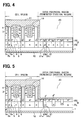
- An SiC semiconductor device shown in Fig. 1 has a structure that includes a cell region in which a semiconductor element is formed, and an outer peripheral region (terminated structure region) in which an outer peripheral withstand voltage structure surrounding the cell region is provided.
- the semiconductor element the MOSFET with the inversion type trench gate structure is provided.
- the SiC semiconductor device is formed using a semiconductor substrate in which an n- type drift layer 2, a p type base region 3, and an n + type source region 4, which are made of SiC, are subsequently epitaxially grown on a main surface of an n + type substrate 1 made of SiC.
- the n + type substrate 1 has an n type impurity concentration of 1.0 x 10 19 /cm 3 , for example, and a thickness of approximately 300 ⁇ m.
- a lower layer portion 2a and an upper layer portion 2b have different n type impurity concentrations.
- the lower layer portion 2a has, for example, the n type impurity concentration of 1.5 to 6.0 x 10 16 /cm 3 , and the thickness of 6.0 ⁇ m.
- the upper layer portion 2b has, for example, the n type impurity concentration of 0.5 to 2.0 x 10 16 /cm 3 , which is lower than that of the lower layer portion 2a, and the thickness of 2.0 ⁇ m.
- the lower layer portion 2a is a portion forming n type columns, and the impurity concentration and the width thereof are determined considering charge balance with p type columns, which will be described later.
- the p type base region 3 has, for example, a p type impurity concentration of 1.5 to 6.0 x 10 16 /cm 3 , and the thickness of approximately 0.5 ⁇ m.
- the n + type source region 4 is formed such that an n type impurity concentration at a surface layer portion thereof is, for example, 2.5 x 10 18 to 1.0 x 10 19 /cm 3 , and has the thickness of approximately 0.5 ⁇ m.
- the p type base region 3 and the n + type source region 4 remain on a side adjacent to the main surface of the semiconductor substrate.
- a p type region 5 is formed to pass through the n + type source region 4 and the p type base region 3 and to reach the n type drift layer 2.
- the p type region 5 is formed to be filled in a trench 5a that is formed to reach the n + type substrate 1.
- the p type region 5 includes two regions 5b, 5c having different p type impurity concentrations.
- the p type region 5 is provided by the low concentration region 5b and the high concentration region 5c.
- the low concentration region 5b is formed on an inner wall surface of the trench 5a, that is, on a bottom surface and side surfaces of the trench 5a.
- the high concentration region 5c has the p type impurity concentration higher than that of the low impurity concentration region 5b.
- the low concentration region 5b is a portion providing a p type column.
- the low concentration region 5b has the p type impurity concentration of 4.15 x 10 16 to 1.65 x 10 17 cm 3 , the width of 0.8 ⁇ m, and the thickness of 8 ⁇ m.
- the p type column is provided by a portion of the low concentration region 5b formed on the bottom surface of the trench 5a, and the thickness of this portion is substantially equal to the thickness of the lower layer portion 2a.
- the width of the low concentration region 5b (that is, the width of the trench 5a) and the p type impurity concentration of the low concentration region 5b are determined considering charge balance with the n type column.
- the high concentration region 5c is a portion providing a p + type deep layer.
- the high concentration region 5c is formed such that the bottom of the high concentration region 5c is located at a position deeper than the bottom of a trench 6 that forms a trench gate structure, which will be described later.
- the high concentration region 5c is formed such that body brake preferentially occurs at the bottom thereof.
- the p type impurity concentration and the width of the high concentration region 5c are determined to restrict complete depletion at the time of body break.
- the p type impurity concentration of the high concentration region 5c is 2.5 x 10 18 to 1.0 x 10 19 /cm 3
- the depth of the high concentration region 5c is 3 ⁇ m.
- n type impurity concentration of the upper layer portion 2b of the n type drift layer 2 is set to 1.0 x 10 16 /cm 3 , and it is assumed that drain voltage of 1200 V is applied at the time of turning off.
- drain voltage of 1200 V is applied at the time of turning off.
- the p type impurity concentration and the width of the high concentration region 5c have the above-described values, a region that is not depleted remains even when reaching the breakdown electric field intensity. For this reason, a breakdown current can be effectively drawn.
- the p type region 5 configured as described above has a layout including a rectangular portion with rounded corners surrounding an outer edge of the cell region and a plurality of line-shaped portions each defining a longitudinal direction in one direction and being arranged in a stripe pattern inside of the rectangular portion, as shown in Fig. 1 .
- the trench 6 is formed to pass through the p type base region 3 and the n + type source region 4 and to reach the n type drift layer 2.
- the trench 6 has the width of 0.8 ⁇ m and the depth of 2.0 ⁇ m, for example.
- the p type base region 3 and the n + type source region 4 are arranged to adjoin the side surface of the trench 6.
- the trench 6 has a line-shaped layout in which a width direction corresponds to a right and left direction on the paper of Fig. 2 , a longitudinal direction corresponds to a direction perpendicular to the plane surface of Fig. 2 , and a depth direction corresponds to the up and down direction on the plane surface of Fig. 2 .
- a plurality of the trenches 6 are arranged parallel to each other at an equal interval into a stripe pattern.
- Each of the line-shaped portions of the p type region 5 is arranged in between the trenches 6.
- the side surface of each of the trenches 6 and the p type region 5 are spaced from each other by a predetermined distance.
- a channel is formed in a portion of the p type base region 3 contacting with the side surface of the trench 6, thereby to allow an electric current to flow.
- the end of the p type region 5 is projected by a distance a relative to the end of each trench 6.
- the distance a is greater than the thickness of the lower layer portion 2a of the n type drift layer 2.
- the distance a is greater than a distance between the lower surface of the high concentration region 5c and a lower surface of the n type drift layer 2.
- the end of each trench 6 is located more to inside than the end of the high concentration region 5c.
- an inner wall surface of the trench 6 is covered with a gate insulation film 8.
- the gate insulation film 8 is, for example, provided by a thermal oxide film formed by thermally oxidizing the inner wall surface of the trench 6, for example.
- the thickness of the gate insulation film 8 on the side surface and the bottom of the trench 6 is approximately 75 nm.
- the corners of the bottom and the ends of the gate insulation film 8 are edged.
- the corners of the bottom and the ends of the gate insulation film 8 may have rounded shapes by subjecting the trench 6 to a rounding treatment beforehand. In such a case, the gate insulation film 8 can entirely have a uniform thickness, and it is less likely that the thickness of the gate insulation film 8 will be reduced at the corner portions of the trench 6.
- a gate electrode 9 is formed on the surface of the gate insulation film 8 to fill the trench 6.
- a source electrode 11 and a gate wiring are formed on the surfaces of the n + type source region 4 and the p type region 5 and the surface of the gate electrode 9 through an interlayer insulation film 10.
- the source electrode 11 and the gate wiring are made of plural metals (for example, Ni and Al), in such a manner that at least a portion contacting with the n type SiC (in particular, the n + type source region 4) is made of a metal that can make an ohmic contact with the n type SiC, and at least a portion contacting with the p type SiC (in particular the p type region 5) is made of a metal that can make an ohmic contact with the p type SiC.
- the source electrode 11 and the gate wiring are electrically insulated as being formed on the interlayer insulation film 10. Via contact holes formed in the interlayer insulation film 10, the source electrode 11 is electrically in contact with the p type base region 3 through the n + type source region 4 and the p type region 5, and the gate wiring is electrically in contact with the gate electrode 9.
- a drain electrode 12 is formed on the rear side of the n + type substrate 1 to be electrically connected to the n + type substrate 1.
- the MOSFET with the n-channel type, inversion type trench gate structure is formed.
- the cell region is provided as the MOSFETs are arranged between the p type regions 5.
- the outer peripheral region has a mesa-structure as a recessed portion 20 is formed to extend through the n + type source region 4 and the p type base region 3 and to reach the n type drift layer 2. For this reason, the p type base region 3 is removed and the n type drift layer 2 is exposed at a position away from the cell region.
- a plurality of p type impurity-embedded layers 21 are provided so as to surround the cell region. Similar to the p type region 5 described above, the p type impurity-embedded layer 21 has a low concentration region 21 b and a high concentration region 21 c within the trench 21 a. The high concentration region 21 c of the p type impurity embedded layer 21 serves as a guard ring. The p type impurity-embedded layer 21 may be formed with a concentration that can serve as the guard ring.
- each of the low concentration region 21 b and the high concentration region 21 c has the same concentration as the low concentration region 5b of the p type region 5.
- the thickness of the portion of the low concentration region 21 b formed at the bottom of the trench 21 a has substantially the same thickness as the lower layer portion 2a.
- an EQR structure may be formed on an outer periphery of the p type-impurity embedded layer 21, as necessary, so that the outer peripheral region having an outer peripheral withstand voltage structure and surrounding the cell region is formed.
- the SiC semiconductor device according to the present embodiment has the structure described above. Next, the method for producing the SiC semiconductor device according to the present embodiment will be described with reference to Fig. 3 .
- n type drift layer 2 the p type base region 3, and the n + type source region 4, which are made of SiC, are epitaxially grown on the main surface of the n + type substrate 1 made of SiC in this order is prepared.
- a mask material (not shown) is placed on the surface of the n + type source region 4, and then openings are formed in the mask material by photolithography at locations corresponding to positions where the p type region 5 and the p type impurity embedded layer 2 are to be formed.
- anisotropic etching such as RIE (Reactive Ion Etching) is conducted to form the trenches 5a, 21 a at the positions where the p type region 5 and the p type impurity embedded layer 21 are to be formed. Thereafter, the mask material is removed.
- a p type layer (first layer) 31a which is set to have a relatively low impurity concentration, is formed on the entire surface of the n + type source region 4 including the inside of the trenches 5a, 21 a for providing the low concentration regions 5b, 21 b.
- an epitaxial growing is conducted by changing the introduction amount of p type dopant to form a p + type layer (second layer) 31 b with a relatively high impurity concentration on the p type layer 31 a for providing the high concentration regions 5c, 21 c.
- the inside of the trenches 5a, 21 a is filled with the p type layer 31 a and the p + type layer 31 b.
- the surface of the n + type source region 4 is exposed by flattening, such as by grinding or CMP (Chemical Mechanical Polishing).
- CMP Chemical Mechanical Polishing
- the p type layer 31 a and the p + type layer 31 b remain only within the trenches 5a, 21 a.
- the low concentration regions 5b, 21 b are provided by the p type layer 31 a
- the high concentration regions 5c, 21c are provided by the p + type layer 31 b, hence the p type region 5 and the p type impurity embedded layer 21 are formed.
- the flattening and polishing such as by the CMP
- the flattening is conducted with an excellent surface state. Therefore, in the formation of the trenches 6 for the trench gate structure, which will be performed later, the trench shape with high dimensional accuracy can be realized. As such, fine elements can be easily realized.
- the p type region 5 and the p type impurity embedded layer 21 are made by the epitaxial growing. Therefore, a PN junction with less damage by ion implantation can be formed, differently from the ion implantation. Further, the layer with a large aspect ratio, which cannot be made by the ion implantation, can be made. Therefore, it is easy to make the cell size fine.
- a mask material (not shown) is placed on the surfaces of the n + type source region 4, the p type region 5 and the p type impurity embedded layer 21, and then openings are formed in the mask material by photolithography at locations corresponding to positions where the trenches 6 and the recessed portion 20 are to be formed. Then, in the state where the mask material is still placed thereon, anisotropic etching, such as RIE, is performed to form the trenches 6 in the cell region and the recessed portion 20 in the outer peripheral region. Thereafter, the mask material is removed.
- anisotropic etching such as RIE
- hydrogen etching is implemented through a heat treatment in a hydrogen atmosphere under decompression at 1600 degrees Celsius or higher, such as a high-temperature hydrogen atmosphere of, for example 1625 °C and 2.7 x 10 4 Pa (200 Torr).
- a hydrogen atmosphere under decompression 1600 degrees Celsius or higher
- a high-temperature hydrogen atmosphere of, for example 1625 °C and 2.7 x 10 4 Pa (200 Torr).
- the gate insulation film 8 is formed by thermal oxidation in a wet atmosphere, and then a doped polysilicon layer is formed on the surface of the gate insulation film 8.
- the doped polysilicon layer is patterned to leave within the trench 6, thereby forming the gate electrode 9.
- a step of forming the interlayer insulation film 10 a step of forming contact holes by a photolithography etching, a step of forming the source electrode 11 and the gate wiring layer by depositing an electrode material and then patterning the electrode material, a step of forming the drain electrode 12 on the rear surface of the n + type substrate 1, and the like are performed.
- the SiC semiconductor device including the cell region having the MOSFETs with the trench gate structure and the outer peripheral region having the outer voltage withstand structure surrounding the cell region, as shown in Fig. 2 , is produced.
- the present embodiment is configured to have the p type region 5 in the cell region.
- the p type region 5 has the low concentration region 5b and the high concentration region 5c that are filled in the trench 5a extending to the n + type substrate 1.
- the p type column is made of the low concentration region 5b
- the p + type deep layer is made of the high concentration region 5c.
- the SJ structure is provided by the p type column made of the low concentration region 5b and the n type column made of the n type drift layer 2, it is possible to reduce the on-state resistance. Also, a drain potential can be blocked by the p + type deep layer made of the high concentration region 5c at the time of turning off. Therefore, an electric field applied to the gate insulation film 8 can be alleviated, and breakage of the gate insulation film 8 can be restricted. Similarly, the drain potential can be blocked by the p + type deep layer made of the high concentration region 5c at the time of turning off. Therefore, it is possible to restrict the electric field of the p type base region 3 from being increased.
- the SiC semiconductor device capable of reducing the on-state resistance and restricting the breakage of the gate insulation film 8 can be made.
- the end of the p type region 5 is arranged to be projected by the distance a relative to the end of each trench 6, and the distance a is greater than the thickness of the lower layer portion 2a of the n type drift layer 2, that is, the distance between the lower surface of the high concentration region 5c and the lower surface of the n type drift layer 2. Because of such a layout, the end of each high concentration region 5c is necessarily projected more than the end of each trench 6. Also at the end of the trench 6, the electric field applied to the gate insulation film 8 is alleviated, and the breakage of the gate insulation film 8 can be restricted.
- the low concentration region 5b and the high concentration region 5c are made by subsequently filling the p type layers having different impurity concentrations. Therefore, the production process can be simplified, as compared with a case where the low concentration region 5b for providing the p column and the high concentration region 5c for providing the p + type deep layer are separately formed in independent steps.
- the outer peripheral region is also provided with the p type impurity embedded layer 21 having the similar structure to the p type region 5 of the cell region.
- the p type impurity embedded layer 21 is configured to have the low concentration region 21 b and the high concentration region 21 c filled in the trench 21 a extending to the n + type substrate 1. Therefore, the function of the guard ring can be achieved by the high concentration region 21 c.
- the p type impurity embedded layer 21 can be formed simultaneously with the p type region 5, the step of forming the p type impurity embedded layer 21 and the step of forming the p type region 5 can be shared, and thus the production process can be simplified.
- a second embodiment of the present disclosure will be described.
- the present embodiment is different from the first embodiment in regard to the depth of the trench 6 and the recessed portion 20.
- the others are similar to those of the first embodiment. Therefore, only a part different from the first embodiment will be described.
- the trench 6 and the recessed portion 20 are different in depth.
- the recessed portion 20 is deeper than the trench 6.
- the step of forming the trench 6 and the step of forming the recessed portion 20 are performed as different steps, and the other steps are similar to those of the first embodiment.
- a third embodiment of the present disclosure will be described.
- a structure of the p type impurity embedded layer 21 is modified from that of the first embodiment, and the others are the similar to those of the first embodiment. Therefore, only a part different from the first embodiment will be described.
- the depth of the trenches 21 a and the p type impurity embedded layers 21 is varied.
- the depth of the trenches 21 a and the p type impurity embedded layers 21 is gradually reduced as a function of distance from the cell region in an outward direction. In this way, the depth of the p type impurity embedded layers 21 is gradually varied. Therefore, it is possible to configure the p type impurity embedded layers 21 with the shape according to an equipotential line distribution in the outer peripheral region, and thus it is possible to reduce the region necessary for a termination structure. For this reason, it is possible to reduce the size of the SiC semiconductor device.
- the depth of the trenches 21 a there is a method of varying the depth by forming the trenches 21 a in separate steps.
- the depth of each trench 21 a can be varied. Therefore, by employing this method, the trenches 21 a are not formed in separate steps, but can be formed simultaneously. Therefore, the production process can be simplified.
- a fourth embodiment of the present disclosure will be described.
- a p type RESURF region is provided in addition to the structure of the first embodiment.
- the others are similar to those of the first embodiment. Therefore, only a part different from the first embodiment will be described.
- the recessed portion 20 formed in the outer peripheral region has a stepped shape so that the depth of the recessed portion 20 increases stepwise as a function of distance from the cell region in the outward direction.
- the bottom of a step of the recessed portion 20 adjacent to the cell region is set to a position shallower than the bottom of the p type base region 3, and is in a state where the p type base region 3 remains thereunder.
- the bottom of a step of the recessed portion 20 further from the cell region is deeper than the bottom of the p type base region 3 and is in a state where the p type base region 3 does not remain thereunder.
- the SiC semiconductor device having such a structure it is possible to function the p type base region 3 remaining at the bottom of the step of the recessed portion 20 adjacent to the cell region as a p type RESURF layer 22.
- the p + type RESURF layer 22 is located more to inside than the p type impurity embedded layer 21 while surrounding the cell region.
- the p + type RESURF layer 22 is formed to have a rectangular-shaped layout with rounded corners, similar to the p type impurity embedded layer 21.
- the p type RESURF layer 22 in addition to the p type impurity embedded layer 21. Because the electric field can be further effectively alleviated, the area of the termination structure, which does not contribute as the cell region, can be reduced. Accordingly, the size (chip size) of the SiC semiconductor device can be reduced, resulting in the reduction of manufacturing costs.
- the structure being provided with the p type RESURF layer 22 as the above-described fourth embodiment can also be implemented by forming the p type RESURF layer 22 in the surface layer portion of the n type drift layer 2, as shown in Fig. 7 .
- the p type RESURF layer 22 can be formed by ion implantation of a p type impurity using a mask, after the recessed portion 20 is formed.
- a fifth embodiment of the present disclosure will be described.
- the structure on a periphery of the p type region 5 is modified from that of the first embodiment.
- the others are similar to those of the first embodiment. Therefore, only a part different from the first embodiment will be described.
- a surrounding region 23 made of an n- type layer or an I type layer is provided to surround the periphery of the p type region 5.
- the surrounding region 23 is formed by epitaxial growing to cover the inner wall surface of the trench 5a with a predetermined thickness.
- the low concentration region 5b and the high concentration region 5c are formed inside of the surrounding region 23.
- the p type region 5 surrounded by the surrounding region 23 is made.
- the surrounding region 23 is provided, it is possible to reduce a drain-to-source capacity at the time of turning on. Since the steep drain-to-source capacity, which is specific for the SJ structure, can be reduced, switching characteristics can be further improved.
- a sixth embodiment of the present disclosure will be described.
- the structure of the p type impurity embedded layer 21 is modified from that of the first embodiment.
- the others are similar to those of the first embodiment. Therefore, only a part different from the first embodiment will be described.
- the p type impurity embedded layer 21 may be made only by the low concentration region 21 b, without the high concentration region 21 c. As discussed above, when the high concentration region 21 c is deleted from the outer peripheral region, the withstand voltage can be further improved.
- Such a structure can be, for example, produced by the following method.
- the trenches 5a, 21 a are separately formed so that the trench 21 a is shallower than the trench 5a.
- the high concentration region 21 c can have the bottom at a position higher than the bottom of the high concentration region 21 c.
- the structure of Fig. 9 can be realized.
- the trench 6 and the recessed portion 20 are separately formed, and the depth of the recessed portion 20 is made deeper, so that the high concentration region 21 c formed in the trench 21 a is fully removed. Also in this case, the structure of Fig. 9 can be realized.
- the width of the trench 21 a can be made smaller than the width of the trench 5a, so that the etching rate is retarded in the trench 21 a than the trench 5a.
- the bottom of the high concentration region 21 can be made at a position higher than the bottom of the high concentration region 5c.
- the high concentration region 21 c can be fully removed when the trench 6 and the recessed portion 20 are simultaneously formed. As such, the structure of Fig. 9 can be realized.
- a seventh embodiment of the present disclosure will be described.
- the outer peripheral withstand voltage structure of the outer peripheral region is modified from that the first embodiment.
- the others are similar to those of the first embodiment. Therefore, only a part different from the first embodiment will be described.
- the p type impurity embedded layer 21 provided in the outer peripheral region is formed to have a dot-shaped layout.
- the interval of dots may be constant. Alternatively, it is preferable that the interval of the dots increases as a function of distance from the cell region in an outward direction, as shown in Fig. 10 . In this structure, it is possible to reduce a range requiring alleviation of the electric field. Thus, it is possible to reduce the size of the SiC semiconductor device.
- the portion taken along a double dashed chain line has a cross-sectional shape similar to the shape of Fig. 2 .
- the structure similar to the first embodiment can be made.
- the depth of the p type impurity embedded layer 21 may be gradually reduced, as shown in Fig. 5 .
- the p type impurity embedded layer 21 may be made only by the low concentration region 21 b, as shown in Fig. 9 .
- the p type RESURF layer 22 may be provided, as shown in Fig. 6 and Fig. 7 .
- the outer peripheral withstand voltage structure of the outer peripheral region is modified from that of the first embodiment.
- the other structures are similar to those of the first embodiment. Therefore, only a part different from the first embodiment will be described.
- the p type region 5 is provided also in the outer peripheral region, in place of the p type impurity embedded layer 21. That is, also in the outer peripheral region, the p type region 5 arranged in the stripe pattern is provided, similar to the cell region, thereby providing the SJ structure.
- the SJ structure can be provided as the outer peripheral withstand voltage structure.
- the SJ structure of the outer peripheral withstand voltage structure can have the same structure as that of the cell region. That is, the p type region 5 can be formed at the same pitch, the same depth and the same concentration as those of the SJ structure of the cell region. Therefore, the design of charge balance of the outer peripheral region is eased, and the production process is eased.
- the p type RESURF layer 22 is also provided in the present embodiment.
- the end of the p type region 5 is terminated at an outline of the p type RESURF layer 22.
- the electric field is further alleviated at the outer peripheral region. As such, the withstand voltage can be improved.
- JBS junction barrier Schottky diode
- a Schottky electrode 24 is provided at the outer end portion of the cell region.
- the recessed portion 20 is also formed at the outer end portion of the cell region.
- the interlayer insulation film 10 is removed to expose the n type drift layer 2 in the recessed portion 20.
- the Schottky electrode 24 is formed on the surface of the portion of the n type drift layer 2 exposed to have Schottky contact with the n type drift layer 2.
- the p type region 5 is formed also at the outer end portion of the cell region to contact with the Schottky electrode 24.
- the JBS having a Schottky barrier diode (SBD) provided by the contact between the Schottky electrode 24 and the n type drift layer 2, and the PN diode provided by the p type region 5 and the n type drift layer 2 is made.
- the SiC semiconductor device can have the JBS, in addition to the MOSFET with the trench gate structure.
- Such a structure can be realized only by forming the Schottky electrode 24 in the SiC semiconductor device of the structure of the first embodiment.
- the SiC semiconductor device having the structure of the present embodiment can be realized only by adding a step of forming a film of the Schottky electrode 24.
- a tenth embodiment of the present disclosure will be described.
- the structure inside of the trenches 5a, 21 a is modified from that of the first embodiment.
- the others are similar to those of the first embodiment. Therefore, only a part different from the first embodiment will be described.
- the source electrode 11 is partly disposed in the trench 5a, in addition to the low concentration region 5b and the high concentration region 5c, such that the high concentration region 5c and the source electrode 11 are in contact with each other within the trench 5a.
- the interlayer insulation film 10 (or the gate insulation film 8) is partly disposed in the trench 21 a, in addition to the low concentration region 21 b and the high concentration region 21 c.
- the trenches 5a, 21 a are entirely filled with the low concentration region 5b, 21 b and the high concentration region 5c, 21 c. It may be possible that there is unfilled portion at a part in the trenches 5a, 21 a. Further, the source electrode 11 may be partly disposed in the unfilled portion of the trench 5a, and the interlayer insulation film 10 may be partly disposed in the unfilled portion of the trench 21a.
- an internal resistance from the bottom of the high concentration region 5c to the source electrode 11 can be reduced, as compared with a case where the trench 5a is fully filled with the low concentration region 5b and the high concentration region 5c. For this reason, the resistance of the p + type deep layer that is substantially made of the high concentration region 5c can be reduced.
- the bottom of the unfilled portion in the trench 5a that is not filled with the low concentration region 5b and the high concentration region 5c is at a position deeper than the bottom of the trench 6 that forms the trench gate structure.
- the bottom of the unfilled portion in the trench 5a may be at a position shallower than the bottom of the trench 6. In such a case, only the trench 5a may not be fully filled with the low concentration region 5b and the high concentration region 5c, but the trench 21a may be filled with the low concentration region 21b and the high concentration region 21 c.
- steps shown in (a) to (c) of Fig. 15 the similar steps to (a) to (c) of Fig. 3 described in the first embodiment are performed. It is to be noted that, in the step shown in (c) of Fig. 15 , the trenches 5a, 21 a are not fully filled with the p type layer 31a and the p + type layer 31b forming the low concentration regions 5b, 21 b and the high concentration regions 5c, 21 c, and cavities partly remain in the trenches 5a, 21 a.
- the similar steps to (d) and (e) of Fig. 3 described in the first embodiment are performed.
- the trench gate structure is formed in the trench 6 by the step similar to (f) of Fig. 3 , and then the step of forming the interlayer insulation film 10 is formed.
- the insulation film is entered in the unfilled portions of the trenches 5a, 21 a that are not filled with the low concentration regions 5b, 21 b and the high concentration regions 5c, 21 c, at the same time as forming the interlayer insulation film 10 (or gate insulation film 8).
- the insulation film that has been entered in the trench 5a is removed simultaneously while protecting the trench gate structure and the inside of the recessed portion 20 with a mask.
- the source electrode 11 is partly disposed in the trench 5a.
- the SiC semiconductor device according to the present embodiment can be produced.
- the SiC semiconductor device can be produced by the similar production process to that of the first embodiment, except for only changing the mask for patterning the interlayer insulation film 10 from that of the first embodiment.
- the oxide film made by thermal oxidation is employed as the example of the gate insulation film 8.
- the gate insulation film 8 may be provided by an oxide film that is made by a method other than the thermal oxidation or a nitride film.
- the step of forming the drain electrode 12 may be performed before the forming of the source electrode 11.
- the p type region 5 and the p type impurity embedded layer 21 may have different widths.
- the width of the p type impurity embedded layer 21 may be greater than the width of the p type region 5.
- the width of the p type impurity embedded layer 21 may be gradually reduced toward the outside of the cell region. As shown in Fig.
- the p type region 5 may have a layout including the stripe-shaped portions in the cell region and a rectangular-shaped portion with rounded corners similar to the first embodiment, but the stripe-shaped portions and the rectangular-shaped portion may be connected to each other, in place of being separated from each other.
- the triple epitaxial substrate may be used a semiconductor substrate in which the n - type drift layer 2 is epitaxially grown on the n + type substrate 1, the p type base region 3 is formed by ion implantation of a p type impurity on a surface layer portion of the n- type drift layer 2, and the n + type source region 4 is formed in the surface layer portion of the p type base region 3 by ion implantation to an n type impurity.
- the embodiments described above can be suitably combined.
- the structure in which the depth of the trench 21 a is gradually reduced as a function of distance from the cell region, as described in the third embodiment can be employed to the second, fourth to ninth embodiments.
- the structure having the JBS as the ninth embodiment can be employed to the second to eighth embodiments.
- examples of the layouts of the SiC semiconductor device are described with reference to Figs. 1 , 10 to 12 and 18 . Each of these layouts can be employed to each of the second to sixth embodiments and the structures shown in Fig. 16 and 17 .
- the n channel type MOSFET in which a first conductivity type is the n type and a second conductivity type is a p type is exemplarily described.
- the present disclosure can be applied to a p channel type MOSFET in which the conductivity type of each element is reversed.
- the MOSFET with the trench gate structure is exemplarily described.
- the present disclosure may be applied to an IGBT with a similar trench gate structure. In the IGBT, the conductivity type of the substrate 1 is only changed from the n type to the p type in each of the embodiments described above.
- the other structures and production methods are similar to those of each of the embodiments described above.
Landscapes
- Engineering & Computer Science (AREA)
- Microelectronics & Electronic Packaging (AREA)
- Power Engineering (AREA)
- Condensed Matter Physics & Semiconductors (AREA)
- General Physics & Mathematics (AREA)
- Physics & Mathematics (AREA)
- Computer Hardware Design (AREA)
- Ceramic Engineering (AREA)
- Manufacturing & Machinery (AREA)
- Chemical & Material Sciences (AREA)
- Crystallography & Structural Chemistry (AREA)
- Composite Materials (AREA)
- Chemical Kinetics & Catalysis (AREA)
- General Chemical & Material Sciences (AREA)
- Electrodes Of Semiconductors (AREA)
- Thyristors (AREA)
Abstract
Description
- This application is based on Japanese Patent Applications No.
2012-134031 filed on June 13, 2012 2013-49229 filed on March 12, 2013 - The present disclosure relates to a silicon carbide (hereinafter referred to as SiC) semiconductor device having a switching element with a trench gate structure, and a method for producing the same.
- Conventionally, a
patent literature 1 has proposed an SiC semiconductor device that aims to restrict breakage of a gate insulation film in a MOSFET with a trench gate structure and to improve surge withstand (avalanche resistance) of the element. Specifically, a p+ type deep layer is provided to a position lower than the bottom surface of the trench, between trench gate structures, and is further deepened at a middle of a cell region. By forming the p+ type layer in this manner, concentration of an electric field at the bottom of the trench, when the MOSFET is turned off, is alleviated, and breakage of the gate insulation film is restricted. Further, since the p+ type deep layer is further deepened at the middle of the cell region, the surge withstand of the element is increased. - Also, a
patent literature 2 has conventionally proposed a Si semiconductor device that enables reduction of an on-state resistance in a MOSFET with a trench gate structure. Specifically, the Si semiconductor device has a super junction (hereinafter referred to as the SJ) structure in which n type columns for forming n type drift layers and p type columns are alternately arranged, under the trench gate structure. Since the SJ structure is provided in this manner, when the MOSFET is turned off, an electric field is evenly applied in the SJ to reduce the concentration of electric field. When the MOSFET is turned on, since a current path passing through the SJ structure is formed, the on-state resistance can be reduced. -
- Patent Literature :
JP 2009-302091 A - Patent Literature :
JP 2004-241768 A - However, even in a structure of having a p+ type deep layer, as indicated in the
patent literature 1, it is desirable to further reduce the on-state resistance. Further, as indicated in thepatent literature 2, the SJ structure employed to the Si semiconductor device can also be employed to the SiC semiconductor device. However, a breakdown electric field intensity of the SiC is greatly higher than that of the Si. Therefore, the intensity of electric field applied to the gate insulation film, when the element is turned off, is high, resulting in breakage of the gate insulation film. - The present disclosure is made in view of the foregoing issues, and it is an object of the present disclosure to provide an SiC semiconductor device and a method for producing the SiC semiconductor device, which is capable of realizing both of reduction of the on-state resistance and restriction of breakage of the gate insulation film.
- According to a first aspect of the present disclosure, an SiC semiconductor device has a trench gate structure including a gate insulation film and a gate electrode formed within a first trench that extends from a surface of a source region to a position deeper than a base region. In the SiC semiconductor device, a second conductivity type region including a second conductivity type first low concentration region and a second conductivity type first high concentration region are formed within a second trench that is deeper than the first trench. The first low concentration region has a second conductivity type impurity concentration being relatively low. The high concentration region is formed on a surface of the first low concentration region, and has a second conductivity type impurity concentration being relatively higher than that of the first low concentration region. The first high concentration region provides a deep layer as being formed deeper than the first low concentration region. The SiC semiconductor device has a super junction structure including alternately arranged P and N columns which are provided by the first low concentration region and a portion of the drift layer opposed to the first low concentration region, as a structure of electrically connecting the base region to a source electrode through the source region and the second conductivity type region.
- As described above, the SiC semiconductor device has the structure provided with the second conductivity type region including the first low concentration region and the first high concentration region filled in the second trench. As such, a second conductivity type column can be provided by the first low concentration region, and the deep layer can be provided by the first high concentration region.
- Therefore, since the SJ structure can be provided by the low concentration region, the drift layer, and the P and N columns, the on-state resistance can be reduced. Also, a drain potential can be blocked by the deep layer provided by the high concentration region, when the element is turned off. Therefore, an electric field applied to the gate insulation film can be alleviated, and breakage of the gate insulation film can be restricted. Accordingly, the SiC semiconductor device can realize both of the reduction of the on-state resistance and the restriction of the breakage of the gate insulation film.
- According to a second aspect of the present disclosure, a region where a semiconductor switching element is formed is referred to as a cell region, and the SiC semiconductor device has an outer peripheral withstand voltage structure in an outer peripheral region surrounding a periphery of the cell region. The outer peripheral withstand voltage structure is an impurity embedded layer having a second conductivity type second low concentration region disposed in a third trench. The second low concentration region has a second conductivity type impurity concentration being equal to that of the first low concentration region. The third trench is formed at a part of the drift layer exposed in a recessed portion of the outer peripheral region, the recessed portion being formed by removing the source region and the base region. The third trench extends from the surface of the drift layer.
- As described above, also in the outer peripheral region, the impurity embedded layer having the similar structure to the second conductivity type region of the cell region is provided, and this impurity embedded layer is filled in the third trench. Therefore, the impurity embedded layer can achieve a function of a guard ring. Further, since this impurity embedded layer can be formed simultaneously with the second conductivity region of the cell region, these production steps can be shared, and thus a production process can be simplified.
- According to a third aspect of the present disclosure, a method for producing an SiC semiconductor device with a semiconductor switching element includes the steps of: preparing a semiconductor substrate in which a drift layer is formed on a main surface of a silicon carbide substrate, a base region is formed on the drift layer, and a source region is further formed on the base region; forming a second trench by performing etching using a mask having an opening at a position corresponding to a region of the semiconductor substrate where the second trench is to be formed; epitaxially growing, in the second trench, a second conductivity type first layer having a second conductivity type impurity concentration being relatively low and a second conductivity type second layer having a second conductivity type impurity concentration being higher than that of the first layer; and partially removing the first layer and the second layer to expose the source region, thereby providing a first low concentration region and a first high concentration region by the first layer and the second layer remaining in the second trench.
- As described above, the first low concentration region and the first high concentration region are provided by filling the first layer and the second layer having different impurity concentrations in the same second trench. Therefore, a production process can be simplified, as compared with a case where the first low concentration region for providing the second conductivity type column and the first high concentration region for providing the deep layer are separately formed by independent steps.
- According to a fourth aspect of the present disclosure, in the method for producing the SiC semiconductor device having the semiconductor switching element, a region where the semiconductor switching element is formed is referred to as a cell region. To form an outer peripheral withstand voltage structure in an outer peripheral region surrounding a periphery of the cell region, a step of forming the third trench in the outer peripheral region is performed simultaneously with the step of forming the second trench. A step of forming the first layer and the second layer in the third trench is performed simultaneously with the step of forming the first layer and the second layer in the second trench. Simultaneously with the step of partially removing the first layer and the second layer to form the first low concentration region and the first high concentration region, a step of forming the impurity embedded region is performed to form the second conductivity type second low concentration region having the second conductivity type impurity concentration equal to that of the first low concentration region by the first layer remaining in the third trench, and to form the second conductivity type second high impurity region having the second conductivity type impurity concentration being higher than that of the second low concentration region and being deeper than the first trench by the second layer. Thereafter, a step of forming a recessed portion in a region of the outer peripheral region where the impurity embedded region is formed to expose the drift layer at the region where the recessed portion is formed.
- As described above, the outer peripheral withstand voltage structure provided in the outer peripheral region can be made of the impurity embedded region, and the step of forming the second low concentration region and the second high concentration region providing the impurity embedded region can be shared with the step of forming the first low concentration region and the first high concentration region providing the second conductivity region in the cell region. Therefore, the production process can be simplified.
- The above and other objects, features and advantages of the present disclosure will become more apparent from the following detailed description made with reference to the accompanying drawings, in which:
- [
Fig. 1] Fig. 1 is a diagram illustrating an upper layout of an SiC semiconductor device having a MOSFET with an inversion type trench gate structure according to a first embodiment of the present disclosure; - [
Fig. 2] Fig. 2 is a cross-sectional view of the SiC semiconductor device taken along a line II-II inFig. 1 ; - [
Fig. 3 ] (a) to (f) ofFig. 3 are cross-sectional views illustrating a production process of the SiC semiconductor device shown inFig. 1 ; - [
Fig. 4] Fig. 4 is a cross-sectional view of an SiC semiconductor device having a MOSFET with an inversion type trench gate structure according to a second embodiment of the present disclosure; - [
Fig. 5] Fig. 5 is a cross-sectional view of an SiC semiconductor device having a MOSFET with an inversion type trench gate structure according to a third embodiment of the present disclosure; - [
Fig. 6] Fig. 6 is a diagram illustrating an upper layout of an SiC semiconductor device having a MOSFET with an inversion type trench gate structure according to a fourth embodiment of the present disclosure; - [
Fig. 7] Fig. 7 is a cross-sectional view of an SiC semiconductor device having a MOSFET with an inversion type trench gate structure according to a modification of the fourth embodiment; - [
Fig. 8] Fig. 8 is a cross-sectional view of an SiC semiconductor device having a MOSFET with an inversion type trench gate structure according to a fifth embodiment of the present disclosure; - [
Fig. 9] Fig. 9 is a cross-sectional view of an SiC semiconductor device having a MOSFET with an inversion type trench gate structure according to a sixth embodiment of the present disclosure; - [
Fig. 10] Fig. 10 is a diagram illustrating an upper layout of an SiC semiconductor device having a MOSFET with an inversion type trench gate structure according to a seventh embodiment of the present disclosure; - [
Fig. 11] Fig. 11 is a diagram illustrating an upper layout of an SiC semiconductor device having a MOSFET with an inversion type trench gate structure according to an eighth embodiment of the present disclosure; - [
Fig. 12] Fig. 12 is a diagram illustrating an upper layout of an SiC semiconductor device having a MOSFET with an inversion type trench gate structure according to a ninth embodiment of the present disclosure; - [
Fig. 13] Fig. 13 is a cross-sectional view of the SiC semiconductor device taken along a line XIII-XIII inFig. 12 ; - [
Fig. 14] Fig. 14 is a cross-sectional view of an SiC semiconductor device having a MOSFET with an inversion type trench gate structure according to a tenth embodiment of the present disclosure; - [
Fig. 15 ] (a) to (f) ofFig. 15 are cross-sectional views illustrating a production process of the SiC semiconductor device shown inFig. 14 ; - [
Fig. 16] Fig. 16 is a cross-sectional view of an SiC semiconductor device having a MOSFET an inversion type trench gate structure explained as another embodiment; - [
Fig. 17] Fig. 17 is a cross-sectional view of an SiC semiconductor device having a MOSFET an inversion type trench gate structure explained as another embodiment; and - [
Fig. 18] Fig. 18 is a diagram illustrating an upper layout of an SiC semiconductor device having a MOSFET an inversion type trench gate structure explained as another embodiment. - Hereinafter, embodiments of the present disclosure will be described with reference to the drawings. Note that, in each of the embodiments described hereinafter, the same or equivalent parts will be designated with like reference numbers.
- A first embodiment of the present disclosure will be described. Hereinafter, an SiC semiconductor device formed with an inversion type MOSFET, as an example of a semiconductor switching element with a trench gate structure, will be described.
- An SiC semiconductor device shown in
Fig. 1 has a structure that includes a cell region in which a semiconductor element is formed, and an outer peripheral region (terminated structure region) in which an outer peripheral withstand voltage structure surrounding the cell region is provided. In the present embodiment, as the semiconductor element, the MOSFET with the inversion type trench gate structure is provided. - As shown in
Fig. 2 , the SiC semiconductor device is formed using a semiconductor substrate in which an n-type drift layer 2, a ptype base region 3, and an n+type source region 4, which are made of SiC, are subsequently epitaxially grown on a main surface of an n+ type substrate 1 made of SiC. - The n+ type substrate 1 has an n type impurity concentration of 1.0 x 10¹⁹/cm3, for example, and a thickness of approximately 300µm. In the n
type drift layer 2, alower layer portion 2a and anupper layer portion 2b have different n type impurity concentrations. Thelower layer portion 2a has, for example, the n type impurity concentration of 1.5 to 6.0 x 10¹⁶/cm3, and the thickness of 6.0 µm. Theupper layer portion 2b has, for example, the n type impurity concentration of 0.5 to 2.0 x 10¹⁶/cm3, which is lower than that of thelower layer portion 2a, and the thickness of 2.0 µm. Thelower layer portion 2a is a portion forming n type columns, and the impurity concentration and the width thereof are determined considering charge balance with p type columns, which will be described later. - The p
type base region 3 has, for example, a p type impurity concentration of 1.5 to 6.0 x 10¹⁶/cm3, and the thickness of approximately 0.5 µm. The n+type source region 4 is formed such that an n type impurity concentration at a surface layer portion thereof is, for example, 2.5 x 10¹⁸ to 1.0 x 10¹⁹/cm3, and has the thickness of approximately 0.5 µm. - In the cell region, the p
type base region 3 and the n+type source region 4 remain on a side adjacent to the main surface of the semiconductor substrate. Ap type region 5 is formed to pass through the n+type source region 4 and the ptype base region 3 and to reach the ntype drift layer 2. - The
p type region 5 is formed to be filled in atrench 5a that is formed to reach the n+ type substrate 1. Thep type region 5 includes tworegions p type region 5 is provided by thelow concentration region 5b and thehigh concentration region 5c. Thelow concentration region 5b is formed on an inner wall surface of thetrench 5a, that is, on a bottom surface and side surfaces of thetrench 5a. Thehigh concentration region 5c has the p type impurity concentration higher than that of the lowimpurity concentration region 5b. - The
low concentration region 5b is a portion providing a p type column. For example, thelow concentration region 5b has the p type impurity concentration of 4.15 x 10¹⁶ to 1.65 x 1017 cm3, the width of 0.8 µm, and the thickness of 8 µm. In particular, the p type column is provided by a portion of thelow concentration region 5b formed on the bottom surface of thetrench 5a, and the thickness of this portion is substantially equal to the thickness of thelower layer portion 2a. The width of thelow concentration region 5b (that is, the width of thetrench 5a) and the p type impurity concentration of thelow concentration region 5b are determined considering charge balance with the n type column. - The
high concentration region 5c is a portion providing a p+ type deep layer. Thehigh concentration region 5c is formed such that the bottom of thehigh concentration region 5c is located at a position deeper than the bottom of atrench 6 that forms a trench gate structure, which will be described later. Thus, thehigh concentration region 5c is formed such that body brake preferentially occurs at the bottom thereof. The p type impurity concentration and the width of thehigh concentration region 5c are determined to restrict complete depletion at the time of body break. For example, the p type impurity concentration of thehigh concentration region 5c is 2.5 x 10¹⁸ to 1.0 x 10¹⁹/cm3, and the depth of thehigh concentration region 5c is 3 µm. For example, in a case where the n type impurity concentration of theupper layer portion 2b of the ntype drift layer 2 is set to 1.0 x 10¹⁶/cm3, and it is assumed that drain voltage of 1200 V is applied at the time of turning off. In this case, when the p type impurity concentration and the width of thehigh concentration region 5c have the above-described values, a region that is not depleted remains even when reaching the breakdown electric field intensity. For this reason, a breakdown current can be effectively drawn. - The
p type region 5 configured as described above has a layout including a rectangular portion with rounded corners surrounding an outer edge of the cell region and a plurality of line-shaped portions each defining a longitudinal direction in one direction and being arranged in a stripe pattern inside of the rectangular portion, as shown inFig. 1 . - The
trench 6 is formed to pass through the ptype base region 3 and the n+type source region 4 and to reach the ntype drift layer 2. Thetrench 6 has the width of 0.8 µm and the depth of 2.0 µm, for example. The ptype base region 3 and the n+type source region 4 are arranged to adjoin the side surface of thetrench 6. Thetrench 6 has a line-shaped layout in which a width direction corresponds to a right and left direction on the paper ofFig. 2 , a longitudinal direction corresponds to a direction perpendicular to the plane surface ofFig. 2 , and a depth direction corresponds to the up and down direction on the plane surface ofFig. 2 . - A plurality of the
trenches 6 are arranged parallel to each other at an equal interval into a stripe pattern. Each of the line-shaped portions of thep type region 5 is arranged in between thetrenches 6. The side surface of each of thetrenches 6 and thep type region 5 are spaced from each other by a predetermined distance. A channel is formed in a portion of the ptype base region 3 contacting with the side surface of thetrench 6, thereby to allow an electric current to flow. As shown inFig. 1 , the end of thep type region 5 is projected by a distance a relative to the end of eachtrench 6. The distance a is greater than the thickness of thelower layer portion 2a of the ntype drift layer 2. In other words, the distance a is greater than a distance between the lower surface of thehigh concentration region 5c and a lower surface of the ntype drift layer 2. Thus, the end of eachtrench 6 is located more to inside than the end of thehigh concentration region 5c. - Further, an inner wall surface of the
trench 6 is covered with agate insulation film 8. Thegate insulation film 8 is, for example, provided by a thermal oxide film formed by thermally oxidizing the inner wall surface of thetrench 6, for example. The thickness of thegate insulation film 8 on the side surface and the bottom of thetrench 6 is approximately 75 nm. InFigs. 1 and2 , the corners of the bottom and the ends of thegate insulation film 8 are edged. Alternatively, the corners of the bottom and the ends of thegate insulation film 8 may have rounded shapes by subjecting thetrench 6 to a rounding treatment beforehand. In such a case, thegate insulation film 8 can entirely have a uniform thickness, and it is less likely that the thickness of thegate insulation film 8 will be reduced at the corner portions of thetrench 6. Further, agate electrode 9 is formed on the surface of thegate insulation film 8 to fill thetrench 6. - A
source electrode 11 and a gate wiring (not shown) are formed on the surfaces of the n+type source region 4 and thep type region 5 and the surface of thegate electrode 9 through aninterlayer insulation film 10. Thesource electrode 11 and the gate wiring are made of plural metals (for example, Ni and Al), in such a manner that at least a portion contacting with the n type SiC (in particular, the n+ type source region 4) is made of a metal that can make an ohmic contact with the n type SiC, and at least a portion contacting with the p type SiC (in particular the p type region 5) is made of a metal that can make an ohmic contact with the p type SiC. Thesource electrode 11 and the gate wiring are electrically insulated as being formed on theinterlayer insulation film 10. Via contact holes formed in theinterlayer insulation film 10, thesource electrode 11 is electrically in contact with the ptype base region 3 through the n+type source region 4 and thep type region 5, and the gate wiring is electrically in contact with thegate electrode 9. - A
drain electrode 12 is formed on the rear side of the n+ type substrate 1 to be electrically connected to the n+ type substrate 1. By such a structure, the MOSFET with the n-channel type, inversion type trench gate structure is formed. The cell region is provided as the MOSFETs are arranged between thep type regions 5. - On the other hand, the outer peripheral region has a mesa-structure as a recessed
portion 20 is formed to extend through the n+type source region 4 and the ptype base region 3 and to reach the ntype drift layer 2. For this reason, the ptype base region 3 is removed and the ntype drift layer 2 is exposed at a position away from the cell region. - In the surface layer portion of the
drift layer 2 located under the recessedportion 20, a plurality of p type impurity-embedded layers 21 (threelayers 21 are shown inFig. 1 ) are provided so as to surround the cell region. Similar to thep type region 5 described above, the p type impurity-embeddedlayer 21 has alow concentration region 21 b and ahigh concentration region 21 c within thetrench 21 a. Thehigh concentration region 21 c of the p type impurity embeddedlayer 21 serves as a guard ring. The p type impurity-embeddedlayer 21 may be formed with a concentration that can serve as the guard ring. In the present embodiment, each of thelow concentration region 21 b and thehigh concentration region 21 c has the same concentration as thelow concentration region 5b of thep type region 5. The thickness of the portion of thelow concentration region 21 b formed at the bottom of thetrench 21 a has substantially the same thickness as thelower layer portion 2a. - Although not illustrated, an EQR structure may be formed on an outer periphery of the p type-impurity embedded
layer 21, as necessary, so that the outer peripheral region having an outer peripheral withstand voltage structure and surrounding the cell region is formed. - The SiC semiconductor device according to the present embodiment has the structure described above. Next, the method for producing the SiC semiconductor device according to the present embodiment will be described with reference to
Fig. 3 . - Firstly, as the semiconductor substrate, a triple epitaxial substrate in which the n
type drift layer 2, the ptype base region 3, and the n+type source region 4, which are made of SiC, are epitaxially grown on the main surface of the n+ type substrate 1 made of SiC in this order is prepared. - A mask material (not shown) is placed on the surface of the n+
type source region 4, and then openings are formed in the mask material by photolithography at locations corresponding to positions where thep type region 5 and the p type impurity embeddedlayer 2 are to be formed. In the state where the mask material is still placed thereon, anisotropic etching, such as RIE (Reactive Ion Etching), is conducted to form thetrenches p type region 5 and the p type impurity embeddedlayer 21 are to be formed. Thereafter, the mask material is removed. - Using an epitaxial growing apparatus, a p type layer (first layer) 31a, which is set to have a relatively low impurity concentration, is formed on the entire surface of the n+
type source region 4 including the inside of thetrenches low concentration regions p type layer 31 a for providing thehigh concentration regions trenches p type layer 31 a and the p+ type layer 31 b. - The surface of the n+
type source region 4 is exposed by flattening, such as by grinding or CMP (Chemical Mechanical Polishing). As a result, thep type layer 31 a and the p+ type layer 31 b remain only within thetrenches low concentration regions p type layer 31 a, and thehigh concentration regions p type region 5 and the p type impurity embeddedlayer 21 are formed. - When this step is performed by the flattening and polishing, such as by the CMP, the flattening is conducted with an excellent surface state. Therefore, in the formation of the
trenches 6 for the trench gate structure, which will be performed later, the trench shape with high dimensional accuracy can be realized. As such, fine elements can be easily realized. Thep type region 5 and the p type impurity embeddedlayer 21 are made by the epitaxial growing. Therefore, a PN junction with less damage by ion implantation can be formed, differently from the ion implantation. Further, the layer with a large aspect ratio, which cannot be made by the ion implantation, can be made. Therefore, it is easy to make the cell size fine. - A mask material (not shown) is placed on the surfaces of the n+
type source region 4, thep type region 5 and the p type impurity embeddedlayer 21, and then openings are formed in the mask material by photolithography at locations corresponding to positions where thetrenches 6 and the recessedportion 20 are to be formed. Then, in the state where the mask material is still placed thereon, anisotropic etching, such as RIE, is performed to form thetrenches 6 in the cell region and the recessedportion 20 in the outer peripheral region. Thereafter, the mask material is removed. - Further, as necessary, hydrogen etching is implemented through a heat treatment in a hydrogen atmosphere under decompression at 1600 degrees Celsius or higher, such as a high-temperature hydrogen atmosphere of, for example 1625 °C and 2.7 x 10⁴ Pa (200 Torr). By this hydrogen etching, the rounding treatment of the inner wall surface of the
trench 6 is conducted, and the inlet of the opening of thetrench 6 and the corner of thetrench 6 are rounded, and damage due to the trench etching is removed. - The
gate insulation film 8 is formed by thermal oxidation in a wet atmosphere, and then a doped polysilicon layer is formed on the surface of thegate insulation film 8. The doped polysilicon layer is patterned to leave within thetrench 6, thereby forming thegate electrode 9. Subsequently, similarly to conventional steps, a step of forming theinterlayer insulation film 10, a step of forming contact holes by a photolithography etching, a step of forming thesource electrode 11 and the gate wiring layer by depositing an electrode material and then patterning the electrode material, a step of forming thedrain electrode 12 on the rear surface of the n+ type substrate 1, and the like are performed. As a result, the SiC semiconductor device including the cell region having the MOSFETs with the trench gate structure and the outer peripheral region having the outer voltage withstand structure surrounding the cell region, as shown inFig. 2 , is produced. - As described hereinabove, the present embodiment is configured to have the
p type region 5 in the cell region. Thep type region 5 has thelow concentration region 5b and thehigh concentration region 5c that are filled in thetrench 5a extending to the n+ type substrate 1. With this structure, the p type column is made of thelow concentration region 5b, and the p+ type deep layer is made of thehigh concentration region 5c. - As such, since the SJ structure is provided by the p type column made of the
low concentration region 5b and the n type column made of the ntype drift layer 2, it is possible to reduce the on-state resistance. Also, a drain potential can be blocked by the p+ type deep layer made of thehigh concentration region 5c at the time of turning off. Therefore, an electric field applied to thegate insulation film 8 can be alleviated, and breakage of thegate insulation film 8 can be restricted. Similarly, the drain potential can be blocked by the p+ type deep layer made of thehigh concentration region 5c at the time of turning off. Therefore, it is possible to restrict the electric field of the ptype base region 3 from being increased. As such, even when the impurity concentration of the ptype base region 3 is set to a low concentration to obtain high mobility of the channel, an occurrence of punch through is reduced, and a high drain withstand voltage can be achieved. Further, since thehigh concentration region 5c is directly connected to thesource electrode 11, it is possible to realize the element with high surge resistance. Accordingly, the SiC semiconductor device capable of reducing the on-state resistance and restricting the breakage of thegate insulation film 8 can be made. - In addition, the end of the
p type region 5 is arranged to be projected by the distance a relative to the end of eachtrench 6, and the distance a is greater than the thickness of thelower layer portion 2a of the ntype drift layer 2, that is, the distance between the lower surface of thehigh concentration region 5c and the lower surface of the ntype drift layer 2. Because of such a layout, the end of eachhigh concentration region 5c is necessarily projected more than the end of eachtrench 6. Also at the end of thetrench 6, the electric field applied to thegate insulation film 8 is alleviated, and the breakage of thegate insulation film 8 can be restricted. - Further, in the SiC semiconductor device having such structures, the
low concentration region 5b and thehigh concentration region 5c are made by subsequently filling the p type layers having different impurity concentrations. Therefore, the production process can be simplified, as compared with a case where thelow concentration region 5b for providing the p column and thehigh concentration region 5c for providing the p+ type deep layer are separately formed in independent steps. - Also, the outer peripheral region is also provided with the p type impurity embedded
layer 21 having the similar structure to thep type region 5 of the cell region. The p type impurity embeddedlayer 21 is configured to have thelow concentration region 21 b and thehigh concentration region 21 c filled in thetrench 21 a extending to the n+ type substrate 1. Therefore, the function of the guard ring can be achieved by thehigh concentration region 21 c. In addition, since the p type impurity embeddedlayer 21 can be formed simultaneously with thep type region 5, the step of forming the p type impurity embeddedlayer 21 and the step of forming thep type region 5 can be shared, and thus the production process can be simplified. - A second embodiment of the present disclosure will be described. The present embodiment is different from the first embodiment in regard to the depth of the
trench 6 and the recessedportion 20. The others are similar to those of the first embodiment. Therefore, only a part different from the first embodiment will be described. - In the present embodiment, as shown in
Fig. 4 , thetrench 6 and the recessedportion 20 are different in depth. In particular, the recessedportion 20 is deeper than thetrench 6. In the case where thetrench 6 and the recessedportion 20 are set to have different depths, it is possible to design the withstand voltage for each of thetrench 6 and the recessedportion 20. It is possible to suitably adjust the withstand voltage such that breakdown is generated in the outer peripheral region, for example. - In the production process of the SiC semiconductor device having such a structure, the step of forming the
trench 6 and the step of forming the recessedportion 20 are performed as different steps, and the other steps are similar to those of the first embodiment. - A third embodiment of the present disclosure will be described. In the present embodiment, a structure of the p type impurity embedded
layer 21 is modified from that of the first embodiment, and the others are the similar to those of the first embodiment. Therefore, only a part different from the first embodiment will be described. - In the present embodiment, as shown in
Fig. 5 , the depth of thetrenches 21 a and the p type impurity embedded layers 21 is varied. The depth of thetrenches 21 a and the p type impurity embedded layers 21 is gradually reduced as a function of distance from the cell region in an outward direction. In this way, the depth of the p type impurity embedded layers 21 is gradually varied. Therefore, it is possible to configure the p type impurity embeddedlayers 21 with the shape according to an equipotential line distribution in the outer peripheral region, and thus it is possible to reduce the region necessary for a termination structure. For this reason, it is possible to reduce the size of the SiC semiconductor device. - To form the p type impurity embedded
layers 21 having different depths, there is a method of varying the depth by forming thetrenches 21 a in separate steps. Alternatively, it is possible to employ a method of reducing the width of thetrenches 21 a as a function of distance from the cell region. An etching gas is more difficult to enter thetrenches 21 a with the decrease in the width of thetrenches 21 a, and thus an etching rate is retarded. For this reason, by decreasing the width of thetrenches 21 a as a function of distance from the cell region, even if thetrenches 21 a for forming the p type impurity embeddedlayers 21 are formed simultaneously, the depth of eachtrench 21 a can be varied. Therefore, by employing this method, thetrenches 21 a are not formed in separate steps, but can be formed simultaneously. Therefore, the production process can be simplified. - A fourth embodiment of the present disclosure will be described. In the present embodiment, a p type RESURF region is provided in addition to the structure of the first embodiment. The others are similar to those of the first embodiment. Therefore, only a part different from the first embodiment will be described.
- As shown in
Fig. 6 , the recessedportion 20 formed in the outer peripheral region has a stepped shape so that the depth of the recessedportion 20 increases stepwise as a function of distance from the cell region in the outward direction. The bottom of a step of the recessedportion 20 adjacent to the cell region is set to a position shallower than the bottom of the ptype base region 3, and is in a state where the ptype base region 3 remains thereunder. The bottom of a step of the recessedportion 20 further from the cell region is deeper than the bottom of the ptype base region 3 and is in a state where the ptype base region 3 does not remain thereunder. - In the SiC semiconductor device having such a structure, it is possible to function the p
type base region 3 remaining at the bottom of the step of the recessedportion 20 adjacent to the cell region as a ptype RESURF layer 22. The p+type RESURF layer 22 is located more to inside than the p type impurity embeddedlayer 21 while surrounding the cell region. The p+type RESURF layer 22 is formed to have a rectangular-shaped layout with rounded corners, similar to the p type impurity embeddedlayer 21. - As discussed above, it is possible to have the p
type RESURF layer 22, in addition to the p type impurity embeddedlayer 21. Because the electric field can be further effectively alleviated, the area of the termination structure, which does not contribute as the cell region, can be reduced. Accordingly, the size (chip size) of the SiC semiconductor device can be reduced, resulting in the reduction of manufacturing costs. - The structure being provided with the p
type RESURF layer 22 as the above-described fourth embodiment can also be implemented by forming the ptype RESURF layer 22 in the surface layer portion of the ntype drift layer 2, as shown inFig. 7 . For example, the ptype RESURF layer 22 can be formed by ion implantation of a p type impurity using a mask, after the recessedportion 20 is formed. - A fifth embodiment of the present disclosure will be described. In the present embodiment, the structure on a periphery of the
p type region 5 is modified from that of the first embodiment. The others are similar to those of the first embodiment. Therefore, only a part different from the first embodiment will be described. - As shown in
Fig. 8 , asurrounding region 23 made of an n- type layer or an I type layer is provided to surround the periphery of thep type region 5. Thesurrounding region 23 is formed by epitaxial growing to cover the inner wall surface of thetrench 5a with a predetermined thickness. Thelow concentration region 5b and thehigh concentration region 5c are formed inside of thesurrounding region 23. Thus, thep type region 5 surrounded by thesurrounding region 23 is made. - As discussed above, since the
surrounding region 23 is provided, it is possible to reduce a drain-to-source capacity at the time of turning on. Since the steep drain-to-source capacity, which is specific for the SJ structure, can be reduced, switching characteristics can be further improved. - A sixth embodiment of the present disclosure will be described. In the present embodiment, the structure of the p type impurity embedded
layer 21 is modified from that of the first embodiment. The others are similar to those of the first embodiment. Therefore, only a part different from the first embodiment will be described. - As shown in
Fig. 9 , the p type impurity embeddedlayer 21 may be made only by thelow concentration region 21 b, without thehigh concentration region 21 c. As discussed above, when thehigh concentration region 21 c is deleted from the outer peripheral region, the withstand voltage can be further improved. - Such a structure can be, for example, produced by the following method. For example, the
trenches trench 21 a is shallower than thetrench 5a. As a result, thehigh concentration region 21 c can have the bottom at a position higher than the bottom of thehigh concentration region 21 c. For this reason, when the recessedportion 20 is formed, thehigh concentration region 21 c can be fully removed. Thus, the structure ofFig. 9 can be realized. For example, thetrench 6 and the recessedportion 20 are separately formed, and the depth of the recessedportion 20 is made deeper, so that thehigh concentration region 21 c formed in thetrench 21 a is fully removed. Also in this case, the structure ofFig. 9 can be realized. The width of thetrench 21 a can be made smaller than the width of thetrench 5a, so that the etching rate is retarded in thetrench 21 a than thetrench 5a. As a result, the bottom of thehigh concentration region 21 can be made at a position higher than the bottom of thehigh concentration region 5c. In this case, thehigh concentration region 21 c can be fully removed when thetrench 6 and the recessedportion 20 are simultaneously formed. As such, the structure ofFig. 9 can be realized. - A seventh embodiment of the present disclosure will be described. In the present embodiment, the outer peripheral withstand voltage structure of the outer peripheral region is modified from that the first embodiment. The others are similar to those of the first embodiment. Therefore, only a part different from the first embodiment will be described.
- As shown in
Fig. 10 , the p type impurity embeddedlayer 21 provided in the outer peripheral region is formed to have a dot-shaped layout. The interval of dots may be constant. Alternatively, it is preferable that the interval of the dots increases as a function of distance from the cell region in an outward direction, as shown inFig. 10 . In this structure, it is possible to reduce a range requiring alleviation of the electric field. Thus, it is possible to reduce the size of the SiC semiconductor device. - Note that, in the drawing, the portion taken along a double dashed chain line has a cross-sectional shape similar to the shape of
Fig. 2 . Even if the p type impurity embeddedlayer 21 has the dot-shaped layout, the structure similar to the first embodiment can be made. Needless to say, the depth of the p type impurity embeddedlayer 21 may be gradually reduced, as shown inFig. 5 . Also, the p type impurity embeddedlayer 21 may be made only by thelow concentration region 21 b, as shown inFig. 9 . Further, the ptype RESURF layer 22 may be provided, as shown inFig. 6 and Fig. 7 . - An eighth embodiment of the present disclosure will be described. In the present embodiment, the outer peripheral withstand voltage structure of the outer peripheral region is modified from that of the first embodiment. The other structures are similar to those of the first embodiment. Therefore, only a part different from the first embodiment will be described.
- As shown in
Fig. 11 , as the outer peripheral withstand voltage structure of the outer peripheral region, thep type region 5 is provided also in the outer peripheral region, in place of the p type impurity embeddedlayer 21. That is, also in the outer peripheral region, thep type region 5 arranged in the stripe pattern is provided, similar to the cell region, thereby providing the SJ structure. As discussed above, as the outer peripheral withstand voltage structure, the SJ structure can be provided. In the case where the outer peripheral withstand voltage structure also has the SJ structure, the SJ structure of the outer peripheral withstand voltage structure can have the same structure as that of the cell region. That is, thep type region 5 can be formed at the same pitch, the same depth and the same concentration as those of the SJ structure of the cell region. Therefore, the design of charge balance of the outer peripheral region is eased, and the production process is eased. - In this case, the p
type RESURF layer 22 is also provided in the present embodiment. The end of thep type region 5 is terminated at an outline of the ptype RESURF layer 22. In this way, when the ptype RESURF layer 22 is provided, the electric field is further alleviated at the outer peripheral region. As such, the withstand voltage can be improved. - A ninth embodiment of the present disclosure will be described. In the present embodiment, a junction barrier Schottky diode (hereinafter referred to as JBS) is provided in the structure of the first embodiment, in place of or together with the outer peripheral region. The others are similar to those of the first embodiment. Therefore, only a part different from the first embodiment will be described.
- In the present embodiment, as shown in
Figs. 12 and13 , aSchottky electrode 24 is provided at the outer end portion of the cell region. In particular, the recessedportion 20 is also formed at the outer end portion of the cell region. Theinterlayer insulation film 10 is removed to expose the ntype drift layer 2 in the recessedportion 20. TheSchottky electrode 24 is formed on the surface of the portion of the ntype drift layer 2 exposed to have Schottky contact with the ntype drift layer 2. Thep type region 5 is formed also at the outer end portion of the cell region to contact with theSchottky electrode 24. - By such a structure, the JBS having a Schottky barrier diode (SBD) provided by the contact between the
Schottky electrode 24 and the ntype drift layer 2, and the PN diode provided by thep type region 5 and the ntype drift layer 2 is made. As discussed above, the SiC semiconductor device can have the JBS, in addition to the MOSFET with the trench gate structure. - Such a structure can be realized only by forming the
Schottky electrode 24 in the SiC semiconductor device of the structure of the first embodiment. As such, the SiC semiconductor device having the structure of the present embodiment can be realized only by adding a step of forming a film of theSchottky electrode 24. - A tenth embodiment of the present disclosure will be described. In the present embodiment, the structure inside of the
trenches - In the present embodiment, as shown in
Fig. 14 , thesource electrode 11 is partly disposed in thetrench 5a, in addition to thelow concentration region 5b and thehigh concentration region 5c, such that thehigh concentration region 5c and thesource electrode 11 are in contact with each other within thetrench 5a. Further, the interlayer insulation film 10 (or the gate insulation film 8) is partly disposed in thetrench 21 a, in addition to thelow concentration region 21 b and thehigh concentration region 21 c. - As described above, it is not necessary that the
trenches low concentration region high concentration region trenches source electrode 11 may be partly disposed in the unfilled portion of thetrench 5a, and theinterlayer insulation film 10 may be partly disposed in the unfilled portion of thetrench 21a. - In particular, in the structure where the
source electrode 11 is partly disposed in thetrench 5a, an internal resistance from the bottom of thehigh concentration region 5c to thesource electrode 11 can be reduced, as compared with a case where thetrench 5a is fully filled with thelow concentration region 5b and thehigh concentration region 5c. For this reason, the resistance of the p+ type deep layer that is substantially made of thehigh concentration region 5c can be reduced. - In the example of
Fig. 14 , the bottom of the unfilled portion in thetrench 5a that is not filled with thelow concentration region 5b and thehigh concentration region 5c is at a position deeper than the bottom of thetrench 6 that forms the trench gate structure. Alternatively, the bottom of the unfilled portion in thetrench 5a may be at a position shallower than the bottom of thetrench 6. In such a case, only thetrench 5a may not be fully filled with thelow concentration region 5b and thehigh concentration region 5c, but thetrench 21a may be filled with thelow concentration region 21b and thehigh concentration region 21 c. - Next, a method for producing the SiC semiconductor device according to the present embodiment will be described with reference to
Fig. 15 . - Firstly, in steps shown in (a) to (c) of
Fig. 15 , the similar steps to (a) to (c) ofFig. 3 described in the first embodiment are performed. It is to be noted that, in the step shown in (c) ofFig. 15 , thetrenches p type layer 31a and the p+ type layer 31b forming thelow concentration regions high concentration regions trenches - Thereafter, in the steps shown in (d) and (e) of
Fig. 15 , the similar steps to (d) and (e) ofFig. 3 described in the first embodiment are performed. In the step shown in (f) ofFig. 15 , the trench gate structure is formed in thetrench 6 by the step similar to (f) ofFig. 3 , and then the step of forming theinterlayer insulation film 10 is formed. - At this time, the insulation film is entered in the unfilled portions of the
trenches low concentration regions high concentration regions interlayer insulation film 10, which will be performed later, the insulation film that has been entered in thetrench 5a is removed simultaneously while protecting the trench gate structure and the inside of the recessedportion 20 with a mask. When the step of forming thesource electrode 11 is then performed, thesource electrode 11 is partly disposed in thetrench 5a. - In this way, the SiC semiconductor device according to the present embodiment can be produced. As described above, the SiC semiconductor device can be produced by the similar production process to that of the first embodiment, except for only changing the mask for patterning the
interlayer insulation film 10 from that of the first embodiment. - In each of the embodiments described above, an example to which the present disclosure is applied is described. However, design changes can be suitably applied. For example, in each of the embodiments described above, the oxide film made by thermal oxidation is employed as the example of the
gate insulation film 8. Alternatively, thegate insulation film 8 may be provided by an oxide film that is made by a method other than the thermal oxidation or a nitride film. The step of forming thedrain electrode 12 may be performed before the forming of thesource electrode 11. - In the case where the
p type region 5 and the p type impurity embeddedlayer 21 have the same depth in each of the embodiments described above, it is not always necessary that thep type region 5 and the p type impurity embeddedlayer 21 have the same width. Thep type region 5 and the p type impurity embeddedlayer 21 may have different widths. For example, as shown inFig. 16 , the width of the p type impurity embeddedlayer 21 may be greater than the width of thep type region 5. As shown inFig. 17 , the width of the p type impurity embeddedlayer 21 may be gradually reduced toward the outside of the cell region. As shown inFig. 18 , thep type region 5 may have a layout including the stripe-shaped portions in the cell region and a rectangular-shaped portion with rounded corners similar to the first embodiment, but the stripe-shaped portions and the rectangular-shaped portion may be connected to each other, in place of being separated from each other. - It is not always necessary to use the triple epitaxial substrate as the semiconductor substrate. For example, it may be used a semiconductor substrate in which the n-
type drift layer 2 is epitaxially grown on the n+ type substrate 1, the ptype base region 3 is formed by ion implantation of a p type impurity on a surface layer portion of the n-type drift layer 2, and the n+type source region 4 is formed in the surface layer portion of the ptype base region 3 by ion implantation to an n type impurity. - The embodiments described above can be suitably combined. For example, the structure in which the depth of the
trench 21 a is gradually reduced as a function of distance from the cell region, as described in the third embodiment, can be employed to the second, fourth to ninth embodiments. Likewise, the structure having the JBS as the ninth embodiment can be employed to the second to eighth embodiments. In the first, seventh to ninth embodiments and the other embodiments, examples of the layouts of the SiC semiconductor device are described with reference toFigs. 1 ,10 to 12 and18 . Each of these layouts can be employed to each of the second to sixth embodiments and the structures shown inFig. 16 and 17 . - In each of the embodiments described above, the n channel type MOSFET in which a first conductivity type is the n type and a second conductivity type is a p type is exemplarily described. The present disclosure can be applied to a p channel type MOSFET in which the conductivity type of each element is reversed. In the above description, the MOSFET with the trench gate structure is exemplarily described. Alternatively, the present disclosure may be applied to an IGBT with a similar trench gate structure. In the IGBT, the conductivity type of the
substrate 1 is only changed from the n type to the p type in each of the embodiments described above. The other structures and production methods are similar to those of each of the embodiments described above. - While the present disclosure has been described with reference to embodiments thereof, it is to be understood that the disclosure is not limited to the embodiments and constructions. The present disclosure is intended to cover various modification and equivalent arrangements. In addition, while the various combinations and configurations, other combinations and configurations, including more, less or only a single element, are also within the spirit and scope of the present disclosure.
Claims (18)
- A silicon carbide semiconductor device characterized by comprising:a first or second conductivity type substrate (1) made of silicon carbide;a drift layer (2) disposed on the substrate, the drift layer made of a first conductivity type silicon carbide having an impurity concentration lower than that of the substrate;a base region (3) disposed on the drift layer, the base region made of a second conductivity type silicon carbide;a source region (4) disposed in an upper layer portion of the base region, the source region made of a first conductivity type silicon carbide having an impurity concentration higher than that of the drift layer;a trench gate structure disposed in a first trench (6) that extends from a surface of the source region to a position deeper than the base region, the trench gate structure including a gate insulation film (8) disposed on an inner wall surface of the first trench and a gate electrode (9) disposed on the gate insulation film;a second conductivity type region (5) disposed in a second trench (5a) that extends from the surface of the source region to the drift layer while passing through the base region and is deeper than the first trench, the second conductivity type region including a second conductivity type first low concentration region (5b) and a second conductivity type first high concentration region (5c), the first low concentration region (5b) having a second conductivity type impurity concentration being set relatively low, the first high concentration region being disposed on a surface of the first low concentration region and having a second conductivity type impurity concentration being set higher than that of the first low concentration region, the first high concentration region being deeper than the first trench to provide a deep layer;a source electrode (11) electrically connected to the base region through the source region and the second conductivity type region; anda drain electrode (12) disposed on a rear surface of the substrate,
whereinthe silicon carbide semiconductor device is provided with a semiconductor switching element with an inversion type trench gate structure in which an inversion type channel region is formed on a surface portion of the base region located on a side surface of the first trench by controlling an application voltage to the gate electrode to cause an electric current between the source electrode and the drain electrode through the source region and the drift layer, and a super junction structure is provided by alternately arranged P and N columns that are provided by the first low concentration region and a portion of the drift layer opposing to the first low concentration region. - The silicon carbide semiconductor substrate according to claim 1, characterized in that
the trench gate structure and the low concentration region of the super junction structure are arranged side by side by arranging the first trench and the second trench side by side, the first trench and the second trench defining longitudinal directions in the same direction,
the first trench and the second trench have a layout in which an end of the second trench is more projected than an end of the first trench by a distance (a) that is greater than a distance between a bottom surface of the first high concentration region (5c) and a bottom surface of the drift layer (2). - The silicon carbide semiconductor substrate according to claim 1 or 2, wherein
a region where the semiconductor switching element is provided is referred to as a cell region,
the silicon carbide semiconductor substrate characterized by comprising an outer peripheral withstand voltage structure provided in an outer peripheral region that surrounds an outer periphery of the cell region, wherein
the outer peripheral withstand voltage structure is an impurity embedded layer (21) that is disposed in a third trench (21 a),
the third trench is formed at a part of the drift layer in the outer peripheral region and extends from a surface of the drift layer, the part of the drift layer being exposed in a recessed portion (20) that is formed by removing the source region and the base region in the outer peripheral region, and
the impurity embedded layer includes a second conductivity type second low concentration region (21 b) having a second conductivity type impurity concentration being equal to that of the first low concentration region. - The silicon carbide semiconductor device according to claim 3, characterized in that
the impurity embedded layer includes a second conductivity type second high concentration region (21 c) that is disposed on a surface of the second low concentration region and is embedded in the third trench together with the second low concentration region, and
the second high concentration region has a second conductivity type impurity concentration being higher than that of the second low concentration region, and is deeper than the first trench. - The silicon carbide semiconductor device according to claim 3 or 4, characterized in that
the recessed portion has a depth equal to a depth of the first trench. - The silicon carbide semiconductor device according to claim 3 or 4, characterized in that
the recessed portion has a depth different from the first trench. - The silicon carbide semiconductor device according to any one of claims 3 to 6, characterized in that
the third trench has a depth that reduces as a function of distance from the cell region in an outward direction. - The silicon carbide semiconductor device according to any one of claims 3 to 7, characterized by comprising
a second conductivity type RESURF layer (22) surrounding the cell region on the drift layer, inside of the impurity embedded layer in the outer peripheral region. - The silicon carbide semiconductor device according to claim 8, characterized in that
the recessed portion has a stepped shape in which the depth varies, the depth of the recessed portion increases stepwise as a function of distance from the cell region in an outward direction,
the base region remains at a bottom of a step of the recessed portion adjacent to the cell region, and
the RESURF region is provided by the base region remaining at the bottom of the step. - The silicon carbide semiconductor device according to any one of claims 3 to 9, characterized in that
the impurity embedded layer is disposed to surround the outer periphery of the cell region. - The silicon carbide semiconductor device according to any one of claims 3 to 9, characterized in that
the impurity embedded layer is disposed in a dot shape on the outer periphery of the cell region. - The silicon carbide semiconductor device according to any one of claims 1 to 11, characterized by comprising
a first conductivity type or I type surrounding region (23) disposed on an inner wall of the second trench,
wherein the first low concentration region and the first high concentration region are disposed on the surrounding region. - The silicon carbide semiconductor device according to any one of claims 1 to 12, characterized by comprising
a Schottky electrode (24) disposed in the cell region, the Schottky electrode having a Schottky contact with a surface of the drift layer that is exposed in a recessed portion (20) by removing the source region and the base region,
wherein the first low concentration region and the first high concentration region are disposed under the Schottky electrode to provide a junction barrier Schottky diode with a PN diode. - The silicon carbide semiconductor device according to any one of claims 1 to 13, characterized in that
the source electrode is partly disposed in the second trench, and is in contact with the high concentration region in the second trench. - A method for producing a silicon carbide semiconductor device having a semiconductor switching element,
wherein the silicon carbide semiconductor device includes a semiconductor substrate, a trench gate structure, a second conductivity type region (5), a source electrode (11) and a drain electrode (12),
wherein the semiconductor substrate includes a first or second conductivity type silicon carbide substrate (1), a first conductivity type drift layer (2) made of silicon carbide and disposed on a main surface of the silicon carbide substrate, a second conductivity type base region (3) made of silicon carbide disposed on the drift layer, and a first conductivity type source region (4) made of silicon carbide and disposed on the base region,
wherein the trench gate structure is provided by a gate insulation film (8) disposed in a first trench (6) that is deeper than the base region and a gate electrode (9) disposed on the gate insulation film,
wherein the second conductivity type region (5) is provided in a second trench (5a) that extends from a surface of the source region to the drift layer through the base region and is deeper than the first trench, the second conductivity type region includes a second conductivity type first low concentration region (5b) having a second conductivity type impurity concentration being set relatively low, and a second conductivity type first high concentration region disposed on a surface of the first low concentration region, having a second conductivity type impurity concentration being higher than that of the first low concentration region, and being deeper than the first trench to provide a deep layer,
wherein the source electrode (11) is electrically connected to the base region through the source region and the second conductivity type region, and
wherein the drain electrode (12) is electrically connected to a rear surface of the silicon carbide substrate,
the method for producing the silicon carbide semiconductor device characterized by comprising the steps of:preparing the semiconductor substrate in which the drift layer is formed on the main surface of the silicon carbide substrate, the base region is formed on the drift layer, and the source region is formed on the base region;forming the second trench by performing etching through a mask having an opening at a position corresponding to a region where the second trench is to be formed in the semiconductor substrate;forming a second conductivity type first layer (31 a) and a second conductivity type second layer (31 b) in the second trench, the first layer having a second conductivity type impurity concentration being set relatively low, and the second layer having a second conductivity type impurity concentration higher than that of the first layer; andpartly removing the first layer and the second layer to expose the source region such that the first low concentration region and the first high concentration region are provided by the first layer and the second layer left in the second trench. - The method for producing the silicon carbide semiconductor device according to claim 15, wherein
a region where the semiconductor switching element is formed is referred to as a cell region, and
the silicon carbide semiconductor device includes an outer peripheral withstand voltage structure disposed in an outer peripheral region surrounding an outer periphery of the cell region,
the method characterized by comprising the steps of:forming a third trench (21 a) in the outer peripheral region simultaneously with the step of forming the second trench;forming the first layer and the second layer in the third trench simultaneously with the step of forming the first layer and the second layer in the second trench;forming a second conductivity type second low concentration region (21 b) having a second conductivity type impurity concentration equal to that of the first low concentration region and a second conductivity type second high concentration region (21 c) having a second conductivity type impurity concentration higher than that of the second low concentration region and being deeper than the first trench by the first layer and the second layer left in the third trench, simultaneously with the step of partly removing the first layer and the second layer to provide the first low concentration region and the first high concentration region, thereby forming an impurity embedded region (21); andforming a recessed portion (20) in a region where the impurity embedded region is to be formed in the outer peripheral region to expose the drift layer in the region where the recessed portion is formed. - The method for producing the silicon carbide semiconductor device according to claim 16, characterized in that
the step of forming the recessed portion is performed simultaneously with the step of forming the first trench. - The method for producing the silicon carbide semiconductor device according to any one of claims 15 to 17, characterized in that
the first layer and the second layer are formed in the second trench such that a cavity partly remains in the second trench even after the first layer and the second layer are formed, and
the source electrode is formed such that the source electrode contacts the first high concentration region provided by the second layer in the second trench.
Applications Claiming Priority (3)
| Application Number | Priority Date | Filing Date | Title |
|---|---|---|---|
| JP2012134031 | 2012-06-13 | ||
| JP2013049229A JP5812029B2 (en) | 2012-06-13 | 2013-03-12 | Silicon carbide semiconductor device and manufacturing method thereof |
| PCT/JP2013/003545 WO2013187017A1 (en) | 2012-06-13 | 2013-06-06 | Silicon carbide semiconductor device and method for producing same |
Publications (3)
| Publication Number | Publication Date |
|---|---|
| EP2863440A1 true EP2863440A1 (en) | 2015-04-22 |
| EP2863440A4 EP2863440A4 (en) | 2016-03-16 |
| EP2863440B1 EP2863440B1 (en) | 2021-08-25 |
Family
ID=49757863
Family Applications (1)
| Application Number | Title | Priority Date | Filing Date |
|---|---|---|---|
| EP13804906.9A Active EP2863440B1 (en) | 2012-06-13 | 2013-06-06 | Silicon carbide semiconductor device and method for producing same |
Country Status (6)
| Country | Link |
|---|---|
| US (2) | US9543428B2 (en) |
| EP (1) | EP2863440B1 (en) |
| JP (1) | JP5812029B2 (en) |
| KR (1) | KR101649570B1 (en) |
| CN (1) | CN104380471B (en) |
| WO (1) | WO2013187017A1 (en) |
Cited By (1)
| Publication number | Priority date | Publication date | Assignee | Title |
|---|---|---|---|---|
| WO2016202786A1 (en) * | 2015-06-16 | 2016-12-22 | Ascatron Ab | Sic superjunction structures |
Families Citing this family (83)
| Publication number | Priority date | Publication date | Assignee | Title |
|---|---|---|---|---|
| US9614043B2 (en) | 2012-02-09 | 2017-04-04 | Vishay-Siliconix | MOSFET termination trench |
| US9842911B2 (en) | 2012-05-30 | 2017-12-12 | Vishay-Siliconix | Adaptive charge balanced edge termination |
| JP6277623B2 (en) * | 2013-08-01 | 2018-02-14 | 住友電気工業株式会社 | Wide band gap semiconductor device |
| JP6244762B2 (en) * | 2013-09-12 | 2017-12-13 | 住友電気工業株式会社 | Silicon carbide semiconductor device |
| US9349795B2 (en) * | 2014-06-20 | 2016-05-24 | Infineon Technologies Austria Ag | Semiconductor switching device with different local threshold voltage |
| US9231049B1 (en) * | 2014-06-20 | 2016-01-05 | Infineon Technologies Austria Ag | Semiconductor switching device with different local cell geometry |
| US9293533B2 (en) | 2014-06-20 | 2016-03-22 | Infineon Technologies Austria Ag | Semiconductor switching devices with different local transconductance |
| US9887259B2 (en) | 2014-06-23 | 2018-02-06 | Vishay-Siliconix | Modulated super junction power MOSFET devices |
| EP3183754A4 (en) | 2014-08-19 | 2018-05-02 | Vishay-Siliconix | Super-junction metal oxide semiconductor field effect transistor |
| US9960259B2 (en) * | 2015-01-19 | 2018-05-01 | Hitachi, Ltd. | Semiconductor device, method for manufacturing same, power conversion device, three-phase motor system, automobile, and railway carriage |
| US20160247879A1 (en) * | 2015-02-23 | 2016-08-25 | Polar Semiconductor, Llc | Trench semiconductor device layout configurations |
| US9831330B2 (en) * | 2015-03-05 | 2017-11-28 | Infineon Technologies Americas Corp. | Bipolar semiconductor device having a deep charge-balanced structure |
| US9685506B2 (en) | 2015-03-05 | 2017-06-20 | Infineon Technologies Americas Corp. | IGBT having an inter-trench superjunction structure |
| US9768284B2 (en) | 2015-03-05 | 2017-09-19 | Infineon Technologies Americas Corp. | Bipolar semiconductor device having a charge-balanced inter-trench structure |
| JP2016181617A (en) * | 2015-03-24 | 2016-10-13 | 株式会社デンソー | Semiconductor device |
| JP6745458B2 (en) * | 2015-04-15 | 2020-08-26 | パナソニックIpマネジメント株式会社 | Semiconductor element |
| JP6409681B2 (en) * | 2015-05-29 | 2018-10-24 | 株式会社デンソー | Semiconductor device and manufacturing method thereof |
| US9735237B2 (en) * | 2015-06-26 | 2017-08-15 | General Electric Company | Active area designs for silicon carbide super-junction power devices |
| JP6217708B2 (en) * | 2015-07-30 | 2017-10-25 | トヨタ自動車株式会社 | Semiconductor device and manufacturing method thereof |
| EP3951887A1 (en) * | 2015-09-11 | 2022-02-09 | Nexperia B.V. | A semiconductor device and a method of making a semiconductor device |
| CN107251233B (en) * | 2015-09-16 | 2021-04-06 | 富士电机株式会社 | Semiconductor device with a plurality of semiconductor chips |
| CN105529246B (en) * | 2015-12-03 | 2018-10-09 | 中国科学院半导体研究所 | A method of silicon carbide super-junction structure is prepared by laser ablation silicon carbide |
| CN105448997B (en) * | 2016-01-13 | 2019-02-15 | 无锡新洁能股份有限公司 | Improve the superjunction MOS device and its manufacturing method of reverse recovery characteristic and avalanche capacity |
| US10559652B2 (en) | 2016-02-09 | 2020-02-11 | Mitsubishi Electric Corporation | Semiconductor device |
| JP6485382B2 (en) * | 2016-02-23 | 2019-03-20 | 株式会社デンソー | Method of manufacturing compound semiconductor device and compound semiconductor device |
| JP6560141B2 (en) * | 2016-02-26 | 2019-08-14 | トヨタ自動車株式会社 | Switching element |
| JP6560142B2 (en) * | 2016-02-26 | 2019-08-14 | トヨタ自動車株式会社 | Switching element |
| JP6299789B2 (en) * | 2016-03-09 | 2018-03-28 | トヨタ自動車株式会社 | Switching element |
| JP6416143B2 (en) * | 2016-03-16 | 2018-10-31 | 株式会社東芝 | Semiconductor device |
| JP6662695B2 (en) * | 2016-04-19 | 2020-03-11 | 株式会社日立製作所 | Method for manufacturing silicon carbide semiconductor device |
| CN105914149B (en) * | 2016-06-24 | 2019-01-04 | 上海华虹宏力半导体制造有限公司 | The manufacturing method of groove grid super node power device |
| JP6740759B2 (en) | 2016-07-05 | 2020-08-19 | 株式会社デンソー | Silicon carbide semiconductor device and manufacturing method thereof |
| JP6914624B2 (en) * | 2016-07-05 | 2021-08-04 | 株式会社デンソー | Silicon carbide semiconductor device and its manufacturing method |
| JP6696329B2 (en) * | 2016-07-05 | 2020-05-20 | 株式会社デンソー | Silicon carbide semiconductor device and manufacturing method thereof |
| JP6696328B2 (en) * | 2016-07-05 | 2020-05-20 | 株式会社デンソー | Silicon carbide semiconductor device and manufacturing method thereof |
| DE102016113129B3 (en) * | 2016-07-15 | 2017-11-09 | Infineon Technologies Ag | A semiconductor device including a superjunction structure in a SiC semiconductor body |
| RU2705761C1 (en) * | 2016-08-10 | 2019-11-11 | Ниссан Мотор Ко., Лтд. | Semiconductor device |
| CN106057906B (en) * | 2016-08-22 | 2018-11-23 | 电子科技大学 | A kind of accumulation type DMOS with p type buried layer |
| DE102016115759B4 (en) * | 2016-08-25 | 2018-06-28 | Infineon Technologies Austria Ag | METHOD FOR PRODUCING A SUPERJUNCTION SEMICONDUCTOR DEVICE AND SUPERJUNCTION SEMICONDUCTOR DEVICE |
| JP6254301B1 (en) * | 2016-09-02 | 2017-12-27 | 新電元工業株式会社 | MOSFET and power conversion circuit |
| JP6683083B2 (en) * | 2016-09-21 | 2020-04-15 | 株式会社デンソー | Semiconductor device and manufacturing method thereof |
| JP2018067690A (en) * | 2016-10-21 | 2018-04-26 | トヨタ自動車株式会社 | Semiconductor device and manufacturing method of the same |
| JP6362152B1 (en) * | 2016-11-11 | 2018-07-25 | 新電元工業株式会社 | MOSFET and power conversion circuit |
| JP6806162B2 (en) * | 2016-11-11 | 2021-01-06 | 住友電気工業株式会社 | Silicon carbide semiconductor device |
| JP6871562B2 (en) * | 2016-11-16 | 2021-05-12 | 富士電機株式会社 | Silicon carbide semiconductor device and its manufacturing method |
| US9991379B1 (en) * | 2016-11-17 | 2018-06-05 | Sanken Electric Co., Ltd. | Semiconductor device with a gate insulating film formed on an inner wall of a trench, and method of manufacturing the same |
| JP6493372B2 (en) * | 2016-12-07 | 2019-04-03 | トヨタ自動車株式会社 | Semiconductor device |
| US10861931B2 (en) * | 2016-12-08 | 2020-12-08 | Cree, Inc. | Power semiconductor devices having gate trenches and buried edge terminations and related methods |
| JP6673174B2 (en) * | 2016-12-12 | 2020-03-25 | 株式会社デンソー | Silicon carbide semiconductor device and method of manufacturing the same |
| US10002920B1 (en) * | 2016-12-14 | 2018-06-19 | General Electric Company | System and method for edge termination of super-junction (SJ) devices |
| JP6673232B2 (en) * | 2017-01-17 | 2020-03-25 | 株式会社デンソー | Silicon carbide semiconductor device |
| JP6696450B2 (en) * | 2017-01-27 | 2020-05-20 | 株式会社デンソー | Silicon carbide semiconductor device |
| JP7201336B2 (en) * | 2017-05-17 | 2023-01-10 | ローム株式会社 | semiconductor equipment |
| JP6740986B2 (en) * | 2017-08-31 | 2020-08-19 | 株式会社デンソー | Silicon carbide semiconductor device and manufacturing method thereof |
| JP6729523B2 (en) * | 2017-08-31 | 2020-07-22 | 株式会社デンソー | Silicon carbide semiconductor device and manufacturing method thereof |
| JP2019046977A (en) * | 2017-09-01 | 2019-03-22 | トヨタ自動車株式会社 | Semiconductor device |
| CN109473482A (en) * | 2017-09-08 | 2019-03-15 | 创能动力科技有限公司 | Schottky device and its manufacturing method |
| JP6870546B2 (en) * | 2017-09-14 | 2021-05-12 | 株式会社デンソー | Semiconductor devices and their manufacturing methods |
| JP6870547B2 (en) * | 2017-09-18 | 2021-05-12 | 株式会社デンソー | Semiconductor devices and their manufacturing methods |
| JP7059556B2 (en) * | 2017-10-05 | 2022-04-26 | 富士電機株式会社 | Semiconductor device |
| KR102394551B1 (en) | 2017-10-19 | 2022-05-04 | 현대자동차 주식회사 | Method for manufacturing semiconductor device |
| JP7029711B2 (en) | 2017-11-29 | 2022-03-04 | 国立研究開発法人産業技術総合研究所 | Semiconductor device |
| DE102018103836B4 (en) * | 2018-02-21 | 2020-07-30 | Infineon Technologies Ag | Silicon carbide semiconductor component and method for producing a silicon carbide semiconductor component |
| JP7010095B2 (en) * | 2018-03-19 | 2022-01-26 | 株式会社豊田中央研究所 | Semiconductor device |
| US11557674B2 (en) * | 2018-07-27 | 2023-01-17 | Nissan Motor Co., Ltd. | Semiconductor device and method for manufacturing the same |
| JP7243094B2 (en) | 2018-09-11 | 2023-03-22 | 富士電機株式会社 | semiconductor equipment |
| JP7103154B2 (en) * | 2018-10-19 | 2022-07-20 | 株式会社デンソー | Semiconductor devices and their manufacturing methods |
| JP7075876B2 (en) | 2018-12-25 | 2022-05-26 | 株式会社日立製作所 | Silicon Carbide Semiconductor Equipment, Power Conversion Equipment, 3-Phase Motor Systems, Automobiles and Rail Vehicles |
| US11450734B2 (en) | 2019-06-17 | 2022-09-20 | Fuji Electric Co., Ltd. | Semiconductor device and fabrication method for semiconductor device |
| JP7508764B2 (en) * | 2019-09-03 | 2024-07-02 | 富士電機株式会社 | Super-junction silicon carbide semiconductor device and method for manufacturing the super-junction silicon carbide semiconductor device |
| JP7297654B2 (en) * | 2019-12-11 | 2023-06-26 | 株式会社東芝 | Semiconductor devices, inverter circuits, drive devices, vehicles, and elevators |
| US11329150B2 (en) * | 2020-04-14 | 2022-05-10 | Nxp Usa, Inc. | Termination for trench field plate power MOSFET |
| CN111900208A (en) * | 2020-06-30 | 2020-11-06 | 西安电子科技大学 | Silicon carbide UMOSFET device integrated with novel JBS (patterned junction barrier layer) etching process and preparation method thereof |
| CN111883515A (en) * | 2020-07-16 | 2020-11-03 | 上海华虹宏力半导体制造有限公司 | Trench gate device and manufacturing method thereof |
| WO2022168240A1 (en) * | 2021-02-04 | 2022-08-11 | 三菱電機株式会社 | Silicon carbide semiconductor device and power conversion device |
| JP7156425B2 (en) * | 2021-03-05 | 2022-10-19 | 富士電機株式会社 | semiconductor equipment |
| JP7487692B2 (en) | 2021-03-11 | 2024-05-21 | 株式会社デンソー | Field-effect transistor |
| JP2022144699A (en) * | 2021-03-19 | 2022-10-03 | 富士電機株式会社 | Silicon carbide semiconductor device and manufacturing method for silicon carbide semiconductor device |
| CN113488524A (en) * | 2021-06-07 | 2021-10-08 | 西安电子科技大学 | Super junction structure with deep trench, semiconductor device and preparation method |
| WO2023026803A1 (en) | 2021-08-25 | 2023-03-02 | 住友電気工業株式会社 | Silicon carbide semiconductor device and method for producing silicon carbide semiconductor device |
| CN113745339B (en) * | 2021-09-07 | 2022-08-19 | 无锡新洁能股份有限公司 | High-reliability power semiconductor device and manufacturing method thereof |
| JP2024082005A (en) * | 2022-12-07 | 2024-06-19 | 株式会社デンソー | Semiconductor device and manufacturing method for the same |
| JP2024082007A (en) * | 2022-12-07 | 2024-06-19 | 株式会社デンソー | Manufacturing method for semiconductor device |
Family Cites Families (30)
| Publication number | Priority date | Publication date | Assignee | Title |
|---|---|---|---|---|
| JP2912508B2 (en) * | 1992-11-13 | 1999-06-28 | シャープ株式会社 | Method of manufacturing vertical MOS transistor |
| DE19740195C2 (en) * | 1997-09-12 | 1999-12-02 | Siemens Ag | Semiconductor device with metal-semiconductor junction with low reverse current |
| JP2001284584A (en) * | 2000-03-30 | 2001-10-12 | Toshiba Corp | Semiconductor device and method of manufacturing the same |
| JP4528460B2 (en) * | 2000-06-30 | 2010-08-18 | 株式会社東芝 | Semiconductor element |
| US6621107B2 (en) * | 2001-08-23 | 2003-09-16 | General Semiconductor, Inc. | Trench DMOS transistor with embedded trench schottky rectifier |
| JP3908572B2 (en) * | 2002-03-18 | 2007-04-25 | 株式会社東芝 | Semiconductor element |
| JP3743395B2 (en) * | 2002-06-03 | 2006-02-08 | 株式会社デンソー | Semiconductor device manufacturing method and semiconductor device |
| JP4595327B2 (en) | 2003-01-16 | 2010-12-08 | 富士電機システムズ株式会社 | Semiconductor element |
| JP5299373B2 (en) | 2003-01-16 | 2013-09-25 | 富士電機株式会社 | Semiconductor element |
| DE10312911B4 (en) * | 2003-03-22 | 2008-09-25 | Infineon Technologies Ag | Semiconductor component with space-saving edge termination |
| CN100565801C (en) * | 2004-03-31 | 2009-12-02 | 株式会社电装 | The manufacture method of semiconductor device |
| JP4773716B2 (en) * | 2004-03-31 | 2011-09-14 | 株式会社デンソー | Manufacturing method of semiconductor substrate |
| JP4943639B2 (en) | 2004-08-31 | 2012-05-30 | 株式会社豊田中央研究所 | Semiconductor device |
| JP4735067B2 (en) | 2005-06-14 | 2011-07-27 | トヨタ自動車株式会社 | Insulated gate semiconductor device |
| EP1873837B1 (en) | 2006-06-28 | 2013-03-27 | STMicroelectronics Srl | Semiconductor power device having an edge-termination structure and manufacturing method thereof |
| JP5011881B2 (en) | 2006-08-11 | 2012-08-29 | 株式会社デンソー | Manufacturing method of semiconductor device |
| JP5135759B2 (en) | 2006-10-19 | 2013-02-06 | 富士電機株式会社 | Manufacturing method of super junction semiconductor device |
| JP5132123B2 (en) * | 2006-11-01 | 2013-01-30 | 株式会社東芝 | Power semiconductor device |
| JP2008124346A (en) | 2006-11-14 | 2008-05-29 | Toshiba Corp | Power semiconductor element |
| JP4798119B2 (en) * | 2007-11-06 | 2011-10-19 | 株式会社デンソー | Silicon carbide semiconductor device and manufacturing method thereof |
| EP2091083A3 (en) | 2008-02-13 | 2009-10-14 | Denso Corporation | Silicon carbide semiconductor device including a deep layer |
| JP4683075B2 (en) * | 2008-06-10 | 2011-05-11 | 株式会社デンソー | Silicon carbide semiconductor device and manufacturing method thereof |
| US7973359B2 (en) | 2008-08-19 | 2011-07-05 | Infineon Technologies Austria Ag | Semiconductor device with a charge carrier compensation structure and process |
| JP5612256B2 (en) * | 2008-10-16 | 2014-10-22 | 株式会社東芝 | Semiconductor device |
| US8501598B2 (en) | 2009-03-26 | 2013-08-06 | Sumco Corporation | Semiconductor substrate, semiconductor device, and method of producing semiconductor substrate |
| WO2011093473A1 (en) * | 2010-01-29 | 2011-08-04 | 富士電機システムズ株式会社 | Semiconductor device |
| JP5136674B2 (en) * | 2010-07-12 | 2013-02-06 | 株式会社デンソー | Semiconductor device and manufacturing method thereof |
| JP5621442B2 (en) * | 2010-09-14 | 2014-11-12 | 株式会社デンソー | Manufacturing method of semiconductor device |
| JP5664142B2 (en) * | 2010-11-09 | 2015-02-04 | 富士電機株式会社 | Semiconductor device |
| US8673700B2 (en) * | 2011-04-27 | 2014-03-18 | Fairchild Semiconductor Corporation | Superjunction structures for power devices and methods of manufacture |
-
2013
- 2013-03-12 JP JP2013049229A patent/JP5812029B2/en not_active Expired - Fee Related
- 2013-06-06 US US14/400,365 patent/US9543428B2/en active Active
- 2013-06-06 CN CN201380031045.9A patent/CN104380471B/en active Active
- 2013-06-06 KR KR1020147034763A patent/KR101649570B1/en active IP Right Grant
- 2013-06-06 WO PCT/JP2013/003545 patent/WO2013187017A1/en active Application Filing
- 2013-06-06 EP EP13804906.9A patent/EP2863440B1/en active Active
-
2016
- 2016-11-30 US US15/365,150 patent/US9818860B2/en active Active
Cited By (1)
| Publication number | Priority date | Publication date | Assignee | Title |
|---|---|---|---|---|
| WO2016202786A1 (en) * | 2015-06-16 | 2016-12-22 | Ascatron Ab | Sic superjunction structures |
Also Published As
| Publication number | Publication date |
|---|---|
| US9818860B2 (en) | 2017-11-14 |
| US9543428B2 (en) | 2017-01-10 |
| CN104380471B (en) | 2017-10-27 |
| KR101649570B1 (en) | 2016-08-19 |
| JP2014017469A (en) | 2014-01-30 |
| EP2863440A4 (en) | 2016-03-16 |
| US20170084735A1 (en) | 2017-03-23 |
| JP5812029B2 (en) | 2015-11-11 |
| CN104380471A (en) | 2015-02-25 |
| WO2013187017A1 (en) | 2013-12-19 |
| EP2863440B1 (en) | 2021-08-25 |
| KR20150013284A (en) | 2015-02-04 |
| US20150115286A1 (en) | 2015-04-30 |
Similar Documents
| Publication | Publication Date | Title |
|---|---|---|
| US9818860B2 (en) | Silicon carbide semiconductor device and method for producing the same | |
| EP2863417B1 (en) | Silicon carbide semiconductor device and method for producing same | |
| JP5569162B2 (en) | Semiconductor device and manufacturing method of semiconductor device | |
| JP6341074B2 (en) | Manufacturing method of semiconductor device | |
| JP4414863B2 (en) | Insulated gate semiconductor device and manufacturing method thereof | |
| US8901573B2 (en) | Silicon carbide semiconductor device and method of manufacturing the same | |
| WO2014196164A1 (en) | Silicon carbide semiconductor device and method for manufacturing same | |
| JP5124999B2 (en) | Semiconductor device and manufacturing method thereof | |
| US9825164B2 (en) | Silicon carbide semiconductor device and manufacturing method for same | |
| JP2008182054A (en) | Semiconductor device | |
| WO2017145594A1 (en) | Compound semiconductor device production method and compound semiconductor device | |
| CN111133588B (en) | Semiconductor device and method for manufacturing the same | |
| JP6747195B2 (en) | Semiconductor device and method of manufacturing semiconductor device | |
| JP2009200300A (en) | Semiconductor device, and method of manufacturing the same | |
| US9825125B2 (en) | Silicon carbide semiconductor device and manufacturing method of silicon carbide semiconductor device | |
| JP4997715B2 (en) | Semiconductor device and manufacturing method thereof | |
| JP2023070568A (en) | Semiconductor device and manufacturing method thereof |
Legal Events
| Date | Code | Title | Description |
|---|---|---|---|
| PUAI | Public reference made under article 153(3) epc to a published international application that has entered the european phase |
Free format text: ORIGINAL CODE: 0009012 |
|
| 17P | Request for examination filed |
Effective date: 20150109 |
|
| AK | Designated contracting states |
Kind code of ref document: A1 Designated state(s): AL AT BE BG CH CY CZ DE DK EE ES FI FR GB GR HR HU IE IS IT LI LT LU LV MC MK MT NL NO PL PT RO RS SE SI SK SM TR |
|
| AX | Request for extension of the european patent |
Extension state: BA ME |
|
| DAX | Request for extension of the european patent (deleted) | ||
| RA4 | Supplementary search report drawn up and despatched (corrected) |
Effective date: 20160215 |
|
| RIC1 | Information provided on ipc code assigned before grant |
Ipc: H01L 29/868 20060101ALI20160209BHEP Ipc: H01L 21/28 20060101ALI20160209BHEP Ipc: H01L 29/861 20060101ALI20160209BHEP Ipc: H01L 29/872 20060101ALI20160209BHEP Ipc: H01L 21/336 20060101ALI20160209BHEP Ipc: H01L 29/78 20060101AFI20160209BHEP Ipc: H01L 29/12 20060101ALI20160209BHEP Ipc: H01L 29/06 20060101ALI20160209BHEP |
|
| STAA | Information on the status of an ep patent application or granted ep patent |
Free format text: STATUS: EXAMINATION IS IN PROGRESS |
|
| 17Q | First examination report despatched |
Effective date: 20190604 |
|
| GRAP | Despatch of communication of intention to grant a patent |
Free format text: ORIGINAL CODE: EPIDOSNIGR1 |
|
| STAA | Information on the status of an ep patent application or granted ep patent |
Free format text: STATUS: GRANT OF PATENT IS INTENDED |
|
| INTG | Intention to grant announced |
Effective date: 20201016 |
|
| GRAJ | Information related to disapproval of communication of intention to grant by the applicant or resumption of examination proceedings by the epo deleted |
Free format text: ORIGINAL CODE: EPIDOSDIGR1 |
|
| STAA | Information on the status of an ep patent application or granted ep patent |
Free format text: STATUS: EXAMINATION IS IN PROGRESS |
|
| GRAP | Despatch of communication of intention to grant a patent |
Free format text: ORIGINAL CODE: EPIDOSNIGR1 |
|
| STAA | Information on the status of an ep patent application or granted ep patent |
Free format text: STATUS: GRANT OF PATENT IS INTENDED |
|
| INTC | Intention to grant announced (deleted) | ||
| INTG | Intention to grant announced |
Effective date: 20210316 |
|
| GRAS | Grant fee paid |
Free format text: ORIGINAL CODE: EPIDOSNIGR3 |
|
| GRAA | (expected) grant |
Free format text: ORIGINAL CODE: 0009210 |
|
| STAA | Information on the status of an ep patent application or granted ep patent |
Free format text: STATUS: THE PATENT HAS BEEN GRANTED |
|
| AK | Designated contracting states |
Kind code of ref document: B1 Designated state(s): AL AT BE BG CH CY CZ DE DK EE ES FI FR GB GR HR HU IE IS IT LI LT LU LV MC MK MT NL NO PL PT RO RS SE SI SK SM TR |
|
| RAP3 | Party data changed (applicant data changed or rights of an application transferred) |
Owner name: TOYOTA JIDOSHA KABUSHIKI KAISHA Owner name: DENSO CORPORATION |
|
| REG | Reference to a national code |
Ref country code: GB Ref legal event code: FG4D |
|
| RIN1 | Information on inventor provided before grant (corrected) |
Inventor name: MORIMOTO, JUN Inventor name: SOENO, AKITAKA Inventor name: TAKAYA, HIDEFUMI Inventor name: SUGIMOTO, MASAHIRO Inventor name: WATANABE, YUKIHIKO Inventor name: SOEJIMA, NARUMASA Inventor name: SUZUKI, NAOHIRO Inventor name: TAKEUCHI, YUICHI |
|
| REG | Reference to a national code |
Ref country code: CH Ref legal event code: EP |
|
| REG | Reference to a national code |
Ref country code: IE Ref legal event code: FG4D Ref country code: AT Ref legal event code: REF Ref document number: 1424697 Country of ref document: AT Kind code of ref document: T Effective date: 20210915 |
|
| REG | Reference to a national code |
Ref country code: DE Ref legal event code: R096 Ref document number: 602013078983 Country of ref document: DE |
|
| REG | Reference to a national code |
Ref country code: LT Ref legal event code: MG9D |
|
| REG | Reference to a national code |
Ref country code: NL Ref legal event code: MP Effective date: 20210825 |
|
| REG | Reference to a national code |
Ref country code: AT Ref legal event code: MK05 Ref document number: 1424697 Country of ref document: AT Kind code of ref document: T Effective date: 20210825 |
|
| PG25 | Lapsed in a contracting state [announced via postgrant information from national office to epo] |
Ref country code: HR Free format text: LAPSE BECAUSE OF FAILURE TO SUBMIT A TRANSLATION OF THE DESCRIPTION OR TO PAY THE FEE WITHIN THE PRESCRIBED TIME-LIMIT Effective date: 20210825 Ref country code: SE Free format text: LAPSE BECAUSE OF FAILURE TO SUBMIT A TRANSLATION OF THE DESCRIPTION OR TO PAY THE FEE WITHIN THE PRESCRIBED TIME-LIMIT Effective date: 20210825 Ref country code: ES Free format text: LAPSE BECAUSE OF FAILURE TO SUBMIT A TRANSLATION OF THE DESCRIPTION OR TO PAY THE FEE WITHIN THE PRESCRIBED TIME-LIMIT Effective date: 20210825 Ref country code: FI Free format text: LAPSE BECAUSE OF FAILURE TO SUBMIT A TRANSLATION OF THE DESCRIPTION OR TO PAY THE FEE WITHIN THE PRESCRIBED TIME-LIMIT Effective date: 20210825 Ref country code: NO Free format text: LAPSE BECAUSE OF FAILURE TO SUBMIT A TRANSLATION OF THE DESCRIPTION OR TO PAY THE FEE WITHIN THE PRESCRIBED TIME-LIMIT Effective date: 20211125 Ref country code: PT Free format text: LAPSE BECAUSE OF FAILURE TO SUBMIT A TRANSLATION OF THE DESCRIPTION OR TO PAY THE FEE WITHIN THE PRESCRIBED TIME-LIMIT Effective date: 20211227 Ref country code: RS Free format text: LAPSE BECAUSE OF FAILURE TO SUBMIT A TRANSLATION OF THE DESCRIPTION OR TO PAY THE FEE WITHIN THE PRESCRIBED TIME-LIMIT Effective date: 20210825 Ref country code: AT Free format text: LAPSE BECAUSE OF FAILURE TO SUBMIT A TRANSLATION OF THE DESCRIPTION OR TO PAY THE FEE WITHIN THE PRESCRIBED TIME-LIMIT Effective date: 20210825 Ref country code: BG Free format text: LAPSE BECAUSE OF FAILURE TO SUBMIT A TRANSLATION OF THE DESCRIPTION OR TO PAY THE FEE WITHIN THE PRESCRIBED TIME-LIMIT Effective date: 20211125 Ref country code: LT Free format text: LAPSE BECAUSE OF FAILURE TO SUBMIT A TRANSLATION OF THE DESCRIPTION OR TO PAY THE FEE WITHIN THE PRESCRIBED TIME-LIMIT Effective date: 20210825 |
|
| PG25 | Lapsed in a contracting state [announced via postgrant information from national office to epo] |
Ref country code: PL Free format text: LAPSE BECAUSE OF FAILURE TO SUBMIT A TRANSLATION OF THE DESCRIPTION OR TO PAY THE FEE WITHIN THE PRESCRIBED TIME-LIMIT Effective date: 20210825 Ref country code: LV Free format text: LAPSE BECAUSE OF FAILURE TO SUBMIT A TRANSLATION OF THE DESCRIPTION OR TO PAY THE FEE WITHIN THE PRESCRIBED TIME-LIMIT Effective date: 20210825 Ref country code: GR Free format text: LAPSE BECAUSE OF FAILURE TO SUBMIT A TRANSLATION OF THE DESCRIPTION OR TO PAY THE FEE WITHIN THE PRESCRIBED TIME-LIMIT Effective date: 20211126 |
|
| PG25 | Lapsed in a contracting state [announced via postgrant information from national office to epo] |
Ref country code: NL Free format text: LAPSE BECAUSE OF FAILURE TO SUBMIT A TRANSLATION OF THE DESCRIPTION OR TO PAY THE FEE WITHIN THE PRESCRIBED TIME-LIMIT Effective date: 20210825 |
|
| PG25 | Lapsed in a contracting state [announced via postgrant information from national office to epo] |
Ref country code: DK Free format text: LAPSE BECAUSE OF FAILURE TO SUBMIT A TRANSLATION OF THE DESCRIPTION OR TO PAY THE FEE WITHIN THE PRESCRIBED TIME-LIMIT Effective date: 20210825 |
|
| REG | Reference to a national code |
Ref country code: DE Ref legal event code: R097 Ref document number: 602013078983 Country of ref document: DE |
|
| PG25 | Lapsed in a contracting state [announced via postgrant information from national office to epo] |
Ref country code: SM Free format text: LAPSE BECAUSE OF FAILURE TO SUBMIT A TRANSLATION OF THE DESCRIPTION OR TO PAY THE FEE WITHIN THE PRESCRIBED TIME-LIMIT Effective date: 20210825 Ref country code: SK Free format text: LAPSE BECAUSE OF FAILURE TO SUBMIT A TRANSLATION OF THE DESCRIPTION OR TO PAY THE FEE WITHIN THE PRESCRIBED TIME-LIMIT Effective date: 20210825 Ref country code: RO Free format text: LAPSE BECAUSE OF FAILURE TO SUBMIT A TRANSLATION OF THE DESCRIPTION OR TO PAY THE FEE WITHIN THE PRESCRIBED TIME-LIMIT Effective date: 20210825 Ref country code: EE Free format text: LAPSE BECAUSE OF FAILURE TO SUBMIT A TRANSLATION OF THE DESCRIPTION OR TO PAY THE FEE WITHIN THE PRESCRIBED TIME-LIMIT Effective date: 20210825 Ref country code: CZ Free format text: LAPSE BECAUSE OF FAILURE TO SUBMIT A TRANSLATION OF THE DESCRIPTION OR TO PAY THE FEE WITHIN THE PRESCRIBED TIME-LIMIT Effective date: 20210825 Ref country code: AL Free format text: LAPSE BECAUSE OF FAILURE TO SUBMIT A TRANSLATION OF THE DESCRIPTION OR TO PAY THE FEE WITHIN THE PRESCRIBED TIME-LIMIT Effective date: 20210825 |
|
| PLBE | No opposition filed within time limit |
Free format text: ORIGINAL CODE: 0009261 |
|
| STAA | Information on the status of an ep patent application or granted ep patent |
Free format text: STATUS: NO OPPOSITION FILED WITHIN TIME LIMIT |
|
| PG25 | Lapsed in a contracting state [announced via postgrant information from national office to epo] |
Ref country code: IT Free format text: LAPSE BECAUSE OF FAILURE TO SUBMIT A TRANSLATION OF THE DESCRIPTION OR TO PAY THE FEE WITHIN THE PRESCRIBED TIME-LIMIT Effective date: 20210825 |
|
| 26N | No opposition filed |
Effective date: 20220527 |
|
| PG25 | Lapsed in a contracting state [announced via postgrant information from national office to epo] |
Ref country code: SI Free format text: LAPSE BECAUSE OF FAILURE TO SUBMIT A TRANSLATION OF THE DESCRIPTION OR TO PAY THE FEE WITHIN THE PRESCRIBED TIME-LIMIT Effective date: 20210825 |
|
| PG25 | Lapsed in a contracting state [announced via postgrant information from national office to epo] |
Ref country code: MC Free format text: LAPSE BECAUSE OF FAILURE TO SUBMIT A TRANSLATION OF THE DESCRIPTION OR TO PAY THE FEE WITHIN THE PRESCRIBED TIME-LIMIT Effective date: 20210825 |
|
| REG | Reference to a national code |
Ref country code: CH Ref legal event code: PL |
|
| REG | Reference to a national code |
Ref country code: BE Ref legal event code: MM Effective date: 20220630 |
|
| GBPC | Gb: european patent ceased through non-payment of renewal fee |
Effective date: 20220606 |
|
| PG25 | Lapsed in a contracting state [announced via postgrant information from national office to epo] |
Ref country code: LU Free format text: LAPSE BECAUSE OF NON-PAYMENT OF DUE FEES Effective date: 20220606 Ref country code: LI Free format text: LAPSE BECAUSE OF NON-PAYMENT OF DUE FEES Effective date: 20220630 Ref country code: IE Free format text: LAPSE BECAUSE OF NON-PAYMENT OF DUE FEES Effective date: 20220606 Ref country code: FR Free format text: LAPSE BECAUSE OF NON-PAYMENT OF DUE FEES Effective date: 20220630 Ref country code: CH Free format text: LAPSE BECAUSE OF NON-PAYMENT OF DUE FEES Effective date: 20220630 |
|
| PG25 | Lapsed in a contracting state [announced via postgrant information from national office to epo] |
Ref country code: GB Free format text: LAPSE BECAUSE OF NON-PAYMENT OF DUE FEES Effective date: 20220606 Ref country code: BE Free format text: LAPSE BECAUSE OF NON-PAYMENT OF DUE FEES Effective date: 20220630 |
|
| PG25 | Lapsed in a contracting state [announced via postgrant information from national office to epo] |
Ref country code: HU Free format text: LAPSE BECAUSE OF FAILURE TO SUBMIT A TRANSLATION OF THE DESCRIPTION OR TO PAY THE FEE WITHIN THE PRESCRIBED TIME-LIMIT; INVALID AB INITIO Effective date: 20130606 |
|
| PG25 | Lapsed in a contracting state [announced via postgrant information from national office to epo] |
Ref country code: MK Free format text: LAPSE BECAUSE OF FAILURE TO SUBMIT A TRANSLATION OF THE DESCRIPTION OR TO PAY THE FEE WITHIN THE PRESCRIBED TIME-LIMIT Effective date: 20210825 Ref country code: CY Free format text: LAPSE BECAUSE OF FAILURE TO SUBMIT A TRANSLATION OF THE DESCRIPTION OR TO PAY THE FEE WITHIN THE PRESCRIBED TIME-LIMIT Effective date: 20210825 |
|
| PG25 | Lapsed in a contracting state [announced via postgrant information from national office to epo] |
Ref country code: TR Free format text: LAPSE BECAUSE OF FAILURE TO SUBMIT A TRANSLATION OF THE DESCRIPTION OR TO PAY THE FEE WITHIN THE PRESCRIBED TIME-LIMIT Effective date: 20210825 |
|
| PGFP | Annual fee paid to national office [announced via postgrant information from national office to epo] |
Ref country code: DE Payment date: 20240619 Year of fee payment: 12 |