JP6745458B2 - Semiconductor element - Google Patents
Semiconductor element Download PDFInfo
- Publication number
- JP6745458B2 JP6745458B2 JP2016059482A JP2016059482A JP6745458B2 JP 6745458 B2 JP6745458 B2 JP 6745458B2 JP 2016059482 A JP2016059482 A JP 2016059482A JP 2016059482 A JP2016059482 A JP 2016059482A JP 6745458 B2 JP6745458 B2 JP 6745458B2
- Authority
- JP
- Japan
- Prior art keywords
- region
- concentration
- guard ring
- electrode
- silicon carbide
- Prior art date
- Legal status (The legal status is an assumption and is not a legal conclusion. Google has not performed a legal analysis and makes no representation as to the accuracy of the status listed.)
- Active
Links
- 239000004065 semiconductor Substances 0.000 title claims description 191
- 229910010271 silicon carbide Inorganic materials 0.000 claims description 69
- 230000004888 barrier function Effects 0.000 claims description 61
- HBMJWWWQQXIZIP-UHFFFAOYSA-N silicon carbide Chemical compound [Si+]#[C-] HBMJWWWQQXIZIP-UHFFFAOYSA-N 0.000 claims description 61
- 239000000758 substrate Substances 0.000 claims description 44
- 239000012535 impurity Substances 0.000 claims description 41
- 229910052751 metal Inorganic materials 0.000 claims description 5
- 239000002184 metal Substances 0.000 claims description 5
- 229910052759 nickel Inorganic materials 0.000 claims description 5
- 229910052719 titanium Inorganic materials 0.000 claims description 5
- 239000007769 metal material Substances 0.000 claims description 4
- 238000002513 implantation Methods 0.000 description 41
- 230000015556 catabolic process Effects 0.000 description 39
- 238000004519 manufacturing process Methods 0.000 description 23
- 238000005468 ion implantation Methods 0.000 description 19
- 230000005684 electric field Effects 0.000 description 15
- 238000000034 method Methods 0.000 description 12
- 230000007547 defect Effects 0.000 description 11
- 238000002161 passivation Methods 0.000 description 10
- 150000002500 ions Chemical class 0.000 description 9
- 230000004048 modification Effects 0.000 description 7
- 238000012986 modification Methods 0.000 description 7
- 230000001133 acceleration Effects 0.000 description 6
- 230000000694 effects Effects 0.000 description 5
- 238000005530 etching Methods 0.000 description 5
- 238000011156 evaluation Methods 0.000 description 5
- 230000008569 process Effects 0.000 description 5
- 238000009826 distribution Methods 0.000 description 4
- 239000000463 material Substances 0.000 description 4
- 229910004298 SiO 2 Inorganic materials 0.000 description 3
- XUIMIQQOPSSXEZ-UHFFFAOYSA-N Silicon Chemical compound [Si] XUIMIQQOPSSXEZ-UHFFFAOYSA-N 0.000 description 3
- 239000013078 crystal Substances 0.000 description 3
- 230000005669 field effect Effects 0.000 description 3
- 238000010438 heat treatment Methods 0.000 description 3
- 229910052710 silicon Inorganic materials 0.000 description 3
- 239000010703 silicon Substances 0.000 description 3
- OKTJSMMVPCPJKN-UHFFFAOYSA-N Carbon Chemical compound [C] OKTJSMMVPCPJKN-UHFFFAOYSA-N 0.000 description 2
- 229910052799 carbon Inorganic materials 0.000 description 2
- 230000001186 cumulative effect Effects 0.000 description 2
- 238000010586 diagram Methods 0.000 description 2
- 229920002120 photoresistant polymer Polymers 0.000 description 2
- 239000004642 Polyimide Substances 0.000 description 1
- ATJFFYVFTNAWJD-UHFFFAOYSA-N Tin Chemical compound [Sn] ATJFFYVFTNAWJD-UHFFFAOYSA-N 0.000 description 1
- 230000003213 activating effect Effects 0.000 description 1
- 230000004913 activation Effects 0.000 description 1
- 229910045601 alloy Inorganic materials 0.000 description 1
- 239000000956 alloy Substances 0.000 description 1
- 238000000137 annealing Methods 0.000 description 1
- 230000008901 benefit Effects 0.000 description 1
- 230000008859 change Effects 0.000 description 1
- 230000000052 comparative effect Effects 0.000 description 1
- 150000001875 compounds Chemical class 0.000 description 1
- 239000012141 concentrate Substances 0.000 description 1
- 230000007423 decrease Effects 0.000 description 1
- 230000006866 deterioration Effects 0.000 description 1
- 238000001312 dry etching Methods 0.000 description 1
- 239000012212 insulator Substances 0.000 description 1
- 238000005259 measurement Methods 0.000 description 1
- 238000002844 melting Methods 0.000 description 1
- 230000008018 melting Effects 0.000 description 1
- 150000002739 metals Chemical class 0.000 description 1
- 229920001721 polyimide Polymers 0.000 description 1
- 230000009467 reduction Effects 0.000 description 1
- 229910052709 silver Inorganic materials 0.000 description 1
- 238000001039 wet etching Methods 0.000 description 1
Images


Classifications
-
- H—ELECTRICITY
- H01—ELECTRIC ELEMENTS
- H01L—SEMICONDUCTOR DEVICES NOT COVERED BY CLASS H10
- H01L29/00—Semiconductor devices adapted for rectifying, amplifying, oscillating or switching, or capacitors or resistors with at least one potential-jump barrier or surface barrier, e.g. PN junction depletion layer or carrier concentration layer; Details of semiconductor bodies or of electrodes thereof ; Multistep manufacturing processes therefor
- H01L29/66—Types of semiconductor device ; Multistep manufacturing processes therefor
- H01L29/86—Types of semiconductor device ; Multistep manufacturing processes therefor controllable only by variation of the electric current supplied, or only the electric potential applied, to one or more of the electrodes carrying the current to be rectified, amplified, oscillated or switched
- H01L29/861—Diodes
- H01L29/872—Schottky diodes
-
- H—ELECTRICITY
- H01—ELECTRIC ELEMENTS
- H01L—SEMICONDUCTOR DEVICES NOT COVERED BY CLASS H10
- H01L29/00—Semiconductor devices adapted for rectifying, amplifying, oscillating or switching, or capacitors or resistors with at least one potential-jump barrier or surface barrier, e.g. PN junction depletion layer or carrier concentration layer; Details of semiconductor bodies or of electrodes thereof ; Multistep manufacturing processes therefor
- H01L29/02—Semiconductor bodies ; Multistep manufacturing processes therefor
- H01L29/12—Semiconductor bodies ; Multistep manufacturing processes therefor characterised by the materials of which they are formed
- H01L29/16—Semiconductor bodies ; Multistep manufacturing processes therefor characterised by the materials of which they are formed including, apart from doping materials or other impurities, only elements of Group IV of the Periodic System
- H01L29/1608—Silicon carbide
-
- H—ELECTRICITY
- H01—ELECTRIC ELEMENTS
- H01L—SEMICONDUCTOR DEVICES NOT COVERED BY CLASS H10
- H01L29/00—Semiconductor devices adapted for rectifying, amplifying, oscillating or switching, or capacitors or resistors with at least one potential-jump barrier or surface barrier, e.g. PN junction depletion layer or carrier concentration layer; Details of semiconductor bodies or of electrodes thereof ; Multistep manufacturing processes therefor
- H01L29/66—Types of semiconductor device ; Multistep manufacturing processes therefor
- H01L29/66007—Multistep manufacturing processes
- H01L29/66053—Multistep manufacturing processes of devices having a semiconductor body comprising crystalline silicon carbide
- H01L29/6606—Multistep manufacturing processes of devices having a semiconductor body comprising crystalline silicon carbide the devices being controllable only by variation of the electric current supplied or the electric potential applied, to one or more of the electrodes carrying the current to be rectified, amplified, oscillated or switched, e.g. two-terminal devices
-
- H—ELECTRICITY
- H01—ELECTRIC ELEMENTS
- H01L—SEMICONDUCTOR DEVICES NOT COVERED BY CLASS H10
- H01L2224/00—Indexing scheme for arrangements for connecting or disconnecting semiconductor or solid-state bodies and methods related thereto as covered by H01L24/00
- H01L2224/01—Means for bonding being attached to, or being formed on, the surface to be connected, e.g. chip-to-package, die-attach, "first-level" interconnects; Manufacturing methods related thereto
- H01L2224/02—Bonding areas; Manufacturing methods related thereto
- H01L2224/0212—Auxiliary members for bonding areas, e.g. spacers
- H01L2224/02122—Auxiliary members for bonding areas, e.g. spacers being formed on the semiconductor or solid-state body
- H01L2224/02163—Auxiliary members for bonding areas, e.g. spacers being formed on the semiconductor or solid-state body on the bonding area
- H01L2224/02165—Reinforcing structures
- H01L2224/02166—Collar structures
-
- H—ELECTRICITY
- H01—ELECTRIC ELEMENTS
- H01L—SEMICONDUCTOR DEVICES NOT COVERED BY CLASS H10
- H01L29/00—Semiconductor devices adapted for rectifying, amplifying, oscillating or switching, or capacitors or resistors with at least one potential-jump barrier or surface barrier, e.g. PN junction depletion layer or carrier concentration layer; Details of semiconductor bodies or of electrodes thereof ; Multistep manufacturing processes therefor
- H01L29/02—Semiconductor bodies ; Multistep manufacturing processes therefor
- H01L29/06—Semiconductor bodies ; Multistep manufacturing processes therefor characterised by their shape; characterised by the shapes, relative sizes, or dispositions of the semiconductor regions ; characterised by the concentration or distribution of impurities within semiconductor regions
- H01L29/0603—Semiconductor bodies ; Multistep manufacturing processes therefor characterised by their shape; characterised by the shapes, relative sizes, or dispositions of the semiconductor regions ; characterised by the concentration or distribution of impurities within semiconductor regions characterised by particular constructional design considerations, e.g. for preventing surface leakage, for controlling electric field concentration or for internal isolations regions
- H01L29/0607—Semiconductor bodies ; Multistep manufacturing processes therefor characterised by their shape; characterised by the shapes, relative sizes, or dispositions of the semiconductor regions ; characterised by the concentration or distribution of impurities within semiconductor regions characterised by particular constructional design considerations, e.g. for preventing surface leakage, for controlling electric field concentration or for internal isolations regions for preventing surface leakage or controlling electric field concentration
- H01L29/0611—Semiconductor bodies ; Multistep manufacturing processes therefor characterised by their shape; characterised by the shapes, relative sizes, or dispositions of the semiconductor regions ; characterised by the concentration or distribution of impurities within semiconductor regions characterised by particular constructional design considerations, e.g. for preventing surface leakage, for controlling electric field concentration or for internal isolations regions for preventing surface leakage or controlling electric field concentration for increasing or controlling the breakdown voltage of reverse biased devices
- H01L29/0615—Semiconductor bodies ; Multistep manufacturing processes therefor characterised by their shape; characterised by the shapes, relative sizes, or dispositions of the semiconductor regions ; characterised by the concentration or distribution of impurities within semiconductor regions characterised by particular constructional design considerations, e.g. for preventing surface leakage, for controlling electric field concentration or for internal isolations regions for preventing surface leakage or controlling electric field concentration for increasing or controlling the breakdown voltage of reverse biased devices by the doping profile or the shape or the arrangement of the PN junction, or with supplementary regions, e.g. junction termination extension [JTE]
- H01L29/0619—Semiconductor bodies ; Multistep manufacturing processes therefor characterised by their shape; characterised by the shapes, relative sizes, or dispositions of the semiconductor regions ; characterised by the concentration or distribution of impurities within semiconductor regions characterised by particular constructional design considerations, e.g. for preventing surface leakage, for controlling electric field concentration or for internal isolations regions for preventing surface leakage or controlling electric field concentration for increasing or controlling the breakdown voltage of reverse biased devices by the doping profile or the shape or the arrangement of the PN junction, or with supplementary regions, e.g. junction termination extension [JTE] with a supplementary region doped oppositely to or in rectifying contact with the semiconductor containing or contacting region, e.g. guard rings with PN or Schottky junction
-
- H—ELECTRICITY
- H01—ELECTRIC ELEMENTS
- H01L—SEMICONDUCTOR DEVICES NOT COVERED BY CLASS H10
- H01L29/00—Semiconductor devices adapted for rectifying, amplifying, oscillating or switching, or capacitors or resistors with at least one potential-jump barrier or surface barrier, e.g. PN junction depletion layer or carrier concentration layer; Details of semiconductor bodies or of electrodes thereof ; Multistep manufacturing processes therefor
- H01L29/02—Semiconductor bodies ; Multistep manufacturing processes therefor
- H01L29/06—Semiconductor bodies ; Multistep manufacturing processes therefor characterised by their shape; characterised by the shapes, relative sizes, or dispositions of the semiconductor regions ; characterised by the concentration or distribution of impurities within semiconductor regions
- H01L29/0684—Semiconductor bodies ; Multistep manufacturing processes therefor characterised by their shape; characterised by the shapes, relative sizes, or dispositions of the semiconductor regions ; characterised by the concentration or distribution of impurities within semiconductor regions characterised by the shape, relative sizes or dispositions of the semiconductor regions or junctions between the regions
- H01L29/0692—Surface layout
-
- H—ELECTRICITY
- H01—ELECTRIC ELEMENTS
- H01L—SEMICONDUCTOR DEVICES NOT COVERED BY CLASS H10
- H01L29/00—Semiconductor devices adapted for rectifying, amplifying, oscillating or switching, or capacitors or resistors with at least one potential-jump barrier or surface barrier, e.g. PN junction depletion layer or carrier concentration layer; Details of semiconductor bodies or of electrodes thereof ; Multistep manufacturing processes therefor
- H01L29/02—Semiconductor bodies ; Multistep manufacturing processes therefor
- H01L29/36—Semiconductor bodies ; Multistep manufacturing processes therefor characterised by the concentration or distribution of impurities in the bulk material
-
- H—ELECTRICITY
- H01—ELECTRIC ELEMENTS
- H01L—SEMICONDUCTOR DEVICES NOT COVERED BY CLASS H10
- H01L29/00—Semiconductor devices adapted for rectifying, amplifying, oscillating or switching, or capacitors or resistors with at least one potential-jump barrier or surface barrier, e.g. PN junction depletion layer or carrier concentration layer; Details of semiconductor bodies or of electrodes thereof ; Multistep manufacturing processes therefor
- H01L29/40—Electrodes ; Multistep manufacturing processes therefor
- H01L29/402—Field plates
Description
本開示は、半導体素子およびその製造方法に関する。特に、炭化珪素を含む半導体素子及びその製造方法に関する。 The present disclosure relates to a semiconductor device and a manufacturing method thereof. In particular, it relates to a semiconductor element containing silicon carbide and a method for manufacturing the same.
炭化珪素(シリコンカーバイド:SiC)は、珪素(Si)に比べてバンドギャップが大きくかつ高硬度の半導体材料である。SiCは、例えば、スイッチング素子及び整流素子などのパワー素子に応用されている。SiCを用いたパワー素子は、Siを用いたパワー素子に比べて、例えば、電力損失を低減することができるという利点を有する。 Silicon carbide (silicon carbide: SiC) is a semiconductor material having a larger band gap and higher hardness than silicon (Si). SiC is applied to power devices such as switching devices and rectifying devices, for example. The power element using SiC has an advantage that power loss can be reduced, for example, as compared with the power element using Si.
SiCを用いた代表的な半導体素子は、金属−絶縁体−半導体電界効果トランジスタ(Metal−Insulator−Semiconductor Field−Effect Transistor:MISFET)及びショットキーバリアダイオード(Schottky−Barrier Diode:SBD)である。金属−酸化物−半導体電界効果トランジスタ(Metal−Oxide−Semiconductor Field−Effect Transistor:MOSFET)は、MISFETの一種である。また、ジャンクションバリアショットキーダイオード(Juction−Barrier Schottky Diode:JBS)はSBDの一種である。 Typical semiconductor devices using SiC are a metal-insulator-semiconductor field effect transistor (MISFET) and a Schottky-barrier diode (SBD). A metal-oxide-semiconductor field effect transistor (Metal-Oxide-Semiconductor Field-Effect Transistor: MOSFET) is a type of MISFET. In addition, a junction-barrier Schottky diode (JBS) is a type of SBD.
JBSは、第1導電型の半導体層と、第1導電型の半導体層と接して配置された複数の第2導電型領域と、第1導電型の半導体層とショットキー接合を構成するショットキー電極とを備えている。JBSは、複数の第2導電型領域を有するので、逆バイアスが印加されたときのリーク電流をSBDよりも低減できる(例えば、特許文献1参照)。 The JBS is a Schottky that forms a Schottky junction with the first conductivity type semiconductor layer, a plurality of second conductivity type regions arranged in contact with the first conductivity type semiconductor layer, and the first conductivity type semiconductor layer. And electrodes. Since the JBS has a plurality of second conductivity type regions, it is possible to reduce the leak current when a reverse bias is applied as compared with the SBD (for example, refer to Patent Document 1).
JBSなどのショットキーバリアダイオードを備えた半導体素子のさらなる高耐圧化が求められている。 There is a demand for higher breakdown voltage of semiconductor devices including Schottky barrier diodes such as JBS.
本開示の一態様は、高耐圧化を実現可能な半導体素子およびその製造方法を提供する。 One aspect of the present disclosure provides a semiconductor element capable of achieving high breakdown voltage and a method for manufacturing the same.
本開示の一態様に係る半導体素子は、主面及び裏面を有する第1導電型の半導体基板と、前記半導体基板の前記主面上に配置された第1導電型の炭化珪素半導体層と、前記炭化珪素半導体層内に配置された第2導電型のガードリング領域と、前記炭化珪素半導体層内に配置された第2導電型のフローティング領域と、前記炭化珪素半導体層上に配置され、前記炭化珪素半導体層とショットキー接合を形成する第1電極と、前記半導体基板の前記裏面上に配置され、前記半導体基板とオーミック接合を形成する第2電極とを備え、前記ガードリング領域は、前記主面の法線方向から見て前記炭化珪素半導体層表面の一部を囲むように配置されており、前記第1電極は、前記炭化珪素半導体層と接する面を有し、前記第1電極は、前記炭化珪素半導体層と接する前記面の縁部において、前記ガードリング領域と接し、前記フローティング領域は、前記主面の法線方向から見て前記ガードリング領域を囲み、かつ前記ガードリング領域と接触しておらず、前記ガードリング領域および前記フローティング領域の各々は、前記炭化珪素半導体層の表面に接する第2導電型の高濃度領域と、前記高濃度領域より下方に位置する第2導電型の低濃度領域とを含み、前記高濃度領域の不純物濃度は、前記低濃度領域の不純物濃度よりも高い。 A semiconductor element according to an aspect of the present disclosure includes a first-conductivity-type semiconductor substrate having a main surface and a back surface, a first-conductivity-type silicon carbide semiconductor layer disposed on the main surface of the semiconductor substrate, A second conductivity type guard ring region arranged in the silicon carbide semiconductor layer, a second conductivity type floating region arranged in the silicon carbide semiconductor layer, and a second conductivity type floating region arranged on the silicon carbide semiconductor layer. A first electrode that forms a Schottky junction with the silicon semiconductor layer; and a second electrode that is disposed on the back surface of the semiconductor substrate and that forms an ohmic junction with the semiconductor substrate. It is arranged so as to surround a part of the surface of the silicon carbide semiconductor layer when viewed from the normal direction of the surface, the first electrode has a surface in contact with the silicon carbide semiconductor layer, and the first electrode is At the edge of the surface in contact with the silicon carbide semiconductor layer, in contact with the guard ring region, the floating region surrounds the guard ring region when viewed from the direction normal to the main surface, and contacts the guard ring region. However, each of the guard ring region and the floating region has a second conductivity type high concentration region in contact with the surface of the silicon carbide semiconductor layer and a second conductivity type high concentration region located below the high concentration region. A low-concentration region, and the impurity concentration of the high-concentration region is higher than the impurity concentration of the low-concentration region.
本開示の一態様によると、半導体素子の高耐圧化を実現できる。 According to one aspect of the present disclosure, it is possible to realize a high breakdown voltage of a semiconductor element.
本開示の一態様の概要は以下のとおりである。 The outline of one aspect of the present disclosure is as follows.
本開示の一態様に係る半導体素子は、主面及び裏面を有する第1導電型の半導体基板と、前記半導体基板の前記主面上に配置された第1導電型の炭化珪素半導体層と、前記炭化珪素半導体層内に配置された第2導電型のガードリング領域と、前記炭化珪素半導体層内に配置された第2導電型のフローティング領域と、前記炭化珪素半導体層上に配置され、前記炭化珪素半導体層とショットキー接合を形成する第1電極と、前記半導体基板の前記裏面上に配置され、前記半導体基板とオーミック接合を形成する第2電極とを備え、前記ガードリング領域は、前記主面の法線方向から見て前記炭化珪素半導体層表面の一部を囲むように配置されており、前記第1電極は、前記炭化珪素半導体層と接する面を有し、前記第1電極は、前記炭化珪素半導体層と接する前記面の縁部において、前記ガードリング領域と接し、前記フローティング領域は、前記主面の法線方向から見て前記ガードリング領域を囲み、かつ前記ガードリング領域と接触しておらず、前記ガードリング領域および前記フローティング領域の各々は、前記炭化珪素半導体層の表面に接する第2導電型の高濃度領域と、前記高濃度領域より下方に位置する第2導電型の低濃度領域とを含み、前記高濃度領域の不純物濃度は、前記低濃度領域の不純物濃度よりも高い。これにより、終端領域における電界集中が緩和され、より高耐圧な半導体素子が実現できる。 A semiconductor element according to an aspect of the present disclosure includes a first-conductivity-type semiconductor substrate having a main surface and a back surface, a first-conductivity-type silicon carbide semiconductor layer disposed on the main surface of the semiconductor substrate, A second conductivity type guard ring region arranged in the silicon carbide semiconductor layer, a second conductivity type floating region arranged in the silicon carbide semiconductor layer, and a second conductivity type floating region arranged on the silicon carbide semiconductor layer. A first electrode that forms a Schottky junction with the silicon semiconductor layer; and a second electrode that is disposed on the back surface of the semiconductor substrate and that forms an ohmic junction with the semiconductor substrate. It is arranged so as to surround a part of the surface of the silicon carbide semiconductor layer when viewed from the normal direction of the surface, the first electrode has a surface in contact with the silicon carbide semiconductor layer, and the first electrode is At the edge of the surface in contact with the silicon carbide semiconductor layer, in contact with the guard ring region, the floating region surrounds the guard ring region when viewed from the direction normal to the main surface, and contacts the guard ring region. However, each of the guard ring region and the floating region has a second conductivity type high concentration region in contact with the surface of the silicon carbide semiconductor layer and a second conductivity type high concentration region located below the high concentration region. A low-concentration region, and the impurity concentration of the high-concentration region is higher than that of the low-concentration region. As a result, the electric field concentration in the termination region is alleviated, and a semiconductor device with higher breakdown voltage can be realized.
本開示の一態様に係る半導体素子において、前記主面の法線方向から見て、前記高濃度領域と前記低濃度領域とは同一の輪郭を有していてもよい。 In the semiconductor element according to one aspect of the present disclosure, the high-concentration region and the low-concentration region may have the same contour when viewed in the normal direction of the main surface.
本開示の一態様に係る半導体素子において、前記低濃度領域の深さ方向の前記不純物濃度のプロファイルは、例えば、上に凸である形状を含んでもよい。これにより、第1導電型の炭化珪素半導体層と第2導電型の低濃度領域との間に形成されるpn接合における結晶欠陥を比較的小さくすることができ、pn接合からのリーク電流を低減できる。 In the semiconductor element according to one aspect of the present disclosure, the profile of the impurity concentration in the depth direction of the low concentration region may include, for example, a shape that is convex upward. Thereby, the crystal defects in the pn junction formed between the first-conductivity-type silicon carbide semiconductor layer and the second-conductivity-type low-concentration region can be made relatively small, and the leakage current from the pn-junction can be reduced. it can.
本開示の一態様に係る半導体素子において、前記高濃度領域の前記不純物濃度は1×1019cm-3以上であり、前記低濃度領域の前記不純物濃度は、1×1019cm-3未満であってもよい。また、前記高濃度領域の前記不純物濃度は、1×1020cm-3以上であり、前記低濃度領域の前記不純物濃度は、1×1020cm-3未満であってもよい。これにより、終端領域における電界集中がさらに緩和され、より高耐圧な半導体素子が実現できる。 In the semiconductor element according to an aspect of the present disclosure, the impurity concentration in the high concentration region is 1×10 19 cm −3 or more, and the impurity concentration in the low concentration region is less than 1×10 19 cm −3 . It may be. Further, the impurity concentration of the high concentration region may be 1×10 20 cm −3 or more, and the impurity concentration of the low concentration region may be less than 1×10 20 cm −3 . As a result, the electric field concentration in the termination region is further alleviated, and a semiconductor device having a higher breakdown voltage can be realized.
本開示の一態様に係る半導体素子において、前記ガードリング領域と接する金属材料は前記第1電極のみであってもよい。これにより、他の金属材料を準備する必要がなく、プロセスの簡略化をはかることができる。 In the semiconductor element according to one aspect of the present disclosure, the metal material in contact with the guard ring region may be only the first electrode. As a result, it is not necessary to prepare another metal material, and the process can be simplified.
本開示の一態様に係る半導体素子において、前記ガードリング領域は、前記第1電極とはオーミック接合を形成しなくてもよい。これにより、第1電極と終端領域との接触抵抗を大きくすることができ、終端領域と第1導電型の炭化珪素半導体層から形成されるpn接合からのリーク電流を低減することができる。 In the semiconductor device according to one aspect of the present disclosure, the guard ring region may not form an ohmic contact with the first electrode. Thereby, the contact resistance between the first electrode and the termination region can be increased, and the leakage current from the pn junction formed of the termination region and the silicon carbide semiconductor layer of the first conductivity type can be reduced.
本開示の一態様に係る半導体素子において、前記第1電極は、例えば、Ti、Ni及びMoからなる群から選択される金属を含んでいてもよい。これにより、第1電極と第1導電型の炭化珪素半導体層との間で容易にショットキー接合を形成することができる。 In the semiconductor element according to one aspect of the present disclosure, the first electrode may include, for example, a metal selected from the group consisting of Ti, Ni, and Mo. Thus, a Schottky junction can be easily formed between the first electrode and the first conductivity type silicon carbide semiconductor layer.
本開示の一態様に係る半導体素子は、前記主面の法線方向から見て、前記ガードリング領域に囲まれた前記炭化珪素半導体層内に配置された複数の第2導電型のバリア領域をさらに備え、前記複数の第2導電型のバリア領域の、前記炭化珪素半導体層表面からの深さ方向の前記不純物濃度のプロファイルは、前記ガードリング領域の前記不純物濃度のプロファイルと等しくてもよい。これにより、耐圧を維持したままでJBS構造を形成することができ、半導体素子のリーク電流を低減できる。また、第2導電型のバリア領域の第2導電型不純物濃度プロファイルと、終端領域の第2導電型不純物濃度プロファイルとを略等しくすることにより、バリア領域と終端領域とを同時に形成することができ、プロセスの簡略化をはかることができる。 A semiconductor element according to an aspect of the present disclosure includes a plurality of second-conductivity-type barrier regions disposed in the silicon carbide semiconductor layer surrounded by the guard ring region when viewed from a direction normal to the main surface. Further, the profile of the impurity concentration of the plurality of second conductivity type barrier regions in the depth direction from the surface of the silicon carbide semiconductor layer may be equal to the profile of the impurity concentration of the guard ring region. As a result, the JBS structure can be formed while maintaining the breakdown voltage, and the leak current of the semiconductor element can be reduced. Further, by making the second conductivity type impurity concentration profile of the second conductivity type barrier region substantially equal to the second conductivity type impurity concentration profile of the termination region, the barrier region and the termination region can be formed at the same time. , The process can be simplified.
本開示の一態様に係る半導体素子において、前記主面の法線方向から見て、前記複数の第2導電型のバリア領域のそれぞれは、第1の方向に延びる形状を有し、前記複数の第2導電型のバリア領域は、前記第1の方向に直交する第2の方向に第1間隔S1を空けて配列されており、前記複数の第2導電型のバリア領域のそれぞれにおける前記第1の方向の両端は、前記ガードリング領域と接続されていてもよい。これにより、JBS構造においてさらなるリーク電流低減が実現できる。 In the semiconductor element according to one aspect of the present disclosure, each of the plurality of second-conductivity-type barrier regions has a shape extending in a first direction when viewed from a direction normal to the main surface, The second-conductivity-type barrier regions are arranged at a first interval S1 in a second direction orthogonal to the first direction, and the first-conductivity regions of the plurality of second-conductivity-type barrier regions are arranged. Both ends in the direction of may be connected to the guard ring region. This makes it possible to further reduce the leak current in the JBS structure.
本開示の一態様に係る半導体素子において、前記主面の法線方向から見て、前記複数の第2導電型のバリア領域のうち前記ガードリング領域に最も近いバリア領域と、前記ガードリング領域との間隔である第2間隔の、前記第2の方向における最大幅S2は、前記第1間隔S1以下であってもよい。S1≧S2を満たすことにより、電界が集中しやすい終端領域からのリーク電流を抑制できる。 In the semiconductor element according to an aspect of the present disclosure, a barrier region closest to the guard ring region among the plurality of second conductivity type barrier regions and the guard ring region when viewed from a direction normal to the main surface. The maximum width S2 in the second direction of the second interval that is the interval may be less than or equal to the first interval S1. By satisfying S1≧S2, it is possible to suppress the leak current from the termination region where the electric field is likely to concentrate.
本開示の一態様に係る半導体素子において、前記主面の法線方向から見て、前記第2の方向における、前記ガードリング領域と前記フローティング領域との間隔である第3間隔S3は、前記最大値S2以下であってもよい。S2≧S3を満たすことにより、終端領域およびバリア領域形成時の製造プロセス不良があった場合、より微細な終端領域側で製造プロセス不良が発生しやすくなる。したがって、半導体素子形成後の電気特性の初期評価にて耐圧不良を発生させることで、素子不良を容易に分類できる。なお、「終端領域側で発生する不良」とは、ガードリング領域、またはフローティング領域であるFLR(Field Limiting Ring)領域の不良のことを指す。 In the semiconductor element according to one aspect of the present disclosure, the third distance S3, which is the distance between the guard ring region and the floating region in the second direction when viewed from the direction normal to the main surface, is the maximum. It may be less than or equal to the value S2. By satisfying S2≧S3, when there is a manufacturing process defect at the time of forming the termination region and the barrier region, the manufacturing process defect is likely to occur on the finer termination region side. Therefore, the element failure can be easily classified by generating the withstand voltage failure in the initial evaluation of the electrical characteristics after the semiconductor element is formed. The term "defects occurring on the end region side" refers to defects in the guard ring region or the FLR (Field Limiting Ring) region which is a floating region.
終端領域側で不良があると初期評価で容易に判別できる理由は以下の通りである。一般に、半導体素子の作製後、まず電気特性の初期評価が行われる。初期評価では、例えば逆方向電圧を印加することにより、耐圧不良の有無を判別する。例えば、FLR領域を20本形成して1700Vの耐圧が得られるように設計されている半導体素子において、もし何れかのFLR領域が設計どおりできておらず、例えばFLR領域が途切れているなどの不良を有している場合、その部分に電界が集中するので、逆方向電圧を印加した状態で所望の耐圧が得られない。このため、初期評価において、容易に「初期不良有り」と判別できる。 The reason why it is possible to easily determine by the initial evaluation that there is a defect on the end region side is as follows. Generally, after manufacturing a semiconductor element, an initial evaluation of electrical characteristics is first performed. In the initial evaluation, the presence or absence of a breakdown voltage defect is determined by applying a reverse voltage, for example. For example, in a semiconductor device in which 20 FLR regions are formed and a withstand voltage of 1700 V is obtained, if any FLR region is not formed as designed, a defect such as a break in the FLR region is caused. In the case of having the above condition, the electric field is concentrated in that portion, so that the desired breakdown voltage cannot be obtained in the state where the reverse voltage is applied. Therefore, in the initial evaluation, it can be easily determined that “there is an initial defect”.
本開示の一態様に係る半導体素子は、例えば、前記ガードリング領域の少なくとも一部を覆う絶縁膜と、前記第1電極の上面に配置された上部電極とをさらに備え、前記上部電極は前記第1電極の上面および端面を覆い、前記上部電極の端面は前記絶縁膜上にあってもよい。これにより、上部電極の形成工程、特にエッチング工程において、第1電極の影響を受けずに上部電極を所望の形状に加工することができる。 A semiconductor device according to one aspect of the present disclosure further includes, for example, an insulating film that covers at least a part of the guard ring region, and an upper electrode that is disposed on an upper surface of the first electrode, and the upper electrode is the first electrode. The upper surface and the end surface of one electrode may be covered, and the end surface of the upper electrode may be on the insulating film. Accordingly, in the upper electrode forming step, particularly the etching step, the upper electrode can be processed into a desired shape without being affected by the first electrode.
本開示の一態様の半導体素子の製造方法は、主面を有する第1導電型の半導体基板を準備する工程と、前記主面上に第1導電型の炭化珪素半導体層を形成する工程と、前記炭化珪素半導体層内に第2導電型のガードリング領域およびフローティング領域を形成する工程と、前記炭化珪素半導体層内に複数の第2導電型のバリア領域を形成する工程と、前記半導体基板とオーミック接合を形成する第2電極を形成する工程と、前記炭化珪素半導体層に、前記炭化珪素半導体層とショットキー接合を形成する第1電極を形成する工程とを含み、前記主面の法線方向から見て、前記ガードリング領域は前記炭化珪素半導体層の表面の一部を囲み、前記フローティング領域は前記ガードリング領域を囲んでおり、前記複数の第2導電型のバリア領域は、前記ガードリング領域に囲まれた前記炭化珪素半導体層表面に配置されており、前記第1電極は、前記炭化珪素半導体層と接する面の縁部において、前記ガードリング領域と接し、前記ガードリング領域、前記フローティング領域、および前記複数の第2導電型のバリア領域の各々は、前記炭化珪素半導体層表面に接する第2導電型の高濃度領域と、前記高濃度領域の不純物濃度よりも低い濃度で第2導電型の不純物を含み、前記高濃度領域より下方に位置する第2導電型の低濃度領域とを含んでいる。これにより、高濃度領域と低濃度領域とを同一プロセスで形成することができ、製造プロセスの簡略化をはかることができる。 A method of manufacturing a semiconductor device according to an aspect of the present disclosure includes a step of preparing a first-conductivity-type semiconductor substrate having a main surface, a step of forming a first-conductivity-type silicon carbide semiconductor layer on the main surface, Forming a second conductivity type guard ring region and a floating region in the silicon carbide semiconductor layer; forming a plurality of second conductivity type barrier regions in the silicon carbide semiconductor layer; The method includes a step of forming a second electrode forming an ohmic junction, and a step of forming a first electrode forming a Schottky junction with the silicon carbide semiconductor layer in the silicon carbide semiconductor layer, the normal line of the main surface. Viewed from the direction, the guard ring region surrounds a part of the surface of the silicon carbide semiconductor layer, the floating region surrounds the guard ring region, and the plurality of second conductivity type barrier regions are the guard regions. The first electrode is arranged on the surface of the silicon carbide semiconductor layer surrounded by a ring region, and the first electrode is in contact with the guard ring region at an edge portion of a surface in contact with the silicon carbide semiconductor layer, the guard ring region, Each of the floating region and the plurality of second conductivity type barrier regions has a second conductivity type high concentration region in contact with the surface of the silicon carbide semiconductor layer and a second concentration lower than the impurity concentration of the high concentration region. A second conductivity type low concentration region including a conductivity type impurity and located below the high concentration region is included. Accordingly, the high concentration region and the low concentration region can be formed in the same process, and the manufacturing process can be simplified.
前記ガードリング領域、前記フローティング領域、および前記複数の第2導電型のバリア領域は同時に形成されてもよい。これにより、製造プロセスを追加することなくJBS構造の半導体素子を実現できる。 The guard ring region, the floating region, and the plurality of second conductivity type barrier regions may be simultaneously formed. As a result, a semiconductor element having a JBS structure can be realized without adding a manufacturing process.
前記ガードリング領域および前記フローティング領域は、例えば、少なくとも第1の加速エネルギーおよび第2の加速エネルギーを用いた不純物イオンの注入により形成され、前記第1の加速エネルギーは前記第2の加速エネルギーよりも大きく、前記低濃度領域は、例えば、前記第1の加速エネルギーにより注入された不純物の深さ方向における濃度プロファイルがピークとなる深さを含む領域に配置されてもよい。これにより、高濃度領域と低濃度領域とを、不純物注入プロセスにおける加速エネルギーと注入ドーズ量とを制御することにより容易に形成することができる。 The guard ring region and the floating region are formed, for example, by implanting impurity ions using at least first acceleration energy and second acceleration energy, and the first acceleration energy is higher than the second acceleration energy. The large low-concentration region may be arranged, for example, in a region including a depth at which the concentration profile of the impurities implanted by the first acceleration energy in the depth direction has a peak. Thereby, the high concentration region and the low concentration region can be easily formed by controlling the acceleration energy and the implantation dose amount in the impurity implantation process.
(第1の実施形態)
以下、図面を参照しながら、本開示の第1の実施形態について説明する。本実施形態では、第1導電型がn型、第2導電型がp型である例について示すが、これに限定されない。本開示の実施形態において、第1導電型がp型、第2導電型がn型であってもよい。
(First embodiment)
Hereinafter, a first embodiment of the present disclosure will be described with reference to the drawings. In the present embodiment, an example in which the first conductivity type is n-type and the second conductivity type is p-type is shown, but the present invention is not limited to this. In the embodiment of the present disclosure, the first conductivity type may be p-type and the second conductivity type may be n-type.
(半導体素子の構造)
図1から図13を参照して、第1の実施形態に係る半導体素子1000を説明する。
(Structure of semiconductor element)
A
図1は、本実施形態に係る半導体素子1000の概略を示す断面図である。
FIG. 1 is a sectional view showing an outline of a
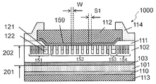
半導体素子1000は、第1導電型の半導体基板101と、半導体基板101の主面201上に配置された第1導電型の炭化珪素半導体層であるドリフト層102とを備えている。図1では、ドリフト層102と半導体基板101との間にバッファ層103を備えているが、バッファ層103を省略してもかまわない。ドリフト層102内には、第2導電型の終端領域151が配置されている。
ドリフト層102上には、第1電極159が配置されている。第1電極159は、ドリフト層102とショットキー接合を形成している。第1電極159は、炭化珪素半導体層であるドリフト層102と接する面の縁部において、終端領域151と接している。終端領域151と接する金属材料は第1電極159のみであってもよい。終端領域151は、第1電極159とは非オーミック接合を有していてもよい。
The
半導体基板101の主面201と対向する面である裏面上には、第2電極110が配置されている。第2電極110は、半導体基板101とオーミック接合を形成している。第2電極110の下面、すなわち半導体基板101と反対側の面には裏面電極113が配置されている。
The
図1に示すように、終端領域151は、第1電極159の一部と接する第2導電型のガードリング領域153、および、ガードリング領域153を囲むように配置された第2導電型のフローティング領域であるFLR領域154とを含んでいてもよい。FLR領域154は、ガードリング領域153と接触しないように配置されている。なお、終端領域151は、ドリフト層102の表面の一部を囲むように配置された少なくとも1つの領域を有していればよく、例示する構成に限定されない。
As shown in FIG. 1, the
半導体基板101の主面201の法線方向から見て、ドリフト層102における終端領域151の内側に位置する領域には、複数の第2導電型のバリア領域152が配置されていてもよい。バリア領域152を形成することにより、第1電極159およびドリフト層102にて形成されるショットキー接合に対して逆バイアスが印加された場合のショットキー漏れ電流を低減できる。
A plurality of second-conductivity-
終端領域151、ここではガードリング領域153およびFLR領域154は、第2導電型の高濃度領域121および第2導電型の低濃度領域122を有している。バリア領域152も、終端領域151と同様に、第2導電型の高濃度領域121および第2導電型の低濃度領域122を有していてもよい。高濃度領域121は、炭化珪素半導体層の表面(ここではドリフト層102の表面)202に接するように配置されている。低濃度領域122は、高濃度領域121の不純物濃度よりも低い濃度で第2導電型の不純物を含み、かつ、高濃度領域121より下方に位置している。また、半導体基板101の主面201の法線方向から見て、高濃度領域121と低濃度領域122とは同一の輪郭を有していてもよい。
The
図示する例では、ドリフト層102上には絶縁膜111が配置されている。絶縁膜111は、FLR領域154を覆い、かつ、ガードリング領域153の一部を覆っていてもよい。また、第1電極159の上には、第1電極159の上面および端面を覆うように上部電極112が配置されていてもよい。上部電極112の端面は絶縁膜111上に位置していてもよい。絶縁膜111の一部の上、および、上部電極112の一部の上には、パッシベーション膜114が配置されている。パッシベーション膜114は、上部電極112の上面の一部および端面を覆っていてもよい。
In the illustrated example, the insulating
図2は、半導体素子1000におけるドリフト層102の上面を例示する図であり、ドリフト層102を半導体基板101の主面201の法線方向から見た平面図である。図2では、説明を簡単にするために、ドリフト層102の表面202上に配置された電極などの構成要素を除去している。図1は、図2に示す1−1線に沿った断面に対応する。
FIG. 2 is a diagram illustrating the upper surface of the
図2に示す例では、各バリア領域152は、幅Wで一方向(以下、「第1の方向」)に延びるストライプ形状を有している。これらのバリア領域152は、第1の方向に直交する第2の方向に間隔S1を空けて、互いに平行になるように配置されている。このような配置により、各バリア領域152とドリフト層102との界面から延びる空乏層が、隣接するバリア領域152とドリフト層102との界面から延びる空乏層と均一につながるので、リーク電流をさらに抑制できる。
In the example shown in FIG. 2, each
半導体基板101の主面201の法線方向から見て、複数のバリア領域152のうち終端領域151に最も近いバリア領域152と、終端領域151との間隔の最大幅を距離S2とする。この例では、ガードリング領域153に最近接しているバリア領域152とガードリング領域153との間隔の最大幅が距離S2となる。「最大幅」は、上記間隔の第2の方向における最大距離を指す。また、FLR領域154の最も内側とガードリング領域153との間隔をS3とする。本実施形態では、隣接するバリア領域152間の間隔S1は距離S2以上であってもよい。あるいは、間隔S1は距離S2よりも大きくてもよい。さらに、距離S2は、ガードリング領域153とFLR領域154との間隔S3以上であってもよい。あるいは、距離S2は間隔S3よりも大きくてもよい。
When viewed from the normal direction of the
さらに、バリア領域152の第1の方向における端部は終端領域151と接していてもよい。この例では、バリア領域152の両端がガードリング領域153と接している。
Furthermore, the end portion of the
(半導体素子1000の動作)
金属と半導体からなるショットキー接合、及び半導体のpn接合に対して逆バイアスを印加すると、接合界面において空乏層が延びる。接合界面での電界強度がある値に到達すると、空乏層にアバランシェ電流が流れ、それ以上逆バイアスを印加できなくなる。本願ではこのアバランシェ電流が流れる電圧を単に「耐圧」と称する。
(Operation of Semiconductor Element 1000)
When a reverse bias is applied to a Schottky junction made of a metal and a semiconductor and a pn junction of a semiconductor, a depletion layer extends at the junction interface. When the electric field strength at the junction interface reaches a certain value, an avalanche current flows in the depletion layer and the reverse bias cannot be applied any more. In the present application, the voltage at which this avalanche current flows is simply referred to as "breakdown voltage".
以下、第1導電型をn型、第2導電型をp型として、半導体素子1000の動作を説明する。半導体素子1000はJBS構造を有している。半導体素子1000では、第2電極110に対して第1電極159に負の電圧を印加することによって、第1電極159とn型のドリフト層102との間に発生する空乏層がn型の半導体基板101側に延びる。また、p型のバリア領域152とn型のドリフト層102との間にはpn接合が形成されているため、このpn接合から主にドリフト層102側に空乏層が延びる。隣接するバリア領域152のpn接合からの空乏層が、隣接するバリア領域152の間にあるショットキー接合からのリーク電流を遮断することで、半導体素子1000のリーク電流が抑制される。一方で、耐圧は、ショットキー接合またはpn接合の接合界面における電界強度がある値に到達したところで決定される。終端領域151は、ドリフト層102表面における電界強度を緩和するために設けられる。
Hereinafter, the operation of the
(終端領域151の不純物濃度プロファイル)
半導体素子1000における終端領域151およびバリア領域152は、例えばイオン注入により同時に形成されてもよい。これにより、プロセスを簡便化でき、製造コストを低減できる。終端領域151およびバリア領域152は、例えば、ドリフト層102に対してAlイオンを注入することにより形成される。このとき、異なるエネルギーにてAlイオンを複数回注入することで、高濃度領域121と低濃度領域122とを有する終端領域151およびバリア領域152を同時に形成できる。なお、以下の説明では、ガードリング領域153およびFLR領域154を含む終端領域151とバリア領域152とを「p型注入領域」と総称する。
(Impurity concentration profile of termination region 151)
The
図3は、p型注入領域を形成する際のp型不純物イオン(ここではAlイオン)の深さ方向における注入プロファイルを例示する図である。「深さ方向」は、半導体基板101の主面201の法線方向を指す。
FIG. 3 is a diagram illustrating an implantation profile of p-type impurity ions (here, Al ions) in the depth direction when forming a p-type implantation region. “Depth direction” refers to a direction normal to the
プロファイルP1、P2は、いずれも、ドリフト層表面近傍に位置する高濃度領域と、高濃度領域よりも深い位置に低濃度領域とを有している。プロファイルP3は、ドリフト層表面近傍に高濃度領域を有していない比較例である。 Each of the profiles P1 and P2 has a high concentration region located near the surface of the drift layer and a low concentration region at a position deeper than the high concentration region. Profile P3 is a comparative example that does not have a high concentration region near the surface of the drift layer.
図3に示す例では、p型注入領域は、注入エネルギーの異なる4回のイオン注入工程によって形成されている。図3に示すイオン注入プロファイルは、例えば4回のイオン注入工程によって形成されたプロファイルを足し合わせたものである。ここでは、4回のイオン注入工程のうち、最も高エネルギーのイオン注入工程以外のイオン注入工程での注入ドーズ量を調整することにより、P1からP3までの3種類の注入プロファイルを作成している。 In the example shown in FIG. 3, the p-type implantation region is formed by four ion implantation steps with different implantation energies. The ion implantation profile shown in FIG. 3 is a combination of the profiles formed by, for example, four ion implantation steps. Here, among the four ion implantation steps, three types of implantation profiles P1 to P3 are created by adjusting the implantation dose amount in the ion implantation step other than the ion implantation step with the highest energy. ..
各イオン注入工程における注入エネルギーおよびドーズ量は例えば以下の通りである。 The implantation energy and dose amount in each ion implantation step are as follows, for example.

以下、注入された不純物イオンの活性化率が100%と仮定し、図3に示す注入プロファイルが、p型注入領域における深さ方向における不純物濃度プロファイルに相当するものとして説明する。 Hereinafter, it is assumed that the activation rate of the implanted impurity ions is 100% and the implantation profile shown in FIG. 3 corresponds to the impurity concentration profile in the p-type implantation region in the depth direction.
注入エネルギーの異なる複数回のイオン注入を利用して、高濃度領域121および低濃度領域122を含むp型注入領域を形成すると、その濃度プロファイルは、縦軸をLOGスケールで表示した図3に示すプロファイルP1、P2のように、高濃度領域121および低濃度領域122で、それぞれ、上に凸となる形状(以下、「凸部」)を有し得る。濃度プロファイルの凸部は、ピーク、サブピークだけでなく、ショルダーも含む。ショルダーとは、深さが大きくなるにつれて、プロファイルの傾き、すなわち濃度の減少率が低下して緩やかになる部分を指す。例えば、プロファイルP1では、高濃度領域121にピーク、低濃度領域122にショルダーを有している。終端領域151は、1×1018cm-3以上の濃度を有していてもよい。ここでいうピークおよびショルダー部分での濃度も1×1018cm-3以上であってもよい。このような構成により、高濃度領域または低濃度領域のみを有する従来のp型注入領域よりも耐圧を高めることができる。具体的には、p型注入領域の底部に低濃度領域122を有することにより、p型注入領域の底部の角部にかかる電界を低くできる。また、p型注入領域の上部に高濃度領域121を有することにより、p型注入領域の上部でp型注入領域の底部における角部よりも不純物濃度が高められるので、p型注入領域の底部の角部にかかる電界が、基板面に平行な方向に緩和される。このため、p型注入領域の底部の角部に生じる電界集中が緩和される結果、p型注入領域とドリフト層とのpn接合による耐圧の劣化を抑制できる。さらに、高濃度領域121の側面がドリフト層102と直接接することから、終端領域151において、高濃度領域121とドリフト層102との間に形成されるpn接合界面がよりドリフト層102側にシフトするため、隣り合うp型注入領域の実効的な間隔をより小さくすることが可能となる。このため、終端領域151で決定される耐圧を向上させることができ、半導体素子1000の素子耐圧が終端領域151側で律速している場合には、素子耐圧をさらに向上できる。
When the p-type implantation region including the high-
これに対し、例えば、イオン注入を複数回行わずにp型注入領域を形成すると、その注入プロファイルは、所定の深さでのみ凸部となるピークを有し、それよりも深い領域(テール)では1×1018cm-3以上の濃度領域においてショルダーなどの凸部を有さないことがある。このような場合には、p型注入領域の不純物濃度を、本実施形態の低濃度領域と同程度に低く設定しても、あるいは高濃度領域と同程度に高く設定しても、上記効果は得られず、耐圧の劣化が生じ得る。 On the other hand, for example, when a p-type implantation region is formed without performing ion implantation a plurality of times, the implantation profile has a peak that becomes a convex portion only at a predetermined depth, and a region deeper than that (tail). In some cases, there is no protrusion such as a shoulder in the concentration region of 1×10 18 cm −3 or more. In such a case, even if the impurity concentration of the p-type implantation region is set to be as low as that of the low concentration region of the present embodiment or is set to be as high as that of the high concentration region, the above effect is obtained. If not obtained, the breakdown voltage may deteriorate.
低濃度領域122は、高濃度領域121を形成する不純物注入エネルギーに比べて、より大きなエネルギーで注入することによって形成されてもよい。これにより、例えば図3に例示するプロファイルP2、P3にみられるように、深さが例えば0.3から0.4μmの位置に、ドリフト層102の表面、すなわち深さ0μm近傍に位置するピークとは異なるピークまたはサブピークを有し得る。また、プロファイルP1では、同様の位置にピークまたはサブピークは見られないものの、凸部となる緩やかなショルダーが見られる。なお、低濃度領域122を形成するためのイオン注入方法は上記方法に限定されない。比較的小さいエネルギーによるイオン注入を複数回行うことによって、所定の深さにショルダーを含むプロファイルを有する低濃度領域122を形成することも可能である。
The low-
本実施形態におけるp型注入領域の濃度プロファイルは図示する例に限定されない。p型注入領域を形成する際のイオン注入条件および注入工程の回数により、濃度プロファイルの形状は変化し得る。イオン注入条件および濃度プロファイルの形状などが異なる場合でも、p型注入領域が高濃度領域121および低濃度領域122を含んでいれば、上記と同様の効果が得られる。
The concentration profile of the p-type implantation region in this embodiment is not limited to the illustrated example. The shape of the concentration profile may change depending on the ion implantation conditions and the number of implantation steps when forming the p-type implantation region. Even if the ion implantation conditions and the shape of the concentration profile are different, if the p-type implantation region includes the
濃度が所定の濃度を超えない領域を低濃度領域122、濃度が所定の濃度以上となる領域を高濃度領域121と定義してもよい。所定の濃度は、例えば1×1019cm-3であってもよい。このように定義する場合には、プロファイルP1における高濃度領域121は表面から深さ約0.3μm程度まで、プロファイルP2における高濃度領域121は表面から深さ約0.2μm程度までの領域となる。また、プロファイルP3には、不純物濃度が1×1019cm-3以上となる領域が存在しないため、高濃度領域121を含まず、全領域が低濃度領域122となる。なお、所定の濃度は1×1020cm-3であってもよい。
An area where the density does not exceed a predetermined density may be defined as a
次いで、JBS構造を有する素子において、終端領域の濃度プロファイルと耐圧との関係を検討した結果を説明する。 Next, the result of examining the relationship between the concentration profile of the termination region and the breakdown voltage in the element having the JBS structure will be described.
終端領域の濃度プロファイルが異なる素子D1、D2、D3に対し、耐圧測定を実施したときの累積度数分布を調べた。素子D1、D2、D3は、それぞれ、図3に示すプロファイルP1、P2、P3と同様の濃度プロファイルを有する終端領域を備えたJBS構造を有する素子である。素子D1、D2、D3の構成は、図1に示す半導体素子1000と同様である。耐圧測定の結果を図4に示す。
For the devices D1, D2, and D3 having different concentration profiles in the termination region, the cumulative frequency distribution when the breakdown voltage was measured was examined. The devices D1, D2, and D3 are devices having a JBS structure having a termination region having a concentration profile similar to the profiles P1, P2, and P3 shown in FIG. 3, respectively. The configurations of the elements D1, D2, and D3 are similar to those of the
図4に示す結果から、終端領域に高濃度領域を有していない素子D3の耐圧は、他の素子D1、D2よりも低くなることが確認された。また、高濃度領域121の濃度の高い素子D1は、素子D2よりも高い耐圧を有することが明らかとなった。図4からmedian値を読み取ると、素子D1、D2、D3における耐圧は、それぞれ、1510V、1410V、1280Vとなった。これらの素子では、ドリフト層102の濃度および厚さほぼ同等であり、濃度プロファイル以外の素子構造も同じである。このため、これらの素子間の耐圧の差はプロファイルP1、P2、P3の違いによりもたらされたものといえる。この例では、高濃度領域の不純物濃度は、例えば1×1019cm-3以上であれば耐圧向上効果が得られることが分かる。また、高濃度領域の不純物濃度が1×1020cm-3以上であればより効果的に耐圧を向上できることが分かる。
From the results shown in FIG. 4, it was confirmed that the breakdown voltage of the device D3 having no high concentration region in the termination region was lower than that of the other devices D1 and D2. Further, it has been clarified that the element D1 having a high concentration in the
前述のように、終端領域151はドリフト層102表面における電界強度を緩和するために存在している。電界強度の緩和は空乏層の延び方により影響を受ける。たとえばFLR領域154の本数を増やすことにより、ドリフト層102の表面に平行な方向の空乏層がドリフト層102内で延びやすくなることで、終端領域151における電界強度が緩和される。pn接合界面から延びる空乏層は、p型領域およびn型領域の両方に形成される。しかし、p型領域の濃度を大きくすることにより、pn接合界面から延びる空乏層はp型領域側に延びにくくなり、pn接合付近の電界分布が変化する。これによりドリフト層102の表面に平行な方向のn型ドリフト層102に延びる空乏層の延び方が変化して、さらなる電界緩和が実現できる。
As described above, the
なお、炭化珪素に不純物注入にてp型領域を形成する場合、p型領域内に結晶欠陥が残存する場合がある。第1電極159と接するバリア領域152およびガードリング領域153内に結晶欠陥があると、バリア領域152およびガードリング領域153とn型ドリフト層102との間に形成されるpn接合からのリーク電流の発生が懸念される。この問題は、ドリフト層102の表面に垂直な方向を横切るpn接合を、より低濃度なp型領域を用いて形成することによって回避できる。したがって、終端領域およびバリア領域となるp型領域を高濃度領域121および低濃度領域122の組み合わせにて形成することにより、高耐圧と低リークとを両立させる半導体素子1000を実現できる。
When a p-type region is formed in silicon carbide by implanting impurities, crystal defects may remain in the p-type region. When there is a crystal defect in the
以上で述べたように、半導体素子1000において、終端領域における不純物の濃度プロファイルが異なると、ドリフト層102の濃度、厚さが同等であっても耐圧が変化する。従って、濃度プロファイルを制御することによって、高耐圧な半導体素子1000を実現することが可能になる。あるいは、十分な耐圧を確保しつつ、順方向のオン電圧を低減することが可能になる。例えば1000Vの逆方向電圧に耐える半導体素子1000を作製することを要求されている場合、ドリフト層102の濃度、厚さの面内分布、及びドリフト層ごとのばらつきを考慮して耐圧が例えば1300V程度の半導体素子1000を作製することがある。例えば濃度プロファイルがP3である素子D3で耐圧1300Vを実現したと仮定する。このときのドリフト層102の濃度をn3、厚さをd3とする。このドリフト層102と同じ濃度および厚さを用いて、濃度プロファイルがP1である素子D1を作製すると、耐圧は例えば1500V程度にまで向上し得る。ここで、ドリフト層102の濃度または厚さ、またはその両方を選択しなおし、耐圧が1300V前後になるように調整する。耐圧を約200Vほど低下させてもよいことになるので、例えば、ドリフト層102の濃度を高く設定する、またはドリフト層102の厚さを小さくすることが可能となる。ドリフト層102の高濃度化または薄膜化は、いずれもドリフト抵抗を低減させる要因となる。つまり、素子D3に比べて素子D1は同じ耐圧であってもドリフト層の高濃度化または薄膜化を実現できるので、順方向の抵抗が小さくなる。したがって、半導体素子1000のオン電圧低減が実現できる。
As described above, in the
(半導体素子の製造方法)
次に、本実施形態に係る半導体素子1000の製造方法について図5から図13を用いて説明する。図5から図13は、本実施形態に係る半導体素子1000の製造方法の一部を示す断面図である。
(Method of manufacturing semiconductor element)
Next, a method for manufacturing the
まず、半導体基板101を準備する。半導体基板101は、例えば、抵抗率が0.02Ωcm程度である低抵抗のn型4H−SiCオフカット基板である。
First, the
図5に示すように、半導体基板101の上に高抵抗でn型のドリフト層102をエピタキシャル成長により形成する。ドリフト層102を形成する前に、半導体基板101上に、n型で高不純物濃度のSiCによって構成されるバッファ層103を堆積してもよい。バッファ層の不純物濃度は、例えば、1×1018cm-3であり、バッファ層の厚さは、例えば、1μmである。ドリフト層102は、例えば、n型4H−SiCによって構成され、不純物濃度及び厚さは、例えばそれぞれ1×1016cm-3及び10μmである。
As shown in FIG. 5, a high-resistance n-
次に、図6に示すように、ドリフト層102の上に、例えばSiO2からなるマスク160を形成した後、例えばAlイオンをドリフト層102に注入する。これにより、ドリフト層102に、イオン注入領域1510、1520、1530および1540を形成する。イオン注入領域1510、1520、1530および1540は、それぞれ、後に、終端領域151、バリア領域152、ガードリング領域153、およびFLR領域154となる。
Next, as shown in FIG. 6, after forming a
イオン注入領域1510、1520、1530および1540は、ドリフト層102の表面側に高濃度注入領域1210、それより深い領域に低濃度注入領域1220を有する。高濃度注入領域1210および低濃度注入領域1220におけるAlイオンの濃度プロファイルが、例えば、図3で示したプロファイルP1またはP2に代表されるようなプロファイルを有するように、イオン注入のエネルギーとドーズ量とを調整してもよい。この注入を同時に実施することにより、終端領域151およびバリア領域152の、半導体基板101の主面に垂直な方向における不純物濃度の濃度プロファイルは同じとなる。また、同一のマスク160を用いて、後に高濃度領域121および低濃度領域122となる高濃度注入領域1210および低濃度注入領域1220を同時に形成する。これにより、半導体基板101の主面に垂直な方向からみて、終端領域151およびバリア領域152における、高濃度領域121および低濃度領域122の輪郭は略同一となる。
The
なお、図示していないが、必要に応じて半導体基板101の裏面側に対して、第1導電型の不純物注入を行い、裏面側の第1導電型濃度をさらに高めてもよい。
Although not shown, if necessary, the first conductivity type impurity may be implanted into the back surface side of the
次に、図7に示すように、マスク160を除去後、1500から1900℃程度の温度で熱処理することにより、イオン注入領域1510、1520、1530および1540から、それぞれ、終端領域151、バリア領域152、ガードリング領域153およびFLR領域154が形成される。なお、熱処理実施前にドリフト層102の表面にカーボン膜を堆積し、熱処理後にカーボン膜を除去してもよい。また、その後に、ドリフト層102表面に熱酸化膜を形成後、その熱酸化膜をエッチングで除去することにより、ドリフト層102表面を清浄化してもよい。図1に示す隣接するバリア領域152の幅Wは例えば2μmであり、間隔S1は例えば4μmである。ガードリング領域153の幅は例えば15μm程度である。図1に示すバリア領域152とガードリング領域153との距離S2は、例えば3μmであり、間隔S1以下に設定される。ガードリング領域153と最も内側のFLR領域154との間隔S3は例えば1μmである。
Next, as shown in FIG. 7, after removing the
次に、図8に示すように、半導体基板101の裏面側に、例えばNiを200nm程度堆積した後、約1000℃で熱処理することにより第2電極110を形成する。第2電極110は半導体基板101の裏面とオーミック接合を形成する。
Next, as shown in FIG. 8, for example, Ni is deposited to a thickness of about 200 nm on the back surface side of the
次に、ドリフト層102表面に例えばSiO2からなる絶縁膜111を形成する。絶縁
膜111の厚さは例えば300nmである。次にフォトレジストによるマスクを形成して例えばウェットエッチングによりガードリング領域153の一部、および、ガードリング領域153の内側のドリフト層102を露出させる。その後マスクを除去する。このようにして、図9に示すように、開口を有する絶縁膜111が得られる。
Next, an insulating
次に、開口を有する絶縁膜111および開口部に露出したドリフト層102の全面を覆うように、第1電極用導電膜が堆積される。第1電極用導電膜は例えば、Ti、Ni、Mo等である。第1電極用導電膜の厚さは例えば200nmである。この後フォトレジストによるマスクを形成して、少なくとも絶縁膜111から露出したドリフト層102を覆う部分が残るように第1電極用導電膜をパターニングすることにより、第1電極159を得る。図10の例では、第1電極159の端部は絶縁膜111上にある。第1電極159は、暴露されたドリフト層102、およびガードリング領域153の一部と接している。その後、第1電極159を有する半導体基板101を100℃以上700℃以下の温度で熱処理する。これにより、第1電極159は、ドリフト層102とショットキー接合を形成する。
Next, a conductive film for the first electrode is deposited so as to cover the entire surface of the insulating
次に、第1電極159および絶縁膜111の上方に上部電極用導電膜を堆積する。上部電極用導電膜は、例えばAlを含む4μm程度の金属膜である。上部電極用導電膜上にマスクを形成して不要な部分をエッチングすることで絶縁膜111の一部を露出させる。上部電極用導電膜をウェットエッチングする際には、第1電極159が露出しないように上部電極用導電膜のエッチング条件を調整してもよい。上部電極用導電膜の一部をエッチングした後にマスクを除去することで、図11に示すような上部電極112が形成される。
Next, a conductive film for an upper electrode is deposited above the
次に、必要に応じて図12に示したパッシベーション膜114を形成する。まず、露出した絶縁膜111および上部電極112の上方に、例えばSiNからなるパッシベーション膜114を形成する。その後、上部電極112の上部に形成されたパッシベーション膜114が暴露するような開口を有するマスクを準備し、例えばドライエッチングによりパッシベーション膜の一部をエッチングして上部電極112の一部を露出させる。その後、マスクを除去する。これにより、図12に示すように、上部電極112上の一部が開口されたパッシベーション膜114が得られる。パッシベーション膜114は絶縁体であればよく、例えばSiO2膜でもよいし、ポリイミドなどの有機膜であってもよい。
Next, the
次に、図13に示すように、必要に応じて裏面電極113が形成される。裏面電極113の形成プロセスは、上記のパッシベーション膜114の形成工程の前であってもよいし、上部電極112の形成工程の前であってもよい。裏面電極113は、例えば、第2電極110に接する側から、Ti、Ni、Agの順に堆積する。それぞれの厚さは、例えば0.1μm、0.3μm、0.7μmである。以上の工程を経て、半導体素子1000が形成される。
Next, as shown in FIG. 13, a
(変形例)
以下、本実施形態の半導体素子の変形例を説明する。
(Modification)
Hereinafter, modified examples of the semiconductor device of this embodiment will be described.
図14は、変形例1の半導体素子2000を示す断面図である。図15は、半導体素子2000における炭化珪素半導体層の表面を説明するための平面図である。図14は、図15に示す14−14線に沿った断面に対応する。
FIG. 14 is a cross-sectional view showing a
変形例1の半導体素子2000は、バリア領域が設けられていない通常のSBD構造を有する。半導体素子2000は、バリア領域を有さない以外は図1に示す半導体素子1000と同様の構成を有する。半導体素子2000における終端領域151の濃度プロファイルは、例えば図3に示したプロファイルP1またはP2と同様であってもよい。
The
半導体素子2000の終端領域151は、高濃度領域121および低濃度領域122を有しているので、上記と同様の耐圧を向上させる効果が得られる。従って、終端領域151が低濃度領域または高濃度領域のみを有する半導体素子よりも高い耐圧を実現できる。
Since the
図16は、変形例2の半導体素子3000を示す断面図である。図17は、半導体素子3000における炭化珪素半導体層の表面を説明するための平面図である。図16は、図17に示す16−16線に沿った断面に対応する。
FIG. 16 is a sectional view showing a
変形例2の半導体素子3000は、複数のバリア領域152を有するJBS構造の半導体素子である。各バリア領域152は四角形の平面形状を有している。バリア領域152の形状以外は、図1に示す半導体素子1000と同様の構成を有する。半導体素子3000における終端領域151の濃度プロファイルは、例えば図3に示したプロファイルP1またはP2と同様であってもよい。
The
半導体素子3000の終端領域151は、高濃度領域121および低濃度領域122を有しているので、上記と同様の耐圧を向上させる効果が得られる。従って、終端領域151が低濃度領域または高濃度領域のみを有する半導体素子よりも高い耐圧を実現できる。また、半導体素子3000はバリア領域152を有するので、バリア領域を有していない半導体素子2000よりもリーク電流を低減できる。
Since the
本開示の半導体素子の構成および各構成要素の材料は、上記に例示した構成および材料に限定されない。例えば、第1電極159の材料は、上記に例示したTi、NiおよびMoに限定されない。第1電極159は、ドリフト層102とショットキー接合するその他の金属、並びにそれらの合金及び化合物からなる群から選択したものを使用してもよい。
The configuration of the semiconductor element of the present disclosure and the material of each component are not limited to the configurations and materials illustrated above. For example, the material of the
また、第1電極159の上部であって、上部電極112の下部に、例えばTiNを含むバリア膜を形成してもよい。バリア膜の厚さは、例えば50nmである。
Further, a barrier film containing, for example, TiN may be formed above the
また、本開示の実施形態では、炭化珪素が4H−SiCである例について説明したが、炭化珪素は6H−SiC、3C−SiC、15R−SiCなどの他のポリタイプであってもよい。また、本開示の実施形態では、SiC基板の主面が(0001)面からオフカットした面である例について説明したが、SiC基板の主面は、(11−20)面、(1−100)面、(000−1)面、またはこれらのオフカット面であってもよい。また、半導体基板101としてSi基板を用いてもよい。Si基板上に、3C−SiCドリフト層を形成してもよい。この場合、3C−SiCに注入された不純物イオンを活性化するためのアニールを、Si基板の融点以下の温度で実施してもよい。
Further, in the embodiment of the present disclosure, an example in which the silicon carbide is 4H-SiC has been described, but the silicon carbide may be another polytype such as 6H-SiC, 3C-SiC, and 15R-SiC. Further, in the embodiment of the present disclosure, an example in which the main surface of the SiC substrate is a surface off-cut from the (0001) surface has been described, but the main surface of the SiC substrate is the (11-20) surface, (1-100) ) Plane, (000-1) plane, or their off-cut planes. A Si substrate may be used as the
本開示は、例えば、民生用、車載用、産業機器用等の電力変換器に搭載するためのパワー半導体デバイスに用いられ得る。 The present disclosure can be used in, for example, a power semiconductor device for mounting on a power converter for consumer use, vehicle mounting, industrial equipment, and the like.
1000、2000、3000 半導体素子
101 半導体基板
102 ドリフト層
103 バッファ層
110 第2電極
111 絶縁膜
112 上部電極
113 裏面電極
114 パッシベーション膜
121 高濃度領域
122 低濃度領域
151 終端領域
152 バリア領域
153 ガードリング領域
154 FLR領域
159 第1電極
160 マスク
201 主面
202 表面
1000, 2000, 3000
Claims (7)
前記半導体基板の前記主面上に配置された第1導電型の炭化珪素半導体層と、
前記炭化珪素半導体層内に配置された第2導電型のガードリング領域と、
前記炭化珪素半導体層内に配置された第2導電型のフローティング領域と、
前記炭化珪素半導体層上に配置され、前記炭化珪素半導体層とショットキー接合を形成する第1電極と、
前記半導体基板の前記裏面上に配置され、前記半導体基板とオーミック接合を形成する第2電極と、
前記主面の法線方向から見て、前記ガードリング領域に囲まれた前記炭化珪素半導体層内に配置された複数の第2導電型のバリア領域と、を備え、
前記ガードリング領域は、前記主面の法線方向から見て前記炭化珪素半導体層表面の一部を囲むように配置されており、
前記第1電極は、前記炭化珪素半導体層と接する面を有し、
前記第1電極は、前記炭化珪素半導体層と接する前記面の縁部において、前記ガードリング領域と接し、
前記フローティング領域は、前記主面の法線方向から見て前記ガードリング領域を囲み、かつ前記ガードリング領域と接触しておらず、
前記ガードリング領域、前記フローティング領域および前記複数の第2導電型のバリア領域の各々は、前記炭化珪素半導体層の表面に接する第2導電型の高濃度領域と、前記高濃度領域より下方に位置する第2導電型の低濃度領域とを含み、
前記高濃度領域の不純物濃度は、前記低濃度領域の不純物濃度よりも高く、
前記主面の法線方向から見て、前記高濃度領域と前記低濃度領域とは同一の輪郭を有しており、
前記高濃度領域の前記不純物濃度は、1×1020cm−3以上であり、前記低濃度領域の前記不純物濃度は、1×1020cm−3未満であり、
前記主面の法線方向から見て、前記複数の第2導電型のバリア領域のそれぞれは、第1の方向に延びる形状を有し、
前記複数の第2導電型のバリア領域は、前記第1の方向に直交する第2の方向に第1間隔を空けて配列されており、
前記複数の第2導電型のバリア領域のそれぞれにおける前記第1の方向の両端は、前記ガードリング領域と接続されており、
前記主面の法線方向から見て、前記複数の第2導電型のバリア領域のうち前記ガードリング領域に最も近いバリア領域と、前記ガードリング領域との間隔である第2間隔の、前記第2の方向における最大幅は、前記第1間隔より小さい、半導体素子。 A first conductivity type semiconductor substrate having a main surface and a back surface;
A first conductivity type silicon carbide semiconductor layer disposed on the main surface of the semiconductor substrate;
A second conductivity type guard ring region arranged in the silicon carbide semiconductor layer;
A second conductivity type floating region disposed in the silicon carbide semiconductor layer;
A first electrode disposed on the silicon carbide semiconductor layer and forming a Schottky junction with the silicon carbide semiconductor layer;
A second electrode disposed on the back surface of the semiconductor substrate and forming an ohmic contact with the semiconductor substrate;
A plurality of second-conductivity-type barrier regions arranged in the silicon carbide semiconductor layer surrounded by the guard ring region when viewed from the direction normal to the main surface,
The guard ring region is arranged so as to surround a part of the surface of the silicon carbide semiconductor layer when viewed from the direction normal to the main surface,
The first electrode has a surface in contact with the silicon carbide semiconductor layer,
The first electrode is in contact with the guard ring region at an edge of the surface in contact with the silicon carbide semiconductor layer,
The floating region surrounds the guard ring region when viewed from the normal direction of the main surface, and is not in contact with the guard ring region,
Each of the guard ring region, the floating region, and the plurality of second conductivity type barrier regions is located below the second conductivity type high concentration region in contact with the surface of the silicon carbide semiconductor layer and below the high concentration region. And a low-concentration region of the second conductivity type,
The impurity concentration of the high concentration region is higher than the impurity concentration of the low concentration region,
The high-concentration region and the low-concentration region have the same contour as viewed from the normal direction of the main surface,
The impurity concentration of the high concentration region is 1 × 10 20 cm -3 or more, the impurity concentration of the low concentration region state, and are less than 1 × 10 20 cm -3,
Each of the plurality of second conductivity type barrier regions has a shape extending in the first direction when viewed from the direction normal to the main surface,
The plurality of second conductivity type barrier regions are arranged at a first interval in a second direction orthogonal to the first direction,
Both ends of each of the plurality of second conductivity type barrier regions in the first direction are connected to the guard ring region,
Of the plurality of second-conductivity-type barrier regions as seen from the direction normal to the main surface, the barrier region closest to the guard ring region and the second interval, which is the interval between the guard ring region and the second interval, A semiconductor device having a maximum width in the direction 2 that is smaller than the first interval .
前記第1電極の上面に配置された上部電極と
をさらに備え、
前記上部電極は前記第1電極の上面および端面を覆い、
前記上部電極の端面は前記絶縁膜上にある、請求項1から6のいずれかに記載の半導体素子。 An insulating film covering at least a part of the guard ring region,
Further comprising an upper electrode disposed on the upper surface of the first electrode,
The upper electrode covers an upper surface and an end surface of the first electrode,
The end face of the upper electrode is on the insulating film, a semiconductor device according to any one of claims 1 to 6.
Applications Claiming Priority (2)
| Application Number | Priority Date | Filing Date | Title |
|---|---|---|---|
| JP2015083369 | 2015-04-15 | ||
| JP2015083369 | 2015-04-15 |
Publications (2)
| Publication Number | Publication Date |
|---|---|
| JP2016208016A JP2016208016A (en) | 2016-12-08 |
| JP6745458B2 true JP6745458B2 (en) | 2020-08-26 |
Family
ID=57129320
Family Applications (1)
| Application Number | Title | Priority Date | Filing Date |
|---|---|---|---|
| JP2016059482A Active JP6745458B2 (en) | 2015-04-15 | 2016-03-24 | Semiconductor element |
Country Status (2)
| Country | Link |
|---|---|
| US (1) | US20160308072A1 (en) |
| JP (1) | JP6745458B2 (en) |
Families Citing this family (6)
| Publication number | Priority date | Publication date | Assignee | Title |
|---|---|---|---|---|
| DE102016104968B3 (en) * | 2016-03-17 | 2017-07-27 | Infineon Technologies Ag | METHOD FOR PRODUCING SEMICONDUCTOR DEVICES WITH TRANSISTOR CELLS, SEMICONDUCTOR DEVICE AND MICROELECTROMECHANICAL DEVICE |
| JP6719090B2 (en) * | 2016-12-19 | 2020-07-08 | パナソニックIpマネジメント株式会社 | Semiconductor element |
| CN106887470B (en) * | 2017-01-23 | 2019-07-16 | 西安电子科技大学 | Ga2O3Schottky diode device structure and preparation method thereof |
| JP7259609B2 (en) * | 2019-07-17 | 2023-04-18 | 株式会社デンソー | semiconductor equipment |
| CN112233981A (en) * | 2020-10-13 | 2021-01-15 | 长江存储科技有限责任公司 | Semiconductor device and method for manufacturing the same |
| CN114927535B (en) * | 2022-05-20 | 2023-09-22 | 无锡鉴微华芯科技有限公司 | X-ray detector with double three-dimensional full-surrounding protection ring and preparation method thereof |
Family Cites Families (30)
| Publication number | Priority date | Publication date | Assignee | Title |
|---|---|---|---|---|
| EP1065726B1 (en) * | 1998-03-19 | 2010-01-13 | Hitachi, Ltd. | Silicon carbide junction-gate field effect transistor |
| JP4892787B2 (en) * | 2001-04-09 | 2012-03-07 | 株式会社デンソー | Schottky diode and manufacturing method thereof |
| US8901699B2 (en) * | 2005-05-11 | 2014-12-02 | Cree, Inc. | Silicon carbide junction barrier Schottky diodes with suppressed minority carrier injection |
| US20070138482A1 (en) * | 2005-12-08 | 2007-06-21 | Nissan Motor Co., Ltd. | Silicon carbide semiconductor device and method for producing the same |
| JP2007235064A (en) * | 2006-03-03 | 2007-09-13 | Matsushita Electric Ind Co Ltd | Schottky barrier semiconductor device, and method of manufacturing same |
| JP4420062B2 (en) * | 2007-05-10 | 2010-02-24 | 株式会社デンソー | Silicon carbide semiconductor device having junction barrier Schottky diode |
| JP4356767B2 (en) * | 2007-05-10 | 2009-11-04 | 株式会社デンソー | Silicon carbide semiconductor device having junction barrier Schottky diode |
| JP4375439B2 (en) * | 2007-05-30 | 2009-12-02 | 株式会社デンソー | Silicon carbide semiconductor device having junction barrier Schottky diode |
| JP4333782B2 (en) * | 2007-07-05 | 2009-09-16 | 株式会社デンソー | Silicon carbide semiconductor device having junction barrier Schottky diode |
| JP2009059764A (en) * | 2007-08-30 | 2009-03-19 | Panasonic Corp | Schottky barrier diode, and manufacturing method thereof |
| JP2009130266A (en) * | 2007-11-27 | 2009-06-11 | Toshiba Corp | Semiconductor substrate and semiconductor device, and method of manufacturing the same |
| JP2010087195A (en) * | 2008-09-30 | 2010-04-15 | Panasonic Corp | Semiconductor device |
| JP4796665B2 (en) * | 2009-09-03 | 2011-10-19 | パナソニック株式会社 | Semiconductor device and manufacturing method thereof |
| JP5172916B2 (en) * | 2010-09-08 | 2013-03-27 | 株式会社東芝 | Semiconductor rectifier |
| US8563988B2 (en) * | 2010-10-29 | 2013-10-22 | Panasonic Corporation | Semiconductor element and manufacturing method therefor |
| JP5644536B2 (en) * | 2011-01-21 | 2014-12-24 | 三菱電機株式会社 | Power semiconductor device |
| WO2013121532A1 (en) * | 2012-02-15 | 2013-08-22 | 富士電機株式会社 | Wide band gap semiconductor device |
| US9536942B2 (en) * | 2012-03-15 | 2017-01-03 | Mitsubishi Electric Corporation | Semiconductor device having a plurality of electric field relaxation layers and method for manufacturing same |
| WO2013145545A1 (en) * | 2012-03-30 | 2013-10-03 | 三菱電機株式会社 | Semiconductor device |
| JP5812029B2 (en) * | 2012-06-13 | 2015-11-11 | 株式会社デンソー | Silicon carbide semiconductor device and manufacturing method thereof |
| JP5811977B2 (en) * | 2012-09-18 | 2015-11-11 | 株式会社デンソー | Silicon carbide semiconductor device |
| JP5628462B1 (en) * | 2012-12-03 | 2014-11-19 | パナソニック株式会社 | Semiconductor device and manufacturing method thereof |
| JP6028676B2 (en) * | 2013-05-21 | 2016-11-16 | 住友電気工業株式会社 | Silicon carbide semiconductor device |
| JP6244665B2 (en) * | 2013-05-29 | 2017-12-13 | 住友電気工業株式会社 | Semiconductor device |
| US20160254357A1 (en) * | 2013-10-24 | 2016-09-01 | Rohm Co., Ltd. | Semiconductor device and semiconductor package |
| JP6065154B2 (en) * | 2014-04-30 | 2017-01-25 | 三菱電機株式会社 | Silicon carbide semiconductor device |
| JP6356592B2 (en) * | 2014-12-17 | 2018-07-11 | トヨタ自動車株式会社 | Schottky barrier diode and manufacturing method thereof |
| DE112015002153T5 (en) * | 2014-12-25 | 2017-01-26 | Fuji Electric Co., Ltd. | Semiconductor device |
| JP2016201448A (en) * | 2015-04-09 | 2016-12-01 | トヨタ自動車株式会社 | Diode and method for manufacturing diode |
| US9773924B2 (en) * | 2015-04-22 | 2017-09-26 | Panasonic Intellectual Property Management Co., Ltd. | Semiconductor device having barrier region and edge termination region enclosing barrier region |
-
2016
- 2016-03-24 JP JP2016059482A patent/JP6745458B2/en active Active
- 2016-04-01 US US15/089,383 patent/US20160308072A1/en not_active Abandoned
Also Published As
| Publication number | Publication date |
|---|---|
| US20160308072A1 (en) | 2016-10-20 |
| JP2016208016A (en) | 2016-12-08 |
Similar Documents
| Publication | Publication Date | Title |
|---|---|---|
| JP6745458B2 (en) | Semiconductor element | |
| JP6624592B2 (en) | Semiconductor device and method of manufacturing the same | |
| JP6202944B2 (en) | Silicon carbide semiconductor device and manufacturing method thereof | |
| JP5452718B2 (en) | Semiconductor device | |
| TWI596783B (en) | Semiconductor device | |
| JP6065154B2 (en) | Silicon carbide semiconductor device | |
| JP7113220B2 (en) | Semiconductor device and manufacturing method thereof | |
| US8890169B2 (en) | Semiconductor device | |
| US9178079B2 (en) | Semiconductor diode device | |
| JP6010773B2 (en) | Semiconductor device and manufacturing method thereof | |
| CN108735720B (en) | Semiconductor device with a plurality of semiconductor chips | |
| US10096703B2 (en) | Semiconductor device and method of manufacturing semiconductor device | |
| JP2009105200A (en) | Junction barrier schottky diode | |
| JP7113230B2 (en) | semiconductor element | |
| KR101416361B1 (en) | Shottky barrier diode and method for manufacturing the same | |
| JP6125748B2 (en) | Semiconductor device | |
| JP7030665B2 (en) | Semiconductor device | |
| US9947806B2 (en) | Semiconductor device | |
| JP2017201683A (en) | Semiconductor element | |
| JP5755722B2 (en) | Semiconductor device | |
| JP5476439B2 (en) | Junction barrier Schottky diode | |
| JP6651801B2 (en) | Semiconductor device and method of manufacturing semiconductor device | |
| JP2017098578A (en) | Silicon carbide semiconductor device and manufacturing method of the same | |
| EP4036986A1 (en) | Silicon carbide vertical conduction mosfet device and manufacturing process thereof | |
| JP2024060452A (en) | Semiconductor device and its manufacturing method |
Legal Events
| Date | Code | Title | Description |
|---|---|---|---|
| A621 | Written request for application examination |
Free format text: JAPANESE INTERMEDIATE CODE: A621 Effective date: 20181011 |
|
| A977 | Report on retrieval |
Free format text: JAPANESE INTERMEDIATE CODE: A971007 Effective date: 20190614 |
|
| A131 | Notification of reasons for refusal |
Free format text: JAPANESE INTERMEDIATE CODE: A131 Effective date: 20190709 |
|
| A521 | Request for written amendment filed |
Free format text: JAPANESE INTERMEDIATE CODE: A523 Effective date: 20190808 |
|
| A131 | Notification of reasons for refusal |
Free format text: JAPANESE INTERMEDIATE CODE: A131 Effective date: 20200107 |
|
| A521 | Request for written amendment filed |
Free format text: JAPANESE INTERMEDIATE CODE: A523 Effective date: 20200122 |
|
| A02 | Decision of refusal |
Free format text: JAPANESE INTERMEDIATE CODE: A02 Effective date: 20200428 |
|
| A521 | Request for written amendment filed |
Free format text: JAPANESE INTERMEDIATE CODE: A523 Effective date: 20200527 |
|
| A911 | Transfer to examiner for re-examination before appeal (zenchi) |
Free format text: JAPANESE INTERMEDIATE CODE: A911 Effective date: 20200605 |
|
| TRDD | Decision of grant or rejection written | ||
| A01 | Written decision to grant a patent or to grant a registration (utility model) |
Free format text: JAPANESE INTERMEDIATE CODE: A01 Effective date: 20200714 |
|
| A61 | First payment of annual fees (during grant procedure) |
Free format text: JAPANESE INTERMEDIATE CODE: A61 Effective date: 20200716 |
|
| R151 | Written notification of patent or utility model registration |
Ref document number: 6745458 Country of ref document: JP Free format text: JAPANESE INTERMEDIATE CODE: R151 |