JP6719090B2 - Semiconductor element - Google Patents
Semiconductor element Download PDFInfo
- Publication number
- JP6719090B2 JP6719090B2 JP2016245590A JP2016245590A JP6719090B2 JP 6719090 B2 JP6719090 B2 JP 6719090B2 JP 2016245590 A JP2016245590 A JP 2016245590A JP 2016245590 A JP2016245590 A JP 2016245590A JP 6719090 B2 JP6719090 B2 JP 6719090B2
- Authority
- JP
- Japan
- Prior art keywords
- region
- semiconductor
- layer
- surface electrode
- semiconductor element
- Prior art date
- Legal status (The legal status is an assumption and is not a legal conclusion. Google has not performed a legal analysis and makes no representation as to the accuracy of the status listed.)
- Active
Links
- 239000004065 semiconductor Substances 0.000 title claims description 319
- 239000010410 layer Substances 0.000 claims description 317
- 229910052751 metal Inorganic materials 0.000 claims description 155
- 239000002184 metal Substances 0.000 claims description 155
- 239000011241 protective layer Substances 0.000 claims description 129
- 229910010271 silicon carbide Inorganic materials 0.000 claims description 76
- HBMJWWWQQXIZIP-UHFFFAOYSA-N silicon carbide Chemical compound [Si+]#[C-] HBMJWWWQQXIZIP-UHFFFAOYSA-N 0.000 claims description 69
- PXHVJJICTQNCMI-UHFFFAOYSA-N Nickel Chemical compound [Ni] PXHVJJICTQNCMI-UHFFFAOYSA-N 0.000 claims description 16
- 230000005684 electric field Effects 0.000 claims description 16
- 230000002093 peripheral effect Effects 0.000 claims description 11
- 239000000463 material Substances 0.000 claims description 9
- 229910052759 nickel Inorganic materials 0.000 claims description 7
- 229910052782 aluminium Inorganic materials 0.000 claims description 3
- XAGFODPZIPBFFR-UHFFFAOYSA-N aluminium Chemical compound [Al] XAGFODPZIPBFFR-UHFFFAOYSA-N 0.000 claims description 3
- 239000000758 substrate Substances 0.000 description 51
- 239000000523 sample Substances 0.000 description 36
- 238000000034 method Methods 0.000 description 28
- 230000008569 process Effects 0.000 description 25
- 210000000746 body region Anatomy 0.000 description 21
- 238000007689 inspection Methods 0.000 description 21
- 239000004020 conductor Substances 0.000 description 17
- 238000004519 manufacturing process Methods 0.000 description 17
- 230000000052 comparative effect Effects 0.000 description 15
- 239000012535 impurity Substances 0.000 description 15
- 230000007774 longterm Effects 0.000 description 14
- 238000002513 implantation Methods 0.000 description 12
- 230000002829 reductive effect Effects 0.000 description 12
- 230000001681 protective effect Effects 0.000 description 11
- 238000010438 heat treatment Methods 0.000 description 8
- 238000007747 plating Methods 0.000 description 8
- 229910004298 SiO 2 Inorganic materials 0.000 description 7
- 230000006866 deterioration Effects 0.000 description 7
- 230000000694 effects Effects 0.000 description 7
- 238000005304 joining Methods 0.000 description 7
- 230000005669 field effect Effects 0.000 description 6
- 239000011229 interlayer Substances 0.000 description 6
- 239000003566 sealing material Substances 0.000 description 6
- XUIMIQQOPSSXEZ-UHFFFAOYSA-N Silicon Chemical compound [Si] XUIMIQQOPSSXEZ-UHFFFAOYSA-N 0.000 description 5
- 238000005530 etching Methods 0.000 description 5
- 238000002347 injection Methods 0.000 description 5
- 239000007924 injection Substances 0.000 description 5
- 150000002500 ions Chemical class 0.000 description 5
- 239000011347 resin Substances 0.000 description 5
- 229920005989 resin Polymers 0.000 description 5
- 229910052710 silicon Inorganic materials 0.000 description 5
- 239000010703 silicon Substances 0.000 description 5
- 229910000679 solder Inorganic materials 0.000 description 5
- 230000015556 catabolic process Effects 0.000 description 4
- 239000012212 insulator Substances 0.000 description 4
- 239000004642 Polyimide Substances 0.000 description 3
- 230000002411 adverse Effects 0.000 description 3
- 230000004888 barrier function Effects 0.000 description 3
- 230000015572 biosynthetic process Effects 0.000 description 3
- 238000012790 confirmation Methods 0.000 description 3
- 238000001312 dry etching Methods 0.000 description 3
- 230000036961 partial effect Effects 0.000 description 3
- 238000000206 photolithography Methods 0.000 description 3
- 229920002577 polybenzoxazole Polymers 0.000 description 3
- 229920001721 polyimide Polymers 0.000 description 3
- 229910052719 titanium Inorganic materials 0.000 description 3
- PIGFYZPCRLYGLF-UHFFFAOYSA-N Aluminum nitride Chemical compound [Al]#N PIGFYZPCRLYGLF-UHFFFAOYSA-N 0.000 description 2
- OKTJSMMVPCPJKN-UHFFFAOYSA-N Carbon Chemical compound [C] OKTJSMMVPCPJKN-UHFFFAOYSA-N 0.000 description 2
- 108091006146 Channels Proteins 0.000 description 2
- JMASRVWKEDWRBT-UHFFFAOYSA-N Gallium nitride Chemical compound [Ga]#N JMASRVWKEDWRBT-UHFFFAOYSA-N 0.000 description 2
- 230000005856 abnormality Effects 0.000 description 2
- 230000003213 activating effect Effects 0.000 description 2
- 229910052799 carbon Inorganic materials 0.000 description 2
- 238000007772 electroless plating Methods 0.000 description 2
- 230000001771 impaired effect Effects 0.000 description 2
- 238000002161 passivation Methods 0.000 description 2
- 238000000059 patterning Methods 0.000 description 2
- 229920002120 photoresistant polymer Polymers 0.000 description 2
- 229910052709 silver Inorganic materials 0.000 description 2
- 238000005476 soldering Methods 0.000 description 2
- 238000001039 wet etching Methods 0.000 description 2
- 108090000699 N-Type Calcium Channels Proteins 0.000 description 1
- 102000004129 N-Type Calcium Channels Human genes 0.000 description 1
- 108010075750 P-Type Calcium Channels Proteins 0.000 description 1
- 230000004913 activation Effects 0.000 description 1
- 238000000137 annealing Methods 0.000 description 1
- 230000008901 benefit Effects 0.000 description 1
- 230000008859 change Effects 0.000 description 1
- 238000005336 cracking Methods 0.000 description 1
- 230000002950 deficient Effects 0.000 description 1
- 238000006073 displacement reaction Methods 0.000 description 1
- 239000007772 electrode material Substances 0.000 description 1
- 238000009713 electroplating Methods 0.000 description 1
- 238000009434 installation Methods 0.000 description 1
- 238000009413 insulation Methods 0.000 description 1
- 230000000670 limiting effect Effects 0.000 description 1
- 239000007769 metal material Substances 0.000 description 1
- 150000002739 metals Chemical class 0.000 description 1
- 230000004048 modification Effects 0.000 description 1
- 238000012986 modification Methods 0.000 description 1
- 229910052750 molybdenum Inorganic materials 0.000 description 1
- 238000012544 monitoring process Methods 0.000 description 1
- 230000001590 oxidative effect Effects 0.000 description 1
- 229910021420 polycrystalline silicon Inorganic materials 0.000 description 1
- 229920005591 polysilicon Polymers 0.000 description 1
- 230000002040 relaxant effect Effects 0.000 description 1
- 238000007789 sealing Methods 0.000 description 1
- 229910021332 silicide Inorganic materials 0.000 description 1
- FVBUAEGBCNSCDD-UHFFFAOYSA-N silicide(4-) Chemical compound [Si-4] FVBUAEGBCNSCDD-UHFFFAOYSA-N 0.000 description 1
- 239000000243 solution Substances 0.000 description 1
- 238000004544 sputter deposition Methods 0.000 description 1
- 238000004381 surface treatment Methods 0.000 description 1
- 238000007740 vapor deposition Methods 0.000 description 1
Images


Classifications
-
- H—ELECTRICITY
- H01—ELECTRIC ELEMENTS
- H01L—SEMICONDUCTOR DEVICES NOT COVERED BY CLASS H10
- H01L23/00—Details of semiconductor or other solid state devices
- H01L23/28—Encapsulations, e.g. encapsulating layers, coatings, e.g. for protection
- H01L23/31—Encapsulations, e.g. encapsulating layers, coatings, e.g. for protection characterised by the arrangement or shape
- H01L23/3157—Partial encapsulation or coating
- H01L23/3171—Partial encapsulation or coating the coating being directly applied to the semiconductor body, e.g. passivation layer
-
- H—ELECTRICITY
- H01—ELECTRIC ELEMENTS
- H01L—SEMICONDUCTOR DEVICES NOT COVERED BY CLASS H10
- H01L29/00—Semiconductor devices specially adapted for rectifying, amplifying, oscillating or switching and having potential barriers; Capacitors or resistors having potential barriers, e.g. a PN-junction depletion layer or carrier concentration layer; Details of semiconductor bodies or of electrodes thereof ; Multistep manufacturing processes therefor
- H01L29/02—Semiconductor bodies ; Multistep manufacturing processes therefor
- H01L29/06—Semiconductor bodies ; Multistep manufacturing processes therefor characterised by their shape; characterised by the shapes, relative sizes, or dispositions of the semiconductor regions ; characterised by the concentration or distribution of impurities within semiconductor regions
- H01L29/0603—Semiconductor bodies ; Multistep manufacturing processes therefor characterised by their shape; characterised by the shapes, relative sizes, or dispositions of the semiconductor regions ; characterised by the concentration or distribution of impurities within semiconductor regions characterised by particular constructional design considerations, e.g. for preventing surface leakage, for controlling electric field concentration or for internal isolations regions
- H01L29/0607—Semiconductor bodies ; Multistep manufacturing processes therefor characterised by their shape; characterised by the shapes, relative sizes, or dispositions of the semiconductor regions ; characterised by the concentration or distribution of impurities within semiconductor regions characterised by particular constructional design considerations, e.g. for preventing surface leakage, for controlling electric field concentration or for internal isolations regions for preventing surface leakage or controlling electric field concentration
- H01L29/0611—Semiconductor bodies ; Multistep manufacturing processes therefor characterised by their shape; characterised by the shapes, relative sizes, or dispositions of the semiconductor regions ; characterised by the concentration or distribution of impurities within semiconductor regions characterised by particular constructional design considerations, e.g. for preventing surface leakage, for controlling electric field concentration or for internal isolations regions for preventing surface leakage or controlling electric field concentration for increasing or controlling the breakdown voltage of reverse biased devices
- H01L29/0615—Semiconductor bodies ; Multistep manufacturing processes therefor characterised by their shape; characterised by the shapes, relative sizes, or dispositions of the semiconductor regions ; characterised by the concentration or distribution of impurities within semiconductor regions characterised by particular constructional design considerations, e.g. for preventing surface leakage, for controlling electric field concentration or for internal isolations regions for preventing surface leakage or controlling electric field concentration for increasing or controlling the breakdown voltage of reverse biased devices by the doping profile or the shape or the arrangement of the PN junction, or with supplementary regions, e.g. junction termination extension [JTE]
- H01L29/0619—Semiconductor bodies ; Multistep manufacturing processes therefor characterised by their shape; characterised by the shapes, relative sizes, or dispositions of the semiconductor regions ; characterised by the concentration or distribution of impurities within semiconductor regions characterised by particular constructional design considerations, e.g. for preventing surface leakage, for controlling electric field concentration or for internal isolations regions for preventing surface leakage or controlling electric field concentration for increasing or controlling the breakdown voltage of reverse biased devices by the doping profile or the shape or the arrangement of the PN junction, or with supplementary regions, e.g. junction termination extension [JTE] with a supplementary region doped oppositely to or in rectifying contact with the semiconductor containing or contacting region, e.g. guard rings with PN or Schottky junction
- H01L29/0623—Buried supplementary region, e.g. buried guard ring
-
- H—ELECTRICITY
- H01—ELECTRIC ELEMENTS
- H01L—SEMICONDUCTOR DEVICES NOT COVERED BY CLASS H10
- H01L29/00—Semiconductor devices specially adapted for rectifying, amplifying, oscillating or switching and having potential barriers; Capacitors or resistors having potential barriers, e.g. a PN-junction depletion layer or carrier concentration layer; Details of semiconductor bodies or of electrodes thereof ; Multistep manufacturing processes therefor
- H01L29/02—Semiconductor bodies ; Multistep manufacturing processes therefor
- H01L29/12—Semiconductor bodies ; Multistep manufacturing processes therefor characterised by the materials of which they are formed
- H01L29/16—Semiconductor bodies ; Multistep manufacturing processes therefor characterised by the materials of which they are formed including, apart from doping materials or other impurities, only elements of Group IV of the Periodic Table
- H01L29/1608—Silicon carbide
-
- H—ELECTRICITY
- H01—ELECTRIC ELEMENTS
- H01L—SEMICONDUCTOR DEVICES NOT COVERED BY CLASS H10
- H01L29/00—Semiconductor devices specially adapted for rectifying, amplifying, oscillating or switching and having potential barriers; Capacitors or resistors having potential barriers, e.g. a PN-junction depletion layer or carrier concentration layer; Details of semiconductor bodies or of electrodes thereof ; Multistep manufacturing processes therefor
- H01L29/66—Types of semiconductor device ; Multistep manufacturing processes therefor
- H01L29/66007—Multistep manufacturing processes
- H01L29/66053—Multistep manufacturing processes of devices having a semiconductor body comprising crystalline silicon carbide
- H01L29/6606—Multistep manufacturing processes of devices having a semiconductor body comprising crystalline silicon carbide the devices being controllable only by variation of the electric current supplied or the electric potential applied, to one or more of the electrodes carrying the current to be rectified, amplified, oscillated or switched, e.g. two-terminal devices
-
- H—ELECTRICITY
- H01—ELECTRIC ELEMENTS
- H01L—SEMICONDUCTOR DEVICES NOT COVERED BY CLASS H10
- H01L29/00—Semiconductor devices specially adapted for rectifying, amplifying, oscillating or switching and having potential barriers; Capacitors or resistors having potential barriers, e.g. a PN-junction depletion layer or carrier concentration layer; Details of semiconductor bodies or of electrodes thereof ; Multistep manufacturing processes therefor
- H01L29/66—Types of semiconductor device ; Multistep manufacturing processes therefor
- H01L29/68—Types of semiconductor device ; Multistep manufacturing processes therefor controllable by only the electric current supplied, or only the electric potential applied, to an electrode which does not carry the current to be rectified, amplified or switched
- H01L29/76—Unipolar devices, e.g. field effect transistors
- H01L29/772—Field effect transistors
- H01L29/78—Field effect transistors with field effect produced by an insulated gate
- H01L29/7801—DMOS transistors, i.e. MISFETs with a channel accommodating body or base region adjoining a drain drift region
- H01L29/7802—Vertical DMOS transistors, i.e. VDMOS transistors
- H01L29/7811—Vertical DMOS transistors, i.e. VDMOS transistors with an edge termination structure
-
- H—ELECTRICITY
- H01—ELECTRIC ELEMENTS
- H01L—SEMICONDUCTOR DEVICES NOT COVERED BY CLASS H10
- H01L29/00—Semiconductor devices specially adapted for rectifying, amplifying, oscillating or switching and having potential barriers; Capacitors or resistors having potential barriers, e.g. a PN-junction depletion layer or carrier concentration layer; Details of semiconductor bodies or of electrodes thereof ; Multistep manufacturing processes therefor
- H01L29/66—Types of semiconductor device ; Multistep manufacturing processes therefor
- H01L29/86—Types of semiconductor device ; Multistep manufacturing processes therefor controllable only by variation of the electric current supplied, or only the electric potential applied, to one or more of the electrodes carrying the current to be rectified, amplified, oscillated or switched
- H01L29/861—Diodes
- H01L29/872—Schottky diodes
-
- H—ELECTRICITY
- H01—ELECTRIC ELEMENTS
- H01L—SEMICONDUCTOR DEVICES NOT COVERED BY CLASS H10
- H01L2224/00—Indexing scheme for arrangements for connecting or disconnecting semiconductor or solid-state bodies and methods related thereto as covered by H01L24/00
- H01L2224/01—Means for bonding being attached to, or being formed on, the surface to be connected, e.g. chip-to-package, die-attach, "first-level" interconnects; Manufacturing methods related thereto
- H01L2224/02—Bonding areas; Manufacturing methods related thereto
- H01L2224/0212—Auxiliary members for bonding areas, e.g. spacers
- H01L2224/02122—Auxiliary members for bonding areas, e.g. spacers being formed on the semiconductor or solid-state body
- H01L2224/02163—Auxiliary members for bonding areas, e.g. spacers being formed on the semiconductor or solid-state body on the bonding area
- H01L2224/02165—Reinforcing structures
- H01L2224/02166—Collar structures
-
- H—ELECTRICITY
- H01—ELECTRIC ELEMENTS
- H01L—SEMICONDUCTOR DEVICES NOT COVERED BY CLASS H10
- H01L2224/00—Indexing scheme for arrangements for connecting or disconnecting semiconductor or solid-state bodies and methods related thereto as covered by H01L24/00
- H01L2224/01—Means for bonding being attached to, or being formed on, the surface to be connected, e.g. chip-to-package, die-attach, "first-level" interconnects; Manufacturing methods related thereto
- H01L2224/02—Bonding areas; Manufacturing methods related thereto
- H01L2224/04—Structure, shape, material or disposition of the bonding areas prior to the connecting process
- H01L2224/06—Structure, shape, material or disposition of the bonding areas prior to the connecting process of a plurality of bonding areas
- H01L2224/0601—Structure
- H01L2224/0603—Bonding areas having different sizes, e.g. different heights or widths
-
- H—ELECTRICITY
- H01—ELECTRIC ELEMENTS
- H01L—SEMICONDUCTOR DEVICES NOT COVERED BY CLASS H10
- H01L2224/00—Indexing scheme for arrangements for connecting or disconnecting semiconductor or solid-state bodies and methods related thereto as covered by H01L24/00
- H01L2224/01—Means for bonding being attached to, or being formed on, the surface to be connected, e.g. chip-to-package, die-attach, "first-level" interconnects; Manufacturing methods related thereto
- H01L2224/26—Layer connectors, e.g. plate connectors, solder or adhesive layers; Manufacturing methods related thereto
- H01L2224/31—Structure, shape, material or disposition of the layer connectors after the connecting process
- H01L2224/32—Structure, shape, material or disposition of the layer connectors after the connecting process of an individual layer connector
- H01L2224/321—Disposition
- H01L2224/32151—Disposition the layer connector connecting between a semiconductor or solid-state body and an item not being a semiconductor or solid-state body, e.g. chip-to-substrate, chip-to-passive
- H01L2224/32221—Disposition the layer connector connecting between a semiconductor or solid-state body and an item not being a semiconductor or solid-state body, e.g. chip-to-substrate, chip-to-passive the body and the item being stacked
- H01L2224/32245—Disposition the layer connector connecting between a semiconductor or solid-state body and an item not being a semiconductor or solid-state body, e.g. chip-to-substrate, chip-to-passive the body and the item being stacked the item being metallic
-
- H—ELECTRICITY
- H01—ELECTRIC ELEMENTS
- H01L—SEMICONDUCTOR DEVICES NOT COVERED BY CLASS H10
- H01L2224/00—Indexing scheme for arrangements for connecting or disconnecting semiconductor or solid-state bodies and methods related thereto as covered by H01L24/00
- H01L2224/01—Means for bonding being attached to, or being formed on, the surface to be connected, e.g. chip-to-package, die-attach, "first-level" interconnects; Manufacturing methods related thereto
- H01L2224/26—Layer connectors, e.g. plate connectors, solder or adhesive layers; Manufacturing methods related thereto
- H01L2224/31—Structure, shape, material or disposition of the layer connectors after the connecting process
- H01L2224/33—Structure, shape, material or disposition of the layer connectors after the connecting process of a plurality of layer connectors
- H01L2224/331—Disposition
- H01L2224/3318—Disposition being disposed on at least two different sides of the body, e.g. dual array
- H01L2224/33181—On opposite sides of the body
-
- H—ELECTRICITY
- H01—ELECTRIC ELEMENTS
- H01L—SEMICONDUCTOR DEVICES NOT COVERED BY CLASS H10
- H01L2224/00—Indexing scheme for arrangements for connecting or disconnecting semiconductor or solid-state bodies and methods related thereto as covered by H01L24/00
- H01L2224/01—Means for bonding being attached to, or being formed on, the surface to be connected, e.g. chip-to-package, die-attach, "first-level" interconnects; Manufacturing methods related thereto
- H01L2224/42—Wire connectors; Manufacturing methods related thereto
- H01L2224/44—Structure, shape, material or disposition of the wire connectors prior to the connecting process
- H01L2224/45—Structure, shape, material or disposition of the wire connectors prior to the connecting process of an individual wire connector
- H01L2224/45001—Core members of the connector
- H01L2224/45099—Material
- H01L2224/451—Material with a principal constituent of the material being a metal or a metalloid, e.g. boron (B), silicon (Si), germanium (Ge), arsenic (As), antimony (Sb), tellurium (Te) and polonium (Po), and alloys thereof
- H01L2224/45117—Material with a principal constituent of the material being a metal or a metalloid, e.g. boron (B), silicon (Si), germanium (Ge), arsenic (As), antimony (Sb), tellurium (Te) and polonium (Po), and alloys thereof the principal constituent melting at a temperature of greater than or equal to 400°C and less than 950°C
- H01L2224/45124—Aluminium (Al) as principal constituent
-
- H—ELECTRICITY
- H01—ELECTRIC ELEMENTS
- H01L—SEMICONDUCTOR DEVICES NOT COVERED BY CLASS H10
- H01L2224/00—Indexing scheme for arrangements for connecting or disconnecting semiconductor or solid-state bodies and methods related thereto as covered by H01L24/00
- H01L2224/01—Means for bonding being attached to, or being formed on, the surface to be connected, e.g. chip-to-package, die-attach, "first-level" interconnects; Manufacturing methods related thereto
- H01L2224/42—Wire connectors; Manufacturing methods related thereto
- H01L2224/47—Structure, shape, material or disposition of the wire connectors after the connecting process
- H01L2224/48—Structure, shape, material or disposition of the wire connectors after the connecting process of an individual wire connector
- H01L2224/481—Disposition
- H01L2224/48151—Connecting between a semiconductor or solid-state body and an item not being a semiconductor or solid-state body, e.g. chip-to-substrate, chip-to-passive
- H01L2224/48221—Connecting between a semiconductor or solid-state body and an item not being a semiconductor or solid-state body, e.g. chip-to-substrate, chip-to-passive the body and the item being stacked
- H01L2224/48245—Connecting between a semiconductor or solid-state body and an item not being a semiconductor or solid-state body, e.g. chip-to-substrate, chip-to-passive the body and the item being stacked the item being metallic
- H01L2224/48247—Connecting between a semiconductor or solid-state body and an item not being a semiconductor or solid-state body, e.g. chip-to-substrate, chip-to-passive the body and the item being stacked the item being metallic connecting the wire to a bond pad of the item
-
- H—ELECTRICITY
- H01—ELECTRIC ELEMENTS
- H01L—SEMICONDUCTOR DEVICES NOT COVERED BY CLASS H10
- H01L2224/00—Indexing scheme for arrangements for connecting or disconnecting semiconductor or solid-state bodies and methods related thereto as covered by H01L24/00
- H01L2224/01—Means for bonding being attached to, or being formed on, the surface to be connected, e.g. chip-to-package, die-attach, "first-level" interconnects; Manufacturing methods related thereto
- H01L2224/42—Wire connectors; Manufacturing methods related thereto
- H01L2224/47—Structure, shape, material or disposition of the wire connectors after the connecting process
- H01L2224/48—Structure, shape, material or disposition of the wire connectors after the connecting process of an individual wire connector
- H01L2224/484—Connecting portions
- H01L2224/4847—Connecting portions the connecting portion on the bonding area of the semiconductor or solid-state body being a wedge bond
- H01L2224/48472—Connecting portions the connecting portion on the bonding area of the semiconductor or solid-state body being a wedge bond the other connecting portion not on the bonding area also being a wedge bond, i.e. wedge-to-wedge
-
- H—ELECTRICITY
- H01—ELECTRIC ELEMENTS
- H01L—SEMICONDUCTOR DEVICES NOT COVERED BY CLASS H10
- H01L2224/00—Indexing scheme for arrangements for connecting or disconnecting semiconductor or solid-state bodies and methods related thereto as covered by H01L24/00
- H01L2224/73—Means for bonding being of different types provided for in two or more of groups H01L2224/10, H01L2224/18, H01L2224/26, H01L2224/34, H01L2224/42, H01L2224/50, H01L2224/63, H01L2224/71
- H01L2224/732—Location after the connecting process
- H01L2224/73251—Location after the connecting process on different surfaces
- H01L2224/73265—Layer and wire connectors
-
- H—ELECTRICITY
- H01—ELECTRIC ELEMENTS
- H01L—SEMICONDUCTOR DEVICES NOT COVERED BY CLASS H10
- H01L23/00—Details of semiconductor or other solid state devices
- H01L23/28—Encapsulations, e.g. encapsulating layers, coatings, e.g. for protection
- H01L23/31—Encapsulations, e.g. encapsulating layers, coatings, e.g. for protection characterised by the arrangement or shape
- H01L23/3157—Partial encapsulation or coating
- H01L23/3192—Multilayer coating
-
- H—ELECTRICITY
- H01—ELECTRIC ELEMENTS
- H01L—SEMICONDUCTOR DEVICES NOT COVERED BY CLASS H10
- H01L23/00—Details of semiconductor or other solid state devices
- H01L23/562—Protection against mechanical damage
-
- H—ELECTRICITY
- H01—ELECTRIC ELEMENTS
- H01L—SEMICONDUCTOR DEVICES NOT COVERED BY CLASS H10
- H01L29/00—Semiconductor devices specially adapted for rectifying, amplifying, oscillating or switching and having potential barriers; Capacitors or resistors having potential barriers, e.g. a PN-junction depletion layer or carrier concentration layer; Details of semiconductor bodies or of electrodes thereof ; Multistep manufacturing processes therefor
- H01L29/02—Semiconductor bodies ; Multistep manufacturing processes therefor
- H01L29/06—Semiconductor bodies ; Multistep manufacturing processes therefor characterised by their shape; characterised by the shapes, relative sizes, or dispositions of the semiconductor regions ; characterised by the concentration or distribution of impurities within semiconductor regions
- H01L29/0603—Semiconductor bodies ; Multistep manufacturing processes therefor characterised by their shape; characterised by the shapes, relative sizes, or dispositions of the semiconductor regions ; characterised by the concentration or distribution of impurities within semiconductor regions characterised by particular constructional design considerations, e.g. for preventing surface leakage, for controlling electric field concentration or for internal isolations regions
- H01L29/0607—Semiconductor bodies ; Multistep manufacturing processes therefor characterised by their shape; characterised by the shapes, relative sizes, or dispositions of the semiconductor regions ; characterised by the concentration or distribution of impurities within semiconductor regions characterised by particular constructional design considerations, e.g. for preventing surface leakage, for controlling electric field concentration or for internal isolations regions for preventing surface leakage or controlling electric field concentration
- H01L29/0611—Semiconductor bodies ; Multistep manufacturing processes therefor characterised by their shape; characterised by the shapes, relative sizes, or dispositions of the semiconductor regions ; characterised by the concentration or distribution of impurities within semiconductor regions characterised by particular constructional design considerations, e.g. for preventing surface leakage, for controlling electric field concentration or for internal isolations regions for preventing surface leakage or controlling electric field concentration for increasing or controlling the breakdown voltage of reverse biased devices
- H01L29/0615—Semiconductor bodies ; Multistep manufacturing processes therefor characterised by their shape; characterised by the shapes, relative sizes, or dispositions of the semiconductor regions ; characterised by the concentration or distribution of impurities within semiconductor regions characterised by particular constructional design considerations, e.g. for preventing surface leakage, for controlling electric field concentration or for internal isolations regions for preventing surface leakage or controlling electric field concentration for increasing or controlling the breakdown voltage of reverse biased devices by the doping profile or the shape or the arrangement of the PN junction, or with supplementary regions, e.g. junction termination extension [JTE]
- H01L29/063—Reduced surface field [RESURF] pn-junction structures
-
- H—ELECTRICITY
- H01—ELECTRIC ELEMENTS
- H01L—SEMICONDUCTOR DEVICES NOT COVERED BY CLASS H10
- H01L29/00—Semiconductor devices specially adapted for rectifying, amplifying, oscillating or switching and having potential barriers; Capacitors or resistors having potential barriers, e.g. a PN-junction depletion layer or carrier concentration layer; Details of semiconductor bodies or of electrodes thereof ; Multistep manufacturing processes therefor
- H01L29/66—Types of semiconductor device ; Multistep manufacturing processes therefor
- H01L29/68—Types of semiconductor device ; Multistep manufacturing processes therefor controllable by only the electric current supplied, or only the electric potential applied, to an electrode which does not carry the current to be rectified, amplified or switched
- H01L29/70—Bipolar devices
- H01L29/72—Transistor-type devices, i.e. able to continuously respond to applied control signals
- H01L29/739—Transistor-type devices, i.e. able to continuously respond to applied control signals controlled by field-effect, e.g. bipolar static induction transistors [BSIT]
- H01L29/7393—Insulated gate bipolar mode transistors, i.e. IGBT; IGT; COMFET
- H01L29/7395—Vertical transistors, e.g. vertical IGBT
-
- H—ELECTRICITY
- H01—ELECTRIC ELEMENTS
- H01L—SEMICONDUCTOR DEVICES NOT COVERED BY CLASS H10
- H01L29/00—Semiconductor devices specially adapted for rectifying, amplifying, oscillating or switching and having potential barriers; Capacitors or resistors having potential barriers, e.g. a PN-junction depletion layer or carrier concentration layer; Details of semiconductor bodies or of electrodes thereof ; Multistep manufacturing processes therefor
- H01L29/66—Types of semiconductor device ; Multistep manufacturing processes therefor
- H01L29/68—Types of semiconductor device ; Multistep manufacturing processes therefor controllable by only the electric current supplied, or only the electric potential applied, to an electrode which does not carry the current to be rectified, amplified or switched
- H01L29/76—Unipolar devices, e.g. field effect transistors
- H01L29/772—Field effect transistors
- H01L29/78—Field effect transistors with field effect produced by an insulated gate
- H01L29/7801—DMOS transistors, i.e. MISFETs with a channel accommodating body or base region adjoining a drain drift region
- H01L29/7802—Vertical DMOS transistors, i.e. VDMOS transistors
-
- H—ELECTRICITY
- H01—ELECTRIC ELEMENTS
- H01L—SEMICONDUCTOR DEVICES NOT COVERED BY CLASS H10
- H01L2924/00—Indexing scheme for arrangements or methods for connecting or disconnecting semiconductor or solid-state bodies as covered by H01L24/00
- H01L2924/15—Details of package parts other than the semiconductor or other solid state devices to be connected
- H01L2924/181—Encapsulation
Landscapes
- Engineering & Computer Science (AREA)
- Microelectronics & Electronic Packaging (AREA)
- Power Engineering (AREA)
- Condensed Matter Physics & Semiconductors (AREA)
- Physics & Mathematics (AREA)
- General Physics & Mathematics (AREA)
- Computer Hardware Design (AREA)
- Ceramic Engineering (AREA)
- Chemical & Material Sciences (AREA)
- Manufacturing & Machinery (AREA)
- Crystallography & Structural Chemistry (AREA)
- Electrodes Of Semiconductors (AREA)
- Internal Circuitry In Semiconductor Integrated Circuit Devices (AREA)
Description
本開示は、半導体素子に関する。 The present disclosure relates to semiconductor devices.
炭化珪素(シリコンカーバイド:SiC)は、珪素(Si)に比べてバンドギャップが大きくかつ高硬度の半導体材料である。SiCは、例えば、スイッチング素子及び整流素子などの半導体素子に応用されている。SiCを用いた半導体素子は、Siを用いた半導体素子に比べて、例えば、電力損失を低減することができるという利点を有する。 Silicon carbide (silicon carbide: SiC) is a semiconductor material having a larger band gap and higher hardness than silicon (Si). SiC is applied to semiconductor elements such as switching elements and rectifying elements, for example. The semiconductor element using SiC has an advantage over the semiconductor element using Si that power loss can be reduced, for example.
SiCを用いた代表的な半導体素子は、金属−絶縁体−半導体電界効果トランジスタ(Metal−Insulator−Semiconductor Field−Effect Transistor:MISFET)及びショットキーバリアダイオード(Schottky−Barrier Diode:SBD)である。金属−酸化物−半導体電界効果トランジスタ(Metal−Oxide−Semiconductor Field−Effect Transistor:MOSFET)は、MISFETの一種である。また、ジャンクションバリアショットキーダイオード(Juction−Barrier Schottky Diode:JBS)はSBDの一種である。 Typical semiconductor devices using SiC are a metal-insulator-semiconductor field effect transistor (MISFET) and a Schottky-barrier diode (SBD). A metal-oxide-semiconductor field effect transistor (Metal-Oxide-Semiconductor Field-Effect Transistor: MOSFET) is a kind of MISFET. A junction-barrier Schottky diode (JBS) is a type of SBD.
SiCを用いた半導体素子(以下、「SiC半導体素子」)は、半導体基板と、半導体基板の主面上に配置されたSiCからなる半導体層とを有している。半導体層の上方には、素子外部と電気的に接続される電極(以下、「表面電極」)が配置されている。SiC半導体素子の終端(周辺)において、半導体層には電界を緩和するための終端構造が設けられている。SiC半導体素子の表面は、通常、保護膜(パッシベーション膜)で覆われている。保護膜は、表面電極の一部を露出する開口部を有している(特許文献1参照)。表面電極のうち保護膜から露出した部分は、外部との電気的接合のために用いられ得る。 A semiconductor element using SiC (hereinafter, “SiC semiconductor element”) has a semiconductor substrate and a semiconductor layer made of SiC arranged on the main surface of the semiconductor substrate. An electrode (hereinafter, “surface electrode”) electrically connected to the outside of the device is arranged above the semiconductor layer. At the terminal (periphery) of the SiC semiconductor element, the semiconductor layer is provided with a terminal structure for relaxing the electric field. The surface of the SiC semiconductor element is usually covered with a protective film (passivation film). The protective film has an opening that exposes a part of the surface electrode (see Patent Document 1). A portion of the surface electrode exposed from the protective film can be used for electrical connection with the outside.
高温かつ高耐圧の環境での使用に耐え得る、信頼性の高い半導体素子が求められている。 There is a demand for a highly reliable semiconductor element that can withstand use in a high temperature and high voltage environment.
しかしながら、特許文献1に開示された従来のSiC半導体素子では、終端構造を覆う保護膜が劣化し、信頼性が低下するおそれがある。詳細は後述する。また、SiC以外の半導体を用いた素子でも同様の問題が生じ得る。
However, in the conventional SiC semiconductor element disclosed in
本開示の一態様は、高い信頼性を有し得る半導体素子を提供する。 One aspect of the present disclosure provides a semiconductor device that can have high reliability.
本開示の一態様は、所定の素子領域を有する半導体と、前記素子領域の端部において、前記半導体に配置された電界緩和構造と、前記半導体の上に配置され、かつ、前記半導体の法線方向から見たとき、前記電界緩和構造の内側に位置する、少なくとも1つの表面電極と、前記電界緩和構造と前記少なくとも1つの表面電極の周縁部とを覆い、かつ、前記少なくとも1つの表面電極上に開口部を有する保護層と、前記少なくとも1つの表面電極上において、前記開口部の内側に、前記保護層と離間して配置された絶縁層とを備え、前記半導体の法線方向から見たとき、前記絶縁層は、前記少なくとも1つの表面電極の一部の領域を包囲するように配置されている半導体素子を含む。 One aspect of the present disclosure includes a semiconductor having a predetermined element region, an electric field relaxation structure disposed on the semiconductor at an end of the element region, and a normal line of the semiconductor disposed on the semiconductor. Viewed from a direction, covers at least one surface electrode located inside the electric field relaxation structure, and a peripheral portion of the electric field relaxation structure and the at least one surface electrode, and on the at least one surface electrode. A protective layer having an opening portion and an insulating layer disposed on the at least one surface electrode inside the opening portion so as to be spaced apart from the protective layer, and viewed from a direction normal to the semiconductor. At this time, the insulating layer includes a semiconductor element arranged so as to surround a partial region of the at least one surface electrode.
本開示の一態様によると、高い信頼性を有し得る半導体素子が提供される。 According to one aspect of the present disclosure, a semiconductor device that can have high reliability is provided.
本開示の基礎となった知見を、縦型の半導体素子を例に説明する。 The knowledge on which the present disclosure is based will be described by taking a vertical semiconductor element as an example.
SiCなどを用いた半導体素子では、例えば大電流のスイッチングまたは整流のために、半導体基板に垂直な方向に大電流が通電される。つまり、電流は、半導体素子の表面から、半導体層および半導体基板をこの順に経て、半導体素子の裏面に流れる。あるいは、半導体素子の裏面から、半導体基板およびSiC半導体層をこの順で経て半導体素子の表面に流れる。このため、半導体素子の表面および裏面には電極が設けられている。本明細書では、半導体素子における半導体層側の表面に設けられ、素子外部と電気的に接続される電極を「表面電極」と呼ぶ。同様に、半導体素子における半導体基板側の表面(裏面)に設けられ、素子外部と電気的に接続される電極を「裏面電極」と呼ぶ。SBDは、例えば、表面電極としてアノード、裏面電極としてカソードを備える。MISFETは、例えば、表面電極としてソースおよびゲート、裏面電極としてドレインを備える。 In a semiconductor element using SiC or the like, a large current is passed in a direction perpendicular to a semiconductor substrate for switching or rectifying a large current, for example. That is, the current flows from the front surface of the semiconductor element to the back surface of the semiconductor element through the semiconductor layer and the semiconductor substrate in this order. Alternatively, it flows from the back surface of the semiconductor element to the front surface of the semiconductor element through the semiconductor substrate and the SiC semiconductor layer in this order. Therefore, electrodes are provided on the front surface and the back surface of the semiconductor element. In the present specification, an electrode provided on the surface of the semiconductor element on the semiconductor layer side and electrically connected to the outside of the element is referred to as a “surface electrode”. Similarly, an electrode provided on the front surface (rear surface) of the semiconductor element on the semiconductor substrate side and electrically connected to the outside of the element is called a “rear surface electrode”. The SBD includes, for example, an anode as a front surface electrode and a cathode as a back surface electrode. The MISFET includes, for example, a source and a gate as the front surface electrode and a drain as the back surface electrode.
上述したように、半導体素子の表面には、終端構造を保護するための保護層が形成されている。保護層は、通常、表面電極(アノード、ソースなど)の周縁部を覆い、かつ、表面電極の一部を露出する開口部を有している。 As described above, the protective layer for protecting the termination structure is formed on the surface of the semiconductor element. The protective layer usually has an opening that covers the peripheral edge of the surface electrode (anode, source, etc.) and exposes part of the surface electrode.
本発明者が検討したところ、半導体素子の製造プロセス、検査工程などにおいて、あるいは、半導体素子の製造後に、保護層の性能劣化が生じる可能性があることを見出した。これは、半導体素子の信頼性を低下させる要因になり得る。 As a result of studies by the present inventor, it has been found that there is a possibility that the performance of the protective layer may deteriorate in the manufacturing process, the inspection process, etc. of the semiconductor element, or after the semiconductor element is manufactured. This can be a factor that reduces the reliability of the semiconductor device.
例えば、MISFET及びSBDなどの半導体素子の検査工程では、半導体素子が良品であるか、不良品であるかを判定するために、主にプローブを介して表面電極に電気信号を与える。これにより、半導体素子に設けられた複数の電極間の導通確認や耐圧確認を行う。SBDにおいてはアノード−カソード間の導通確認が行われる。MOSFETにおいては、ソース−ドレイン間の導通確認、およびゲート―ソース間の耐圧確認が行われる。このとき、プローブが表面電極の露出部分上に正しく接触せず、表面電極の周縁部を覆う保護層の側面を傷つけるおそれがある。この結果、保護層の劣化、割れ、剥離などを誘発し、半導体素子の長期信頼性を損ねる場合がある。SiCなどのワイドバンドギャップ半導体を用いた、大電流を流すことが前提となっている半導体素子では、検査工程で大電流を流すため、1つの表面電極に複数のプローブを接触させることがある。このため、上記問題は特に顕著である。 For example, in the step of inspecting semiconductor elements such as MISFETs and SBDs, an electric signal is mainly given to the surface electrode via a probe in order to determine whether the semiconductor element is a good product or a defective product. This confirms continuity and breakdown voltage between a plurality of electrodes provided in the semiconductor element. In the SBD, conduction confirmation between the anode and the cathode is performed. In the MOSFET, conduction confirmation between the source and the drain and breakdown voltage confirmation between the gate and the source are performed. At this time, the probe may not come into contact with the exposed portion of the surface electrode properly, and the side surface of the protective layer covering the peripheral portion of the surface electrode may be damaged. As a result, the protective layer may be deteriorated, cracked, or peeled off to impair the long-term reliability of the semiconductor element. In a semiconductor element that uses a wide band gap semiconductor such as SiC and is assumed to flow a large current, a plurality of probes may be brought into contact with one surface electrode because a large current flows in the inspection process. Therefore, the above problem is particularly remarkable.
樹脂封止等に代表される組立工程においては、樹脂内外の電気信号やりとりのため、表面電極に、金属ワイヤやバスバーと呼ばれる金属板が直接接続されることがある。このときにも、ワイヤ等によって保護層の表面が傷つけられるおそれがあり、上記と同様の問題が生じ得る。 In an assembly process typified by resin sealing or the like, a metal plate called a metal wire or a bus bar may be directly connected to the surface electrode in order to exchange electric signals inside and outside the resin. Also at this time, the surface of the protective layer may be damaged by the wire or the like, and the same problem as described above may occur.
また、ワイヤ、バスバー等が表面電極に間接的に接続される場合もある。例えば、バスバー等の外部電極との良好な接触を確保するため、表面電極上に、比較的厚い金属膜をめっき等で形成することが提案されている。金属膜は、表面電極上に選択的に配置される。金属膜は、検査工程の前に表面電極上に形成されてもよいし、検査工程の後に表面電極上に形成されてもよい。検査工程の後に金属膜を形成する場合には、検査工程で表面電極に生じたプローブ痕が起点となり、金属膜にクラックが入るおそれがある。さらに、検査工程の前に金属膜を形成した場合でも、金属膜の上面に金属ワイヤ、バスバーなどを接触させる際に、金属膜にクラックが入るおそれがある。また、半導体素子への大電流の印加、高温低温などのストレスなどの動作環境によっては、半導体素子の動作時に、金属膜にクラックが発生する場合がある。金属膜にクラックが発生すると、長期的にはクラックが延伸し、保護層まで到達する可能性がある。これにより、保護層の劣化、割れ、剥離などを誘発し、半導体素子の長期信頼性を損ねる場合がある。 Moreover, a wire, a bus bar, etc. may be indirectly connected to the surface electrode. For example, it has been proposed to form a relatively thick metal film on the surface electrode by plating or the like in order to ensure good contact with an external electrode such as a bus bar. The metal film is selectively arranged on the surface electrode. The metal film may be formed on the surface electrode before the inspection step, or may be formed on the surface electrode after the inspection step. When the metal film is formed after the inspection step, the probe mark generated on the surface electrode in the inspection step may serve as a starting point and the metal film may be cracked. Further, even when the metal film is formed before the inspection step, when the metal wire, the bus bar, etc. are brought into contact with the upper surface of the metal film, the metal film may be cracked. Further, depending on the operating environment such as application of a large current to the semiconductor element and stress such as high temperature and low temperature, cracks may occur in the metal film during operation of the semiconductor element. When a crack occurs in the metal film, the crack may extend and reach the protective layer in the long term. This may induce deterioration, cracking, peeling, etc. of the protective layer, and impair long-term reliability of the semiconductor element.
本発明者は、上記知見に基づいて検討した結果、表面電極の周縁部を覆う保護層の開口部の内側に、新たに絶縁層を付加することにより、保護層の劣化を抑制できることを見出した。具体的には、絶縁層を付加することにより、検査工程において、プローブを表面電極に接触させる接触領域を、絶縁層によって包囲された領域に限定することが可能になる。このため、プローブが保護層に直接接触することを抑制できる。また、たとえプローブが絶縁層に接触しても、その外側の保護層に与える影響は低減される。さらに、表面電極上に金属膜を配置する場合、金属膜にクラックが発生した場合であっても、そのクラックが保護層まで延伸することを抑制できる。従って、保護層の機能の低下を抑制できるので、半導体素子の長期信頼性を向上できる。 As a result of an examination based on the above findings, the present inventor has found that deterioration of the protective layer can be suppressed by newly adding an insulating layer inside the opening of the protective layer covering the peripheral portion of the surface electrode. .. Specifically, by adding the insulating layer, it is possible to limit the contact region where the probe contacts the surface electrode to the region surrounded by the insulating layer in the inspection step. Therefore, direct contact of the probe with the protective layer can be suppressed. Further, even if the probe comes into contact with the insulating layer, the influence on the protective layer outside thereof is reduced. Furthermore, when the metal film is arranged on the surface electrode, even if a crack occurs in the metal film, the crack can be prevented from extending to the protective layer. Therefore, the deterioration of the function of the protective layer can be suppressed, and the long-term reliability of the semiconductor element can be improved.
本開示の一態様の概要は以下のとおりである。 The outline of one aspect of the present disclosure is as follows.
本開示の一態様である半導体素子は、所定の素子領域を有する半導体と、前記素子領域の端部において、前記半導体に配置された電界緩和構造と、前記半導体の上に配置され、かつ、前記半導体の法線方向から見たとき、前記電界緩和構造の内側に位置する、少なくとも1つの表面電極と、前記電界緩和構造と前記少なくとも1つの表面電極の周縁部とを覆い、かつ、前記少なくとも1つの表面電極上に開口部を有する保護層と、前記少なくとも1つの表面電極上において、前記開口部の内側に、前記保護層と離間して配置された絶縁層とを備え、前記半導体の法線方向から見たとき、前記絶縁層は、前記少なくとも1つの表面電極の一部の領域を包囲するように配置されている。 A semiconductor device according to an aspect of the present disclosure includes a semiconductor having a predetermined device region, an electric field relaxation structure disposed on the semiconductor at an end portion of the device region, and disposed on the semiconductor, and When viewed in the normal direction of the semiconductor, the at least one surface electrode located inside the electric field relaxation structure and the peripheral portion of the electric field relaxation structure and the at least one surface electrode are covered, and the at least one surface electrode. A protective layer having an opening on one surface electrode, and an insulating layer disposed on the at least one surface electrode inside the opening and spaced apart from the protective layer; When viewed from the direction, the insulating layer is arranged so as to surround a part of the region of the at least one surface electrode.
前記保護層および前記絶縁層は、例えば、同一材料からなっていてもよい。 The protective layer and the insulating layer may be made of the same material, for example.
ある実施形態において、前記半導体素子はダイオードであり、前記少なくとも1つの表面電極は、カソードおよびアノードの少なくとも一方を含む。 In one embodiment, the semiconductor element is a diode, and the at least one surface electrode includes at least one of a cathode and an anode.
ある実施形態において、前記半導体素子はトランジスタであり、前記少なくとも1つの表面電極は、ソースおよびドレインの少なくとも一方を含む。 In one embodiment, the semiconductor element is a transistor, and the at least one surface electrode includes at least one of a source and a drain.
ある実施形態において、前記半導体素子はトランジスタであり、前記少なくとも1つの表面電極は、エミッタおよびコレクタの少なくとも一方を含む。 In one embodiment, the semiconductor device is a transistor, and the at least one surface electrode includes at least one of an emitter and a collector.
ある実施形態において、前記半導体素子はトランジスタであり、前記少なくとも1つの表面電極は、ゲートを含む。 In one embodiment, the semiconductor device is a transistor and the at least one surface electrode comprises a gate.
ある実施形態において、前記少なくとも1つの表面電極は、主電流経路以外に設けられた電極を含む。 In one embodiment, the at least one surface electrode includes an electrode provided outside the main current path.
前記半導体素子は、例えば、前記少なくとも1つの表面電極のうち前記保護層および前記絶縁層のいずれにも覆われていない領域上に配置された金属層をさらに備えてもよい。 The semiconductor element may further include, for example, a metal layer disposed on a region of the at least one surface electrode that is not covered by either the protective layer or the insulating layer.
前記少なくとも1つの表面電極は、例えば、前記半導体の法線方向から見たとき、前記絶縁層によって包囲された第1領域と、前記保護層と前記絶縁層との間に位置する第2領域とを含み、前記金属層は、例えば、前記第1領域上に位置する第1部分と、前記第2領域上に位置する第2部分とを含んでもよい。 The at least one surface electrode includes, for example, a first region surrounded by the insulating layer and a second region located between the protective layer and the insulating layer when viewed from the normal direction of the semiconductor. The metal layer may include, for example, a first portion located on the first region and a second portion located on the second region.
前記金属層の前記第1部分と前記第2部分とは、例えば、互いに分離されていてもよい。 The first portion and the second portion of the metal layer may be separated from each other, for example.
前記金属層は、例えば、前記保護層の側面および前記絶縁層の側面と接していてもよい。 The metal layer may be in contact with, for example, a side surface of the protective layer and a side surface of the insulating layer.
前記金属層は、例えば、前記少なくとも1つの表面電極よりも高い硬度を有してもよい。 The metal layer may have a hardness higher than that of the at least one surface electrode, for example.
前記少なくとも1つの表面電極は、例えば、主にアルミニウムを含有し、前記金属層は、例えば、主にニッケルを含有してもよい。 The at least one surface electrode may contain, for example, mainly aluminum, and the metal layer may contain, for example, mainly nickel.
前記半導体は、例えば、炭化珪素を含んでもよい。 The semiconductor may include, for example, silicon carbide.
(第1の実施形態)
以下、図面を参照しながら、本開示の半導体素子の第1の実施形態について説明する。本実施形態では、第1導電型がn型、第2導電型がp型である例について示すが、これに限定されない。本開示の実施形態において、第1導電型がp型、第2導電型がn型であってもよい。
(First embodiment)
Hereinafter, a first embodiment of a semiconductor device of the present disclosure will be described with reference to the drawings. In the present embodiment, an example in which the first conductivity type is n-type and the second conductivity type is p-type is shown, but the present invention is not limited to this. In the embodiment of the present disclosure, the first conductivity type may be p-type and the second conductivity type may be n-type.
図1Aおよび図1Bは、それぞれ、第1の実施形態に係る半導体素子10の概略を説明するための断面図および平面図である。
1A and 1B are a cross-sectional view and a plan view, respectively, for explaining the outline of the
本実施形態の半導体素子10は、所定の素子領域を有する半導体11と、表面電極13と、保護層15と、絶縁層17とを備える。
The
半導体11は、半導体基板などの基板上に配置された半導体層であってもよい。あるいは、シリコン基板などの基板であってもよい。図示していないが、素子領域の端部において、半導体11には電界緩和構造が配置されている。本明細書では、「素子領域」は、半導体ウエハ上においてスクライブラインに囲まれた領域を指し、切り出したときに半導体チップに相当する領域である。なお、切り出したときに、スクライブラインの一部が半導体チップに残ることもある。この例では、素子領域は法線方向から見て矩形であるが、素子領域の形状はこれに限定されない。
The
表面電極13は、半導体11の上方に配置されている。半導体11の法線方向から見たとき、表面電極13は電界緩和構造の最外周よりも内側に位置する。この例では、表面電極13は半導体11と接しているが、半導体11と接していなくてもよい。また、1つの半導体素子10に、互いに分離された複数の表面電極13が設けられていてもよい。
The
保護層15は、半導体11上に配置されている。保護層15は、半導体11に形成された電界緩和構造と、表面電極13の周縁部とを覆っている。また、保護層15は、表面電極13上に第1開口部15pを有している。
The
絶縁層17は、表面電極13上において、第1開口部15pの内側に、保護層15と離間して配置されている。なお、絶縁層17は保護層15と接しない(完全に分離されている)ことが好ましいが、絶縁層17の一部が保護層15と接していてもよい。また、半導体11の法線方向から見たとき、絶縁層17は、表面電極13の一部領域13aを包囲するように配置されている。本明細書では、表面電極13のうち絶縁層17で包囲されている領域13aを「第1領域」、表面電極13のうち保護層15と絶縁層17との間に位置する領域13bを「第2領域」と呼ぶ。この例では、絶縁層17は、表面電極13上に第2開口部17pを有する環状のパターンを有しており、表面電極13の第1領域13aが第2開口部17pによって露出している。なお、「第1領域13aを包囲するように配置されている」とは、絶縁層17が第1領域13aを略包囲するような形状を有していればよく、絶縁層17は1または2以上のスリットを有していてもよい。例えば、絶縁層17は、第1領域13aを包囲するように配列された複数のパターンで構成されていてもよい。あるいは、絶縁層17は第1領域13aを全周囲に亘って配置されていなくてもよく、例えばコの字形に配置されていてもよい。
The insulating
保護層15および絶縁層17は、同一の絶縁膜を用いて形成されていてもよい。すなわち、保護層15および絶縁層17は同じ材料を含み、同一層内に形成されていてもよい。
The
図1Cは、半導体素子10の変形例を示す断面図である。図1Cに示すように、表面電極13のうち保護層15および絶縁層17のいずれも形成されていない領域上に金属層19が配置されていてもよい。これにより、表面電極13は、金属層19を介して、金属ワイヤ、バスバーなどの金属導体に電気的に接続される。金属層19は、例えばはんだを介して、金属導体に良好に接続され得るため、表面電極13と金属導体との間の電気抵抗をより低減できる。
FIG. 1C is a cross-sectional view showing a modified example of the
この例では、表面電極13の第1領域13a上および第2領域13b上に金属層19が配置されている。保護層15および絶縁層17の上には金属層は配置されていない。すなわち、保護層15および絶縁層17の上面は金属層から露出している。本明細書では、金属層19のうち表面電極13の第1領域13a上に配置された部分19aを「第1部分」、第2領域13b上に配置された部分19bを「第2部分」と呼ぶ。金属層19は、絶縁層17および保護層15の側面に接していてもよい。ここでは、金属層19の第1部分19aは、絶縁層17における第2開口部17pの側面と接している。金属層19の第2部分19bは、保護層15における第1開口部15pの側面、および絶縁層17における保護層15側の側面と接している。なお、金属層19は、保護層15または絶縁層17と間隔を空けて配置されていてもよい。
In this example, the
本実施形態によると、表面電極13上であって、保護層15の開口部内に絶縁層17を配置することにより、検査工程において、絶縁層17を、プローブを配置するためのガイドとして用いることが可能になる。これにより、プローブを表面電極に接触させる接触領域は、絶縁層17の内側に位置する第1領域13aに限定され、プローブが保護層15に直接接触することを抑制できる。また、プローブが絶縁層17に接触した場合でも、保護層15に与える影響を低減できる。さらに、第1領域13aのプローブ痕に起因して、金属層19の第1部分19aにクラックが生じても、第2部分19bまで延伸しないため、絶縁層17の性能に与える影響が低減される。これらの効果については、後で図面を参照して後述する。
According to this embodiment, by disposing the insulating
第1部分19aおよび第2部分19bは、絶縁層17によって分離されていてもよいし、部分的に接続されていてもよい。第1部分19aおよび第2部分19bが互いに分離されていると、第1部分19aに生じたクラックが、第2部分19bを経て保護層15まで延伸されることをより効果的に抑制できる。
The
なお、金属層19は、少なくとも第1部分19aを有していればよく、表面電極13の第2領域13b上に金属層が配置されていなくてもよい。この場合でも、保護層15は絶縁層17および金属層の第1部分19aと離間しているため、上記効果が得られる。
The
金属層19は、表面電極13よりも高い硬度を有していてもよい。これにより、金属層19にクラックが発生しやすくなるが、金属層19は絶縁層17により分断されているので、保護層15にはクラックが延伸しにくい。このため、クラックが保護層15の性能に与える影響を低減でき、半導体素子10の長期信頼性をより確実に実現できる。例えば、表面電極13は主にアルミニウムを含有し、金属層19は主にニッケルを含有してもよい。これにより、工業的に確立された安価な製造工程を活用して、半導体素子10を形成できる。
The
保護層15と絶縁層17との間隔aは、例えば1μm以上であることが好ましい。1μm以上であれば、プローブ接触に伴う傷や金属層19のクラックなどによる保護層15の性能低下をより効果的に抑制できる。好ましくは5μm以上である。一方、間隔aの上限は、特に限定しないが、例えば500μm以下である。これにより、プローブを接触させる第1領域13aの面積をより確実に確保できる。絶縁層17の幅bは、例えば5μm以上500μm以下が好ましい。5μm以上であれば、プローブ接触に伴う傷や金属層19のクラックなどによる保護層15の性能低下をより効果的に抑制できる。一方、500μm以下であれば、プローブを接触させる第1領域13aの面積をより確実に確保できる。また、絶縁層17の幅b、絶縁層17の厚さ、保護層15の厚さおよび金属層19の厚さは、特に限定しない。図示するように、保護層15および絶縁層17は、金属層19よりも厚くてもよい。あるいは、金属層19は、保護層15および絶縁層17よりも厚くてもよい。その場合には、金属層19の第1部分19aと第2部分19bとが絶縁層17の上方で接触しないように設定されることが好ましい。一例として、絶縁層17の幅bが、(金属層19の厚さ−絶縁層17の厚さ)×2以上となるように、絶縁層17の厚さ、幅bおよび金属層19の厚さが設定されてもよい。絶縁層17の厚さは、例えば0.3μm以上10μm以下であってもよい。金属層19の厚さは例えば1μm以上50μm、金属メッキで金属層19を形成する場合には例えば1μm以上10μm以下であってもよい。第1領域13aの幅eは、特に限定せず、表面電極13のサイズ等によって変わり得る。検査工程で第1領域13aにワイヤを接触させる場合、第1領域13aは例えば50μm×50μm以上であってもよい。第1領域13aにバスバーを接触させる場合には、第1領域13aは例えば1mm×1mm以上であってもよい。
The distance a between the
半導体11は、炭化珪素(SiC)を含んでもよい。これにより、従来のシリコン(Si)からなる半導体素子に比べ、低損失で高耐圧なパワー半導体素子を実現できる。なお、半導体11は、他の半導体、例えば、窒化ガリウム(GaN)、窒化アルミニウム(AlN)等の他のワイドバンドギャップ半導体を含んでもよいし、シリコンを含んでもよい。
The
半導体素子10は、特に限定しないが、絶縁ゲートバイポーラトランジスタ(Insulated Gate Bipolar Transistor:IGBT)などのバイポーラトランジスタ、MISFETなどの電界効果トランジスタ、ショットキーバリアダイオードなどであってもよい。また、半導体素子10は、縦型であってもよいし、横型であってもよい。半導体素子10がダイオードである場合、表面電極13はカソードおよび/またはアノードであり得る。半導体素子10が電界効果トランジスタである場合、表面電極13は、ソースおよび/またはドレインであり得る。半導体素子10がバイポーラトランジスタである場合、表面電極13は、エミッタおよび/またはコレクタであり得る。
The
表面電極13は、主電流経路以外に設けられた電極であってもよい。ここで、「主電流経路」とは、ダイオードであればアノードとカソードとの間の電流経路を、電界効果トランジスタであればソースとドレインの間の電流経路を、バイポーラトランジスタであればコレクタとエミッタの間の電流経路全体を指す。「主電流経路以外に設けられた電極」とは、すなわち、大電流の経路となるアノード、カソード、ソース、ドレイン、エミッタ、コレクタ以外の電極を指している。このような電極として、例えば半導体素子10に搭載された温度センサから信号を引き出すための電極、半導体素子の主電流経路の電流を別経路でモニタリングするための電極、MISFETのゲート電極、バイポーラトランジスタのベース電極などを示す。
The
<半導体素子1000の構成および動作>
以下、ショットキーバリアダイオードを例に、本実施形態の半導体素子をより具体的に説明する。
<Structure and Operation of
Hereinafter, the semiconductor element of this embodiment will be described more specifically by taking a Schottky barrier diode as an example.
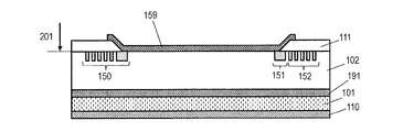
図2Aおよび図2Bは、それぞれ、本実施形態に係る半導体素子1000の概略を示す断面図および上面図である。半導体素子1000はショットキーバリアダイオードである。
2A and 2B are a cross-sectional view and a top view showing the outline of the
半導体素子1000は、第1導電型の半導体基板101と、半導体基板101の主面上に配置された、半導体層とを含む。半導体層は、前述した「所定の素子領域を有する半導体」に相当する。半導体層は、第1導電型のドリフト層102を含む。半導体層は、ドリフト層102と半導体基板101との間に配置された第1導電型のバッファ層191をさらに含んでいてもよい。ドリフト層102内には、第2導電型の終端領域150が配置されていてもよい。
The
ドリフト層102の表面201上には、第1電極159が配置されている。第1電極159は、ドリフト層102とショットキー接合を形成している。第1電極159は、ドリフト層102と接する面の縁部において、終端領域150と接していてもよい。
The
第1電極159の上には、第1電極159の上面と接するように表面電極112が配置されている。
The
半導体基板101の裏面202上には、第2電極110が配置されている。第2電極110は、半導体基板101とオーミック接合を形成している。第2電極110の下面、すなわち半導体基板101と反対側の面には裏面電極113が配置されていてもよい。
The
終端領域150は、電界緩和構造を含んでいる。ここでは、電界緩和構造として、第1電極159の一部と接する第2導電型のガードリング領域151、および、第2導電型のフローティング領域であるFLR(Field Limiting Ring)領域152を含んでいる。FLR領域152は、半導体基板101の主面の法線方向から見て、ガードリング領域151を囲み、かつ、ガードリング領域151と接触しないように配置されている。なお、終端領域150は、半導体基板101の主面の法線方向から見て、ドリフト層102の表面の一部を囲む領域を有していればよく、例示する構成に限定されない。例えば、終端領域150は、半導体素子1000の中心から外縁に向かって第2導電型の不純物濃度が変化するJTE(Junction−Termination Extension)構造を有していてもよい。
The
図示するように、ドリフト層102上には絶縁膜111が配置されていてもよい。絶縁膜111は、FLR領域152を覆い、かつ、ガードリング領域151の一部を覆っていてもよい。表面電極112の端面は、絶縁膜111上に位置していてもよい。絶縁膜111の一部の上、および、表面電極112の一部の上には、保護層(パッシベーション膜)114が配置される。保護層114は、表面電極112の上面の一部および端面を覆っている。また、表面電極112上には、保護層114と少なくとも部分的に離間した絶縁層115が配置されている。保護層114および絶縁層115は同一材料を含んでもよい。例えば、保護層114および絶縁層115は、同一の絶縁膜をパターニングすることによって形成されていてもよい。
As illustrated, an insulating
保護層114は、半導体素子1000の端部に配置されており、表面電極112の一部を露出する第1開口部114pを有している。絶縁層115は、表面電極112上であり、かつ、保護層114の第1開口部114p内に配置される。この例では、絶縁層115も、表面電極112の一部を露出する第2開口部115pを有する。このため、半導体基板101の法線方向から見たとき、表面電極112は、絶縁層115によって、内側に位置する第1領域112aと外側に位置する第2領域112bとに分断されている。表面電極112のうち、第1領域112aと第2領域112bとの間に位置し、絶縁層115に接している領域を第3領域112cとする。第1領域112aと第2領域112bとは、第3領域112cによって電気的に接続されている。
The
次いで、半導体素子1000の動作を説明する。半導体素子1000では、第2電極110に対して第1電極159に正の電圧を印加することによって、第1電極159側から第2電極110側に電流が流れる。この方向を順方向と定義する。順方向電圧とは、第2電極110よりも第1電極159が正となるように第1電極159と第2電極110との間に電圧を印加することをいう。
Next, the operation of the
<変形例>
図3Aおよび図3Bは、それぞれ、本実施形態の他の半導体素子1010の断面図および上面図である。図3Aおよび図3Bでは、図2Aおよび図2Bに示す半導体素子1000と同様の構成要素には同じ参照符号を付している。以下、半導体素子1000と同様の構成については説明を省略し、異なる点を主に説明する。
<Modification>
3A and 3B are a cross-sectional view and a top view of another
半導体素子1010は、半導体素子1000の表面電極112のうち、保護層114および絶縁層115で覆われていない領域に対し、金属層116を配置した構成を有している。金属層116は、例えば第1電極159よりも厚い金属膜であってもよい。この例では、金属層116は、表面電極112の第1領域112a上に位置する第1部分116aと、第2領域112b上に位置する第2部分116bとを含む。半導体基板101の法線方向から見たとき、第1部分116aは絶縁層115で包囲されており、第2部分116bは保護層114および絶縁層115で包囲されている。
The
半導体素子1010では、金属層116上に、金属ワイヤ、バスバーなどの金属導体が接合され得る。金属層116を形成することにより、例えばバスバーなどの金属平板を、素子表面にはんだで接合することが可能となる。金属平板を接合することで、通常の金属ワイヤを接合する場合よりも接合面積を大きくして接合部の接触抵抗を低減できる。また、金属ワイヤの代わりにバスバーを用いることで配線抵抗を低減できる。
In the
金属層116は、例えば表面電極112を金属めっきすることで形成される。金属めっきは、絶縁体である保護層114および絶縁層115上には形成されず、保護層114および絶縁層115の開口部で表面電極112が露出した領域上に選択的に成長する。
The
<半導体素子1000、1010の効果>
ここで、絶縁層を有しない比較例の半導体素子と比較して、本実施形態の半導体素子1000、1010の効果を説明する。
<Effects of the
Here, the effects of the
図22Aおよび図22Bは、それぞれ、比較例1の半導体素子9000を示す断面図および上面図である。図23Aおよび図23Bは、それぞれ、比較例2の半導体素子9010を示す断面図および上面図である。これらの図では、図2A、図2B、図3A、図3Bと同様の構成要素には同じ符号を付している。
22A and 22B are a cross-sectional view and a top view showing a
比較例1の半導体素子9000では、電界緩和構造が形成された終端領域150を覆う保護層1140は、表面電極112の周縁部を覆っており、表面電極112の一部を露出する開口部1140pを有している。開口部1140p内には、他の保護膜は形成されておらず、表面電極112の一部領域(以下、「露出領域」)1121が露出している。その他の構造は、本実施形態の半導体素子1000と同様である。
In the
比較例2の半導体素子9010は、比較例1の半導体素子9000の表面電極112上に金属層1160を配置した構成を有する。金属層1160は、保護層1140の開口部1140p内において、表面電極112の露出領域1121上に形成されている。
A
半導体素子9000の検査工程においては、検査装置の試料台上に半導体素子9000を設置し、表面電極112の露出領域1121に対して単数または複数のプローブを接触させる。特に10A以上の大電流を印加する場合は、複数のプローブを表面電極112の露出領域1121に接触させる必要がある。プローブは、露出領域1121に均等に配置されることが好ましく、保護層1140の開口部1140pの側面付近にもプローブが配置されることがある。このとき、開口部1140pの側面付近に配置されたプローブが、保護層1140を傷つける可能性がある。
In the step of inspecting the
これに対し、図2Aおよび図2Bに示す半導体素子1000の検査工程においては、絶縁層115をガイドとして用い、絶縁層115の内側の第1領域112aのみにプローブを接触させることが可能である。従って、保護層114はプローブと接触することがない。なお、絶縁層115の第2開口部115pの側面付近にもプローブが配置されることがあり、このプローブが、絶縁層115を傷つける可能性がある。しかしながら、保護層114は絶縁層115と独立に形成されているため、絶縁層115が劣化、割れ、剥離などを生じた場合でも、保護層114には影響を及ぼさない。従って、従来の半導体素子9000よりも高い信頼性を実現できる。なお、半導体素子1010においても、金属層19を形成する前に検査工程を行う場合には、上記と同様の効果が得られる。
On the other hand, in the inspection process of the
次いで、比較例1、2の半導体素子9000および9010をディスクリートのパッケージやモジュールに組み込む際の問題を説明する。
Next, a problem when the
図24Aは、比較例1の半導体素子9000を組み込んだモジュールまたはパッケージを例示する模式的な断面図である。この例では、半導体素子9000の裏面電極113は、導体(例えばはんだ)403を介して金属導体401に接合されている。半導体素子9000の表面電極112は、金属ワイヤ404によって、金属導体402に接合されている。図24Aでは1本の金属ワイヤ404のみが示されているが、複数本の金属ワイヤ404を用いてもよい。半導体素子9000および金属ワイヤ404は、封止材405で覆われている。封止材405は、例えば樹脂やゲルなどであってもよい。金属導体401、402の一部は封止材405から外部にはみ出している。ここでは、金属導体402がアノード、金属導体401がカソードとなる。
FIG. 24A is a schematic cross-sectional view illustrating a module or package incorporating the
また、図24Bは、比較例2の半導体素子9010を組み込んだモジュールまたはパッケージを例示する模式的な断面図である。この例では、半導体素子9010の裏面電極113は、導体(例えばはんだ)403を介して金属導体401に接合されている。半導体素子9010の金属層1160は、導体(例えばはんだ)406を介して金属製のバスバー407に接合されている。半導体素子9000と同様に、半導体素子9010およびバスバー407は、封止材405で覆われている。金属導体401およびバスバー407の一部は封止材405から外部にはみ出している。ここでは、バスバー407がアノード、金属導体401がカソードとなる。
Further, FIG. 24B is a schematic cross-sectional view illustrating a module or package incorporating the
半導体素子9000に対するワイヤの接合工程では、Alワイヤ、あるいは、ワイヤボンド装置のAlワイヤ射出部が保護層1140に接触し、保護層1140を傷つけることがある。半導体素子9010にバスバーを接合する際にも、同様の問題が生じ得る。この結果、保護層1140の劣化、割れ、剥離などを誘発し、半導体素子9000の長期信頼性を損ねるおそれがある。
In the step of joining the wire to the
さらに、ワイヤまたはバスバーの接合工程において、金属層1160にクラックが生じることがある。例えば、金属層1160上に金属ワイヤをボンディングする場合、接合時の超音波や加重によっては、金属ワイヤの接触部を起点としたクラックが発生する場合がある。また、バスバーなどの金属平板をはんだにて金属層1160に接合する場合においても、接合時の加重や通電時のストレス、さらには高温環境や低温環境の繰り返しによる金属疲労等のストレスによりクラックが発生する場合がある。これらのクラックは、保護層1140に悪影響を与え、結果として半導体素子9010の長期信頼性を損ねる場合がある。
Furthermore, cracks may occur in the
これに対し、本実施形態では、半導体素子1000をパッゲージ等に組み込む際に、図4Aに示すように、表面電極112のうち絶縁層115の内側の第1領域112aのみに、単数または複数のAlワイヤを接合する。あるいは、図4Bに示すように、半導体素子1010をパッゲージ等に組み込む際に、図4Bに示すように、金属層116のうち絶縁層115の内側に位置する第1部分116aのみにバスバーを接合する。このため、保護層114がワイヤ、バスバーなどと直接接触することを防止できる。また、ワイヤ、バスバーなどとの接触によって絶縁層115が劣化、割れ、剥離などを生じた場合でも、保護層114は絶縁層115と独立に形成されているため、保護層114に与える影響を低減できる。
On the other hand, in the present embodiment, when the
また、ワイヤまたはバスバーの接合工程において、金属層116にクラックが生じる場合、金属層116のうちワイヤ等が接合される第1部分116aのみにクラックが生じ得る。第1部分116aに生じたクラックは、絶縁層115および金属層116の第2部分116bを介在しているため、保護層114まで延伸しにくい。従って、ワイヤなどの接合時のクラックに起因する保護層114の長期信頼性の低下を抑制できる。
In addition, when the
さらに、半導体素子9000に対し、検査工程を実施すると、表面電極112にプローブ痕が形成される場合がある。この状態で、表面電極112上に金属層1160を配置して半導体素子9010を形成すると、次のような問題が生じ得る。
Further, when the
図25Aおよび図25Bは、それぞれ、検査工程後に金属層1160を設けることによって得られた半導体素子9010を例示する断面図および上面図である。図示するように、表面電極112には、検査工程で生じたプローブ痕901が生じており、表面に凹凸が形成されている。プローブ痕901を有する表面電極112上に金属層1160を形成すると、プローブ痕901が起点となり、金属層1160にクラック902が入る場合がある。特に、金属層1160を金属めっきで形成すると、保護層1140と金属層1160とが密接した状態となるため、クラック902が金属層1160端にまで延伸した場合には、図25Bに示すように保護層1140にもクラック903が延伸するおそれがある。または、クラック902によって想定外の応力がかかり、保護層1140が表面電極112から部分的に剥離する場合がある。保護層1140に異常が発生すると、半導体素子を樹脂等で封止していたとしても、長期的には水分やイオン等の影響を受けて保護層1140が劣化し得る。この結果、水分やイオン等の外乱が絶縁膜111にまで達し、半導体素子9000の長期信頼性を低下させる可能性がある。
25A and 25B are a cross-sectional view and a top view illustrating a
これに対し、本実施形態では、検査工程後に金属層116を形成しても上記のような問題は生じない。
On the other hand, in the present embodiment, even if the
図5Aおよび図5Bは、それぞれ、検査工程後に金属層116を形成することによって得られた半導体素子1010を例示する断面図および上面図である。
5A and 5B are a cross-sectional view and a top view illustrating a
検査工程におけるプローブ痕901は、絶縁層115の第2開口部内に位置する第1領域112aにのみ形成される。第2領域112bにはプローブが接触しないため、プローブ痕901は形成されない。この表面電極112上に、例えば金属めっきにより金属層116を形成すると、プローブ痕901が起点となり、金属層116の第1部分116aにクラック902が入る場合がある。特に、金属層116を金属めっきで形成する場合には、保護層114、絶縁層115および金属層116の第1部分116a、第2部分116bが密接した状態となっている。このため、クラック902が金属層116の第1部分116a端にまで延伸した場合には、図5Bに示すように、絶縁層115にもクラック903が生じるおそれがある。または、クラック902によって想定外の応力がかかり、絶縁層115が表面電極112から部分的に剥離する場合がある。このように絶縁層115に異常が発生すると、半導体素子1010を樹脂等で封止していたとしても、長期的には水分やイオン等の影響を受けて絶縁層115が劣化する場合がある。
The
しかしながら、本実施形態では、絶縁層115は保護層114と離間しており、その間に金属層116が介在しているため、絶縁層115に生じたクラック903が、金属層116の第2部分116bを超えて保護層114まで延伸することが抑制される。従って、クラック902、903に起因する保護層114の機能低下を抑制できるので、長期信頼性を確保できる。
However, in the present embodiment, the insulating
(半導体素子1000および1010の製造方法)
図6から図16を参照しながら、本実施形態に係る半導体素子1000および1010の製造方法を説明する。図6から図16は、それぞれ、半導体素子1000および1010の製造方法を説明するための工程断面図である。
(Method of
A method of manufacturing the
まず、半導体基板101を準備する。半導体基板101は、例えば、抵抗率が0.02Ωcm程度である低抵抗のn型4H−SiCオフカット基板である。
First, the
図6に示すように、半導体基板101の上に高抵抗でn型のドリフト層102をエピタキシャル成長により形成する。ドリフト層102を形成する前に、半導体基板101上に、n型で高不純物濃度のSiCによって構成されるバッファ層191を堆積してもよい。バッファ層191の不純物濃度は、例えば、1×1018cm−3であり、バッファ層191の厚さは例えば0.5μmである。ドリフト層102は、例えば、n型4H−SiCによって構成される。ドリフト層102の不純物濃度及び厚さは、例えば、それぞれ、1.0×1016cm−3及び10μmである。
As shown in FIG. 6, a high-resistance n-
次に、図7に示すように、ドリフト層102の上に、例えばSiO2からなるマスク501を形成した後、Alイオンなどのp型の不純物イオンをドリフト層102に注入する。これにより、ドリフト層102に、ガードリング注入領域1510およびFLR注入領域1520を含む終端注入領域1500が形成される。終端注入領域1500、ガードリング注入領域1510およびFLR注入領域1520は、それぞれ、後に、終端領域150、ガードリング領域151およびFLR領域152となる。終端注入領域1500、ガードリング注入領域1510およびFLR注入領域1520の注入ドーズ量はいずれも4.6×1015cm−2であり、不純物注入時には半導体基板101は例えば300℃以上500℃以下に加熱されていてもよい。このとき、終端領域150とドリフト層102の間に形成されるpn接合までの接合深さが、ドリフト層102の表面201から例えば1μm程度になるように不純物注入エネルギーが調整される。不純物注入後、マスク501は除去される。
Next, as shown in FIG. 7, after forming a
次に、図8に示すように、1500℃以上1900℃以下の温度で熱処理することにより、終端注入領域1500、ガードリング注入領域1510、FLR注入領域1520から、それぞれ、終端領域150、ガードリング領域151、FLR領域152が形成される。なお、熱処理実施前にドリフト層102の表面にカーボン膜を堆積し、熱処理後にカーボン膜を除去してもよい。また、その後に、ドリフト層102の少なくとも表面201に熱酸化膜を形成後、その熱酸化膜をエッチングで除去することにより、ドリフト層102の表面201を清浄化してもよい。
Next, as shown in FIG. 8, by performing heat treatment at a temperature of 1500° C. or higher and 1900° C. or lower, the
次に、図9に示すように、半導体基板101の裏面202側に、例えばニッケル(Ni)を200nm程度堆積した後、800℃以上1050℃以下で熱処理することにより第2電極110を形成する。第2電極110は半導体基板101の裏面202とオーミック接合を形成する。ここでは電極材料としてNiを選択したが、半導体基板101と反応することによりシリサイドまたはカーバイドを形成できる金属を含んでいれば他の金属であってもよい。選択した金属材料により個別に熱処理温度を選択してもよい。また、オーミック接合が実現できるのであれば、熱処理温度は、例えば200℃以上600℃以下であってもよい。
Next, as shown in FIG. 9, for example, nickel (Ni) is deposited to a thickness of about 200 nm on the
次に、ドリフト層102表面に例えばSiO2からなる絶縁膜を形成する。絶縁膜の厚さは例えば300nmである。次にフォトレジストによるマスクを形成して例えばウェットエッチングによりガードリング領域151の一部、および、ガードリング領域151の内側のドリフト層102を露出させる。その後マスクを除去する。このようにして、図10に示すように、開口を有する絶縁膜111が得られる。
Next, an insulating film made of, for example, SiO 2 is formed on the surface of the
次に、開口を有する絶縁膜111および開口に露出したドリフト層102の全面を覆うように、第1電極用導電膜が堆積される。第1電極用導電膜は例えば、Ti、Ni、Mo等である。第1電極用導電膜の厚さは例えば200nmである。この後フォトレジストによるマスクを形成して、少なくとも絶縁膜111から露出したドリフト層102を覆う部分が残るように第1電極用導電膜をパターニングする。これにより、図11に示すように、第1電極159が得られる。図11の例では、第1電極159の端部は絶縁膜111上にある。第1電極159は、暴露されたドリフト層102、およびガードリング領域151の一部と接している。その後、第1電極159を有する半導体基板101を100℃以上700℃以下の温度で熱処理する。これにより、第1電極159は、ドリフト層102とショットキー接合を形成する。
Next, the conductive film for the first electrode is deposited so as to cover the entire surface of the insulating
次に、第1電極159および絶縁膜111の上方に表面電極用導電膜を堆積する。表面電極用導電膜は、例えばAlを含む4μm程度の金属膜である。表面電極用導電膜上にマスクを形成して不要な部分をエッチングすることで絶縁膜111の一部を露出させる。表面電極用導電膜をウェットエッチングする際には、第1電極159が露出しないように表面電極用導電膜のエッチング条件を調整してもよい。表面電極用導電膜の一部をエッチングした後にマスクを除去することで、図12に示すような表面電極112が形成される。
Next, a conductive film for a surface electrode is deposited above the
次に、図13に示したように保護層114を形成する。まず、露出した絶縁膜111および表面電極112の上方に、保護層114として、例えばSiN等の無機保護膜またはポリイミド等の有機保護膜を形成する。その後、表面電極112の上部に形成された保護層114が暴露するような開口を有するマスクを準備し、例えばドライエッチングやフォトリソ工程により保護層114の一部をエッチングして、表面電極112の一部を露出させる第1開口部114pを形成する。その後、マスクを除去する。保護層114は、絶縁体であれば他の無機保護膜(例えばSiO2)や他の有機保護膜(例えばポリベンゾオキサゾール)あってもよい。
Next, the
次に、図14に示したように絶縁層115を形成する。まず、露出した表面電極112および保護層114の上方に、絶縁層115として例えばSiNやSiO2等の無機絶縁膜またはポリイミド等の有機絶縁膜を形成する。その後、表面電極112の上部に形成された絶縁層115が暴露するような開口を有するマスクを準備し、例えばドライエッチングやフォトリソ工程により絶縁層115の一部をエッチングして、表面電極112の一部を露出させる第2開口部115pを形成する。その後、マスクを除去する。第2開口部115pは、保護層114の第1開口部114pの内側に配置される。絶縁層115は絶縁体であれば他の無機絶縁膜(例えばSiO2)や他の有機絶縁膜(例えばポリベンゾオキサゾール)あってもよいが、絶縁層115のエッチングの際に、保護層114ができるだけダメージを受けないよう、保護層114と絶縁層115は異なる材料を選択することが好ましい。表面電極112の露出された領域のうち第2開口部115pで包囲された領域は第1領域112a、保護層114と絶縁層115との間に位置する領域は第2領域112bとなる。
Next, the insulating
ここで、保護層114および絶縁層115の厚さは、例えば0.3〜10μm程度である。また、絶縁層115の半導体素子1000および1010の面内方向の幅は、例えば5〜500μm程度である。さらに、保護層114および絶縁層115の間隔は、例えば5〜50μm程度である。
Here, the thickness of the
一方で、保護層114および絶縁層115を同じ材料で同時に形成してもよい。この場合は半導体素子作製工程の簡略化が可能となる。図13の構造に対し、まず、露出した絶縁膜111および表面電極112の上方に、絶縁膜(例えばSiNなどの無機絶縁膜またはポリイミド等の有機絶縁膜)を形成する。その後、絶縁膜が複数領域で暴露するような開口を有するマスクを準備し、例えばドライエッチングやフォトリソ工程により絶縁膜の一部をエッチングして表面電極112の一部を露出させる。ここでは、絶縁膜に、第2開口部115pと、その外側に位置する環状の開口部とを形成する。このようにして、絶縁膜から、保護層114および絶縁層115が同時に形成される。その後、マスクを除去する。保護層114は絶縁体であれば他の無機保護膜(例えばSiO2)や他の有機保護膜(例えばポリベンゾオキサゾール)あってもよい。
On the other hand, the
次に、図15に示すように、必要に応じて裏面電極113が形成される。裏面電極113の形成プロセスは、上記の保護層114、絶縁層115の形成工程の前であってもよいし、表面電極112の形成工程の前であってもよい。裏面電極113は、例えば、第2電極110に接する側から、Ti、Ni、Agの順に堆積する。Ti、Ni、Agの厚さはそれぞれ、例えば0.1μm、0.3μm、0.7μmである。以上の工程を経て、半導体素子1000が形成される。
Next, as shown in FIG. 15, the
さらに、図16に示すように、半導体素子1000に対して、表面に金属層116を形成することで半導体素子1010が得られる。金属層116は、例えば次のようにして形成される。まず半導体素子1000の裏面電極113が暴露しないよう、テープ等で保護する。次に、保護層114、絶縁層115で覆われていない表面電極112に対し、めっきしやすいよう表面処理を施し、めっき液に浸すことで表面電極112上に金属層116を形成する。このとき、絶縁膜である保護層114、絶縁層115上にはめっきされず、暴露された表面電極112上に選択的に成長する。従って、金属層116は、第1領域112a上および第2領域112b上に形成される。金属層116のうち第1領域112a上に形成された第1部分116aと、第2領域112b上に形成された第2部分116bとは、絶縁層115によって分離されている。ここでは、無電解めっきとして、例えばNiを主成分とする金属膜を3〜10μm程度めっきして、金属層116を形成する。金属層116の厚さは、保護層114および絶縁層115の厚さよりも小さくてもよい。Niを主とする金属層116は、例えばAlを主とする表面電極112に比べて硬いため、表面電極112に外部電極との電気的接合を形成する場合に比べてクラックが発生しやすくなる。しかし、図16で示したように、金属層116は、絶縁層115によって、第1部分116aと第2部分116bに分割されており、絶縁層115は保護層114と離間している。したがって、第1部分116aにクラックが発生し、チップ外側へ延伸したとしても、絶縁層115と金属層116の第2部分116bとが介在することにより保護層114へクラックが延伸することはなく、保護層114の機能を損ねることはないので、結果として半導体素子1010の長期信頼性に悪影響を与えない。
Furthermore, as shown in FIG. 16, a
なお、上記例では無電解めっきで説明したが、電解めっきで金属層116を形成してもよい。また、その他の方法(蒸着やスパッタなど)で金属層116を形成してもよい。但しこの場合は、別途エッチング工程を追加するなどして、金属層116を、2つの部分116a、116bに分離することが好ましい。
In the above example, the electroless plating is described, but the
(第2の実施形態)
以下、図面を参照しながら、本開示の半導体素子の第2の実施形態を説明する。本実施形態の半導体素子は、複数の表面電極を備える。以下、SiCを用いた縦型MISFETを例に、本実施形態の半導体素子の構成を説明する。
(Second embodiment)
Hereinafter, a second embodiment of the semiconductor device of the present disclosure will be described with reference to the drawings. The semiconductor device of this embodiment includes a plurality of surface electrodes. Hereinafter, the configuration of the semiconductor element of the present embodiment will be described by taking a vertical MISFET using SiC as an example.
図17Aは、本実施形態の半導体素子2000の平面図であり、図17Bは、図17Aに示すA−A’線における半導体素子2000の断面図である。
17A is a plan view of the
半導体素子2000は、第1導電型の炭化珪素基板301と、炭化珪素基板301の主面に位置する第1炭化珪素半導体層(ドリフト層)302とを備える。第1炭化珪素半導体層は、前述した「所定の素子領域を有する半導体」に相当する。炭化珪素基板301の裏面にはドレイン電極310およびドレイン電極310上に配置された裏面電極(配線電極)320が位置している。本実施形態では、第1導電型はn型であり、第2導電型はp型である。しかし、第1導電型がp型であり、第2導電型はn型であってもよい。
炭化珪素基板301は、活性領域300Aと、終端領域300Eとを含む。炭化珪素基板301の主面に垂直な方向から見たとき、終端領域300Eは活性領域300Aを囲んでいる。
半導体素子2000は、活性領域300Aに位置する複数のユニットセル300uを含む。複数のユニットセル300uのそれぞれは、MISFETとして機能し、互いに並列に接続されている。つまり、ユニットセル300uにおいて、トランジスタが構成されており、半導体素子2000は複数のトランジスタを含む。炭化珪素基板301の主面に垂直な方向からみて、複数のユニットセル300uは、2次元に配列されている。
The
各ユニットセル300uは、第1導電型の炭化珪素基板301と、炭化珪素基板301上に位置する第1導電型の第1炭化珪素半導体層302と、第1炭化珪素半導体層302の表面に選択的に形成された第2導電型の第1ボディ領域303と、第1ボディ領域303の表面に選択的に形成されたソース領域304と、第1炭化珪素半導体層302の上方に位置するゲート絶縁膜307と、ゲート絶縁膜307上に位置するゲート電極308とを備えている。第1炭化珪素半導体層302とゲート絶縁膜307との間にチャネル層として第2炭化珪素半導体層306が設けられていてもよい。
Each
第1炭化珪素半導体層302において、ソース領域304は、高濃度で第1導電型の不純物を含む(n+型)。第1ボディ領域303への電気的接続のため、第1ボディ領域303よりも高い濃度で第2導電型の不純物を含む第2導電型の第1コンタクト領域305がソース領域304内であって、ソース領域304の下方で第1ボディ領域303と接する位置に設けられている。また、第1炭化珪素半導体層302の表面には、ソース領域304および第1コンタクト領域305とオーミック接合によって電気的に接続されたソース電極309が設けられている。従って、第1ボディ領域303は、第1コンタクト領域305を介してソース電極309と電気的に接続される。
In first silicon
第1ボディ領域303、ソース領域304および第1コンタクト領域305は、例えば、第1炭化珪素半導体層302に対して不純物を注入する工程と、第1炭化珪素半導体層302に注入された不純物を活性化させる高温熱処理(活性化アニール)工程とによって形成される。ソース電極309は、例えば、第1炭化珪素半導体層302におけるソース領域304および第1コンタクト領域305の上に例えば導電材料(Ni)層を形成した後、高温で熱処理することによって形成できる。
The
ソース領域304と第1炭化珪素半導体層302とは、第2炭化珪素半導体層306を介して接続されている。第2炭化珪素半導体層306は、例えば、エピタキシャル成長によって第1炭化珪素半導体層302の上に形成された4H−SiC層であり、第1導電型の不純物がドープされている。第2炭化珪素半導体層306の厚さは例えば75nm以下であり、かつ、ドーピング濃度は1×1018cm−3以上であってもよい。第2炭化珪素半導体層306は後述する終端領域のFLR領域上には設けられていなくてもよい。
ソース領域304および第1コンタクト領域305は、それぞれ、ソース電極309とオーミック接触を形成している。半導体素子2000が第2炭化珪素半導体層306を備えていない場合には、ゲート電圧を印加することにより、第1ボディ領域303の表面近傍にチャネルとなる反転層を形成させてトランジスタを動作させることができる。
The
ゲート絶縁膜307は、例えば、第2炭化珪素半導体層306の表面を熱酸化することによって形成された熱酸化膜(SiO2膜)である。ゲート電極308は、例えば導電性のポリシリコンを用いて形成されている。
The
層間絶縁膜311は、活性領域300Aおよび終端領域300Eにおけるゲート電極308、終端領域300Eにおけるゲート絶縁膜307等を覆って第1炭化珪素半導体層302または第2炭化珪素半導体層306上に位置している。このため、ゲート電極308は、層間絶縁膜311によって覆われている。
層間絶縁膜311には開口部が形成されており、各ユニットセルにおけるソース電極309は、この開口部を介して、第1表面電極(例えばAl電極)312に並列に接続されている。第1表面電極312は、半導体素子2000において複数形成されたMISFETのユニットセルにおけるソース電極を並列接続している。
An opening is formed in the
半導体素子2000は、終端領域300Eにおいて、終端構造を有する。終端構造は、終端領域300Eにおいて、炭化珪素基板301と、炭化珪素基板301の主面に位置する第1炭化珪素半導体層302とを備える。また、終端構造は、第1炭化珪素半導体層302の表面に選択的に形成され、活性領域300Aを囲む第2導電型の第2ボディ領域325と、第2ボディ領域325の表面に選択的に形成された第2導電型の第2コンタクト領域326とを含む。第2コンタクト領域326も第2ボディ領域325と同様、活性領域300Aを囲んでいる。第2ボディ領域325は、深さ方向において、第1ボディ領域303と同じ不純物濃度プロファイルを有してもよい。同様に、第2コンタクト領域326は、深さ方向において、第1コンタクト領域305と、同じ不純物濃度プロファイルを有してもよい。つまり、第2ボディ領域325は第1ボディ領域303と同じ工程によって形成してもよく、第2コンタクト領域326は第1コンタクト領域305と同じ工程によって形成してもよい。
The
終端構造は、複数のベース電極(第1ベース電極)319aおよびベース電極(第2ベース電極)319b、319cを備えてもよい。ベース電極319a、319b、319cは、第2コンタクト領域326と接触するように第1炭化珪素半導体層302の表面に形成されている。ベース電極319aは、終端領域300Eの第2コンタクト領域326のうち、活性領域300Aに近接する内周側(図の左側)の領域に位置している。ベース電極319aは、島状に形成されており、例えば、活性領域300Aにおけるソース電極309と同様に配列されている。一方、ベース電極319b、319cは、後述するゲート電極308の外周縁よりも外側であって、第2コンタクト領域326の外周側(図の右側)の領域に位置し、活性領域300Aを囲む。つまり、炭化珪素基板301の主面に垂直な方向からみて環形状を有している。環形状のベース電極は1つであってもよいし、3以上であってもよい。ベース電極319a、319b、319cは、層間絶縁膜311の開口部を介して、第1表面電極312に接続されている。
The termination structure may include a plurality of base electrodes (first base electrodes) 319a and base electrodes (second base electrodes) 319b and 319c.
終端領域300Eにおいて、第1炭化珪素半導体層302の上には第2炭化珪素半導体層306と、ゲート絶縁膜307とが位置している。また、終端領域300Eにおいて、上部ゲート電極を設けるため、ゲート電極308もゲート絶縁膜307上に位置していてもよい。ゲート電極308は、層間絶縁膜311の開口部を介して、第2表面電極(例えばAl電極)313に接続されている。第2表面電極313は、複数のMISFETのゲート電極308にゲート信号を与える役割を有している。第2表面電極313および第1表面電極312は、同一の導電膜をパターニングすることにより同時に形成され得る。
In
終端構造は、第1炭化珪素半導体層302の表面に位置し、第2ボディ領域325を囲むFLR領域において、少なくとも1つの第2導電型のリング領域352を有する。リング領域352は、深さ方向において、活性領域300Aの第1ボディ領域303及び第2ボディ領域325と同一の不純物濃度プロファイルを有してもよい。
The termination structure is located on the surface of first silicon
半導体素子2000における終端領域300Eおよび活性領域300Aには、内部の構造を外部の環境から保護するため、保護層314が形成されている。保護層314は、第1表面電極312および第2表面電極313の上方に配置されており、これらの表面電極の一部を露出する第1開口部314pを有している。第1表面電極312および第2表面電極のうち保護層314から露出した領域が、それぞれ、ソースパッド領域SP、ゲートパッド領域GPとなる。なお、この例では、第1表面電極312を露出する第1開口部314pが2つ設けられ、2つのソースパッド領域SPが形成されている。
A
ソースパッド領域SPにおいて、保護層314の第1開口部314p内に第1絶縁層315が配置されている。第1絶縁層315は、保護層314と離間して配置されており、第1表面電極312の一部を露出する第2開口部315pを有している。ゲートパッド領域GPにおいても、同様に、保護層314の第1開口部314p内に第2絶縁層316が配置されている。第2絶縁層316は、保護層314と離間して配置されており、第2表面電極313の一部を露出する第2開口部316pを有している。
In the source pad region SP, the first insulating
図17Bに示すように、保護層314は、活性領域300Aおよび終端領域300Eにおいて、ソースパッド領域SPおよびゲートパッド領域GPを除いて、第1表面電極312および第2表面電極313の全体を覆っていてもよい。パッド領域とは、パッケージの端子に接続するために、ワイヤやリボンやバスバーなどを接続する領域であり、表面電極が露出されている領域である。この例では、2つのソースパッド領域SPおよび1つのゲートパッド領域GPが設けられている。なお、パッド領域の数および配置は、図示する例に限定されない。
As shown in FIG. 17B, the
図17Aから分かるように、半導体素子2000を上方から見たとき、ソースパッド領域SPにおいて、第1表面電極312の一部が露出している。第1表面電極312の露出部分は、第1絶縁層315の第2開口部内に位置する第1領域312aと、保護層314と第1絶縁層315との間に位置する第2領域312bとを含む。すなわち、第1表面電極312は第1絶縁層315で領域を分割されており、内側が第1領域312a、外側が第2領域312bである。
As can be seen from FIG. 17A, when the
同様に、ゲートパッド領域GPにおいて、第2表面電極313の一部が露出している。第2表面電極313の露出部分は、第2絶縁層316の第2開口部内に位置する第1領域313aと、保護層314と第2絶縁層316との間に位置する第2領域313bとを含む。すなわち、第2表面電極313は第2絶縁層316で領域を分割されており、内側が第1領域313a、外側が第2領域313bである。
Similarly, in the gate pad region GP, a part of the
本実施形態でも、半導体素子1000と同様に、第1表面電極312、第2表面電極313における絶縁層115の第2開口部内に位置する第1領域312a、313aで、それぞれ、ソースおよびゲートの信号を与えるためのプローブやワイヤを接触させる。これにより、プローブまたはワイヤが位置ずれによって第1および第2絶縁層315、316に接触したとしても、保護層314とこれらの絶縁層とが離間しているため、保護層314への悪影響を低減でき、長期信頼性の低下を抑制できる。
Also in the present embodiment, similarly to the
ソースパッド領域SPおよびゲートパッド領域GPの配置および構成は、図17Aに示す例に限定されない。 The arrangement and configuration of the source pad region SP and the gate pad region GP are not limited to the example shown in FIG. 17A.
図18〜図21は、本実施形態の他の半導体素子2010、2011、2020、2021を示す平面図である。
18 to 21 are plan views showing
図18に示すように、ソースパッド領域SPおよびゲートパッド領域GPは、それぞれ、1つずつ設けられていてもよい。 As shown in FIG. 18, one source pad region SP and one gate pad region GP may be provided.
図19に示すように、図18に示す半導体素子2010における第1表面電極312、第2表面電極313の露出部分上に、それぞれ、第1金属層317および第2金属層318が配置されていてもよい。第1金属層317のうち第1領域312a上に位置する部分を第1部分317a、第2領域312b上に位置する部分を第2部分317bとし、第2金属層318のうち第1領域313a上に位置する部分を第1部分318a、第2領域313b上に位置する部分を第2部分318bとする。第1金属層317、318は、前述に実施形態における金属層116と同様の方法で形成され得る。第1金属層317、318は、検査工程の前に形成されてもよいし、検査工程後に形成されてもよい。
As shown in FIG. 19, the
また、複数の表面電極を有する半導体素子では、複数の表面電極の一部のみに絶縁層を設けてもよい。例えば、第1表面電極312、第2表面電極313のいずれか一方に特にクラックが発生しやすい場合には、クラックが発生しやすい方にのみ絶縁層を設けてもよい。図20に例示するように、ゲートパッド領域GPにおいて、第2表面電極313上に第2絶縁層316を配置し、ソースパッド領域SPでは、第1表面電極312上には絶縁層を配置しなくてもよい。
Further, in a semiconductor element having a plurality of surface electrodes, an insulating layer may be provided only on a part of the plurality of surface electrodes. For example, when a crack is particularly likely to occur on either the
さらに、図21に例示するように、図20に示す半導体素子2020において、第1表面電極312、第2表面電極313の露出部分上に第1金属層317、318を形成してもよい。
Further, as illustrated in FIG. 21, in the
なお、図20および図21に示す例では、ゲートパッド側にのみ絶縁層を配置したが、ソースパッド側にのみ絶縁層を配置してもよい。 Although the insulating layer is arranged only on the gate pad side in the example shown in FIGS. 20 and 21, the insulating layer may be arranged only on the source pad side.
さらに、インテリジェント化(具体的には、半導体素子上に温度センサや電流センサを搭載して多機能化)した半導体素子では、ゲートパッド、ソースパッド以外にも信号を取り出すための電極パッドが必要になり、3以上の表面電極が配置される場合がある。このような場合でも、全ての表面電極上において、保護層の開口部内に絶縁層を配置してもよいし、一部の表面電極上にのみ絶縁層を配置してもよい。 In addition, intelligent semiconductor devices (specifically, semiconductor devices with temperature sensors and current sensors mounted on them to make them multifunctional) require electrode pads for extracting signals in addition to gate pads and source pads. In some cases, three or more surface electrodes are arranged. Even in such a case, the insulating layer may be arranged in the openings of the protective layer on all the surface electrodes, or the insulating layer may be arranged only on a part of the surface electrodes.
本開示の半導体素子の構成および各構成要素の材料は、上記に例示した構成および材料に限定されない。上記の実施形態では、炭化珪素が4H−SiCである例について説明したが、炭化珪素は6H−SiC、3C−SiC、15R−SiCなどの他のポリタイプであってもよい。また、本開示の実施形態では、SiC基板の主面が(0001)面からオフカットした面である例について説明したが、SiC基板の主面は、(11−20)面、(1−100)面、(000−1)面、またはこれらのオフカット面であってもよいし、その他の特殊な面方位であってもよい。また、炭化珪素基板301の代わりにSi基板を用い、Si基板上に、3C−SiCのドリフト層を形成してもよい。
The configuration of the semiconductor element of the present disclosure and the material of each component are not limited to the configurations and materials illustrated above. In the above embodiment, an example in which the silicon carbide is 4H-SiC has been described, but the silicon carbide may be another polytype such as 6H-SiC, 3C-SiC, 15R-SiC. Further, in the embodiment of the present disclosure, an example in which the main surface of the SiC substrate is a surface that is off-cut from the (0001) plane has been described, but the main surface of the SiC substrate is the (11-20) plane and the (1-100) plane. ) Plane, (000-1) plane, or off-cut planes thereof, or other special plane orientations. A Si substrate may be used instead of
さらに、本開示の半導体素子は、炭化珪素以外の他の半導体を用いた半導体素子であってもよい。他の半導体は、例えば、窒化ガリウム(GaN)、窒化アルミニウム(AlN)等の他のワイドバンドギャップ半導体であってもよいし、シリコン半導体であってもよい。 Furthermore, the semiconductor element of the present disclosure may be a semiconductor element using a semiconductor other than silicon carbide. The other semiconductor may be another wide band gap semiconductor such as gallium nitride (GaN) or aluminum nitride (AlN), or may be a silicon semiconductor.
なお、上記の実施形態においては、表面電極を備えた半導体素子としてSBDおよびMISFETを例示したが、本開示の構成は他の半導体素子にも適用できる。特に、高耐圧を実現するためのパワー素子に好適に適用され得る。 Although the SBD and the MISFET are exemplified as the semiconductor element having the surface electrode in the above-described embodiment, the configuration of the present disclosure can be applied to other semiconductor elements. In particular, it can be suitably applied to a power element for realizing a high breakdown voltage.
例えば、図17Aおよび図17Bに示す半導体素子2000において、基板とその上に形成する半導体層(ドリフト領域)とを互いに異なる導電型とすることにより、絶縁ゲートバイポーラトランジスタ(IGBT)を形成することができる。IGBTの場合、上述したトレンチ型MISFETにおけるソース電極、ドレイン電極及びソース領域は、それぞれ順に、エミッタ電極、コレクタ電極及びエミッタ領域と呼ばれる。ドリフト領域及びエミッタ領域の導電型をn型とし、基板及びボディ領域の導電型をp型とすると、n型チャネルのIGBTを得ることができる。また、ドリフト領域及びエミッタ領域の導電型をp型とし、基板及びボディ領域の導電型をn型とすると、p型チャネルのIGBTを得ることができる。
For example, in the
本開示は、例えば、民生用、車載用、産業機器用等の電力変換器に搭載されるパワー半導体デバイスに用いられ得る。 The present disclosure can be used for, for example, a power semiconductor device mounted on a power converter for consumer use, vehicle installation, industrial equipment, or the like.
10、1000、1010、2000、2010、2011、2020、2021 :半導体素子
11 :半導体
13、112、312、313 :表面電極
13a、112a、312a、313a :第1領域
13b、112b、312b、313b :第2領域
15、114、314 :保護層
15p、114p、314p :第1開口部
17、115、315、316 :絶縁層
17p、115p、315p :第2開口部
19、116、317、318 :金属層
19a、116a、317a、318a :第1部分
19b、116b、317b、318b :第2部分
101 :半導体基板
102 :ドリフト層
110 :第2電極
111 :絶縁膜
113 :裏面電極
150、300E :終端領域
151 :ガードリング領域
152 :FLR領域
159 :第1電極
191 :バッファ層
301 :炭化珪素基板
302 :第1炭化珪素半導体層
303 :第1ボディ領域
304 :ソース領域
305 :第1コンタクト領域
306 :第2炭化珪素半導体層
307 :ゲート絶縁膜
308 :ゲート電極
309 :ソース電極
310 :ドレイン電極
311 :層間絶縁膜
401、402、407 :金属導体
403、406 :はんだ
404 :金属ワイヤ
405 :封止材
GP :ゲートパッド領域
SP :ソースパッド領域
10, 1000, 1010, 2000, 2010, 2011, 2020, 2021: semiconductor element 11:
Claims (13)
前記素子領域の端部において、前記半導体に配置された電界緩和構造と、
前記半導体の上に配置され、かつ、前記半導体の法線方向から見たとき、前記電界緩和構造の内側に位置する、少なくとも1つの表面電極と、
前記電界緩和構造と前記少なくとも1つの表面電極の周縁部とを覆い、かつ、前記少なくとも1つの表面電極上に開口部を有する保護層と、
前記少なくとも1つの表面電極上において、前記開口部の内側に、前記保護層と離間し、かつ、前記半導体の法線方向から見たとき、前記少なくとも1つの表面電極の第1領域を包囲するように配置された絶縁層と、
前記少なくとも1つの表面電極のうち前記保護層および前記絶縁層のいずれにも覆われていない領域上に配置された金属層と
を備え、
前記金属層は、少なくとも前記第1領域上に配置されている、半導体素子。 A semiconductor having a predetermined element region,
An electric field relaxation structure disposed in the semiconductor at an end of the element region,
At least one surface electrode disposed on the semiconductor and located inside the electric field relaxation structure when viewed from a direction normal to the semiconductor;
A protective layer that covers the electric field relaxation structure and a peripheral portion of the at least one surface electrode, and has an opening on the at least one surface electrode;
On the at least one surface electrode, spaced apart from the protective layer inside the opening , and surrounding the first region of the at least one surface electrode when viewed from the normal direction of the semiconductor. an insulating layer disposed on,
A metal layer disposed on a region of the at least one surface electrode that is not covered by either the protective layer or the insulating layer ,
The semiconductor element , wherein the metal layer is arranged at least on the first region .
前記少なくとも1つの表面電極は、カソードおよびアノードの少なくとも一方を含む、請求項1または2に記載の半導体素子。 The semiconductor element is a diode,
The semiconductor device according to claim 1, wherein the at least one surface electrode includes at least one of a cathode and an anode.
前記少なくとも1つの表面電極は、ソースおよびドレインの少なくとも一方を含む、請求項1または2に記載の半導体素子。 The semiconductor element is a transistor,
The semiconductor device according to claim 1, wherein the at least one surface electrode includes at least one of a source and a drain.
前記少なくとも1つの表面電極は、エミッタおよびコレクタの少なくとも一方を含む、請求項1または2に記載の半導体素子。 The semiconductor element is a transistor,
The semiconductor device according to claim 1, wherein the at least one surface electrode includes at least one of an emitter and a collector.
前記少なくとも1つの表面電極は、ゲートを含む、請求項1または2に記載の半導体素子。 The semiconductor element is a transistor,
The semiconductor device according to claim 1, wherein the at least one surface electrode includes a gate.
前記金属層は、前記第1領域上に位置する第1部分と、前記第2領域上に位置する第2部分とを含む、請求項1から7のいずれかに記載の半導体素子。 Wherein the at least one surface electrode, when viewed from the normal direction of the semiconductor, and the insulating layer the first region surrounded by a second region located between the protective layer and the insulating layer Including,
The semiconductor element according to claim 1, wherein the metal layer includes a first portion located on the first region and a second portion located on the second region.
Priority Applications (2)
| Application Number | Priority Date | Filing Date | Title |
|---|---|---|---|
| JP2016245590A JP6719090B2 (en) | 2016-12-19 | 2016-12-19 | Semiconductor element |
| US15/834,035 US10276470B2 (en) | 2016-12-19 | 2017-12-06 | Semiconductor device having an electric field relaxation structure |
Applications Claiming Priority (1)
| Application Number | Priority Date | Filing Date | Title |
|---|---|---|---|
| JP2016245590A JP6719090B2 (en) | 2016-12-19 | 2016-12-19 | Semiconductor element |
Publications (2)
| Publication Number | Publication Date |
|---|---|
| JP2018101662A JP2018101662A (en) | 2018-06-28 |
| JP6719090B2 true JP6719090B2 (en) | 2020-07-08 |
Family
ID=62556946
Family Applications (1)
| Application Number | Title | Priority Date | Filing Date |
|---|---|---|---|
| JP2016245590A Active JP6719090B2 (en) | 2016-12-19 | 2016-12-19 | Semiconductor element |
Country Status (2)
| Country | Link |
|---|---|
| US (1) | US10276470B2 (en) |
| JP (1) | JP6719090B2 (en) |
Families Citing this family (12)
| Publication number | Priority date | Publication date | Assignee | Title |
|---|---|---|---|---|
| US10461049B2 (en) * | 2015-12-14 | 2019-10-29 | Mitsubishi Electric Corporation | Semiconductor device and manufacturing method therefor |
| CN110199396B (en) * | 2017-01-26 | 2022-06-24 | 三菱电机株式会社 | Method for manufacturing semiconductor device |
| JP7085959B2 (en) * | 2018-10-22 | 2022-06-17 | 三菱電機株式会社 | Semiconductor equipment |
| US11538769B2 (en) | 2018-12-14 | 2022-12-27 | General Electric Company | High voltage semiconductor devices having improved electric field suppression |
| US10892237B2 (en) * | 2018-12-14 | 2021-01-12 | General Electric Company | Methods of fabricating high voltage semiconductor devices having improved electric field suppression |
| GB201909588D0 (en) * | 2019-07-03 | 2019-08-14 | Univ Coventry | A semiconductor device and methods for production thereof |
| DE212021000204U1 (en) * | 2020-06-26 | 2022-01-24 | Rohm Co., Ltd. | electronic component |
| JP2022007763A (en) * | 2020-06-26 | 2022-01-13 | 株式会社デンソー | Semiconductor device and manufacturing method for same |
| CN113540229B (en) * | 2021-06-11 | 2022-07-12 | 中兴通讯股份有限公司 | Semiconductor device and method for manufacturing the same |
| DE112022003512T5 (en) * | 2021-09-03 | 2024-05-02 | Rohm Co., Ltd. | SEMICONDUCTOR COMPONENT |
| IT202200006485A1 (en) * | 2022-04-01 | 2023-10-01 | St Microelectronics Srl | ELECTRONIC DEVICE WITH REDUCED SWITCHING OSCILLATIONS |
| JP2024015665A (en) * | 2022-07-25 | 2024-02-06 | 株式会社デンソー | Semiconductor device |
Family Cites Families (23)
| Publication number | Priority date | Publication date | Assignee | Title |
|---|---|---|---|---|
| JP2006005166A (en) * | 2004-06-17 | 2006-01-05 | Matsushita Electric Ind Co Ltd | Manufacturing method of semiconductor device |
| US7183626B2 (en) * | 2004-11-17 | 2007-02-27 | International Rectifier Corporation | Passivation structure with voltage equalizing loops |
| JP5048273B2 (en) * | 2006-05-10 | 2012-10-17 | オンセミコンダクター・トレーディング・リミテッド | Insulated gate semiconductor device |
| JP4189415B2 (en) * | 2006-06-30 | 2008-12-03 | 株式会社東芝 | Semiconductor device |
| JP4356764B2 (en) * | 2007-04-18 | 2009-11-04 | 株式会社デンソー | Silicon carbide semiconductor device |
| US20090050899A1 (en) * | 2007-08-23 | 2009-02-26 | National Institute of Advanced Industrial Scinece and Technology | High-output diamond semiconductor element |
| JP5381420B2 (en) * | 2008-07-22 | 2014-01-08 | 富士電機株式会社 | Semiconductor device |
| US8698188B2 (en) * | 2010-03-08 | 2014-04-15 | Nichia Corporation | Semiconductor light emitting device and method for producing the same |
| JP6099298B2 (en) * | 2011-05-30 | 2017-03-22 | 富士電機株式会社 | SiC semiconductor device and manufacturing method thereof |
| JP5999748B2 (en) * | 2011-08-12 | 2016-09-28 | ルネサスエレクトロニクス株式会社 | Power MOSFET, IGBT and power diode |
| US9159784B2 (en) * | 2011-11-17 | 2015-10-13 | Avogy, Inc. | Aluminum gallium nitride etch stop layer for gallium nitride based devices |
| WO2013121532A1 (en) * | 2012-02-15 | 2013-08-22 | 富士電機株式会社 | Wide band gap semiconductor device |
| US9536942B2 (en) * | 2012-03-15 | 2017-01-03 | Mitsubishi Electric Corporation | Semiconductor device having a plurality of electric field relaxation layers and method for manufacturing same |
| JP6384944B2 (en) | 2012-05-31 | 2018-09-05 | 富士電機株式会社 | Silicon carbide semiconductor device and method for manufacturing silicon carbide semiconductor device |
| JP2014107499A (en) * | 2012-11-29 | 2014-06-09 | Sumitomo Electric Ind Ltd | Silicon carbide semiconductor device and method for manufacturing the same |
| JP5772842B2 (en) * | 2013-01-31 | 2015-09-02 | 株式会社デンソー | Silicon carbide semiconductor device |
| JP6202944B2 (en) * | 2013-08-28 | 2017-09-27 | 三菱電機株式会社 | Silicon carbide semiconductor device and manufacturing method thereof |
| JP2015220437A (en) * | 2014-05-21 | 2015-12-07 | 住友電気工業株式会社 | Silicon carbide semiconductor device |
| US9224816B2 (en) * | 2014-05-21 | 2015-12-29 | Sumitomo Electric Industries, Ltd. | Silicon carbide semiconductor device |
| US10361266B2 (en) * | 2014-06-09 | 2019-07-23 | Panasonic Intellectual Property Management Co., Ltd. | Semiconductor device |
| JP6745458B2 (en) * | 2015-04-15 | 2020-08-26 | パナソニックIpマネジメント株式会社 | Semiconductor element |
| US9773924B2 (en) * | 2015-04-22 | 2017-09-26 | Panasonic Intellectual Property Management Co., Ltd. | Semiconductor device having barrier region and edge termination region enclosing barrier region |
| JP6592950B2 (en) * | 2015-04-24 | 2019-10-23 | 富士電機株式会社 | Method for manufacturing silicon carbide semiconductor device |
-
2016
- 2016-12-19 JP JP2016245590A patent/JP6719090B2/en active Active
-
2017
- 2017-12-06 US US15/834,035 patent/US10276470B2/en active Active
Also Published As
| Publication number | Publication date |
|---|---|
| US20180174938A1 (en) | 2018-06-21 |
| US10276470B2 (en) | 2019-04-30 |
| JP2018101662A (en) | 2018-06-28 |
Similar Documents
| Publication | Publication Date | Title |
|---|---|---|
| JP6719090B2 (en) | Semiconductor element | |
| US9252211B2 (en) | Semiconductor device and manufacturing method thereof | |
| KR101230680B1 (en) | Semiconductor device and method for manufacturing the same | |
| JP6702911B2 (en) | Semiconductor device and manufacturing method thereof | |
| US11456359B2 (en) | Semiconductor device and method of manufacturing semiconductor device | |
| WO2021065722A1 (en) | Semiconductor device | |
| US9997603B2 (en) | Semiconductor device and method of manufacturing semiconductor device | |
| US20190371932A1 (en) | Semiconductor device | |
| JP5943819B2 (en) | Semiconductor element, semiconductor device | |
| JP7129397B2 (en) | SiC semiconductor device | |
| US11276621B2 (en) | Semiconductor device | |
| CN111584613A (en) | Semiconductor device with a plurality of semiconductor chips | |
| CN109716531A (en) | Manufacturing silicon carbide semiconductor device | |
| JP5233158B2 (en) | Silicon carbide semiconductor device | |
| WO2016194419A1 (en) | Semiconductor device and method for manufacturing semiconductor device | |
| JP2024019464A (en) | Semiconductor device | |
| US20210296448A1 (en) | SiC SEMICONDUCTOR DEVICE | |
| US20200258991A1 (en) | Semiconductor device and method of manufacturing semiconductor device | |
| JP6664446B2 (en) | SiC semiconductor device | |
| JP6664445B2 (en) | SiC semiconductor device | |
| JP7243173B2 (en) | Semiconductor device and method for manufacturing semiconductor device | |
| JP2020150137A (en) | Semiconductor device | |
| US11296217B2 (en) | Semiconductor device | |
| US11621319B2 (en) | SiC semiconductor device | |
| JP2020027854A (en) | SiC semiconductor device |
Legal Events
| Date | Code | Title | Description |
|---|---|---|---|
| A621 | Written request for application examination |
Free format text: JAPANESE INTERMEDIATE CODE: A621 Effective date: 20190411 |
|
| A977 | Report on retrieval |
Free format text: JAPANESE INTERMEDIATE CODE: A971007 Effective date: 20200110 |
|
| A131 | Notification of reasons for refusal |
Free format text: JAPANESE INTERMEDIATE CODE: A131 Effective date: 20200121 |
|
| A521 | Request for written amendment filed |
Free format text: JAPANESE INTERMEDIATE CODE: A523 Effective date: 20200218 |
|
| TRDD | Decision of grant or rejection written | ||
| A01 | Written decision to grant a patent or to grant a registration (utility model) |
Free format text: JAPANESE INTERMEDIATE CODE: A01 Effective date: 20200526 |
|
| A61 | First payment of annual fees (during grant procedure) |
Free format text: JAPANESE INTERMEDIATE CODE: A61 Effective date: 20200529 |
|
| R151 | Written notification of patent or utility model registration |
Ref document number: 6719090 Country of ref document: JP Free format text: JAPANESE INTERMEDIATE CODE: R151 |