JP2018067690A - Semiconductor device and manufacturing method of the same - Google Patents
Semiconductor device and manufacturing method of the same Download PDFInfo
- Publication number
- JP2018067690A JP2018067690A JP2016207266A JP2016207266A JP2018067690A JP 2018067690 A JP2018067690 A JP 2018067690A JP 2016207266 A JP2016207266 A JP 2016207266A JP 2016207266 A JP2016207266 A JP 2016207266A JP 2018067690 A JP2018067690 A JP 2018067690A
- Authority
- JP
- Japan
- Prior art keywords
- region
- semiconductor substrate
- guard ring
- outer peripheral
- concentration
- Prior art date
- Legal status (The legal status is an assumption and is not a legal conclusion. Google has not performed a legal analysis and makes no representation as to the accuracy of the status listed.)
- Pending
Links
- 239000004065 semiconductor Substances 0.000 title claims abstract description 142
- 238000004519 manufacturing process Methods 0.000 title claims description 38
- 230000002093 peripheral effect Effects 0.000 claims abstract description 162
- 239000000758 substrate Substances 0.000 claims abstract description 79
- 239000012535 impurity Substances 0.000 claims description 86
- 230000015556 catabolic process Effects 0.000 claims description 21
- 238000002834 transmittance Methods 0.000 claims description 13
- 238000000034 method Methods 0.000 claims description 10
- 230000005684 electric field Effects 0.000 description 35
- 239000010410 layer Substances 0.000 description 32
- 210000000746 body region Anatomy 0.000 description 14
- 239000013078 crystal Substances 0.000 description 12
- 230000007547 defect Effects 0.000 description 12
- 230000015572 biosynthetic process Effects 0.000 description 11
- 238000009826 distribution Methods 0.000 description 11
- 238000002513 implantation Methods 0.000 description 7
- 238000010586 diagram Methods 0.000 description 6
- 238000000137 annealing Methods 0.000 description 5
- 230000003213 activating effect Effects 0.000 description 4
- 238000005468 ion implantation Methods 0.000 description 4
- 239000011229 interlayer Substances 0.000 description 3
- 238000013459 approach Methods 0.000 description 2
- 230000007423 decrease Effects 0.000 description 2
- 239000000463 material Substances 0.000 description 2
- 230000004888 barrier function Effects 0.000 description 1
- 150000001875 compounds Chemical class 0.000 description 1
- 230000000779 depleting effect Effects 0.000 description 1
- 238000009792 diffusion process Methods 0.000 description 1
- 230000000694 effects Effects 0.000 description 1
- 238000005530 etching Methods 0.000 description 1
- 230000012447 hatching Effects 0.000 description 1
- 238000012986 modification Methods 0.000 description 1
- 230000004048 modification Effects 0.000 description 1
- 238000000059 patterning Methods 0.000 description 1
- 229910052710 silicon Inorganic materials 0.000 description 1
- 239000010703 silicon Substances 0.000 description 1
Images


Classifications
-
- H—ELECTRICITY
- H01—ELECTRIC ELEMENTS
- H01L—SEMICONDUCTOR DEVICES NOT COVERED BY CLASS H10
- H01L29/00—Semiconductor devices adapted for rectifying, amplifying, oscillating or switching, or capacitors or resistors with at least one potential-jump barrier or surface barrier, e.g. PN junction depletion layer or carrier concentration layer; Details of semiconductor bodies or of electrodes thereof ; Multistep manufacturing processes therefor
- H01L29/02—Semiconductor bodies ; Multistep manufacturing processes therefor
- H01L29/06—Semiconductor bodies ; Multistep manufacturing processes therefor characterised by their shape; characterised by the shapes, relative sizes, or dispositions of the semiconductor regions ; characterised by the concentration or distribution of impurities within semiconductor regions
- H01L29/0603—Semiconductor bodies ; Multistep manufacturing processes therefor characterised by their shape; characterised by the shapes, relative sizes, or dispositions of the semiconductor regions ; characterised by the concentration or distribution of impurities within semiconductor regions characterised by particular constructional design considerations, e.g. for preventing surface leakage, for controlling electric field concentration or for internal isolations regions
- H01L29/0607—Semiconductor bodies ; Multistep manufacturing processes therefor characterised by their shape; characterised by the shapes, relative sizes, or dispositions of the semiconductor regions ; characterised by the concentration or distribution of impurities within semiconductor regions characterised by particular constructional design considerations, e.g. for preventing surface leakage, for controlling electric field concentration or for internal isolations regions for preventing surface leakage or controlling electric field concentration
- H01L29/0611—Semiconductor bodies ; Multistep manufacturing processes therefor characterised by their shape; characterised by the shapes, relative sizes, or dispositions of the semiconductor regions ; characterised by the concentration or distribution of impurities within semiconductor regions characterised by particular constructional design considerations, e.g. for preventing surface leakage, for controlling electric field concentration or for internal isolations regions for preventing surface leakage or controlling electric field concentration for increasing or controlling the breakdown voltage of reverse biased devices
- H01L29/0615—Semiconductor bodies ; Multistep manufacturing processes therefor characterised by their shape; characterised by the shapes, relative sizes, or dispositions of the semiconductor regions ; characterised by the concentration or distribution of impurities within semiconductor regions characterised by particular constructional design considerations, e.g. for preventing surface leakage, for controlling electric field concentration or for internal isolations regions for preventing surface leakage or controlling electric field concentration for increasing or controlling the breakdown voltage of reverse biased devices by the doping profile or the shape or the arrangement of the PN junction, or with supplementary regions, e.g. junction termination extension [JTE]
- H01L29/0619—Semiconductor bodies ; Multistep manufacturing processes therefor characterised by their shape; characterised by the shapes, relative sizes, or dispositions of the semiconductor regions ; characterised by the concentration or distribution of impurities within semiconductor regions characterised by particular constructional design considerations, e.g. for preventing surface leakage, for controlling electric field concentration or for internal isolations regions for preventing surface leakage or controlling electric field concentration for increasing or controlling the breakdown voltage of reverse biased devices by the doping profile or the shape or the arrangement of the PN junction, or with supplementary regions, e.g. junction termination extension [JTE] with a supplementary region doped oppositely to or in rectifying contact with the semiconductor containing or contacting region, e.g. guard rings with PN or Schottky junction
- H01L29/0623—Buried supplementary region, e.g. buried guard ring
-
- H—ELECTRICITY
- H01—ELECTRIC ELEMENTS
- H01L—SEMICONDUCTOR DEVICES NOT COVERED BY CLASS H10
- H01L21/00—Processes or apparatus adapted for the manufacture or treatment of semiconductor or solid state devices or of parts thereof
- H01L21/02—Manufacture or treatment of semiconductor devices or of parts thereof
- H01L21/04—Manufacture or treatment of semiconductor devices or of parts thereof the devices having at least one potential-jump barrier or surface barrier, e.g. PN junction, depletion layer or carrier concentration layer
- H01L21/0445—Manufacture or treatment of semiconductor devices or of parts thereof the devices having at least one potential-jump barrier or surface barrier, e.g. PN junction, depletion layer or carrier concentration layer the devices having semiconductor bodies comprising crystalline silicon carbide
- H01L21/0455—Making n or p doped regions or layers, e.g. using diffusion
- H01L21/046—Making n or p doped regions or layers, e.g. using diffusion using ion implantation
- H01L21/0465—Making n or p doped regions or layers, e.g. using diffusion using ion implantation using masks
-
- H—ELECTRICITY
- H01—ELECTRIC ELEMENTS
- H01L—SEMICONDUCTOR DEVICES NOT COVERED BY CLASS H10
- H01L21/00—Processes or apparatus adapted for the manufacture or treatment of semiconductor or solid state devices or of parts thereof
- H01L21/70—Manufacture or treatment of devices consisting of a plurality of solid state components formed in or on a common substrate or of parts thereof; Manufacture of integrated circuit devices or of parts thereof
- H01L21/71—Manufacture of specific parts of devices defined in group H01L21/70
- H01L21/76—Making of isolation regions between components
- H01L21/761—PN junctions
-
- H—ELECTRICITY
- H01—ELECTRIC ELEMENTS
- H01L—SEMICONDUCTOR DEVICES NOT COVERED BY CLASS H10
- H01L29/00—Semiconductor devices adapted for rectifying, amplifying, oscillating or switching, or capacitors or resistors with at least one potential-jump barrier or surface barrier, e.g. PN junction depletion layer or carrier concentration layer; Details of semiconductor bodies or of electrodes thereof ; Multistep manufacturing processes therefor
- H01L29/02—Semiconductor bodies ; Multistep manufacturing processes therefor
- H01L29/06—Semiconductor bodies ; Multistep manufacturing processes therefor characterised by their shape; characterised by the shapes, relative sizes, or dispositions of the semiconductor regions ; characterised by the concentration or distribution of impurities within semiconductor regions
- H01L29/0603—Semiconductor bodies ; Multistep manufacturing processes therefor characterised by their shape; characterised by the shapes, relative sizes, or dispositions of the semiconductor regions ; characterised by the concentration or distribution of impurities within semiconductor regions characterised by particular constructional design considerations, e.g. for preventing surface leakage, for controlling electric field concentration or for internal isolations regions
- H01L29/0607—Semiconductor bodies ; Multistep manufacturing processes therefor characterised by their shape; characterised by the shapes, relative sizes, or dispositions of the semiconductor regions ; characterised by the concentration or distribution of impurities within semiconductor regions characterised by particular constructional design considerations, e.g. for preventing surface leakage, for controlling electric field concentration or for internal isolations regions for preventing surface leakage or controlling electric field concentration
- H01L29/0638—Semiconductor bodies ; Multistep manufacturing processes therefor characterised by their shape; characterised by the shapes, relative sizes, or dispositions of the semiconductor regions ; characterised by the concentration or distribution of impurities within semiconductor regions characterised by particular constructional design considerations, e.g. for preventing surface leakage, for controlling electric field concentration or for internal isolations regions for preventing surface leakage or controlling electric field concentration for preventing surface leakage due to surface inversion layer, e.g. with channel stopper
-
- H—ELECTRICITY
- H01—ELECTRIC ELEMENTS
- H01L—SEMICONDUCTOR DEVICES NOT COVERED BY CLASS H10
- H01L29/00—Semiconductor devices adapted for rectifying, amplifying, oscillating or switching, or capacitors or resistors with at least one potential-jump barrier or surface barrier, e.g. PN junction depletion layer or carrier concentration layer; Details of semiconductor bodies or of electrodes thereof ; Multistep manufacturing processes therefor
- H01L29/02—Semiconductor bodies ; Multistep manufacturing processes therefor
- H01L29/12—Semiconductor bodies ; Multistep manufacturing processes therefor characterised by the materials of which they are formed
- H01L29/16—Semiconductor bodies ; Multistep manufacturing processes therefor characterised by the materials of which they are formed including, apart from doping materials or other impurities, only elements of Group IV of the Periodic System
- H01L29/1608—Silicon carbide
-
- H—ELECTRICITY
- H01—ELECTRIC ELEMENTS
- H01L—SEMICONDUCTOR DEVICES NOT COVERED BY CLASS H10
- H01L29/00—Semiconductor devices adapted for rectifying, amplifying, oscillating or switching, or capacitors or resistors with at least one potential-jump barrier or surface barrier, e.g. PN junction depletion layer or carrier concentration layer; Details of semiconductor bodies or of electrodes thereof ; Multistep manufacturing processes therefor
- H01L29/66—Types of semiconductor device ; Multistep manufacturing processes therefor
- H01L29/66007—Multistep manufacturing processes
- H01L29/66053—Multistep manufacturing processes of devices having a semiconductor body comprising crystalline silicon carbide
- H01L29/66068—Multistep manufacturing processes of devices having a semiconductor body comprising crystalline silicon carbide the devices being controllable only by the electric current supplied or the electric potential applied, to an electrode which does not carry the current to be rectified, amplified or switched, e.g. three-terminal devices
-
- H—ELECTRICITY
- H01—ELECTRIC ELEMENTS
- H01L—SEMICONDUCTOR DEVICES NOT COVERED BY CLASS H10
- H01L29/00—Semiconductor devices adapted for rectifying, amplifying, oscillating or switching, or capacitors or resistors with at least one potential-jump barrier or surface barrier, e.g. PN junction depletion layer or carrier concentration layer; Details of semiconductor bodies or of electrodes thereof ; Multistep manufacturing processes therefor
- H01L29/66—Types of semiconductor device ; Multistep manufacturing processes therefor
- H01L29/68—Types of semiconductor device ; Multistep manufacturing processes therefor controllable by only the electric current supplied, or only the electric potential applied, to an electrode which does not carry the current to be rectified, amplified or switched
- H01L29/76—Unipolar devices, e.g. field effect transistors
- H01L29/772—Field effect transistors
- H01L29/78—Field effect transistors with field effect produced by an insulated gate
- H01L29/7801—DMOS transistors, i.e. MISFETs with a channel accommodating body or base region adjoining a drain drift region
- H01L29/7802—Vertical DMOS transistors, i.e. VDMOS transistors
- H01L29/7811—Vertical DMOS transistors, i.e. VDMOS transistors with an edge termination structure
-
- H—ELECTRICITY
- H01—ELECTRIC ELEMENTS
- H01L—SEMICONDUCTOR DEVICES NOT COVERED BY CLASS H10
- H01L29/00—Semiconductor devices adapted for rectifying, amplifying, oscillating or switching, or capacitors or resistors with at least one potential-jump barrier or surface barrier, e.g. PN junction depletion layer or carrier concentration layer; Details of semiconductor bodies or of electrodes thereof ; Multistep manufacturing processes therefor
- H01L29/66—Types of semiconductor device ; Multistep manufacturing processes therefor
- H01L29/68—Types of semiconductor device ; Multistep manufacturing processes therefor controllable by only the electric current supplied, or only the electric potential applied, to an electrode which does not carry the current to be rectified, amplified or switched
- H01L29/76—Unipolar devices, e.g. field effect transistors
- H01L29/772—Field effect transistors
- H01L29/78—Field effect transistors with field effect produced by an insulated gate
- H01L29/7801—DMOS transistors, i.e. MISFETs with a channel accommodating body or base region adjoining a drain drift region
- H01L29/7802—Vertical DMOS transistors, i.e. VDMOS transistors
- H01L29/7813—Vertical DMOS transistors, i.e. VDMOS transistors with trench gate electrode, e.g. UMOS transistors
-
- H—ELECTRICITY
- H01—ELECTRIC ELEMENTS
- H01L—SEMICONDUCTOR DEVICES NOT COVERED BY CLASS H10
- H01L29/00—Semiconductor devices adapted for rectifying, amplifying, oscillating or switching, or capacitors or resistors with at least one potential-jump barrier or surface barrier, e.g. PN junction depletion layer or carrier concentration layer; Details of semiconductor bodies or of electrodes thereof ; Multistep manufacturing processes therefor
- H01L29/66—Types of semiconductor device ; Multistep manufacturing processes therefor
- H01L29/68—Types of semiconductor device ; Multistep manufacturing processes therefor controllable by only the electric current supplied, or only the electric potential applied, to an electrode which does not carry the current to be rectified, amplified or switched
- H01L29/70—Bipolar devices
- H01L29/72—Transistor-type devices, i.e. able to continuously respond to applied control signals
- H01L29/739—Transistor-type devices, i.e. able to continuously respond to applied control signals controlled by field-effect, e.g. bipolar static induction transistors [BSIT]
- H01L29/7393—Insulated gate bipolar mode transistors, i.e. IGBT; IGT; COMFET
- H01L29/7395—Vertical transistors, e.g. vertical IGBT
- H01L29/7396—Vertical transistors, e.g. vertical IGBT with a non planar surface, e.g. with a non planar gate or with a trench or recess or pillar in the surface of the emitter, base or collector region for improving current density or short circuiting the emitter and base regions
- H01L29/7397—Vertical transistors, e.g. vertical IGBT with a non planar surface, e.g. with a non planar gate or with a trench or recess or pillar in the surface of the emitter, base or collector region for improving current density or short circuiting the emitter and base regions and a gate structure lying on a slanted or vertical surface or formed in a groove, e.g. trench gate IGBT
-
- H—ELECTRICITY
- H01—ELECTRIC ELEMENTS
- H01L—SEMICONDUCTOR DEVICES NOT COVERED BY CLASS H10
- H01L29/00—Semiconductor devices adapted for rectifying, amplifying, oscillating or switching, or capacitors or resistors with at least one potential-jump barrier or surface barrier, e.g. PN junction depletion layer or carrier concentration layer; Details of semiconductor bodies or of electrodes thereof ; Multistep manufacturing processes therefor
- H01L29/66—Types of semiconductor device ; Multistep manufacturing processes therefor
- H01L29/86—Types of semiconductor device ; Multistep manufacturing processes therefor controllable only by variation of the electric current supplied, or only the electric potential applied, to one or more of the electrodes carrying the current to be rectified, amplified, oscillated or switched
- H01L29/861—Diodes
- H01L29/872—Schottky diodes
- H01L29/8725—Schottky diodes of the trench MOS barrier type [TMBS]
Landscapes
- Engineering & Computer Science (AREA)
- Microelectronics & Electronic Packaging (AREA)
- Power Engineering (AREA)
- Condensed Matter Physics & Semiconductors (AREA)
- General Physics & Mathematics (AREA)
- Physics & Mathematics (AREA)
- Computer Hardware Design (AREA)
- Ceramic Engineering (AREA)
- Manufacturing & Machinery (AREA)
- Chemical & Material Sciences (AREA)
- Crystallography & Structural Chemistry (AREA)
- Electrodes Of Semiconductors (AREA)
- Metal-Oxide And Bipolar Metal-Oxide Semiconductor Integrated Circuits (AREA)
Abstract
Description
本明細書に開示の技術は、半導体装置とその製造方法に関する。 The technology disclosed in this specification relates to a semiconductor device and a manufacturing method thereof.
特許文献1に、素子領域と、素子領域の周囲の外周耐圧領域を有する半導体装置が開示されている。素子領域には、縦型の半導体素子が設けられている。外周耐圧領域には、p型の複数のガードリングと、n型の外周ドリフト領域が設けられている。各ガードリングは、素子領域を多重に囲んでおり、半導体基板の表面に臨む範囲に配置されている。外周ドリフト領域は、各ガードリングを互いから分離している。素子領域に設けられた半導体素子がオフすると、素子領域から外周耐圧領域に空乏層が伸びる。空乏層は、複数のガードリングを経由しながら外周ドリフト領域内を外周側に向かって伸びる。複数のガードリングによって、空乏層の外周側への伸びが促進される。ガードリングを設けることで、外周ドリフト領域の広い範囲に空乏層を伸展させることができ、半導体装置の耐圧を向上させることができる。 Patent Document 1 discloses a semiconductor device having an element region and an outer peripheral breakdown voltage region around the element region. In the element region, a vertical semiconductor element is provided. In the outer peripheral withstand voltage region, a plurality of p-type guard rings and an n-type outer peripheral drift region are provided. Each guard ring surrounds the element region in multiple layers and is arranged in a range facing the surface of the semiconductor substrate. A peripheral drift region separates each guard ring from each other. When the semiconductor element provided in the element region is turned off, a depletion layer extends from the element region to the outer peripheral breakdown voltage region. The depletion layer extends in the outer peripheral drift region toward the outer peripheral side through a plurality of guard rings. The plurality of guard rings promote the extension of the depletion layer to the outer peripheral side. By providing the guard ring, the depletion layer can be extended over a wide range of the outer periphery drift region, and the breakdown voltage of the semiconductor device can be improved.
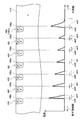
図14の上図は、従来の半導体装置の外周耐圧領域の断面図を示しており、図14の下図は、外周耐圧領域内における電界分布を示している。図14の下図では、半導体基板の表面近傍における電界を示している。各ガードリング100内では、p型不純物濃度が、中央部で高く、周辺部(外周ドリフト領域110に近い部分)に近づくにしたがって低くなるように分布している。図14では、p型不純物濃度が高い高濃度領域をp+領域として示し、p型不純物濃度が低い低濃度領域をp−領域として示している。外周耐圧領域に空乏層が広がると、各ガードリング100の外周側の端部に位置するpn接合100a(ガードリング100と外周ドリフト領域110の界面)に電界が発生する。最も外周側のガードリングである最外周ガードリング100xにおける電界の分布範囲の幅Wa1は、その他のガードリング100における電界の分布範囲の幅Wb1よりも広い。このように幅Wa1が幅Wb1より広くなる理由は、最外周ガードリング100xはその外周側にガードリング100を有さないのに対し、他のガードリング100はその外周側に隣接するガードリング100を有するためである。幅Wa1が幅Wb1よりも広いので、最外周ガードリング100xの内部で電界が発生する部分の幅Wa2が、他のガードリング100の内部で電界が発生する部分の幅Wb2よりも広い。このため、最外周ガードリング100xでは、高濃度領域(p+領域)に電界が印加される。高濃度領域内には結晶欠陥が高密度で存在しているため、高濃度領域に電界が印加されると、リーク電流が生じる。このように、従来の半導体装置では、最外周ガードリングにおいてリーク電流が生じやすいという問題があった。
The upper diagram of FIG. 14 shows a cross-sectional view of the peripheral breakdown voltage region of the conventional semiconductor device, and the lower diagram of FIG. 14 shows the electric field distribution in the peripheral breakdown voltage region. The lower diagram in FIG. 14 shows an electric field in the vicinity of the surface of the semiconductor substrate. In each
本明細書が開示する半導体装置は、半導体基板と、前記半導体基板の表面に接している表面電極と、前記半導体基板の裏面に接している裏面電極を有している。前記半導体基板が、前記半導体基板の厚み方向に沿って平面視したときに前記表面電極と前記半導体基板との接触面と重複する素子領域と、前記素子領域の周囲の外周耐圧領域を有している。前記素子領域が、前記表面電極と前記裏面電極の間に通電することが可能な半導体素子を有している。前記外周耐圧領域が、前記表面に臨んでおり、前記素子領域を多重に囲むp型の複数のガードリングと、前記複数のガードリングを互いから分離しているn型の外周ドリフト領域を有している。前記ガードリングのそれぞれが、自身のp型不純物濃度のピーク値の10%よりも高いp型不純物濃度を有する高濃度領域と、そのピーク値の10%以下のp型不純物濃度を有するとともに前記高濃度領域と前記外周ドリフト領域の間に配置されている低濃度領域を有している。前記複数のガードリングのうちの最も外周側に位置する最外周ガードリングの前記低濃度領域が、前記最外周ガードリングの前記高濃度領域の外周側に位置する第1部分を有する。前記各ガードリングの前記低濃度領域が、前記複数の高濃度領域のうちの隣接する2つに挟まれた範囲内に位置する第2部分を有する。前記第1部分の前記表面における幅が、前記第2部分の前記表面における幅のいずれよりも広い。 A semiconductor device disclosed in this specification includes a semiconductor substrate, a surface electrode in contact with the surface of the semiconductor substrate, and a back electrode in contact with the back surface of the semiconductor substrate. The semiconductor substrate has an element region overlapping with a contact surface between the surface electrode and the semiconductor substrate when viewed in plan along the thickness direction of the semiconductor substrate, and an outer peripheral breakdown voltage region around the element region. Yes. The element region includes a semiconductor element that can be energized between the front electrode and the back electrode. The outer peripheral withstand voltage region faces the surface, and has a plurality of p-type guard rings that multiplexly surround the element region, and an n-type outer peripheral drift region that separates the plurality of guard rings from each other. ing. Each of the guard rings has a high concentration region having a p-type impurity concentration higher than 10% of the peak value of its own p-type impurity concentration, a p-type impurity concentration of 10% or less of the peak value, and the high value. A low concentration region is disposed between the concentration region and the peripheral drift region. The low concentration region of the outermost peripheral guard ring located on the outermost peripheral side of the plurality of guard rings has a first portion located on the outer peripheral side of the high concentration region of the outermost peripheral guard ring. The low concentration region of each guard ring has a second portion located within a range sandwiched between two adjacent ones of the plurality of high concentration regions. The width of the first portion on the surface is wider than any of the widths of the second portion on the surface.
なお、本明細書において、第1部分及び第2部分の幅は、内周側(素子領域側)から外周側(半導体基板の外周端面側)に向かう方向における寸法を意味する。 In the present specification, the widths of the first portion and the second portion mean dimensions in a direction from the inner peripheral side (element region side) to the outer peripheral side (the outer peripheral end surface side of the semiconductor substrate).
図15は、本明細書が開示する半導体装置の一例を示している。図15の上図は、外周耐圧領域の断面図を示しており、図15の下図は、外周耐圧領域内における電界分布を示している。図15では、複数のガードリング200と外周ドリフト領域210が示されている。各ガードリング200が、p型不純物濃度が高い高濃度領域(p+領域)とp型不純物濃度が低い低濃度領域(p−領域)を有している。なお、高濃度領域内の結晶欠陥密度は、低濃度領域内の結晶欠陥密度よりも高い。各ガードリング200において、低濃度領域は、高濃度領域と外周ドリフト領域210の間に配置されている。最外周ガードリング200xの低濃度領域は、最外周ガードリング200xの高濃度領域の外周側に位置する第1部分201を有する。また、各低濃度領域は、隣接する一対の高濃度領域に挟まれた範囲内に、第2部分202を有する。第1部分201の表面における幅Wc1は、第2部分202の表面における幅Wd1のいずれよりも広い。外周耐圧領域に空乏層が広がると、各ガードリング200の外周側の端部に位置するpn接合200aに電界が発生する。最外周ガードリング200xのpn接合200aでは電界の分布範囲の幅We1が広い。このため、第1部分201内における電界の分布範囲の幅We2も広い。しかしながら、低濃度領域である第1部分201の幅Wc1が広いので、最外周ガードリング200xの高濃度領域には電界はほとんど印加されない。結晶欠陥密度が高い高濃度領域に電界が印加され難いので、リーク電流が抑制される。また、他のガードリング200のpn接合200aでは、電界の分布範囲の幅Wf1が狭い。このため、pn接合200aに隣接する第2部分202内における電界の分布範囲の幅Wf2も狭い。このため、他のガードリング200では、pn接合200aに隣接する第2部分202の幅Wd1が狭くても、高濃度領域に電界が印加され難い。また、各高濃度領域の間の間隔が広くなると、pn接合200aに印加される電界が高くなり、半導体装置の耐圧が低下する。各第2部分202の幅Wd1を狭くすることで、高濃度領域の間の間隔を狭くすることができ、半導体装置の耐圧を確保することができる。以上に説明したように、この半導体装置によれば、ガードリング200におけるリーク電流を抑制することができるとともに、半導体装置の高い耐圧を実現することができる。なお、上記の説明では図15を用いたが、本明細書が提案する半導体装置は図15の構成に限られない。各半導体領域の位置、形状、数等を適宜変更することができる。各半導体領域の位置、形状、数等を変更したとしても、本明細書が提案する構造を有することで、ガードリングにおけるリーク電流を抑制することができるとともに、半導体装置の高い耐圧を実現することができる。
FIG. 15 illustrates an example of a semiconductor device disclosed in this specification. The upper diagram in FIG. 15 shows a cross-sectional view of the outer peripheral withstand voltage region, and the lower diagram in FIG. 15 shows the electric field distribution in the outer peripheral withstand voltage region. In FIG. 15, a plurality of
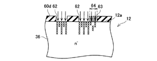
図1、2に示す実施形態の半導体装置10は、半導体基板12を有している。半導体基板12は、SiC基板である。図1に示すように、半導体基板12の表面12aには、表面電極14と絶縁膜18が設けられている。なお、図2においては、表面12a上の電極及び絶縁膜(表面電極14と絶縁膜18を含む)の図示が省略されている。図2の点線は、表面電極14と半導体基板12とが接触している接触面15の輪郭を示している。表面電極14は、半導体基板12の表面12aの中央部で半導体基板12に接している。絶縁膜18は、表面12aの表面電極14に覆われていない領域を覆っている。すなわち、絶縁膜18は、半導体基板12の表面12aの外周部を覆っている。図1に示すように、半導体基板12の裏面12bには、裏面電極16が形成されている。裏面電極16は、半導体基板12の裏面12bの全域を覆っている。以下では、半導体基板12の厚み方向に沿って見たときに接触面15と重複する領域を、素子領域20という。また、素子領域20の外側の領域(素子領域20と半導体基板12の外周端面12cの間の領域)を、外周耐圧領域22という。外周耐圧領域22は、素子領域20を囲んでいる。また、以下では、外周耐圧領域22内において、素子領域20に近い側を内周側といい、外周端面12cに近い側を外周側という。
The
図1に示すように、半導体基板12は、ドレイン領域38とドリフト領域36を有している。ドレイン領域38は、n型不純物濃度が高いn型領域である。ドレイン領域38は、素子領域20から外周耐圧領域22に跨って、半導体基板12の横方向の全域に分布している。ドレイン領域38は、半導体基板12の裏面12bに臨む範囲に配置されている。ドレイン領域38は、裏面12b全域で裏面電極16にオーミック接触している。ドリフト領域36は、ドレイン領域38よりもn型不純物濃度が低いn型領域である。ドリフト領域36は、素子領域20から外周耐圧領域22に跨って、半導体基板12の横方向の全域に分布している。ドリフト領域36は、ドレイン領域38上に配置されており、ドレイン領域38に接している。
As shown in FIG. 1, the
素子領域20内には、複数のゲート電極30、複数のソース領域32及びボディ領域34が設けられている。素子領域20内の半導体基板12の表面12aに複数のトレンチが設けられている。各トレンチ内に、ゲート電極30が配置されている。各ゲート電極30は、トレンチの内面を覆うゲート絶縁膜によって半導体基板12から絶縁されている。各ゲート電極30の上面は層間絶縁膜によって覆われており、その層間絶縁膜の上面は表面電極14に覆われている。各ゲート電極30は、層間絶縁膜によって表面電極14から絶縁されている。
In the
各ソース領域32は、n型不純物濃度が高いn型領域である。各ソース領域32は、半導体基板12の表面12aに臨む範囲に配置されている。各ソース領域32は、表面電極14にオーミック接触している。各ソース領域32は、トレンチの上端部においてゲート絶縁膜に接している。
Each
ボディ領域34は、p型領域である。ボディ領域34は、各ソース領域32に隣接する位置(表面12aに臨む位置)から各ソース領域32の下側の位置まで伸びている。ボディ領域34内のp型不純物濃度は、表面12aに臨む位置で高く、ソース領域32の下側の位置で低い。ボディ領域34は、表面12aに臨む位置で、表面電極14にオーミック接触している。ボディ領域34は、各ソース領域32の下側の位置で、ゲート絶縁膜に接している。ボディ領域34の下側に、ドリフト領域36が配置されている。ボディ領域34はドリフト領域36に接している。ドリフト領域36は、ボディ領域34の下側でゲート絶縁膜に接している。
素子領域20内には、ゲート電極30、ソース領域32、ボディ領域34、ドリフト領域36及びドレイン領域38によって、MOSFETが形成されている。MOSFETがオンすると、裏面電極16から表面電極14へ電流が流れる。
In the
外周耐圧領域22には、複数のガードリング40が設けられている。各ガードリング40は、p型領域である。図1〜3に示すように、各ガードリング40は、外周耐圧領域22内で半導体基板12の表面12aに臨んでいる(すなわち、表面12aに露出している)。図2に示すように、各ガードリング40は、半導体基板12を厚み方向に平面視したときに、環状に伸びている。複数のガードリング40は、素子領域20を多重に囲んでいる。図3に示すように、各ガードリング40の間の位置に、ドリフト領域36の一部が配置されている。ドリフト領域36によって、各ガードリング40が互いから分離されている。また、ドリフト領域36によって、最も内周側のガードリング40がボディ領域34から分離されている。各ガードリング40の上面は、絶縁膜18によって覆われている。
A plurality of guard rings 40 are provided in the outer peripheral pressure
各ガードリング40の内部において、p型不純物濃度が位置によって変化している。図3に示すように、各ガードリング40は、半導体基板12の表面12aの近傍の位置に、p型不純物濃度が自身の中で最も高いピークポイントMを有している。各ガードリング40の内部において、ピークポイントMからドリフト領域36に近づくにしたがってp型不純物濃度が低下する。本明細書では、各ガードリング40において、ピークポイントMにおけるp型不純物濃度の10%よりも高いp型不純物濃度を有する領域を高濃度領域42といい、ピークポイントMにおけるp型不純物濃度の10%以下のp型不純物濃度を有する領域を低濃度領域44という。図3において、高濃度領域42はp+型の領域として示されており、低濃度領域44はp−型の領域として示されている。各ガードリング40において、高濃度領域42はピークポイントMの周囲に分布しており、半導体基板12の表面12aに臨んでいる。各ガードリング40において、低濃度領域44は、高濃度領域42とドリフト領域36の間に分布している。すなわち、各ガードリング40において、低濃度領域44は、高濃度領域42の側方と、高濃度領域42の下側に配置されている。高濃度領域42は、半導体基板12に高濃度にp型不純物を注入することによって形成されるので、高濃度領域42内には高密度に結晶欠陥が存在している。低濃度領域44は、高濃度領域42から拡散したp型不純物や半導体基板12に低濃度に注入されたp型不純物によって形成されるので、低濃度領域44内の結晶欠陥の密度は低い。
Inside each
各ガードリング40において、低濃度領域44は、高濃度領域42の内周側と外周側の両方で表面12aに臨んでいる。以下では、各ガードリング40において、高濃度領域42に対して外周側で隣接する部分の低濃度領域44を外周側部分51といい、高濃度領域42に対して内周側で隣接する部分の低濃度領域44を内周側部分52という。図3から明らかなように、最も外周側に位置するガードリング40xの外周側部分51xと最も内周側に位置するガードリング40の内周側部分52zとを除いて、外周側部分51と内周側部分52は、いずれか2つの高濃度領域42(隣接する一対の高濃度領域42)によって挟まれた範囲に配置されている。
In each
複数のガードリング40の中で最も外周側に位置する最外周ガードリング40xの低濃度領域44は、幅が広い外周側部分51xを有している。表面12aにおいて、最外周ガードリング40xの外周側部分51xの幅W51xは、その他の外周側部分51の幅W51及び内周側部分52の幅W52よりも広い。なお、幅W51x、W51及びW52は、内周側から外周側に向かう方向における寸法である。幅W51と幅W52は、略等しい。各高濃度領域42の幅は、略等しい。このため、最外周ガードリング40xの幅は、他のガードリング40の幅よりも広い。
The low-
図1〜3に示すように、外周耐圧領域22には、端部n型領域48が設けられている。端部n型領域48は、ドリフト領域36よりもn型不純物濃度が高いn型領域である。端部n型領域48は、表面12a及び外周端面12cに臨む範囲に配置されている。端部n型領域48は、外周端面12cに沿って環状に伸びている。端部n型領域48は、ドリフト領域36によって最外周ガードリング40xから分離されている。端部n型領域48と最外周ガードリング40xの間の間隔は、各ガードリング40の間の間隔よりも広い。
As shown in FIGS. 1 to 3, an end n-
次に、半導体装置10の動作について説明する。半導体装置10の動作時には、裏面電極16に対して表面電極14よりも高い電位が印加される。ゲート電極30に閾値よりも高い電位が印加されると、ゲート絶縁膜に接する範囲のボディ領域34にチャネルが形成される。すると、表面電極14から、ソース領域32、チャネル、ドリフト領域36及びドレイン領域38を介して裏面電極16へ電子が流れる。すなわち、MOSFETがオンする。ゲート電極30の電位を閾値以下に低下させると、チャネルが消失し、電子の流れが停止する。すなわち、MOSFETがオフする。MOSFETがオフする際に、ボディ領域34からドリフト領域36内に空乏層が広がる。素子領域20内のドリフト領域36内では、表面側から裏面側に空乏層が広がる。外周耐圧領域22内のドリフト領域36内では、内周側から外周側に向かって空乏層が広がる。ボディ領域34から伸びる空乏層が最も内周側のガードリング40に到達すると、そのガードリング40からさらに外周側に空乏層が伸びる。最も内周側のガードリング40から伸びる空乏層が内周側から2番目のガードリング40に到達すると、そのガードリング40からさらに外周側に空乏層が伸びる。このように、外周耐圧領域22においては、空乏層が複数のガードリング40を経由しながら外周側に伸びる。すなわち、各ガードリング40は、空乏層が外周側に伸びるのを促進する。空乏層は、端部n型領域48の近傍まで伸びる。
Next, the operation of the
外周耐圧領域22内のドリフト領域36に空乏層が伸びると、各ガードリング40の外周側の端部に位置するpn接合40aに電圧が印加される。このため、各pn接合40aの近傍で、低濃度領域44が空乏化される。すなわち、pn接合40aから外周側部分51内に空乏層が広がる。各pn接合40aの両側の空乏層(すなわち、n型のドリフト領域36が空乏化した空乏層とp型の低濃度領域44の外周側部分51が空乏化した空乏層)の内部に、電界が生じる。ここで、最外周ガードリング40xのpn接合40aで電界が生じる部分の幅Wx1は、その他のガードリング40のpn接合40aで電界が生じる部分の幅Wy1よりも広い。このため、最外周ガードリング40xの外周側部分51x内で電界が生じる部分(空乏化する部分)の幅Wx2は、他のガードリング40の外周側部分51内で電界が生じる部分の幅Wy2よりも広い。他方、上述したように、最外周ガードリング40xの外周側部分51xの幅W51xは、他のガードリング40の外周側部分51の幅W51よりも広い。このため、最外周ガードリング40xでは、電界が生じる部分の幅Wx2が広くても、その電界が生じる部分が高濃度領域42まで達しない(すなわち、W51x>Wx2の関係が成立している。)。このように、最外周ガードリング40xでは、高濃度領域42の外周側に幅が広い外周側部分51xが設けられているので、高濃度領域42に電界が加わることが抑制される。すなわち、広い幅W51xを有する外周側部分51xを空乏化させることで、高濃度領域42まで空乏層が達することを抑制することができる。結晶欠陥密度が高い高濃度領域42にほとんど電界が加わらないので、高濃度領域42でリーク電流がほとんど生じない。また、結晶欠陥密度が低い外周側部分51x(すなわち、低濃度領域44)に電界が印加されても、リーク電流はほとんど生じない。したがって、最外周ガードリング40xにおけるリーク電流を抑制することができる。
When the depletion layer extends into the
また、最外周ガードリング40x以外のガードリング40では、外周側部分51の幅W51が狭い。しかしながら、これらのガードリングでは、電界が生じる部分の幅Wy2が狭い。したがって、外周側部分51の幅W51が狭くても、高濃度領域42に電界が加わり難い。したがって、最外周ガードリング40x以外のガードリング40でもリーク電流が抑制される。
Further, in the guard rings 40 other than the outermost
また、高濃度領域42の間の間隔が広くなると、pn接合40aに電界が集中し易くなり、半導体装置10の耐圧が低下する。これに対し、本実施形態では、最外周ガードリング40xの外周側部分51xの幅W51xが広い一方で、その他の外周側部分51の幅W51、及び、内周側部分52の幅W52が狭い。このため、高濃度領域42の間の間隔が狭い。これによって、半導体装置10の耐圧が確保されている。また、高濃度領域42の間の間隔を狭くすることで、半導体装置10の小型化が図られている。
Further, when the interval between the
次に、半導体装置10の製造方法について説明する。なお、この製造方法は、ガードリング40の形成工程に特徴を有するので、以下ではガードリング40の形成工程について説明し、他の工程については説明を省略する。また、以下の説明で用いる図4〜13は、最外周ガードリング40xと、その隣のガードリング40を形成すべき範囲を示している。
Next, a method for manufacturing the
図4〜6は、第1の製造方法を示している。最初に、n型のドリフト領域36が表面12aに露出している半導体基板12(加工前の半導体基板)を準備する。次に、図4に示すように、半導体基板12の表面12aにイオン注入用のマスク60a(酸化膜またはレジスト等)を形成する。マスク60aは、各ガードリング40に対応する位置に開口部62が設けられるようにパターニングして形成する。次に、不純物の注入エネルギー(すなわち、不純物の注入深さ)を変更しながら、マスク60aを介して半導体基板12に複数回、p型不純物を注入する。これによって、開口部62の下側の半導体層にp型不純物を注入する。ここでは、浅い範囲に高濃度にp型不純物を注入し、深い範囲に低濃度にp型不純物を注入する。高濃度にp型不純物が注入された範囲(浅い範囲)には、高濃度に結晶欠陥が生成される。次に、図5に示すように、最も外周側の開口部62(すなわち、最外周ガードリング40xに対応する開口部62)の幅を拡大する。より詳細には、最も外周側の開口部62の外周側の壁面をさらに外周側にシフトさせることで、この開口部62の幅を拡大する。マスク60aが酸化膜の場合には、マスク60aを選択的に追加エッチングすることで、図5のように開口部62の幅を広げることができる。マスク60aがレジストの場合には、図4に示すマスク60aを除去した後、図5に示す新たなパターンのマスク60aを形成することで開口部62の幅を広げることができる。次に、開口部62を拡大したマスク60aを介して、半導体基板12にp型不純物を注入する。ここでは、浅い範囲と深い範囲の両方に低濃度にp型不純物を注入する。このため、開口部62の拡大された範囲では、半導体基板12の浅い範囲と深い範囲に低濃度にp型不純物が分布する。その後、マスク60aを除去し、注入したp型不純物を活性化させるアニールを行うことで、図6に示すようにガードリング40が形成される。半導体基板12をアニールする際にガードリング40内に存在する結晶欠陥の一部が消滅するが、アニール後に所定の割合で結晶欠陥が残存する。p型不純物が高濃度に注入された高濃度領域42内では、p型不純物が低濃度に注入された低濃度領域44内よりも、結晶欠陥密度が高くなる。また、この製造方法によれば、開口部62を拡大した範囲に幅が広い外周側部分51xが形成される。この製造方法によれば、外周側部分51xの幅が広い最外周ガードリング40xを形成することができる。
4 to 6 show the first manufacturing method. First, the semiconductor substrate 12 (semiconductor substrate before processing) in which the n-
図7、8は、第2の製造方法を示している。第2の製造方法では、図7に示すように、半導体基板12の表面12aに開口部62を有するマスク60bを形成する。ここでは、最も外周側の開口部62(すなわち、最外周ガードリング40xに対応する開口部62)の外周側の壁面が傾斜するようにマスク60bを形成する。次に、不純物の注入エネルギーを変更しながら、マスク60bを介して半導体基板12に複数回、p型不純物を注入する。これによって、開口部62の下側の半導体層にp型不純物を注入する。ここでは、浅い範囲に高濃度にp型不純物を注入し、深い範囲に低濃度にp型不純物を注入する。ここで、開口部62の傾斜する壁面の部分61aでは、マスク60bの厚みが薄い。したがって、深い範囲へのイオン注入時に、p型不純物が、部分61aを貫通して半導体基板12に注入される。したがって、部分61aの下側の半導体層に低濃度にp型不純物が注入される。部分61aの下側の半導体層には、浅い範囲に低濃度にp型不純物が注入される。その後、マスク60bを除去し、注入したp型不純物を活性化させるアニールを行うことで、図8に示すようにガードリング40が形成される。この製造方法によれば、外周側部分51xの幅が広い最外周ガードリング40xを形成することができる。
7 and 8 show the second manufacturing method. In the second manufacturing method, as shown in FIG. 7, a
なお、第2の製造方法において、マスク60bの代わりに、図9に示すマスク60cを用いてもよい。図9に示すマスク60cは、図7の傾斜した壁面を有する部分61aの代わりに、厚みが薄い部分61bを有している。マスク60bを用いる場合には、イオン注入時に、部分61bの下側の半導体層に低濃度にp型不純物が注入される。マスク60cを用いても、外周側部分51xの幅が広い最外周ガードリング40xを形成することができる。
In the second manufacturing method, a
図10、11は、第3の製造方法を示している。第3の製造方法では、図10、11に示すように、半導体基板12の表面12aに開口部62を有するマスク60dを形成する。マスク60dは、最も外周側の開口部62(すなわち、最外周ガードリング40xに対応する開口部62)のさらに外周側に、多数の微小な開口部63が設けられた領域64を有する。微小な開口部63の密度は、開口部62に近い位置では高く、開口部62から遠い位置では低い。つまり、領域64における開口率が、開口部62から遠い位置ほど低くなっている。次に、不純物の注入エネルギーを変更しながら、マスク60dを介して半導体基板12に複数回、p型不純物を注入する。ここでは、浅い範囲に高濃度にp型不純物を注入し、深い範囲に低濃度にp型不純物を注入する。マスク60dの領域64では、微小な開口部63を介して半導体基板12にp型不純物が注入される。領域64の開口率が低いので、領域64の下側の半導体層に低濃度にp型不純物が注入される。特に、領域64では開口部62から遠い位置ほど開口率が低くなっているので、領域64の下側の半導体層には開口部62から遠い位置ほど低濃度にp型不純物が注入される。その後、マスク60dを除去し、注入したp型不純物を活性化させるアニールを行うことで、図8と同様にガードリング40が形成される。この製造方法によれば、外周側部分51xの幅が広い最外周ガードリング40xを形成することができる。
10 and 11 show a third manufacturing method. In the third manufacturing method, as shown in FIGS. 10 and 11, a
なお、第3の製造方法において、マスク60dの代わりに、図12に示すマスク60eを用いてもよい。マスク60eでは、領域64において、微小な開口部63のサイズが、開口部62に近い位置では大きく、開口部62から遠い位置では小さい。つまり、領域64における開口率が、開口部62から遠い位置ほど低くなっている。したがって、図12に示すマスク60eを用いても、外周側部分51xの幅が広い最外周ガードリング40xを形成することができる。
In the third manufacturing method, a
図4、13は、第4の製造方法を示している。第4の製造方法では、まず、図4に示すように、開口部62を有するマスク60aを形成し、マスク60aを介して半導体基板12にp型不純物を注入する。マスク60aの形成工程、及び、マスク60aを介したp型不純物の注入工程は、第1の製造方法と同様である。次に、図13に示すように、最も外周側の開口部62の外周側の壁面近傍が露出し、その他の部分が覆われるように、マスク60a上にレジスト65を形成する。そして、半導体基板12の表面12aに対して内周側から外周側に向かう方向にイオン注入角度を傾斜させて、半導体基板12にp型不純物を注入する。p型不純物は、レジスト65に覆われていない範囲のマスク60aを部分的に貫通して、その下側の半導体層に注入される。すなわち、レジスト65に覆われていない範囲のマスク60aの下部の半導体層に、低濃度にp型不純物が注入される。なお、図2に示すように、最外周ガードリング40xは素子領域20を囲むように環状に形成されるので、最外周ガードリング40xの各部分に対して内周側から外周側に向かって傾斜した角度でp型不純物を注入できるように、注入方向を傾斜させる向きを変更しながら複数回注入を行う。その後、マスク60a、レジスト65を除去し、注入したp型不純物を活性化させるアニールを行うことで、図8と同様にガードリング40が形成される。この製造方法によれば、外周側部分51xの幅が広い最外周ガードリング40xを形成することができる。
4 and 13 show a fourth manufacturing method. In the fourth manufacturing method, first, as shown in FIG. 4, a
なお、上述した実施形態では、素子領域20にMOSFETが形成されていたが、素子領域20に他の半導体素子が設けられていてもよい。例えば、素子領域20にIGBTが設けられていてもよい。ドレイン領域38に代えてp型のコレクタ領域を設けることで、IGBTを得ることができる。また、例えば、表面電極14がアノード電極として機能し、裏面電極16がカソード電極として機能するダイオード(pnダイオード、ショットキーバリアダイオード等)が素子領域に設けられていてもよい。ダイオードが形成されている場合には、アノード‐カソード間に逆電圧が印加されると、外周耐圧領域に空乏層が広がり、上述した実施形態と同様の効果を得ることができる。
In the above-described embodiment, the MOSFET is formed in the
また、上述した実施形態では、高濃度領域42のp型不純物濃度が、ピークポイントMにおけるp型不純物濃度の10%よりも高いp型不純物濃度を有していた。高濃度領域42の空乏化をより確実に防ぐために、高濃度領域42が1×10¹⁸atoms/cm3より高いp型不純物濃度を有していることが好ましい。
In the above-described embodiment, the p-type impurity concentration in the
また、上述した実施形態では、半導体基板12がSiCにより構成されていたが、他の半導体材料(例えば、SiC以外の化合物半導体材料またはシリコン等)により半導体基板12が構成されていてもよい。但し、SiC基板では、p型不純物の拡散範囲を制御し易く、ガードリングを正確に形成し易い。したがって、SiC基板は、本願明細書が開示する技術により適している。
In the above-described embodiment, the
上述した実施形態の各構成要素と請求項の各構成要素との関係について説明する。実施形態のMOSFETは、請求項の半導体素子の一例である。実施形態の外周耐圧領域22内のドリフト領域36は、請求項の外周ドリフト領域の一例である。実施形態の外周側部分51xは、請求項の第1部分の一例である。実施形態の外周側部分51x以外の外周側部分51と内周側部分52z以外の内周側部分52は、請求項の第2部分の一例である。上記第2、第3及び第4の製造方法において、最外周ガードリング40xの外周側部分51xの上部のマスク(低濃度のp型不純物が通過する部分のマスク)は、請求項の低透過率部の一例である。上記第2、第3及び第4の製造方法において、開口部62は、請求項の開口部の一例である。上記第2、第3及び第4の製造方法において、p型不純物を遮蔽する部分のマスク(ガードリング40を形成しない領域の上部のマスク)は、請求項の遮蔽部の一例である。
The relationship between each component of the embodiment described above and each component of the claims will be described. The MOSFET according to the embodiment is an example of a semiconductor element in claims. The
本明細書が開示する技術要素について、以下に列記する。なお、以下の各技術要素は、それぞれ独立して有用なものである。 The technical elements disclosed in this specification are listed below. The following technical elements are each independently useful.
本明細書の一例に係る半導体装置の製造方法は、半導体基板にp型不純物を注入することによって、半導体基板の表面に臨んでおり、特定領域を多重に囲むp型の複数のガードリングを形成する工程と、半導体基板を用いて半導体装置を完成させる工程を有する。 A method of manufacturing a semiconductor device according to an example of the present specification forms a plurality of p-type guard rings that face a surface of a semiconductor substrate by injecting p-type impurities into the semiconductor substrate and surround a specific region in multiple layers. And a step of completing a semiconductor device using a semiconductor substrate.
なお、半導体装置を完成させる工程の一部を、ガードリングを形成する工程の前で行ってもよい。 Note that a part of the process of completing the semiconductor device may be performed before the process of forming the guard ring.
本明細書の一例に係る半導体装置の製造方法では、ガードリングを形成する工程が、半導体基板の表面に開口部と遮蔽部と低透過率部を有するマスクを形成する工程と、マスクを介して半導体基板にp型不純物を注入する工程を有する。p型不純物を注入する工程において、低透過率部におけるp型不純物の透過率が、開口部におけるp型不純物の透過率よりも低いとともに、遮蔽部におけるp型不純物の透過率よりも高い。開口部の下側に位置する半導体基板内の領域に高濃度領域が形成される。低透過率部の下側に位置する半導体基板内の領域に第1部分が形成される。 In the method for manufacturing a semiconductor device according to an example of the present specification, the step of forming the guard ring includes a step of forming a mask having an opening, a shielding portion, and a low-transmittance portion on the surface of the semiconductor substrate. A step of implanting p-type impurities into the semiconductor substrate; In the step of injecting the p-type impurity, the transmittance of the p-type impurity in the low transmittance portion is lower than the transmittance of the p-type impurity in the opening and higher than the transmittance of the p-type impurity in the shielding portion. A high concentration region is formed in a region in the semiconductor substrate located below the opening. A first portion is formed in a region in the semiconductor substrate located below the low transmittance portion.
この製造方法によれば、最外周ガードリングの低濃度領域の第1部分を好適に形成することができる。 According to this manufacturing method, the first portion of the low concentration region of the outermost guard ring can be suitably formed.
以上、実施形態について詳細に説明したが、これらは例示にすぎず、特許請求の範囲を限定するものではない。特許請求の範囲に記載の技術には、以上に例示した具体例をさまざまに変形、変更したものが含まれる。本明細書または図面に説明した技術要素は、単独あるいは各種の組み合わせによって技術有用性を発揮するものであり、出願時請求項記載の組み合わせに限定されるものではない。また、本明細書または図面に例示した技術は複数目的を同時に達成するものであり、そのうちの1つの目的を達成すること自体で技術有用性を持つものである。 The embodiments have been described in detail above, but these are merely examples and do not limit the scope of the claims. The technology described in the claims includes various modifications and changes of the specific examples illustrated above. The technical elements described in this specification or the drawings exhibit technical usefulness alone or in various combinations, and are not limited to the combinations described in the claims at the time of filing. In addition, the technology exemplified in this specification or the drawings achieves a plurality of objects at the same time, and has technical usefulness by achieving one of them.
10 :半導体装置
12 :半導体基板
14 :表面電極
15 :コンタクト面
16 :裏面電極
18 :絶縁膜
20 :素子領域
22 :外周耐圧領域
30 :カソード領域
32 :ドリフト領域
32a:メインドリフト領域
32b:外周ドリフト領域
34 :メインp型領域
34a:環状領域
34b:ストライプ領域
36 :ガードリング
40 :高濃度領域
42 :低濃度領域
DESCRIPTION OF SYMBOLS 10: Semiconductor device 12: Semiconductor substrate 14: Front surface electrode 15: Contact surface 16: Back surface electrode 18: Insulating film 20: Element region 22: Outer peripheral pressure | voltage resistant region 30: Cathode region 32: Drift region 32a: Main drift region 32b: Outer periphery drift Region 34: Main p-type region 34a: Ring region 34b: Stripe region 36: Guard ring 40: High concentration region 42: Low concentration region
Claims (4)
半導体基板と、
前記半導体基板の表面に接している表面電極と、
前記半導体基板の裏面に接している裏面電極、
を有しており、
前記半導体基板が、前記半導体基板の厚み方向に沿って平面視したときに前記表面電極と前記半導体基板との接触面と重複する素子領域と、前記素子領域の周囲の外周耐圧領域を有しており、
前記素子領域が、前記表面電極と前記裏面電極の間に通電することが可能な半導体素子を有しており、
前記外周耐圧領域が、
前記表面に臨んでおり、前記素子領域を多重に囲むp型の複数のガードリングと、
前記複数のガードリングを互いから分離しているn型の外周ドリフト領域、
を有しており、
前記ガードリングのそれぞれが、自身のp型不純物濃度のピーク値の10%よりも高いp型不純物濃度を有する高濃度領域と、そのピーク値の10%以下のp型不純物濃度を有するとともに前記高濃度領域と前記外周ドリフト領域の間に配置されている低濃度領域を有しており、
前記複数のガードリングのうちの最も外周側に位置する最外周ガードリングの前記低濃度領域が、前記最外周ガードリングの前記高濃度領域の外周側に位置する第1部分を有し、
前記ガードリングのそれぞれの前記低濃度領域が、前記複数の高濃度領域のうちの隣接する2つに挟まれた範囲内に位置する第2部分を有し、
前記第1部分の前記表面における幅が、前記第2部分の前記表面における幅のいずれよりも広い、
半導体装置。 A semiconductor device,
A semiconductor substrate;
A surface electrode in contact with the surface of the semiconductor substrate;
A back electrode in contact with the back surface of the semiconductor substrate;
Have
The semiconductor substrate has an element region overlapping with a contact surface between the surface electrode and the semiconductor substrate when viewed in plan along the thickness direction of the semiconductor substrate, and an outer peripheral breakdown voltage region around the element region. And
The element region has a semiconductor element that can be energized between the front electrode and the back electrode,
The outer peripheral pressure resistance region is
A plurality of p-type guard rings facing the surface and surrounding the element region in multiple layers;
An n-type peripheral drift region separating the plurality of guard rings from each other;
Have
Each of the guard rings has a high concentration region having a p-type impurity concentration higher than 10% of the peak value of its own p-type impurity concentration, a p-type impurity concentration of 10% or less of the peak value, and the high value. Having a low concentration region disposed between the concentration region and the peripheral drift region;
The low-concentration region of the outermost peripheral guard ring located on the outermost peripheral side of the plurality of guard rings has a first portion located on the outer peripheral side of the high-concentration region of the outermost peripheral guard ring;
Each of the low concentration regions of the guard ring has a second portion located within a range sandwiched between two adjacent ones of the plurality of high concentration regions;
The width of the first portion on the surface is wider than any of the widths of the second portion on the surface;
Semiconductor device.
半導体基板にp型不純物を注入することによって、前記半導体基板の表面に臨んでおり、特定領域を多重に囲むp型の複数のガードリングを形成する工程と、
前記半導体基板を用いて半導体装置を完成させる工程、
を有し、
前記半導体装置が、前記特定領域内の前記表面に接している表面電極と、
前記半導体基板の裏面に接している裏面電極と、
前記特定領域内に設けられており、前記表面電極と前記裏面電極の間に通電することが可能な半導体素子と、
前記複数のガードリングを互いから分離しているn型の外周ドリフト領域、
を有しており、
前記ガードリングのそれぞれが、自身のp型不純物濃度のピーク値の10%よりも高いp型不純物濃度を有する高濃度領域と、そのピーク値の10%以下のp型不純物濃度を有するとともに前記高濃度領域と前記外周ドリフト領域の間に配置されている低濃度領域を有しており、
前記複数のガードリングのうちの最も外周側に位置する最外周ガードリングの前記低濃度領域が、前記最外周ガードリングの前記高濃度領域の外周側に位置する第1部分を有し、
前記ガードリングのそれぞれの前記低濃度領域が、前記複数の高濃度領域のうちの隣接する2つに挟まれた範囲内に位置する第2部分を有し、
前記第1部分の前記表面における幅が、前記第2部分の前記表面における幅のいずれよりも広い、
製造方法。 A method for manufacturing a semiconductor device, comprising:
Forming a plurality of p-type guard rings facing the surface of the semiconductor substrate by multiplying p-type impurities into the semiconductor substrate and surrounding the specific region in multiple layers;
A step of completing a semiconductor device using the semiconductor substrate;
Have
The semiconductor device has a surface electrode in contact with the surface in the specific region;
A back electrode in contact with the back surface of the semiconductor substrate;
A semiconductor element which is provided in the specific region and can be energized between the front electrode and the back electrode;
An n-type peripheral drift region separating the plurality of guard rings from each other;
Have
Each of the guard rings has a high concentration region having a p-type impurity concentration higher than 10% of the peak value of its own p-type impurity concentration, a p-type impurity concentration of 10% or less of the peak value, and the high value. Having a low concentration region disposed between the concentration region and the peripheral drift region;
The low-concentration region of the outermost peripheral guard ring located on the outermost peripheral side of the plurality of guard rings has a first portion located on the outer peripheral side of the high-concentration region of the outermost peripheral guard ring;
Each of the low concentration regions of the guard ring has a second portion located within a range sandwiched between two adjacent ones of the plurality of high concentration regions;
The width of the first portion on the surface is wider than any of the widths of the second portion on the surface;
Production method.
前記半導体基板の前記表面に、開口部と、遮蔽部と、低透過率部を有するマスクを形成する工程と、
前記マスクを介して前記半導体基板にp型不純物を注入する工程、
を有し、
前記p型不純物を注入する工程において、前記低透過率部におけるp型不純物の透過率が、前記開口部におけるp型不純物の透過率よりも低いとともに、前記遮蔽部におけるp型不純物の透過率よりも高く、
前記開口部の下側に位置する前記半導体基板内の領域に前記高濃度領域が形成され、
前記低透過率部の下側に位置する前記半導体基板内の領域に前記第1部分が形成される、
請求項3の製造方法。 Forming the guard ring comprises:
Forming a mask having an opening, a shielding part, and a low transmittance part on the surface of the semiconductor substrate;
Implanting p-type impurities into the semiconductor substrate through the mask;
Have
In the step of injecting the p-type impurity, the transmittance of the p-type impurity in the low-transmittance portion is lower than the transmittance of the p-type impurity in the opening, and more than the transmittance of the p-type impurity in the shielding portion. Higher
The high-concentration region is formed in a region in the semiconductor substrate located below the opening;
The first portion is formed in a region in the semiconductor substrate located below the low transmittance portion;
The manufacturing method of Claim 3.
Priority Applications (4)
| Application Number | Priority Date | Filing Date | Title |
|---|---|---|---|
| JP2016207266A JP2018067690A (en) | 2016-10-21 | 2016-10-21 | Semiconductor device and manufacturing method of the same |
| CN201780062414.9A CN109844954B (en) | 2016-10-21 | 2017-09-26 | Semiconductor device and method for manufacturing the same |
| US16/339,223 US10985241B2 (en) | 2016-10-21 | 2017-09-26 | Semiconductor device and production method thereof |
| PCT/IB2017/001168 WO2018073638A1 (en) | 2016-10-21 | 2017-09-26 | Semiconductor device and production method thereof |
Applications Claiming Priority (1)
| Application Number | Priority Date | Filing Date | Title |
|---|---|---|---|
| JP2016207266A JP2018067690A (en) | 2016-10-21 | 2016-10-21 | Semiconductor device and manufacturing method of the same |
Publications (2)
| Publication Number | Publication Date |
|---|---|
| JP2018067690A true JP2018067690A (en) | 2018-04-26 |
| JP2018067690A5 JP2018067690A5 (en) | 2019-06-13 |
Family
ID=60782249
Family Applications (1)
| Application Number | Title | Priority Date | Filing Date |
|---|---|---|---|
| JP2016207266A Pending JP2018067690A (en) | 2016-10-21 | 2016-10-21 | Semiconductor device and manufacturing method of the same |
Country Status (4)
| Country | Link |
|---|---|
| US (1) | US10985241B2 (en) |
| JP (1) | JP2018067690A (en) |
| CN (1) | CN109844954B (en) |
| WO (1) | WO2018073638A1 (en) |
Cited By (2)
| Publication number | Priority date | Publication date | Assignee | Title |
|---|---|---|---|---|
| CN111162116A (en) * | 2018-10-19 | 2020-05-15 | 株式会社电装 | Semiconductor device and method for manufacturing the same |
| JP2020119922A (en) * | 2019-01-18 | 2020-08-06 | トヨタ自動車株式会社 | Semiconductor device |
Families Citing this family (1)
| Publication number | Priority date | Publication date | Assignee | Title |
|---|---|---|---|---|
| JP7107284B2 (en) * | 2019-07-08 | 2022-07-27 | 株式会社デンソー | Semiconductor device and its manufacturing method |
Citations (3)
| Publication number | Priority date | Publication date | Assignee | Title |
|---|---|---|---|---|
| JP2001094095A (en) * | 1999-09-21 | 2001-04-06 | Denso Corp | Silicon carbide semiconductor device and fabrication method thereof |
| WO2011141981A1 (en) * | 2010-05-10 | 2011-11-17 | 株式会社日立製作所 | Semiconductor device |
| WO2014054319A1 (en) * | 2012-10-02 | 2014-04-10 | 三菱電機株式会社 | Semiconductor device and method for manufacturing same |
Family Cites Families (12)
| Publication number | Priority date | Publication date | Assignee | Title |
|---|---|---|---|---|
| EP0311816A1 (en) * | 1987-10-15 | 1989-04-19 | BBC Brown Boveri AG | Semiconductor element and its manufacturing method |
| JP2000114549A (en) | 1998-09-30 | 2000-04-21 | Meidensha Corp | Semiconductor element |
| JP2005135972A (en) * | 2003-10-28 | 2005-05-26 | Shindengen Electric Mfg Co Ltd | Manufacturing method of semiconductor device |
| JP5358963B2 (en) * | 2008-02-04 | 2013-12-04 | 富士電機株式会社 | Semiconductor device and manufacturing method thereof |
| JP2009289904A (en) * | 2008-05-28 | 2009-12-10 | Toshiba Corp | Semiconductor device |
| EP2341528A1 (en) * | 2010-01-05 | 2011-07-06 | ABB Technology AG | Power Semiconductor Device and its manufacturing method |
| TWM410990U (en) * | 2011-02-11 | 2011-09-01 | Pynmax Technology Co Ltd | High Antistatic capability schottky diode |
| US8937319B2 (en) * | 2011-03-07 | 2015-01-20 | Shindengen Electric Manufacturing Co., Ltd. | Schottky barrier diode |
| JP5812029B2 (en) * | 2012-06-13 | 2015-11-11 | 株式会社デンソー | Silicon carbide semiconductor device and manufacturing method thereof |
| US9412809B2 (en) | 2013-02-15 | 2016-08-09 | Toyota Jidosha Kabushiki Kaisha | Semiconductor device and manufacturing method thereof |
| CN204257659U (en) * | 2014-12-19 | 2015-04-08 | 扬州国宇电子有限公司 | A kind of terminal isolation structure of semiconductor transistor |
| JP2016201448A (en) | 2015-04-09 | 2016-12-01 | トヨタ自動車株式会社 | Diode and method for manufacturing diode |
-
2016
- 2016-10-21 JP JP2016207266A patent/JP2018067690A/en active Pending
-
2017
- 2017-09-26 WO PCT/IB2017/001168 patent/WO2018073638A1/en active Application Filing
- 2017-09-26 CN CN201780062414.9A patent/CN109844954B/en active Active
- 2017-09-26 US US16/339,223 patent/US10985241B2/en active Active
Patent Citations (3)
| Publication number | Priority date | Publication date | Assignee | Title |
|---|---|---|---|---|
| JP2001094095A (en) * | 1999-09-21 | 2001-04-06 | Denso Corp | Silicon carbide semiconductor device and fabrication method thereof |
| WO2011141981A1 (en) * | 2010-05-10 | 2011-11-17 | 株式会社日立製作所 | Semiconductor device |
| WO2014054319A1 (en) * | 2012-10-02 | 2014-04-10 | 三菱電機株式会社 | Semiconductor device and method for manufacturing same |
Cited By (2)
| Publication number | Priority date | Publication date | Assignee | Title |
|---|---|---|---|---|
| CN111162116A (en) * | 2018-10-19 | 2020-05-15 | 株式会社电装 | Semiconductor device and method for manufacturing the same |
| JP2020119922A (en) * | 2019-01-18 | 2020-08-06 | トヨタ自動車株式会社 | Semiconductor device |
Also Published As
| Publication number | Publication date |
|---|---|
| US20200044018A1 (en) | 2020-02-06 |
| CN109844954B (en) | 2022-05-10 |
| US10985241B2 (en) | 2021-04-20 |
| CN109844954A (en) | 2019-06-04 |
| WO2018073638A1 (en) | 2018-04-26 |
Similar Documents
| Publication | Publication Date | Title |
|---|---|---|
| US8330185B2 (en) | Semiconductor device having semiconductor substrate including diode region and IGBT region | |
| JP2008300506A (en) | Silicon carbide semiconductor device including junction barrier schottky diode | |
| US7915705B2 (en) | SiC semiconductor device having outer periphery structure | |
| JP2016201448A (en) | Diode and method for manufacturing diode | |
| JP5865016B2 (en) | Trench type Schottky junction type semiconductor device and manufacturing method thereof | |
| WO2014087499A1 (en) | Semiconductor device | |
| CN109844954B (en) | Semiconductor device and method for manufacturing the same | |
| CN107623026B (en) | Semiconductor device and method for manufacturing the same | |
| JP2010225878A (en) | Semiconductor device with schottky barrier diode, and method of manufacturing the same | |
| KR101490937B1 (en) | Schottky barrier diode and method for manufacturing the same | |
| JP2019096732A (en) | Semiconductor device | |
| US11133406B2 (en) | Semiconductor device | |
| JPH06283727A (en) | Power semiconductor element | |
| US10840386B2 (en) | Semiconductor apparatus | |
| JP2005243716A (en) | Semiconductor device | |
| KR20210013947A (en) | Schottky barrier diode | |
| JP2005229070A (en) | Schottky barrier diode and manufacturing method therefor | |
| JP2022100379A (en) | Semiconductor device and method for manufacturing the same | |
| JP6152861B2 (en) | Diode manufacturing method | |
| CN114072922B (en) | Semiconductor device and method for manufacturing the same | |
| WO2024084778A1 (en) | Semiconductor device and method for producing same | |
| CN101728430B (en) | High-pressure metal-oxide-semiconductor component and manufacturing method thereof | |
| JP7013898B2 (en) | Manufacturing method of switching element | |
| JP2024060452A (en) | Semiconductor device and its manufacturing method | |
| JP4205609B2 (en) | Schottky barrier diode and manufacturing method thereof |
Legal Events
| Date | Code | Title | Description |
|---|---|---|---|
| A521 | Request for written amendment filed |
Free format text: JAPANESE INTERMEDIATE CODE: A523 Effective date: 20190426 |
|
| A621 | Written request for application examination |
Free format text: JAPANESE INTERMEDIATE CODE: A621 Effective date: 20190426 |
|
| A977 | Report on retrieval |
Free format text: JAPANESE INTERMEDIATE CODE: A971007 Effective date: 20200117 |
|
| A131 | Notification of reasons for refusal |
Free format text: JAPANESE INTERMEDIATE CODE: A131 Effective date: 20200121 |
|
| A521 | Request for written amendment filed |
Free format text: JAPANESE INTERMEDIATE CODE: A523 Effective date: 20200319 |
|
| A131 | Notification of reasons for refusal |
Free format text: JAPANESE INTERMEDIATE CODE: A131 Effective date: 20200519 |
|
| A711 | Notification of change in applicant |
Free format text: JAPANESE INTERMEDIATE CODE: A711 Effective date: 20200611 |
|
| A521 | Request for written amendment filed |
Free format text: JAPANESE INTERMEDIATE CODE: A821 Effective date: 20200611 |
|
| A02 | Decision of refusal |
Free format text: JAPANESE INTERMEDIATE CODE: A02 Effective date: 20200915 |