EP2814036A2 - Synapsen-Array, Impulsformungsschaltung und neuromorphes System - Google Patents
Synapsen-Array, Impulsformungsschaltung und neuromorphes System Download PDFInfo
- Publication number
- EP2814036A2 EP2814036A2 EP14169845.6A EP14169845A EP2814036A2 EP 2814036 A2 EP2814036 A2 EP 2814036A2 EP 14169845 A EP14169845 A EP 14169845A EP 2814036 A2 EP2814036 A2 EP 2814036A2
- Authority
- EP
- European Patent Office
- Prior art keywords
- circuit
- synapse
- neuron
- pulse
- circuits
- Prior art date
- Legal status (The legal status is an assumption and is not a legal conclusion. Google has not performed a legal analysis and makes no representation as to the accuracy of the status listed.)
- Granted
Links
Images


Classifications
-
- G—PHYSICS
- G11—INFORMATION STORAGE
- G11C—STATIC STORES
- G11C11/00—Digital stores characterised by the use of particular electric or magnetic storage elements; Storage elements therefor
- G11C11/54—Digital stores characterised by the use of particular electric or magnetic storage elements; Storage elements therefor using elements simulating biological cells, e.g. neuron
-
- G—PHYSICS
- G06—COMPUTING OR CALCULATING; COUNTING
- G06N—COMPUTING ARRANGEMENTS BASED ON SPECIFIC COMPUTATIONAL MODELS
- G06N3/00—Computing arrangements based on biological models
- G06N3/02—Neural networks
- G06N3/04—Architecture, e.g. interconnection topology
- G06N3/049—Temporal neural networks, e.g. delay elements, oscillating neurons or pulsed inputs
-
- G—PHYSICS
- G06—COMPUTING OR CALCULATING; COUNTING
- G06N—COMPUTING ARRANGEMENTS BASED ON SPECIFIC COMPUTATIONAL MODELS
- G06N3/00—Computing arrangements based on biological models
- G06N3/02—Neural networks
- G06N3/06—Physical realisation, i.e. hardware implementation of neural networks, neurons or parts of neurons
- G06N3/063—Physical realisation, i.e. hardware implementation of neural networks, neurons or parts of neurons using electronic means
Definitions
- the following description relates to a synapse array, a pulse shaper circuit, and a neuromorphic system that includes a synapse array and/or a pulse shaper circuit.
- a physiological brain includes hundreds of billions of neurons that are interconnected with one another in a complicated nerve network. Neurons are considered to be responsible for the intellectual capability for learning and memory. In the cellular level, neurons use their synapses to exchange signals with thousands of other neurons. Thus, the neurons may be considered the structural and functional base units for data transmission.
- a synapse refers to a junction between two neurons at which an axon of a first neuron and a dendrite of a second neuron are positioned next to each other for transmission of data.
- a single neuron is generally connected with thousands of other neurons via synapses.
- a data processing method of the brain may be mimicked to achieve a new data processing and storing method.
- a neuromorphic system refers to a semiconductor circuit that is designed to mimic the operation of the biological nervous system.
- a neuromorphic system may be used in a variety of applications, including in the implementation of an intelligent system that is capable of adapting itself to an unspecified environment.
- a synapse array based on a static random access memory (SRAM), the synapse array including a plurality of synapse circuits, in which at least one synapse circuit among the plurality of synapse circuits includes at least one bias transistor and at least two cut-off transistors, and the at least one synapse circuit is configured to charge a membrane node of a neuron circuit connected with the at least one synapse circuit using a sub-threshold leakage current that passed through the at least one bias transistor.
- SRAM static random access memory
- the at least one synapse circuit may be configured to change a value of the SRAM using a leakage current that passed through the at least two cut-off transistors.
- the neuron circuit may be configured to fire a spike based on a result of comparing a number of occurrences of oscillation pulses generated based on a voltage of the membrane node to a predetermined reference number.
- the neuron circuit may include: a pulse generator configured to generate an oscillation pulse based on a voltage of the membrane node; a counter configured to count a number of occurrences of the oscillation pulse; and a comparator configured to compare the number of occurrences to a predetermined reference number.
- the comparator may be configured to compare the reference number with the number of occurrences, in synchronization with a clock signal periodically input.
- the neuron circuit may further include a transistor connected to a ground.
- the oscillation pulse may be used to reset the membrane node by activating the transistor.
- the at least two cut-off transistors may include a first cut-off transistor and a second cut-off transistor.
- the first cut-off transistor may be connected to a power voltage for pull-up.
- the second cut-off transistor may be connected to a ground for pull-down.
- the at least one bias transistor may be connected to the membrane node of the neuron circuit connected with the at least one synapse circuit.
- a pulse shaper circuit that is configured to generate a digital pulse indicating whether pulses corresponding to spikes fired by a neuron circuit potentiate or depress a synaptic weight of a synapse circuit.
- the general aspect of the pulse shaper circuit may further include: a finite impulse response (FIR) filter comprising a 1-bit D flip flop chain configured to store the pulses; a first OR calculator configured to generate the digital pulse by performing OR calculation with respect to at least one pulse corresponding to potentiation of the synaptic weight among the stored pulses; and a second OR calculator is configured to generate the digital pulse by performing OR calculation with respect to at least one pulse corresponding to depression of the synaptic weight among the stored pulses.
- FIR finite impulse response
- the pulse shaper circuit may be configured to generate the digital pulse for maintaining the synaptic weight based on a value of the first OR calculator and a value of the second OR calculator.
- a neuromorphic system including: a synapse array based on a SRAM, the synapse array including at least one synapse circuit; a neuron circuit connected with the synapse circuit, the synapse circuit being configured to charge a membrane node of the neuron circuit using a sub-threshold leakage current that passed through at least one bias transistor of the synapse array, and the neuron circuit being configured to fire spikes based on a voltage of the membrane node; and a pulse shaper circuit configured to generate a digital pulse corresponding to the fired spikes.
- the synapse array may include a plurality of synapse circuits, the plurality of synapse circuits including the at least one synapse circuit.
- the neuromorphic system may include a plurality of neuron circuits and a plurality of pulse shaper circuits.
- the neuromorphic system may further include a spike-timing dependent plasticity (STDP) logic circuit configured to determine an update state of a synapse circuit among the plurality of synapse circuits and an updated value for the synapse circuit based on the digital pulse, and an encoder configured to access a synapse circuit to be updated according to the digital pulse.
- STDP spike-timing dependent plasticity
- the neuron circuit may be configured to fire spikes based on a result of comparing a number of occurrences of oscillation pulses generated based on the voltage of the membrane node to a predetermined reference number.
- the synapse array may further include at least two cut-off transistors, and may be configured to change a value of the SRAM using a leakage current that passed through the at least two cut-off transistors.
- the neuron circuit may include: a pulse generation unit configured to generate an oscillation pulse based on a voltage of the membrane node; a counter configured to count a number of occurrences of the oscillation pulse; and a comparator configured to compare the number of occurrences to a predetermined reference number.
- the neuron circuit may further include a transistor connected to a ground.
- the oscillation pulse may be used to reset the membrane node by activating the transistor.
- the at least two cut-off transistors may include a first cut-off transistor and a second cut-off transistor.
- the first cut-off transistor may be connected to a power voltage for pull-up.
- the second cut-off transistor may be connected to a ground for pull-down.
- the at least one bias transistor may be connected to the membrane node of the neuron circuit connected with the synapse circuit.
- the pulse shaper circuits may be configured to generate a digital pulse indicating whether pulses corresponding to spikes fired by a neuron circuit potentiate or depress a synaptic weight of the synapse circuit.
- the STDP logic circuit may be configured to determine an update state of the plurality of synapse circuits and an updated value for the synapse circuits based on whether the digital pulse potentiates or depresses the synaptic weight.
- the STDP logic circuit may be configured to determine the update state and the updated value of the synapse circuits, depending on a spike time between digital pulses corresponding to the spikes fired by the plurality of neuron circuits.
- the neuromorphic system may be configured to enable a write line (WL) of a synapse circuit corresponding to a first neuron circuit at a falling edge of a first digital pulse corresponding to a spike fired by the first neuron circuit in response to the first neuron circuit among the plurality of neuron circuits firing the spike.
- WL write line
- the STDP logic circuit may be configured to determine the updated value of the synapse circuit corresponding to the first neuron circuit based on a value of a second digital pulse of a second neuron seen from the falling edge of the first digital pulse.
- the STDP logic circuit may be configured to update a value for potentiating the synaptic weight as the updated value in response to the first digital pulse preceding the second digital pulse.
- the STDP logic circuit may be configured to update a value for depressing the synaptic weight as the updated value in response to the second digital pulse preceding the first digital pulse.
- the STDP logic circuit may be configured to determine to maintain the value of the synapse circuit corresponding to the first neuron circuit in response to '0' being detected at the falling edge of the first digital pulse.
- the encoder may be configured to transmit the updated value to the synapse circuits according to the digital pulse.
- FIG. 1 illustrates an overall structure of an example of a neuromorphic system 100.
- the neuromorphic system 100 includes a static random access memory (SRAM)-based synapse array 110, a plurality of neuron circuits 130, a plurality of pulse shaper circuits 150, a spike-timing dependent plasticity (STDP) logic circuit 170, and an encoder 190.
- SRAM static random access memory
- STDP spike-timing dependent plasticity
- a neuromorphic system may include one or more of the SRAM-based synapse array, neurons circuits, pulse shaper circuits, STDP logic circuit and encoder, without including all of these structures.
- the SRAM-based synapse array 110 includes a plurality of synapse circuits based on an SRAM structure.
- Each of the synapse circuits may include at least one bias transistor and at least two cut-off transistors.
- the synapse circuit may charge membrane nodes of the neuron circuits 130 that is connected with the synapse circuit, using a sub-threshold leakage current that passed through the at least one bias transistor.
- the synapse circuit may change a value of the SRAM by using a leakage current that passes through the at least two cut-off transistors.
- the synapse circuit may include the at least two cut-off transistors, for example, a first cut-off transistor and a second cut-off transistor.
- the first cut-off transistor may be connected to a voltage drain drain (VDD) for pull-up.
- the second cut-off transistor may be connected to a ground (GND) for pull-down.
- the at least one bias transistor may be connected to the membrane nodes of the neuron circuits 130 that is connected to the synapse circuit.
- WLx/WLxB indicated at the synapse array 110 refers to a word line, that is, a line for selecting an address of an axon.
- x refers to an order of each line.
- x may be a natural number ranging from 0 to 3.
- a logic value of WLx of the synapse array 110 is 1.
- an STDP result may be used for the SRAM through C 1 C 0 x, that is, STDP information of each neuron transmitted through an STDP logic circuit.
- STDP refers to a learning mechanism postulated to exist in synapses of biological nerve networks.
- synaptic efficacy or weight is slightly altered between two neurons based on information such as the timing of a pre-synaptic spike in a pre-synaptic neuron and a post-synaptic spike in a post-synaptic neuron. That is, a synaptic circuit may be potentiated or depressed to change the efficacy of data transmission between two neurons.
- the operation and configuration of an example of the synapse circuit are further described below with reference to FIG. 2 .
- the plurality of neuron circuits 130 may fire spikes based on a result of comparing a number of occurrences of oscillation pulses generated on the basis of an input voltage input from the membrane nodes, to a predetermined reference number.
- An example of the neuron circuit 130 is further described below with reference to FIG. 3 .
- the plurality of pulse shaper circuits 150 may receive a signal transmitted from the neuron circuit 130, and may generate a pulse for the STDP operation based on the signal.
- the pulse shaper circuits 150 may generate digital pulses corresponding to the spikes fired at the neuron circuits 130.
- the pulse shaper circuits 150 may generate the digital pulses that indicate whether pulses corresponding to the fired spikes potentiate (strengthen) or depress (weaken) a synaptic weight of the synapse circuit.
- An example of the pulse shaper circuit 150 is further described below with reference to FIG. 4 .
- the STDP logic circuit 170 may receive the signal generated by the pulse shaper circuits 150, and may perform the STDP operation based on the signal. That is, the STDP logic circuit 170 may determine an update state of the plurality of synapse circuits and updated values for the synapse circuits, based on the digital pulses generated by the pulse shaper circuits 150.
- the STDP logic circuit 170 may include an address event representation (AER) function, by which the STDP logic circuit 170 may transmit a test result related to the neuron circuits 130 and information regarding firing generated in a random neuron circuit 130 to other neuron circuits 130.
- the updated value determined by the STDP logic circuit 170 may be transmitted to the synapse array 110 through the WBLx line.
- the STDP logic circuit 170 may determine the presence of absence of an updating event (update state) and the updated values of the synapse circuits, based on a spike time between the digital pulses corresponding to the spikes fired by the plurality of neuron circuits 130.
- the operation of the STDP logic circuit 170 is further described below with reference to FIG. 5 .
- the encoder 190 may access the synapse array 110 according to the digital pulses generated by the pulse shapers 150.
- the encoder 190 may access the synapse arrays to be updated according to the digital pulses, or transmit the updated values to the synapse circuits according to the digital pulses. For example, in the event that a firing occurred in a neuron circuit 130, the pulse generated at a pulse shaper circuit 150, for example '1', may be transmitted to the encoder 190.
- the encoder 190 may transmit a logic value '1' to WLO to update the synaptic weight of the synapse circuit corresponding to the neuron circuit 130.
- the WLO line refers to a line for selecting the address of a word line. That is, the WLO line (or other WLx line) may correspond to a Write Enable state.
- states of the synapse circuits corresponding to a first word line for example, corresponding to an axon of neuron circuit A in FIG. 5 may be the Write Enable state.
- the encoder 190 does not transmit the pulse and, in this state, the logic value '0' may be applied to WL2. Therefore, synapse circuits corresponding to a third word line may be in a Write Disable state and data may not be written.
- the neuromorphic system may enable a write line, for example the WLX line, of the synapse circuit corresponding to the first neuron circuit in a falling edge of a first digital pulse corresponding to the fired spike.
- the neuromorphic system may be greatly affected by a leakage current of devices, a mismatch between devices, and a process voltage temperature (PVT) variation.
- PVT process voltage temperature
- CMOS complementary metal oxide semiconductor
- the leakage current from semiconductor components may further increase. The increase in leakage current may potentially cause continuous firings inside a neuron circuit even when no external stimulation is applied to the neuron circuit.
- leakage current has been considered an adverse side effect in designing a neuromorphic system.
- the neuromorphic system may be implemented in such a way that it meets the demand for high integration and low power, by using a small amount of current equivalent to the amount of leakage current.
- FIG. 2 illustrates an example of a synapse circuit 200 included in a neuromorphic system.
- the neuromorphic system may correspond to the neuromorphic system illustrated in FIG. 1 .
- a synapse circuit may include only a portion of the structures illustrated in FIG. 2 .
- the synapse circuit 200 includes at least two cut-off transistors 210 and 230, and at least one bias transistor 260.
- the synapse circuit 200 is configured to charge a membrane node of a neuron circuit connected with the synapse circuit 200, using a sub-threshold leakage current that passed through the at least one bias transistor 260.
- the at least two cut-off transistors 210 and 230 include a first cut-off transistor 210 and a second cut-off transistor 230.
- the first cut-off transistor 210 is a P-metal oxide semiconductor (P-MOS) transistor.
- the first cut-off transistor 210 is connected to a power voltage VDD for pull-up.
- the second cut-off transistor 230 is an N-MOS transistor and is connected to a ground GND for pull-down.
- the bias transistor 260 is a transistor located at a last position of a third device 250 in which three P-MOS transistors are serially connected.
- the bias transistor 260 may be connected to the membrane node of the neuron circuit connected to the synapse circuit 200.
- the third device 250 in which the three P-MOS transistors are serially connected may be connected to an RWLBx line and a Cmemx line.
- the third device 250 may be used in performing a read operation. In the event that firing occurs at a neuron circuit corresponding to the RWLBx line, all neuron circuits that are connected to the neuron circuit may have a logic value '1.'
- the synapse circuit 200 may change a value of the cross-coupled inverter 240 to a value provided by a writing circuit 220. At most time, the write line WLx is in a disabled state.
- a neuromorphic system using a general SRAM structure may be implemented only with a cross-coupled inverter 240 configuration.
- a leakage current between the power voltage VDD and the ground GND, flowing through the cross-coupled inverter 240 may be great in amount, the leakage power consumption may increase.
- the neuromorphic system according to the present disclosure may considerably reduce the leakage power consumption caused by the first cut-off transistor 210 and the second cut-off transistor 230.
- the leakage current between the power voltage VDD and the ground GND may be substantially suppressed, thereby reducing the leakage power consumption.
- the SRAM may have a value of approximately '0.'
- the SRAM may have a value that is approximately '1' and a value of a node n2 may be approximately '0.' Therefore, the node n2 may allow the current that is necessary for operation to flow toward the membrane node.
- a voltage slightly lower than the power voltage VDD may be applied to the bias transistor 260 located at the third position of the third device 250 through an external bias circuit. Accordingly, only a minor amount of current equivalent to the sub-threshold leakage current may flow inside the bias transistor 260.
- the current may flow from a pre-synaptic neuron circuit to a post-synaptic neuron circuit.
- the synaptic weight is '-1
- the current may flow from a post-synaptic neuron circuit to a pre-synaptic neuron circuit.
- a first device that is, the writing circuit 220 including two serially connected N-MOS transistors and two serially connected P-MOS transistors may be connected to the WLx word line as a result of the STDP and therefore may perform the writing operation.
- a current of several nano amperes (1x10 -9 A) may flow through the transistor.
- a current of several pico amperes (1x10 -12 A) may flow through the transistor.
- the magnitudes of currents may be considered as a leakage current level of a general synapse circuit. According to one example, it is possible to operate the neuron circuit with such a small amount of current, thereby achieving a high level of integration and a reduction of power consumption in the neuromorphic system.
- the synapse circuit uses a synapse circuit based on the SRAM structure, the synapse circuit takes up a relatively smal area and is efficient in achieving high integration. Moreover, the synapse circuit may charge the membrane node of the neuron with a small amount of current using the cut-off transistors. Therefore, even with a highly integrated circuit, a firing rate of the neuron circuit may be maintained at a level similar to an actual biological neuron.
- FIG. 3 illustrates an example of a neuron circuit 300 included in a neuromorphic system.
- the neuromorphic system may correspond to the neuromorphic system illustrated in FIG. 1 .
- a neuron circuit may include only a portion of the structures illustrated in FIG. 3 .
- the neuron circuit 300 includes a pulse generator 310, a counter 330, and a comparator 350.
- the pulse generator 310 may generate an oscillation pulse based on the voltage.
- the voltage applied to the pulse generator 310 may have a wave form similar to a wave form 301 illustrated in FIG. 3 .
- the oscillation pulse generated by the pulse generator 310 may be a digital pulse similar to a wave form 303 illustrated in FIG. 3 .
- the pulse generator 310 includes a transistor 320.
- the transistor 320 connects to a ground GND through a source terminal thereof, and connects to the membrane node through a drain terminal thereof.
- the oscillation pulse generated by the pulse generator 310 may activate the transistor 320, thereby resetting the membrane node. By resetting the membrane node, the transistor 320 may participate in the generation of the oscillation pulse.
- the counter 330 may count a number of occurrences of the oscillation pulses or a number of the oscillation pulses generated in the pulse generator 350.
- the comparator 350 may compare a predetermined reference number with the number of occurrences of the oscillation pulses counted by the counter 330.
- the comparator 350 may compare the reference number with the number of occurrences, in synchronization with a clock signal that is periodically input.
- the comparator 350 may fire a spike based on a result of the comparison.
- the pulse generated in the comparator 350 may be connected to a reset terminal of the counter 330 and be transmitted to a pulse shaper circuit.
- the transmitted pulse may pass through a finite impulse response (FIR) filter and be overwritten to a synaptic weight of the synapse circuit by an STDP logic circuit.
- FIR finite impulse response
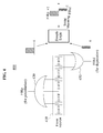
- FIG. 4 is a diagram illustrating an example of a pulse shaper circuit included in a neuromorphic system.
- the neuromorphic system may correspond to the neuromorphic system illustrated in FIG. 1 .
- a pulse shaper circuit may include only a portion of the structures illustrated in FIG. 4 .
- the pulse shaper circuit may form the shape of a neuron spike that is necessary for the STDP operation. That is, the pulse shaper circuit may generate a digital pulse indicating whether pulses corresponding to the spike fired by the neuron circuit are to potentiate or depress the synaptic weight of the synapse circuit.
- the pulse shaper circuit 400 includes a FIR filter 410, a first OR calculator 430, and a second OR calculator 450.
- the FIR filter 410 may be in the form of a 1-bit D flip-flop chain and be configured to store pulses transmitted from the neuron circuit.
- the first OR calculator 430 may generate the digital pulse by performing an OR calculation with respect to at least one pulse corresponding to potentiation of the synaptic weight among the pulses stored in the FIR filter 410.
- the second OR calculator 450 may generate the digital pulse by performing OR calculation with respect to at least one pulse that corresponds to depression of the synaptic weight among the pulses stored in the FIR filter 410.
- Output values of the first OR calculator 430 and the second OR calculator may express the synaptic weights of +1, 0, and -1 through simple calculation.
- the output value '1(+1)' of the first OR calculator 430 may refer to potentiation of the synaptic weight
- the output value '1(-1)' of the second OR calculator 450 may refer to depression of the synaptic weight.
- the output value of the first OR calculator 430 and the second OR calculator 450 is '0,' it may indicate no change to the synaptic network.
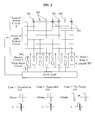
- FIG. 5 illustrates an example of a spike-timing dependent plasticity (STDP) operation method of a neuromorphic system.
- the neuromorphic system may correspond to the neuromorphic system illustrated in FIG. 1 .
- a WLx word line that corresponds to an axon of the neuron circuit A 509 is enabled at a falling edge of a pulse shaper signal. Further, pulse values of other neurons may be updated to the synapse circuit through the pulse shaper circuit.
- the IF when IF denotes a signal informing of firing of the neuron has and PS denotes a digital pulse shape generated by the pulse shaper circuit, the IF may have '1' or '0' as a pulse value generated in the pulse generator 330 of FIG. 3 .
- the PS may have a value of 1, -1, or 0. All neurons may each have its IF value and its PS value.
- the foregoing operation may be performed in the STDP logic circuit 507. Whether an update has occurred among a plurality of synapse circuits and updated values of the synapse circuits may be determined based on whether the digital pulses generated in the pulse shaper circuit potentiate or depress the synaptic weight.
- the STDP logic circuit 507 may determine update of the synapse circuits and the updated values, depending on a spike time between digital pulses corresponding to spikes fired by the plurality of neuron circuits.
- the STDP logic circuit 507 may determine an updated value of a synapse circuit that corresponds to a first neuron circuit, based on a second digital pulse value of a second neuron seen from the falling edge of a first digital pulse.
- the STDP logic circuit 507 may determine the updated value as a value for potentiating the synaptic weight. In the event that the second digital pulse precedes the first digital pulse, the STDP logic circuit 507 may determine the updated value as a value for depressing the synaptic weight.
- the STDP logic circuit 507 may determine to maintain the value of the synapse circuit corresponding to the first neuron circuit.
- the value of the second digital pulse of 'other' neuron circuits seen from the falling edge of the first digital pulse corresponding to the spike of the neuron circuit A 509 may occur later than that of the neuron circuit A 509.
- the value '+1' may be obtained when 'other' neuron circuits are seen from the falling edge of the first digital pulse.
- the value '+1' refers to potentiation of the synaptic weight.
- the value of the second digital pulse of 'other' neuron circuits seen from the falling edge of the first neuron corresponding to the spike of the neuron circuit A 509 may be earlier than the neuron circuit A 509, as in Case 2 shown by depression 530.
- the value '-1' may be obtained when 'other' neuron circuits are seen from the falling edge of the first digital pulse.
- the value '-1' refers to depression of the synaptic weight.
- '0' may be obtained as the value of the second digital pulse of 'other' neuron circuits seen from the falling edge of the first neuron corresponding to the spike of the neuron circuit A 509, as illustrated in Case 3 of no change 550.
- neurons corresponding to 505 among the axon lines of the neuron circuit A 509 are not changed at the falling edge of the neuron circuit A 509.
- the neuromorphic system may access the WLx line (refer to the WLx word line of FIG. 1 ) of the synapse circuit corresponding to the first neuron circuit at the falling edge of the first digital pulse corresponding to the fired spike, thereby enabling the WLx line.
- the STDP logic circuit 507 may determine whether an update of the synapse array occurred and the updated value, and access the WLx line (refer to the WLx word line of FIG. 1 ) of the synapse circuit to be updated through an encoder.
- the updated value of the corresponding synapse may be determined by C 1 C 0 output from the STDP logic circuit.
- a high integration and low-power neuromorphic system may be implemented, by flowing only a minor current equivalent to a leakage current to a neuron circuit and a synapse circuit constituting the neuromorphic system.
Landscapes
- Engineering & Computer Science (AREA)
- Physics & Mathematics (AREA)
- Health & Medical Sciences (AREA)
- Life Sciences & Earth Sciences (AREA)
- Theoretical Computer Science (AREA)
- Biomedical Technology (AREA)
- General Health & Medical Sciences (AREA)
- Biophysics (AREA)
- Molecular Biology (AREA)
- General Engineering & Computer Science (AREA)
- Evolutionary Computation (AREA)
- Data Mining & Analysis (AREA)
- Computing Systems (AREA)
- Computational Linguistics (AREA)
- General Physics & Mathematics (AREA)
- Mathematical Physics (AREA)
- Software Systems (AREA)
- Artificial Intelligence (AREA)
- Neurology (AREA)
- Computer Hardware Design (AREA)
- Semiconductor Memories (AREA)
- Static Random-Access Memory (AREA)
Applications Claiming Priority (2)
| Application Number | Priority Date | Filing Date | Title |
|---|---|---|---|
| KR20130065669 | 2013-06-10 | ||
| KR1020140016336A KR102382172B1 (ko) | 2013-06-10 | 2014-02-13 | 시냅스 어레이, 펄스 쉐이퍼 회로 및 이들을 포함하는 뉴로모픽 시스템 |
Publications (3)
| Publication Number | Publication Date |
|---|---|
| EP2814036A2 true EP2814036A2 (de) | 2014-12-17 |
| EP2814036A3 EP2814036A3 (de) | 2015-04-01 |
| EP2814036B1 EP2814036B1 (de) | 2020-07-08 |
Family
ID=50771443
Family Applications (1)
| Application Number | Title | Priority Date | Filing Date |
|---|---|---|---|
| EP14169845.6A Active EP2814036B1 (de) | 2013-06-10 | 2014-05-26 | Synapsen-Array, Impulsformungsschaltung und neuromorphes System |
Country Status (2)
| Country | Link |
|---|---|
| EP (1) | EP2814036B1 (de) |
| CN (1) | CN104240753B (de) |
Cited By (6)
| Publication number | Priority date | Publication date | Assignee | Title |
|---|---|---|---|---|
| CN109844772A (zh) * | 2016-11-09 | 2019-06-04 | 国际商业机器公司 | 存储器单元结构 |
| US10459724B2 (en) | 2016-01-18 | 2019-10-29 | Huawei Technologies Co., Ltd. | Memory device, and data processing method based on multi-layer RRAM crossbar array |
| CN111756352A (zh) * | 2020-05-18 | 2020-10-09 | 北京大学 | 脉冲阵列时域滤波方法、装置、设备及存储介质 |
| US11379714B2 (en) | 2018-05-29 | 2022-07-05 | British Cayman Islands Intelligo Technology Inc. | Architecture of in-memory computing memory device for use in artificial neuron |
| US11636883B2 (en) | 2016-03-18 | 2023-04-25 | Semiconductor Energy Laboratory Co., Ltd. | Semiconductor device and system using the same |
| US11893474B2 (en) | 2015-10-23 | 2024-02-06 | Semiconductor Energy Laboratory Co., Ltd. | Semiconductor device and electronic device |
Families Citing this family (13)
| Publication number | Priority date | Publication date | Assignee | Title |
|---|---|---|---|---|
| US10586147B2 (en) * | 2016-09-22 | 2020-03-10 | Intel Corporation | Neuromorphic computing device, memory device, system, and method to maintain a spike history for neurons in a neuromorphic computing environment |
| US11157805B2 (en) * | 2016-11-30 | 2021-10-26 | Japan Science And Technology Agency | Neuron circuit, system, and switch circuit |
| US10248906B2 (en) * | 2016-12-28 | 2019-04-02 | Intel Corporation | Neuromorphic circuits for storing and generating connectivity information |
| KR20180133061A (ko) | 2017-06-05 | 2018-12-13 | 에스케이하이닉스 주식회사 | 강유전체 전계 효과 트랜지스터들을 가진 시냅스들을 포함하는 뉴로모픽 소자의 시냅스 어레이 및 그 동작 방법 |
| CN107578096A (zh) * | 2017-09-21 | 2018-01-12 | 胡明建 | 一种压频式择端人工神经元的设计方法 |
| CN109829539A (zh) * | 2017-11-23 | 2019-05-31 | 旺宏电子股份有限公司 | 类神经计算装置 |
| CN111656371B (zh) * | 2018-01-23 | 2024-06-04 | 美商安纳富来希股份有限公司 | 具有非易失性突触阵列的神经网络电路 |
| US11586882B2 (en) | 2018-01-24 | 2023-02-21 | International Business Machines Corporation | Synapse memory |
| FR3081073B1 (fr) * | 2018-05-14 | 2021-10-08 | Univ Lille | Synapse artificielle commutee |
| CN109858619A (zh) * | 2019-01-22 | 2019-06-07 | 杭州电子科技大学 | 基于自旋振荡器的神经脉冲发生电路 |
| CN111325330B (zh) * | 2020-02-19 | 2022-10-11 | 北京大学 | 一种突触对称性时间依赖可塑性算法电路及其阵列结构 |
| CN115564032A (zh) * | 2021-07-02 | 2023-01-03 | 北京灵汐科技有限公司 | 逻辑门装置、处理核和众核系统 |
| CN115271052B (zh) * | 2022-03-28 | 2025-06-20 | 北京大学深圳研究生院 | 一种基于铁电场效应晶体管的电子突触电路及神经网络电路 |
Family Cites Families (11)
| Publication number | Priority date | Publication date | Assignee | Title |
|---|---|---|---|---|
| EP1182800B1 (de) * | 2000-08-24 | 2009-04-15 | Continental Automotive GmbH | Empfangssystem mit Antennendiversität |
| GB0203605D0 (en) * | 2002-02-15 | 2002-04-03 | Wood John | Hierarchical clocking system |
| TWI316787B (en) * | 2005-04-13 | 2009-11-01 | Via Tech Inc | Method for optimizing critical path timing in a logic synthesis flow and data processing system |
| US7292069B2 (en) * | 2005-12-30 | 2007-11-06 | Intel Corporation | Locally asynchronous, block-level synchronous, configurable logic blocks with sub-threshold analog circuits |
| CN101997538B (zh) * | 2009-08-19 | 2013-06-05 | 中国科学院半导体研究所 | 基于脉冲耦合的硅纳米线cmos神经元电路 |
| US9092736B2 (en) * | 2010-07-07 | 2015-07-28 | Qualcomm Incorporated | Communication and synapse training method and hardware for biologically inspired networks |
| US8473439B2 (en) * | 2010-12-08 | 2013-06-25 | International Business Machines Corporation | Integrate and fire electronic neurons |
| US8856055B2 (en) * | 2011-04-08 | 2014-10-07 | International Business Machines Corporation | Reconfigurable and customizable general-purpose circuits for neural networks |
| KR101888468B1 (ko) * | 2011-06-08 | 2018-08-16 | 삼성전자주식회사 | Stdp 기능 셀을 위한 시냅스, stdp 기능 셀 및 stdp 기능 셀을 이용한 뉴로모픽 회로 |
| CN102496385B (zh) * | 2011-12-26 | 2014-04-16 | 电子科技大学 | 一种脉冲时序活动性转换电路 |
| CN102610274B (zh) * | 2012-04-06 | 2014-10-15 | 电子科技大学 | 一种阻变突触权值调整电路 |
-
2014
- 2014-05-04 CN CN201410185178.8A patent/CN104240753B/zh active Active
- 2014-05-26 EP EP14169845.6A patent/EP2814036B1/de active Active
Non-Patent Citations (1)
| Title |
|---|
| None |
Cited By (7)
| Publication number | Priority date | Publication date | Assignee | Title |
|---|---|---|---|---|
| US11893474B2 (en) | 2015-10-23 | 2024-02-06 | Semiconductor Energy Laboratory Co., Ltd. | Semiconductor device and electronic device |
| US12387093B2 (en) | 2015-10-23 | 2025-08-12 | Semiconductor Energy Laboratory Co., Ltd. | Semiconductor device and electronic device |
| US10459724B2 (en) | 2016-01-18 | 2019-10-29 | Huawei Technologies Co., Ltd. | Memory device, and data processing method based on multi-layer RRAM crossbar array |
| US11636883B2 (en) | 2016-03-18 | 2023-04-25 | Semiconductor Energy Laboratory Co., Ltd. | Semiconductor device and system using the same |
| CN109844772A (zh) * | 2016-11-09 | 2019-06-04 | 国际商业机器公司 | 存储器单元结构 |
| US11379714B2 (en) | 2018-05-29 | 2022-07-05 | British Cayman Islands Intelligo Technology Inc. | Architecture of in-memory computing memory device for use in artificial neuron |
| CN111756352A (zh) * | 2020-05-18 | 2020-10-09 | 北京大学 | 脉冲阵列时域滤波方法、装置、设备及存储介质 |
Also Published As
| Publication number | Publication date |
|---|---|
| CN104240753B (zh) | 2018-08-28 |
| CN104240753A (zh) | 2014-12-24 |
| EP2814036A3 (de) | 2015-04-01 |
| EP2814036B1 (de) | 2020-07-08 |
Similar Documents
| Publication | Publication Date | Title |
|---|---|---|
| US9418333B2 (en) | Synapse array, pulse shaper circuit and neuromorphic system | |
| EP2814036B1 (de) | Synapsen-Array, Impulsformungsschaltung und neuromorphes System | |
| TWI503761B (zh) | 用於在脈波編碼的網路中的突觸更新的裝置和方法 | |
| CN105229675B (zh) | 尖峰网络的高效硬件实现 | |
| US9805302B2 (en) | Synapse circuit and neuromorphic system including the same | |
| US9466362B2 (en) | Resistive cross-point architecture for robust data representation with arbitrary precision | |
| US8725662B2 (en) | Apparatus and method for partial evaluation of synaptic updates based on system events | |
| CN114897143B (zh) | 神经元单元电路、脉冲神经网络及智能物联网芯片 | |
| US20240005162A1 (en) | Error-triggered learning of multi-layer memristive spiking neural networks | |
| CN102610274A (zh) | 一种阻变突触权值调整电路 | |
| US20120011093A1 (en) | Methods and systems for digital neural processing with discrete-level synapes and probabilistic stdp | |
| CN105934766A (zh) | 用阴影网络来监视神经网络 | |
| CN106164940A (zh) | 在尖峰神经网络中通过全局标量值来调制可塑性 | |
| Wang et al. | A mixed-signal implementation of a polychronous spiking neural network with delay adaptation | |
| KR20200060204A (ko) | 조건적 바이어스 전류에 의해 작동되는 비교기를 포함하는 스파이크 뉴럴 네트워크 회로 | |
| US11861483B2 (en) | Spike neural network circuit including comparator operated by conditional bias current | |
| Kim et al. | 29.1 A 32.5 mW mixed-signal processing-in-memory-based k-SAT solver in 65nm CMOS with 74.0% solvability for 30-variable 126-clause 3-SAT problems | |
| Oshio et al. | A memcapacitive spiking neural network with circuit nonlinearity-aware training | |
| CN105659260A (zh) | 动态地指派和检查突触延迟 | |
| JP2024123529A (ja) | ニューラルネットワーク装置およびシナプス重み更新方法 | |
| Babu et al. | Stochastic deep learning in memristive networks | |
| Luo et al. | A mixed-signal spiking neuromorphic architecture for scalable neural network | |
| WO2015148060A2 (en) | Time synchronization of spiking neuron models on multiple nodes | |
| Vincent | Analog Spiking Neural Network Implementing Spike Timing-Dependent Plasticity on 65 nm CMOS | |
| Ying et al. | A scalable hardware architecture for multi-layer spiking neural networks |
Legal Events
| Date | Code | Title | Description |
|---|---|---|---|
| 17P | Request for examination filed |
Effective date: 20140526 |
|
| AK | Designated contracting states |
Kind code of ref document: A2 Designated state(s): AL AT BE BG CH CY CZ DE DK EE ES FI FR GB GR HR HU IE IS IT LI LT LU LV MC MK MT NL NO PL PT RO RS SE SI SK SM TR |
|
| AX | Request for extension of the european patent |
Extension state: BA ME |
|
| PUAI | Public reference made under article 153(3) epc to a published international application that has entered the european phase |
Free format text: ORIGINAL CODE: 0009012 |
|
| PUAL | Search report despatched |
Free format text: ORIGINAL CODE: 0009013 |
|
| AK | Designated contracting states |
Kind code of ref document: A3 Designated state(s): AL AT BE BG CH CY CZ DE DK EE ES FI FR GB GR HR HU IE IS IT LI LT LU LV MC MK MT NL NO PL PT RO RS SE SI SK SM TR |
|
| AX | Request for extension of the european patent |
Extension state: BA ME |
|
| RIC1 | Information provided on ipc code assigned before grant |
Ipc: G06N 3/04 20060101ALI20150223BHEP Ipc: G06N 3/063 20060101ALI20150223BHEP Ipc: G11C 11/54 20060101AFI20150223BHEP |
|
| R17P | Request for examination filed (corrected) |
Effective date: 20151001 |
|
| RBV | Designated contracting states (corrected) |
Designated state(s): AL AT BE BG CH CY CZ DE DK EE ES FI FR GB GR HR HU IE IS IT LI LT LU LV MC MK MT NL NO PL PT RO RS SE SI SK SM TR |
|
| STAA | Information on the status of an ep patent application or granted ep patent |
Free format text: STATUS: EXAMINATION IS IN PROGRESS |
|
| 17Q | First examination report despatched |
Effective date: 20190724 |
|
| GRAP | Despatch of communication of intention to grant a patent |
Free format text: ORIGINAL CODE: EPIDOSNIGR1 |
|
| STAA | Information on the status of an ep patent application or granted ep patent |
Free format text: STATUS: GRANT OF PATENT IS INTENDED |
|
| INTG | Intention to grant announced |
Effective date: 20200203 |
|
| GRAS | Grant fee paid |
Free format text: ORIGINAL CODE: EPIDOSNIGR3 |
|
| GRAA | (expected) grant |
Free format text: ORIGINAL CODE: 0009210 |
|
| STAA | Information on the status of an ep patent application or granted ep patent |
Free format text: STATUS: THE PATENT HAS BEEN GRANTED |
|
| AK | Designated contracting states |
Kind code of ref document: B1 Designated state(s): AL AT BE BG CH CY CZ DE DK EE ES FI FR GB GR HR HU IE IS IT LI LT LU LV MC MK MT NL NO PL PT RO RS SE SI SK SM TR |
|
| REG | Reference to a national code |
Ref country code: AT Ref legal event code: REF Ref document number: 1289333 Country of ref document: AT Kind code of ref document: T Effective date: 20200715 Ref country code: CH Ref legal event code: EP |
|
| REG | Reference to a national code |
Ref country code: DE Ref legal event code: R096 Ref document number: 602014067423 Country of ref document: DE |
|
| REG | Reference to a national code |
Ref country code: IE Ref legal event code: FG4D |
|
| REG | Reference to a national code |
Ref country code: LT Ref legal event code: MG4D |
|
| REG | Reference to a national code |
Ref country code: AT Ref legal event code: MK05 Ref document number: 1289333 Country of ref document: AT Kind code of ref document: T Effective date: 20200708 |
|
| REG | Reference to a national code |
Ref country code: NL Ref legal event code: MP Effective date: 20200708 |
|
| PG25 | Lapsed in a contracting state [announced via postgrant information from national office to epo] |
Ref country code: AT Free format text: LAPSE BECAUSE OF FAILURE TO SUBMIT A TRANSLATION OF THE DESCRIPTION OR TO PAY THE FEE WITHIN THE PRESCRIBED TIME-LIMIT Effective date: 20200708 Ref country code: PT Free format text: LAPSE BECAUSE OF FAILURE TO SUBMIT A TRANSLATION OF THE DESCRIPTION OR TO PAY THE FEE WITHIN THE PRESCRIBED TIME-LIMIT Effective date: 20201109 Ref country code: BG Free format text: LAPSE BECAUSE OF FAILURE TO SUBMIT A TRANSLATION OF THE DESCRIPTION OR TO PAY THE FEE WITHIN THE PRESCRIBED TIME-LIMIT Effective date: 20201008 Ref country code: SE Free format text: LAPSE BECAUSE OF FAILURE TO SUBMIT A TRANSLATION OF THE DESCRIPTION OR TO PAY THE FEE WITHIN THE PRESCRIBED TIME-LIMIT Effective date: 20200708 Ref country code: GR Free format text: LAPSE BECAUSE OF FAILURE TO SUBMIT A TRANSLATION OF THE DESCRIPTION OR TO PAY THE FEE WITHIN THE PRESCRIBED TIME-LIMIT Effective date: 20201009 Ref country code: ES Free format text: LAPSE BECAUSE OF FAILURE TO SUBMIT A TRANSLATION OF THE DESCRIPTION OR TO PAY THE FEE WITHIN THE PRESCRIBED TIME-LIMIT Effective date: 20200708 Ref country code: NO Free format text: LAPSE BECAUSE OF FAILURE TO SUBMIT A TRANSLATION OF THE DESCRIPTION OR TO PAY THE FEE WITHIN THE PRESCRIBED TIME-LIMIT Effective date: 20201008 Ref country code: LT Free format text: LAPSE BECAUSE OF FAILURE TO SUBMIT A TRANSLATION OF THE DESCRIPTION OR TO PAY THE FEE WITHIN THE PRESCRIBED TIME-LIMIT Effective date: 20200708 Ref country code: HR Free format text: LAPSE BECAUSE OF FAILURE TO SUBMIT A TRANSLATION OF THE DESCRIPTION OR TO PAY THE FEE WITHIN THE PRESCRIBED TIME-LIMIT Effective date: 20200708 Ref country code: FI Free format text: LAPSE BECAUSE OF FAILURE TO SUBMIT A TRANSLATION OF THE DESCRIPTION OR TO PAY THE FEE WITHIN THE PRESCRIBED TIME-LIMIT Effective date: 20200708 |
|
| PG25 | Lapsed in a contracting state [announced via postgrant information from national office to epo] |
Ref country code: IS Free format text: LAPSE BECAUSE OF FAILURE TO SUBMIT A TRANSLATION OF THE DESCRIPTION OR TO PAY THE FEE WITHIN THE PRESCRIBED TIME-LIMIT Effective date: 20201108 Ref country code: LV Free format text: LAPSE BECAUSE OF FAILURE TO SUBMIT A TRANSLATION OF THE DESCRIPTION OR TO PAY THE FEE WITHIN THE PRESCRIBED TIME-LIMIT Effective date: 20200708 Ref country code: PL Free format text: LAPSE BECAUSE OF FAILURE TO SUBMIT A TRANSLATION OF THE DESCRIPTION OR TO PAY THE FEE WITHIN THE PRESCRIBED TIME-LIMIT Effective date: 20200708 Ref country code: RS Free format text: LAPSE BECAUSE OF FAILURE TO SUBMIT A TRANSLATION OF THE DESCRIPTION OR TO PAY THE FEE WITHIN THE PRESCRIBED TIME-LIMIT Effective date: 20200708 |
|
| PG25 | Lapsed in a contracting state [announced via postgrant information from national office to epo] |
Ref country code: NL Free format text: LAPSE BECAUSE OF FAILURE TO SUBMIT A TRANSLATION OF THE DESCRIPTION OR TO PAY THE FEE WITHIN THE PRESCRIBED TIME-LIMIT Effective date: 20200708 |
|
| REG | Reference to a national code |
Ref country code: DE Ref legal event code: R097 Ref document number: 602014067423 Country of ref document: DE |
|
| PG25 | Lapsed in a contracting state [announced via postgrant information from national office to epo] |
Ref country code: SM Free format text: LAPSE BECAUSE OF FAILURE TO SUBMIT A TRANSLATION OF THE DESCRIPTION OR TO PAY THE FEE WITHIN THE PRESCRIBED TIME-LIMIT Effective date: 20200708 Ref country code: RO Free format text: LAPSE BECAUSE OF FAILURE TO SUBMIT A TRANSLATION OF THE DESCRIPTION OR TO PAY THE FEE WITHIN THE PRESCRIBED TIME-LIMIT Effective date: 20200708 Ref country code: IT Free format text: LAPSE BECAUSE OF FAILURE TO SUBMIT A TRANSLATION OF THE DESCRIPTION OR TO PAY THE FEE WITHIN THE PRESCRIBED TIME-LIMIT Effective date: 20200708 Ref country code: EE Free format text: LAPSE BECAUSE OF FAILURE TO SUBMIT A TRANSLATION OF THE DESCRIPTION OR TO PAY THE FEE WITHIN THE PRESCRIBED TIME-LIMIT Effective date: 20200708 Ref country code: CZ Free format text: LAPSE BECAUSE OF FAILURE TO SUBMIT A TRANSLATION OF THE DESCRIPTION OR TO PAY THE FEE WITHIN THE PRESCRIBED TIME-LIMIT Effective date: 20200708 Ref country code: DK Free format text: LAPSE BECAUSE OF FAILURE TO SUBMIT A TRANSLATION OF THE DESCRIPTION OR TO PAY THE FEE WITHIN THE PRESCRIBED TIME-LIMIT Effective date: 20200708 |
|
| PLBE | No opposition filed within time limit |
Free format text: ORIGINAL CODE: 0009261 |
|
| STAA | Information on the status of an ep patent application or granted ep patent |
Free format text: STATUS: NO OPPOSITION FILED WITHIN TIME LIMIT |
|
| PG25 | Lapsed in a contracting state [announced via postgrant information from national office to epo] |
Ref country code: AL Free format text: LAPSE BECAUSE OF FAILURE TO SUBMIT A TRANSLATION OF THE DESCRIPTION OR TO PAY THE FEE WITHIN THE PRESCRIBED TIME-LIMIT Effective date: 20200708 |
|
| 26N | No opposition filed |
Effective date: 20210409 |
|
| PG25 | Lapsed in a contracting state [announced via postgrant information from national office to epo] |
Ref country code: SK Free format text: LAPSE BECAUSE OF FAILURE TO SUBMIT A TRANSLATION OF THE DESCRIPTION OR TO PAY THE FEE WITHIN THE PRESCRIBED TIME-LIMIT Effective date: 20200708 |
|
| PG25 | Lapsed in a contracting state [announced via postgrant information from national office to epo] |
Ref country code: SI Free format text: LAPSE BECAUSE OF FAILURE TO SUBMIT A TRANSLATION OF THE DESCRIPTION OR TO PAY THE FEE WITHIN THE PRESCRIBED TIME-LIMIT Effective date: 20200708 |
|
| REG | Reference to a national code |
Ref country code: CH Ref legal event code: PL |
|
| PG25 | Lapsed in a contracting state [announced via postgrant information from national office to epo] |
Ref country code: LU Free format text: LAPSE BECAUSE OF NON-PAYMENT OF DUE FEES Effective date: 20210526 Ref country code: MC Free format text: LAPSE BECAUSE OF FAILURE TO SUBMIT A TRANSLATION OF THE DESCRIPTION OR TO PAY THE FEE WITHIN THE PRESCRIBED TIME-LIMIT Effective date: 20200708 Ref country code: LI Free format text: LAPSE BECAUSE OF NON-PAYMENT OF DUE FEES Effective date: 20210531 Ref country code: CH Free format text: LAPSE BECAUSE OF NON-PAYMENT OF DUE FEES Effective date: 20210531 |
|
| REG | Reference to a national code |
Ref country code: BE Ref legal event code: MM Effective date: 20210531 |
|
| PG25 | Lapsed in a contracting state [announced via postgrant information from national office to epo] |
Ref country code: IE Free format text: LAPSE BECAUSE OF NON-PAYMENT OF DUE FEES Effective date: 20210526 |
|
| PG25 | Lapsed in a contracting state [announced via postgrant information from national office to epo] |
Ref country code: BE Free format text: LAPSE BECAUSE OF NON-PAYMENT OF DUE FEES Effective date: 20210531 |
|
| PG25 | Lapsed in a contracting state [announced via postgrant information from national office to epo] |
Ref country code: HU Free format text: LAPSE BECAUSE OF FAILURE TO SUBMIT A TRANSLATION OF THE DESCRIPTION OR TO PAY THE FEE WITHIN THE PRESCRIBED TIME-LIMIT; INVALID AB INITIO Effective date: 20140526 |
|
| PG25 | Lapsed in a contracting state [announced via postgrant information from national office to epo] |
Ref country code: CY Free format text: LAPSE BECAUSE OF FAILURE TO SUBMIT A TRANSLATION OF THE DESCRIPTION OR TO PAY THE FEE WITHIN THE PRESCRIBED TIME-LIMIT Effective date: 20200708 |
|
| P01 | Opt-out of the competence of the unified patent court (upc) registered |
Effective date: 20230530 |
|
| PG25 | Lapsed in a contracting state [announced via postgrant information from national office to epo] |
Ref country code: MK Free format text: LAPSE BECAUSE OF FAILURE TO SUBMIT A TRANSLATION OF THE DESCRIPTION OR TO PAY THE FEE WITHIN THE PRESCRIBED TIME-LIMIT Effective date: 20200708 |
|
| PG25 | Lapsed in a contracting state [announced via postgrant information from national office to epo] |
Ref country code: TR Free format text: LAPSE BECAUSE OF FAILURE TO SUBMIT A TRANSLATION OF THE DESCRIPTION OR TO PAY THE FEE WITHIN THE PRESCRIBED TIME-LIMIT Effective date: 20200708 |
|
| PG25 | Lapsed in a contracting state [announced via postgrant information from national office to epo] |
Ref country code: MT Free format text: LAPSE BECAUSE OF FAILURE TO SUBMIT A TRANSLATION OF THE DESCRIPTION OR TO PAY THE FEE WITHIN THE PRESCRIBED TIME-LIMIT Effective date: 20200708 |
|
| PGFP | Annual fee paid to national office [announced via postgrant information from national office to epo] |
Ref country code: DE Payment date: 20250408 Year of fee payment: 12 |
|
| PGFP | Annual fee paid to national office [announced via postgrant information from national office to epo] |
Ref country code: FR Payment date: 20250409 Year of fee payment: 12 |
|
| PGFP | Annual fee paid to national office [announced via postgrant information from national office to epo] |
Ref country code: GB Payment date: 20260323 Year of fee payment: 13 |