EP2814036A2 - Synapse array, pulse shaper circuit and neuromorphic system - Google Patents
Synapse array, pulse shaper circuit and neuromorphic system Download PDFInfo
- Publication number
- EP2814036A2 EP2814036A2 EP14169845.6A EP14169845A EP2814036A2 EP 2814036 A2 EP2814036 A2 EP 2814036A2 EP 14169845 A EP14169845 A EP 14169845A EP 2814036 A2 EP2814036 A2 EP 2814036A2
- Authority
- EP
- European Patent Office
- Prior art keywords
- circuit
- synapse
- neuron
- pulse
- circuits
- Prior art date
- Legal status (The legal status is an assumption and is not a legal conclusion. Google has not performed a legal analysis and makes no representation as to the accuracy of the status listed.)
- Granted
Links
- 210000000225 synapse Anatomy 0.000 title claims abstract description 134
- 210000002569 neuron Anatomy 0.000 claims abstract description 143
- 239000012528 membrane Substances 0.000 claims abstract description 31
- 230000003068 static effect Effects 0.000 claims abstract description 5
- 230000000946 synaptic effect Effects 0.000 claims description 42
- 230000010355 oscillation Effects 0.000 claims description 20
- 238000010304 firing Methods 0.000 claims description 12
- 230000004044 response Effects 0.000 claims description 12
- 230000003389 potentiating effect Effects 0.000 claims description 10
- 230000008859 change Effects 0.000 claims description 8
- 230000001419 dependent effect Effects 0.000 claims description 5
- 241001290721 Odontonema tubiforme Species 0.000 claims description 4
- 230000003213 activating effect Effects 0.000 claims description 3
- 230000000881 depressing effect Effects 0.000 claims description 3
- 238000000034 method Methods 0.000 description 9
- 210000003050 axon Anatomy 0.000 description 7
- 238000010586 diagram Methods 0.000 description 6
- 230000010354 integration Effects 0.000 description 5
- 230000001242 postsynaptic effect Effects 0.000 description 4
- 239000004065 semiconductor Substances 0.000 description 4
- 230000005540 biological transmission Effects 0.000 description 3
- 210000000653 nervous system Anatomy 0.000 description 3
- 210000005215 presynaptic neuron Anatomy 0.000 description 3
- 230000008569 process Effects 0.000 description 3
- 210000004556 brain Anatomy 0.000 description 2
- 230000006870 function Effects 0.000 description 2
- 229910044991 metal oxide Inorganic materials 0.000 description 2
- 210000005036 nerve Anatomy 0.000 description 2
- 230000002411 adverse Effects 0.000 description 1
- 238000003491 array Methods 0.000 description 1
- 230000001413 cellular effect Effects 0.000 description 1
- 230000000295 complement effect Effects 0.000 description 1
- 238000010276 construction Methods 0.000 description 1
- 210000001787 dendrite Anatomy 0.000 description 1
- 230000000994 depressogenic effect Effects 0.000 description 1
- 230000000694 effects Effects 0.000 description 1
- 238000004519 manufacturing process Methods 0.000 description 1
- 230000007246 mechanism Effects 0.000 description 1
- 150000004706 metal oxides Chemical class 0.000 description 1
- 230000003278 mimic effect Effects 0.000 description 1
- 238000012986 modification Methods 0.000 description 1
- 230000004048 modification Effects 0.000 description 1
- 230000001537 neural effect Effects 0.000 description 1
- 230000003518 presynaptic effect Effects 0.000 description 1
- 238000003672 processing method Methods 0.000 description 1
- 230000009467 reduction Effects 0.000 description 1
- 230000000638 stimulation Effects 0.000 description 1
Images


Classifications
-
- G—PHYSICS
- G11—INFORMATION STORAGE
- G11C—STATIC STORES
- G11C11/00—Digital stores characterised by the use of particular electric or magnetic storage elements; Storage elements therefor
- G11C11/54—Digital stores characterised by the use of particular electric or magnetic storage elements; Storage elements therefor using elements simulating biological cells, e.g. neuron
-
- G—PHYSICS
- G06—COMPUTING; CALCULATING OR COUNTING
- G06N—COMPUTING ARRANGEMENTS BASED ON SPECIFIC COMPUTATIONAL MODELS
- G06N3/00—Computing arrangements based on biological models
- G06N3/02—Neural networks
- G06N3/04—Architecture, e.g. interconnection topology
- G06N3/049—Temporal neural networks, e.g. delay elements, oscillating neurons or pulsed inputs
-
- G—PHYSICS
- G06—COMPUTING; CALCULATING OR COUNTING
- G06N—COMPUTING ARRANGEMENTS BASED ON SPECIFIC COMPUTATIONAL MODELS
- G06N3/00—Computing arrangements based on biological models
- G06N3/02—Neural networks
- G06N3/06—Physical realisation, i.e. hardware implementation of neural networks, neurons or parts of neurons
- G06N3/063—Physical realisation, i.e. hardware implementation of neural networks, neurons or parts of neurons using electronic means
Definitions
- the following description relates to a synapse array, a pulse shaper circuit, and a neuromorphic system that includes a synapse array and/or a pulse shaper circuit.
- a physiological brain includes hundreds of billions of neurons that are interconnected with one another in a complicated nerve network. Neurons are considered to be responsible for the intellectual capability for learning and memory. In the cellular level, neurons use their synapses to exchange signals with thousands of other neurons. Thus, the neurons may be considered the structural and functional base units for data transmission.
- a synapse refers to a junction between two neurons at which an axon of a first neuron and a dendrite of a second neuron are positioned next to each other for transmission of data.
- a single neuron is generally connected with thousands of other neurons via synapses.
- a data processing method of the brain may be mimicked to achieve a new data processing and storing method.
- a neuromorphic system refers to a semiconductor circuit that is designed to mimic the operation of the biological nervous system.
- a neuromorphic system may be used in a variety of applications, including in the implementation of an intelligent system that is capable of adapting itself to an unspecified environment.
- a synapse array based on a static random access memory (SRAM), the synapse array including a plurality of synapse circuits, in which at least one synapse circuit among the plurality of synapse circuits includes at least one bias transistor and at least two cut-off transistors, and the at least one synapse circuit is configured to charge a membrane node of a neuron circuit connected with the at least one synapse circuit using a sub-threshold leakage current that passed through the at least one bias transistor.
- SRAM static random access memory
- the at least one synapse circuit may be configured to change a value of the SRAM using a leakage current that passed through the at least two cut-off transistors.
- the neuron circuit may be configured to fire a spike based on a result of comparing a number of occurrences of oscillation pulses generated based on a voltage of the membrane node to a predetermined reference number.
- the neuron circuit may include: a pulse generator configured to generate an oscillation pulse based on a voltage of the membrane node; a counter configured to count a number of occurrences of the oscillation pulse; and a comparator configured to compare the number of occurrences to a predetermined reference number.
- the comparator may be configured to compare the reference number with the number of occurrences, in synchronization with a clock signal periodically input.
- the neuron circuit may further include a transistor connected to a ground.
- the oscillation pulse may be used to reset the membrane node by activating the transistor.
- the at least two cut-off transistors may include a first cut-off transistor and a second cut-off transistor.
- the first cut-off transistor may be connected to a power voltage for pull-up.
- the second cut-off transistor may be connected to a ground for pull-down.
- the at least one bias transistor may be connected to the membrane node of the neuron circuit connected with the at least one synapse circuit.
- a pulse shaper circuit that is configured to generate a digital pulse indicating whether pulses corresponding to spikes fired by a neuron circuit potentiate or depress a synaptic weight of a synapse circuit.
- the general aspect of the pulse shaper circuit may further include: a finite impulse response (FIR) filter comprising a 1-bit D flip flop chain configured to store the pulses; a first OR calculator configured to generate the digital pulse by performing OR calculation with respect to at least one pulse corresponding to potentiation of the synaptic weight among the stored pulses; and a second OR calculator is configured to generate the digital pulse by performing OR calculation with respect to at least one pulse corresponding to depression of the synaptic weight among the stored pulses.
- FIR finite impulse response
- the pulse shaper circuit may be configured to generate the digital pulse for maintaining the synaptic weight based on a value of the first OR calculator and a value of the second OR calculator.
- a neuromorphic system including: a synapse array based on a SRAM, the synapse array including at least one synapse circuit; a neuron circuit connected with the synapse circuit, the synapse circuit being configured to charge a membrane node of the neuron circuit using a sub-threshold leakage current that passed through at least one bias transistor of the synapse array, and the neuron circuit being configured to fire spikes based on a voltage of the membrane node; and a pulse shaper circuit configured to generate a digital pulse corresponding to the fired spikes.
- the synapse array may include a plurality of synapse circuits, the plurality of synapse circuits including the at least one synapse circuit.
- the neuromorphic system may include a plurality of neuron circuits and a plurality of pulse shaper circuits.
- the neuromorphic system may further include a spike-timing dependent plasticity (STDP) logic circuit configured to determine an update state of a synapse circuit among the plurality of synapse circuits and an updated value for the synapse circuit based on the digital pulse, and an encoder configured to access a synapse circuit to be updated according to the digital pulse.
- STDP spike-timing dependent plasticity
- the neuron circuit may be configured to fire spikes based on a result of comparing a number of occurrences of oscillation pulses generated based on the voltage of the membrane node to a predetermined reference number.
- the synapse array may further include at least two cut-off transistors, and may be configured to change a value of the SRAM using a leakage current that passed through the at least two cut-off transistors.
- the neuron circuit may include: a pulse generation unit configured to generate an oscillation pulse based on a voltage of the membrane node; a counter configured to count a number of occurrences of the oscillation pulse; and a comparator configured to compare the number of occurrences to a predetermined reference number.
- the neuron circuit may further include a transistor connected to a ground.
- the oscillation pulse may be used to reset the membrane node by activating the transistor.
- the at least two cut-off transistors may include a first cut-off transistor and a second cut-off transistor.
- the first cut-off transistor may be connected to a power voltage for pull-up.
- the second cut-off transistor may be connected to a ground for pull-down.
- the at least one bias transistor may be connected to the membrane node of the neuron circuit connected with the synapse circuit.
- the pulse shaper circuits may be configured to generate a digital pulse indicating whether pulses corresponding to spikes fired by a neuron circuit potentiate or depress a synaptic weight of the synapse circuit.
- the STDP logic circuit may be configured to determine an update state of the plurality of synapse circuits and an updated value for the synapse circuits based on whether the digital pulse potentiates or depresses the synaptic weight.
- the STDP logic circuit may be configured to determine the update state and the updated value of the synapse circuits, depending on a spike time between digital pulses corresponding to the spikes fired by the plurality of neuron circuits.
- the neuromorphic system may be configured to enable a write line (WL) of a synapse circuit corresponding to a first neuron circuit at a falling edge of a first digital pulse corresponding to a spike fired by the first neuron circuit in response to the first neuron circuit among the plurality of neuron circuits firing the spike.
- WL write line
- the STDP logic circuit may be configured to determine the updated value of the synapse circuit corresponding to the first neuron circuit based on a value of a second digital pulse of a second neuron seen from the falling edge of the first digital pulse.
- the STDP logic circuit may be configured to update a value for potentiating the synaptic weight as the updated value in response to the first digital pulse preceding the second digital pulse.
- the STDP logic circuit may be configured to update a value for depressing the synaptic weight as the updated value in response to the second digital pulse preceding the first digital pulse.
- the STDP logic circuit may be configured to determine to maintain the value of the synapse circuit corresponding to the first neuron circuit in response to '0' being detected at the falling edge of the first digital pulse.
- the encoder may be configured to transmit the updated value to the synapse circuits according to the digital pulse.
- FIG. 1 illustrates an overall structure of an example of a neuromorphic system 100.
- the neuromorphic system 100 includes a static random access memory (SRAM)-based synapse array 110, a plurality of neuron circuits 130, a plurality of pulse shaper circuits 150, a spike-timing dependent plasticity (STDP) logic circuit 170, and an encoder 190.
- SRAM static random access memory
- STDP spike-timing dependent plasticity
- a neuromorphic system may include one or more of the SRAM-based synapse array, neurons circuits, pulse shaper circuits, STDP logic circuit and encoder, without including all of these structures.
- the SRAM-based synapse array 110 includes a plurality of synapse circuits based on an SRAM structure.
- Each of the synapse circuits may include at least one bias transistor and at least two cut-off transistors.
- the synapse circuit may charge membrane nodes of the neuron circuits 130 that is connected with the synapse circuit, using a sub-threshold leakage current that passed through the at least one bias transistor.
- the synapse circuit may change a value of the SRAM by using a leakage current that passes through the at least two cut-off transistors.
- the synapse circuit may include the at least two cut-off transistors, for example, a first cut-off transistor and a second cut-off transistor.
- the first cut-off transistor may be connected to a voltage drain drain (VDD) for pull-up.
- the second cut-off transistor may be connected to a ground (GND) for pull-down.
- the at least one bias transistor may be connected to the membrane nodes of the neuron circuits 130 that is connected to the synapse circuit.
- WLx/WLxB indicated at the synapse array 110 refers to a word line, that is, a line for selecting an address of an axon.
- x refers to an order of each line.
- x may be a natural number ranging from 0 to 3.
- a logic value of WLx of the synapse array 110 is 1.
- an STDP result may be used for the SRAM through C 1 C 0 x, that is, STDP information of each neuron transmitted through an STDP logic circuit.
- STDP refers to a learning mechanism postulated to exist in synapses of biological nerve networks.
- synaptic efficacy or weight is slightly altered between two neurons based on information such as the timing of a pre-synaptic spike in a pre-synaptic neuron and a post-synaptic spike in a post-synaptic neuron. That is, a synaptic circuit may be potentiated or depressed to change the efficacy of data transmission between two neurons.
- the operation and configuration of an example of the synapse circuit are further described below with reference to FIG. 2 .
- the plurality of neuron circuits 130 may fire spikes based on a result of comparing a number of occurrences of oscillation pulses generated on the basis of an input voltage input from the membrane nodes, to a predetermined reference number.
- An example of the neuron circuit 130 is further described below with reference to FIG. 3 .
- the plurality of pulse shaper circuits 150 may receive a signal transmitted from the neuron circuit 130, and may generate a pulse for the STDP operation based on the signal.
- the pulse shaper circuits 150 may generate digital pulses corresponding to the spikes fired at the neuron circuits 130.
- the pulse shaper circuits 150 may generate the digital pulses that indicate whether pulses corresponding to the fired spikes potentiate (strengthen) or depress (weaken) a synaptic weight of the synapse circuit.
- An example of the pulse shaper circuit 150 is further described below with reference to FIG. 4 .
- the STDP logic circuit 170 may receive the signal generated by the pulse shaper circuits 150, and may perform the STDP operation based on the signal. That is, the STDP logic circuit 170 may determine an update state of the plurality of synapse circuits and updated values for the synapse circuits, based on the digital pulses generated by the pulse shaper circuits 150.
- the STDP logic circuit 170 may include an address event representation (AER) function, by which the STDP logic circuit 170 may transmit a test result related to the neuron circuits 130 and information regarding firing generated in a random neuron circuit 130 to other neuron circuits 130.
- the updated value determined by the STDP logic circuit 170 may be transmitted to the synapse array 110 through the WBLx line.
- the STDP logic circuit 170 may determine the presence of absence of an updating event (update state) and the updated values of the synapse circuits, based on a spike time between the digital pulses corresponding to the spikes fired by the plurality of neuron circuits 130.
- the operation of the STDP logic circuit 170 is further described below with reference to FIG. 5 .
- the encoder 190 may access the synapse array 110 according to the digital pulses generated by the pulse shapers 150.
- the encoder 190 may access the synapse arrays to be updated according to the digital pulses, or transmit the updated values to the synapse circuits according to the digital pulses. For example, in the event that a firing occurred in a neuron circuit 130, the pulse generated at a pulse shaper circuit 150, for example '1', may be transmitted to the encoder 190.
- the encoder 190 may transmit a logic value '1' to WLO to update the synaptic weight of the synapse circuit corresponding to the neuron circuit 130.
- the WLO line refers to a line for selecting the address of a word line. That is, the WLO line (or other WLx line) may correspond to a Write Enable state.
- states of the synapse circuits corresponding to a first word line for example, corresponding to an axon of neuron circuit A in FIG. 5 may be the Write Enable state.
- the encoder 190 does not transmit the pulse and, in this state, the logic value '0' may be applied to WL2. Therefore, synapse circuits corresponding to a third word line may be in a Write Disable state and data may not be written.
- the neuromorphic system may enable a write line, for example the WLX line, of the synapse circuit corresponding to the first neuron circuit in a falling edge of a first digital pulse corresponding to the fired spike.
- the neuromorphic system may be greatly affected by a leakage current of devices, a mismatch between devices, and a process voltage temperature (PVT) variation.
- PVT process voltage temperature
- CMOS complementary metal oxide semiconductor
- the leakage current from semiconductor components may further increase. The increase in leakage current may potentially cause continuous firings inside a neuron circuit even when no external stimulation is applied to the neuron circuit.
- leakage current has been considered an adverse side effect in designing a neuromorphic system.
- the neuromorphic system may be implemented in such a way that it meets the demand for high integration and low power, by using a small amount of current equivalent to the amount of leakage current.
- FIG. 2 illustrates an example of a synapse circuit 200 included in a neuromorphic system.
- the neuromorphic system may correspond to the neuromorphic system illustrated in FIG. 1 .
- a synapse circuit may include only a portion of the structures illustrated in FIG. 2 .
- the synapse circuit 200 includes at least two cut-off transistors 210 and 230, and at least one bias transistor 260.
- the synapse circuit 200 is configured to charge a membrane node of a neuron circuit connected with the synapse circuit 200, using a sub-threshold leakage current that passed through the at least one bias transistor 260.
- the at least two cut-off transistors 210 and 230 include a first cut-off transistor 210 and a second cut-off transistor 230.
- the first cut-off transistor 210 is a P-metal oxide semiconductor (P-MOS) transistor.
- the first cut-off transistor 210 is connected to a power voltage VDD for pull-up.
- the second cut-off transistor 230 is an N-MOS transistor and is connected to a ground GND for pull-down.
- the bias transistor 260 is a transistor located at a last position of a third device 250 in which three P-MOS transistors are serially connected.
- the bias transistor 260 may be connected to the membrane node of the neuron circuit connected to the synapse circuit 200.
- the third device 250 in which the three P-MOS transistors are serially connected may be connected to an RWLBx line and a Cmemx line.
- the third device 250 may be used in performing a read operation. In the event that firing occurs at a neuron circuit corresponding to the RWLBx line, all neuron circuits that are connected to the neuron circuit may have a logic value '1.'
- the synapse circuit 200 may change a value of the cross-coupled inverter 240 to a value provided by a writing circuit 220. At most time, the write line WLx is in a disabled state.
- a neuromorphic system using a general SRAM structure may be implemented only with a cross-coupled inverter 240 configuration.
- a leakage current between the power voltage VDD and the ground GND, flowing through the cross-coupled inverter 240 may be great in amount, the leakage power consumption may increase.
- the neuromorphic system according to the present disclosure may considerably reduce the leakage power consumption caused by the first cut-off transistor 210 and the second cut-off transistor 230.
- the leakage current between the power voltage VDD and the ground GND may be substantially suppressed, thereby reducing the leakage power consumption.
- the SRAM may have a value of approximately '0.'
- the SRAM may have a value that is approximately '1' and a value of a node n2 may be approximately '0.' Therefore, the node n2 may allow the current that is necessary for operation to flow toward the membrane node.
- a voltage slightly lower than the power voltage VDD may be applied to the bias transistor 260 located at the third position of the third device 250 through an external bias circuit. Accordingly, only a minor amount of current equivalent to the sub-threshold leakage current may flow inside the bias transistor 260.
- the current may flow from a pre-synaptic neuron circuit to a post-synaptic neuron circuit.
- the synaptic weight is '-1
- the current may flow from a post-synaptic neuron circuit to a pre-synaptic neuron circuit.
- a first device that is, the writing circuit 220 including two serially connected N-MOS transistors and two serially connected P-MOS transistors may be connected to the WLx word line as a result of the STDP and therefore may perform the writing operation.
- a current of several nano amperes (1x10 -9 A) may flow through the transistor.
- a current of several pico amperes (1x10 -12 A) may flow through the transistor.
- the magnitudes of currents may be considered as a leakage current level of a general synapse circuit. According to one example, it is possible to operate the neuron circuit with such a small amount of current, thereby achieving a high level of integration and a reduction of power consumption in the neuromorphic system.
- the synapse circuit uses a synapse circuit based on the SRAM structure, the synapse circuit takes up a relatively smal area and is efficient in achieving high integration. Moreover, the synapse circuit may charge the membrane node of the neuron with a small amount of current using the cut-off transistors. Therefore, even with a highly integrated circuit, a firing rate of the neuron circuit may be maintained at a level similar to an actual biological neuron.
- FIG. 3 illustrates an example of a neuron circuit 300 included in a neuromorphic system.
- the neuromorphic system may correspond to the neuromorphic system illustrated in FIG. 1 .
- a neuron circuit may include only a portion of the structures illustrated in FIG. 3 .
- the neuron circuit 300 includes a pulse generator 310, a counter 330, and a comparator 350.
- the pulse generator 310 may generate an oscillation pulse based on the voltage.
- the voltage applied to the pulse generator 310 may have a wave form similar to a wave form 301 illustrated in FIG. 3 .
- the oscillation pulse generated by the pulse generator 310 may be a digital pulse similar to a wave form 303 illustrated in FIG. 3 .
- the pulse generator 310 includes a transistor 320.
- the transistor 320 connects to a ground GND through a source terminal thereof, and connects to the membrane node through a drain terminal thereof.
- the oscillation pulse generated by the pulse generator 310 may activate the transistor 320, thereby resetting the membrane node. By resetting the membrane node, the transistor 320 may participate in the generation of the oscillation pulse.
- the counter 330 may count a number of occurrences of the oscillation pulses or a number of the oscillation pulses generated in the pulse generator 350.
- the comparator 350 may compare a predetermined reference number with the number of occurrences of the oscillation pulses counted by the counter 330.
- the comparator 350 may compare the reference number with the number of occurrences, in synchronization with a clock signal that is periodically input.
- the comparator 350 may fire a spike based on a result of the comparison.
- the pulse generated in the comparator 350 may be connected to a reset terminal of the counter 330 and be transmitted to a pulse shaper circuit.
- the transmitted pulse may pass through a finite impulse response (FIR) filter and be overwritten to a synaptic weight of the synapse circuit by an STDP logic circuit.
- FIR finite impulse response
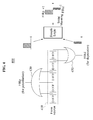
- FIG. 4 is a diagram illustrating an example of a pulse shaper circuit included in a neuromorphic system.
- the neuromorphic system may correspond to the neuromorphic system illustrated in FIG. 1 .
- a pulse shaper circuit may include only a portion of the structures illustrated in FIG. 4 .
- the pulse shaper circuit may form the shape of a neuron spike that is necessary for the STDP operation. That is, the pulse shaper circuit may generate a digital pulse indicating whether pulses corresponding to the spike fired by the neuron circuit are to potentiate or depress the synaptic weight of the synapse circuit.
- the pulse shaper circuit 400 includes a FIR filter 410, a first OR calculator 430, and a second OR calculator 450.
- the FIR filter 410 may be in the form of a 1-bit D flip-flop chain and be configured to store pulses transmitted from the neuron circuit.
- the first OR calculator 430 may generate the digital pulse by performing an OR calculation with respect to at least one pulse corresponding to potentiation of the synaptic weight among the pulses stored in the FIR filter 410.
- the second OR calculator 450 may generate the digital pulse by performing OR calculation with respect to at least one pulse that corresponds to depression of the synaptic weight among the pulses stored in the FIR filter 410.
- Output values of the first OR calculator 430 and the second OR calculator may express the synaptic weights of +1, 0, and -1 through simple calculation.
- the output value '1(+1)' of the first OR calculator 430 may refer to potentiation of the synaptic weight
- the output value '1(-1)' of the second OR calculator 450 may refer to depression of the synaptic weight.
- the output value of the first OR calculator 430 and the second OR calculator 450 is '0,' it may indicate no change to the synaptic network.
- FIG. 5 illustrates an example of a spike-timing dependent plasticity (STDP) operation method of a neuromorphic system.
- the neuromorphic system may correspond to the neuromorphic system illustrated in FIG. 1 .
- a WLx word line that corresponds to an axon of the neuron circuit A 509 is enabled at a falling edge of a pulse shaper signal. Further, pulse values of other neurons may be updated to the synapse circuit through the pulse shaper circuit.
- the IF when IF denotes a signal informing of firing of the neuron has and PS denotes a digital pulse shape generated by the pulse shaper circuit, the IF may have '1' or '0' as a pulse value generated in the pulse generator 330 of FIG. 3 .
- the PS may have a value of 1, -1, or 0. All neurons may each have its IF value and its PS value.
- the foregoing operation may be performed in the STDP logic circuit 507. Whether an update has occurred among a plurality of synapse circuits and updated values of the synapse circuits may be determined based on whether the digital pulses generated in the pulse shaper circuit potentiate or depress the synaptic weight.
- the STDP logic circuit 507 may determine update of the synapse circuits and the updated values, depending on a spike time between digital pulses corresponding to spikes fired by the plurality of neuron circuits.
- the STDP logic circuit 507 may determine an updated value of a synapse circuit that corresponds to a first neuron circuit, based on a second digital pulse value of a second neuron seen from the falling edge of a first digital pulse.
- the STDP logic circuit 507 may determine the updated value as a value for potentiating the synaptic weight. In the event that the second digital pulse precedes the first digital pulse, the STDP logic circuit 507 may determine the updated value as a value for depressing the synaptic weight.
- the STDP logic circuit 507 may determine to maintain the value of the synapse circuit corresponding to the first neuron circuit.
- the value of the second digital pulse of 'other' neuron circuits seen from the falling edge of the first digital pulse corresponding to the spike of the neuron circuit A 509 may occur later than that of the neuron circuit A 509.
- the value '+1' may be obtained when 'other' neuron circuits are seen from the falling edge of the first digital pulse.
- the value '+1' refers to potentiation of the synaptic weight.
- the value of the second digital pulse of 'other' neuron circuits seen from the falling edge of the first neuron corresponding to the spike of the neuron circuit A 509 may be earlier than the neuron circuit A 509, as in Case 2 shown by depression 530.
- the value '-1' may be obtained when 'other' neuron circuits are seen from the falling edge of the first digital pulse.
- the value '-1' refers to depression of the synaptic weight.
- '0' may be obtained as the value of the second digital pulse of 'other' neuron circuits seen from the falling edge of the first neuron corresponding to the spike of the neuron circuit A 509, as illustrated in Case 3 of no change 550.
- neurons corresponding to 505 among the axon lines of the neuron circuit A 509 are not changed at the falling edge of the neuron circuit A 509.
- the neuromorphic system may access the WLx line (refer to the WLx word line of FIG. 1 ) of the synapse circuit corresponding to the first neuron circuit at the falling edge of the first digital pulse corresponding to the fired spike, thereby enabling the WLx line.
- the STDP logic circuit 507 may determine whether an update of the synapse array occurred and the updated value, and access the WLx line (refer to the WLx word line of FIG. 1 ) of the synapse circuit to be updated through an encoder.
- the updated value of the corresponding synapse may be determined by C 1 C 0 output from the STDP logic circuit.
- a high integration and low-power neuromorphic system may be implemented, by flowing only a minor current equivalent to a leakage current to a neuron circuit and a synapse circuit constituting the neuromorphic system.
Landscapes
- Engineering & Computer Science (AREA)
- Physics & Mathematics (AREA)
- Life Sciences & Earth Sciences (AREA)
- Biomedical Technology (AREA)
- Theoretical Computer Science (AREA)
- Health & Medical Sciences (AREA)
- Biophysics (AREA)
- General Health & Medical Sciences (AREA)
- Molecular Biology (AREA)
- Artificial Intelligence (AREA)
- Computational Linguistics (AREA)
- Data Mining & Analysis (AREA)
- Evolutionary Computation (AREA)
- Computing Systems (AREA)
- General Engineering & Computer Science (AREA)
- General Physics & Mathematics (AREA)
- Mathematical Physics (AREA)
- Software Systems (AREA)
- Neurology (AREA)
- Computer Hardware Design (AREA)
- Semiconductor Memories (AREA)
- Static Random-Access Memory (AREA)
Abstract
Description
- The following description relates to a synapse array, a pulse shaper circuit, and a neuromorphic system that includes a synapse array and/or a pulse shaper circuit.
- A physiological brain includes hundreds of billions of neurons that are interconnected with one another in a complicated nerve network. Neurons are considered to be responsible for the intellectual capability for learning and memory. In the cellular level, neurons use their synapses to exchange signals with thousands of other neurons. Thus, the neurons may be considered the structural and functional base units for data transmission. A synapse refers to a junction between two neurons at which an axon of a first neuron and a dendrite of a second neuron are positioned next to each other for transmission of data. A single neuron is generally connected with thousands of other neurons via synapses.
- By manufacturing an artificial nervous system that mimics a biological nervous system in a neuronal level, a data processing method of the brain may be mimicked to achieve a new data processing and storing method.
- A neuromorphic system refers to a semiconductor circuit that is designed to mimic the operation of the biological nervous system. A neuromorphic system may be used in a variety of applications, including in the implementation of an intelligent system that is capable of adapting itself to an unspecified environment.
- In one general aspect, there is provided a synapse array based on a static random access memory (SRAM), the synapse array including a plurality of synapse circuits, in which at least one synapse circuit among the plurality of synapse circuits includes at least one bias transistor and at least two cut-off transistors, and the at least one synapse circuit is configured to charge a membrane node of a neuron circuit connected with the at least one synapse circuit using a sub-threshold leakage current that passed through the at least one bias transistor.
- The at least one synapse circuit may be configured to change a value of the SRAM using a leakage current that passed through the at least two cut-off transistors.
- The neuron circuit may be configured to fire a spike based on a result of comparing a number of occurrences of oscillation pulses generated based on a voltage of the membrane node to a predetermined reference number.
- The neuron circuit may include: a pulse generator configured to generate an oscillation pulse based on a voltage of the membrane node; a counter configured to count a number of occurrences of the oscillation pulse; and a comparator configured to compare the number of occurrences to a predetermined reference number.
- The comparator may be configured to compare the reference number with the number of occurrences, in synchronization with a clock signal periodically input.
- The neuron circuit may further include a transistor connected to a ground. The oscillation pulse may be used to reset the membrane node by activating the transistor.
- The at least two cut-off transistors may include a first cut-off transistor and a second cut-off transistor. The first cut-off transistor may be connected to a power voltage for pull-up. The second cut-off transistor may be connected to a ground for pull-down. The at least one bias transistor may be connected to the membrane node of the neuron circuit connected with the at least one synapse circuit.
- In another general aspect, there is provided a pulse shaper circuit that is configured to generate a digital pulse indicating whether pulses corresponding to spikes fired by a neuron circuit potentiate or depress a synaptic weight of a synapse circuit.
- The general aspect of the pulse shaper circuit may further include: a finite impulse response (FIR) filter comprising a 1-bit D flip flop chain configured to store the pulses; a first OR calculator configured to generate the digital pulse by performing OR calculation with respect to at least one pulse corresponding to potentiation of the synaptic weight among the stored pulses; and a second OR calculator is configured to generate the digital pulse by performing OR calculation with respect to at least one pulse corresponding to depression of the synaptic weight among the stored pulses.
- The pulse shaper circuit may be configured to generate the digital pulse for maintaining the synaptic weight based on a value of the first OR calculator and a value of the second OR calculator.
- In another general aspect, there is provided a neuromorphic system including: a synapse array based on a SRAM, the synapse array including at least one synapse circuit; a neuron circuit connected with the synapse circuit, the synapse circuit being configured to charge a membrane node of the neuron circuit using a sub-threshold leakage current that passed through at least one bias transistor of the synapse array, and the neuron circuit being configured to fire spikes based on a voltage of the membrane node; and a pulse shaper circuit configured to generate a digital pulse corresponding to the fired spikes.
- The synapse array may include a plurality of synapse circuits, the plurality of synapse circuits including the at least one synapse circuit. The neuromorphic system may include a plurality of neuron circuits and a plurality of pulse shaper circuits. The neuromorphic system may further include a spike-timing dependent plasticity (STDP) logic circuit configured to determine an update state of a synapse circuit among the plurality of synapse circuits and an updated value for the synapse circuit based on the digital pulse, and an encoder configured to access a synapse circuit to be updated according to the digital pulse.
- The neuron circuit may be configured to fire spikes based on a result of comparing a number of occurrences of oscillation pulses generated based on the voltage of the membrane node to a predetermined reference number.
- The synapse array may further include at least two cut-off transistors, and may be configured to change a value of the SRAM using a leakage current that passed through the at least two cut-off transistors.
- The neuron circuit may include: a pulse generation unit configured to generate an oscillation pulse based on a voltage of the membrane node; a counter configured to count a number of occurrences of the oscillation pulse; and a comparator configured to compare the number of occurrences to a predetermined reference number.
- The neuron circuit may further include a transistor connected to a ground. The oscillation pulse may be used to reset the membrane node by activating the transistor.
- The at least two cut-off transistors may include a first cut-off transistor and a second cut-off transistor. The first cut-off transistor may be connected to a power voltage for pull-up. The second cut-off transistor may be connected to a ground for pull-down. The at least one bias transistor may be connected to the membrane node of the neuron circuit connected with the synapse circuit.
- The pulse shaper circuits may be configured to generate a digital pulse indicating whether pulses corresponding to spikes fired by a neuron circuit potentiate or depress a synaptic weight of the synapse circuit.
- The STDP logic circuit may be configured to determine an update state of the plurality of synapse circuits and an updated value for the synapse circuits based on whether the digital pulse potentiates or depresses the synaptic weight.
- The STDP logic circuit may be configured to determine the update state and the updated value of the synapse circuits, depending on a spike time between digital pulses corresponding to the spikes fired by the plurality of neuron circuits.
- The neuromorphic system may be configured to enable a write line (WL) of a synapse circuit corresponding to a first neuron circuit at a falling edge of a first digital pulse corresponding to a spike fired by the first neuron circuit in response to the first neuron circuit among the plurality of neuron circuits firing the spike.
- The STDP logic circuit may be configured to determine the updated value of the synapse circuit corresponding to the first neuron circuit based on a value of a second digital pulse of a second neuron seen from the falling edge of the first digital pulse.
- The STDP logic circuit may be configured to update a value for potentiating the synaptic weight as the updated value in response to the first digital pulse preceding the second digital pulse.
- The STDP logic circuit may be configured to update a value for depressing the synaptic weight as the updated value in response to the second digital pulse preceding the first digital pulse.
- The STDP logic circuit may be configured to determine to maintain the value of the synapse circuit corresponding to the first neuron circuit in response to '0' being detected at the falling edge of the first digital pulse.
- The encoder may be configured to transmit the updated value to the synapse circuits according to the digital pulse.
- Other features and aspects will be apparent from the following detailed description, the drawings, and the claims.
-
FIG. 1 is a diagram illustrating an overall structure of an example of a neuromorphic system. -
FIG. 2 is a diagram illustrating an example of a synapse circuit included in a neuromorphic system. -
FIG. 3 is a diagram illustrating an example of a neuron circuit included in a neuromorphic system. -
FIG. 4 is a diagram illustrating an example of a pulse shaper circuit included in a neuromorphic system. -
FIG. 5 is a diagram illustrating an example of a spike-timing dependent plasticity (STDP) operation method of a neuromorphic system. - Throughout the drawings and the detailed description, unless otherwise described or provided, the same drawing reference numerals will be understood to refer to the same elements, features, and structures. The drawings may not be to scale, and the relative size, proportions, and depiction of elements in the drawings may be exaggerated for clarity, illustration, and convenience.
- The following detailed description is provided to assist the reader in gaining a comprehensive understanding of the methods, apparatuses, and/or systems described herein. However, various changes, modifications, and equivalents of the systems, apparatuses, and/or methods described herein will be apparent to one of ordinary skill in the art. The progression of processing steps and/or operations described is an example; however, the sequence of steps and/or operations is not limited to that set forth herein and may be changed as is known in the art, with the exception of steps and/or operations necessarily occurring in a certain order. Also, description of well-known functions and constructions may be omitted for increased clarity and conciseness.
- The features described herein may be embodied in different forms, and are not to be construed as being limited to the examples described herein. Rather, the examples described herein have been provided so that this disclosure will be thorough and complete, and will convey the full scope of the disclosure to one of ordinary skill in the art.
-
FIG. 1 illustrates an overall structure of an example of aneuromorphic system 100. - Referring to
FIG. 1 , theneuromorphic system 100 includes a static random access memory (SRAM)-basedsynapse array 110, a plurality ofneuron circuits 130, a plurality ofpulse shaper circuits 150, a spike-timing dependent plasticity (STDP)logic circuit 170, and anencoder 190. However, in other examples, a neuromorphic system may include one or more of the SRAM-based synapse array, neurons circuits, pulse shaper circuits, STDP logic circuit and encoder, without including all of these structures. - Referring to
FIG. 1 , the SRAM-basedsynapse array 110 includes a plurality of synapse circuits based on an SRAM structure. Each of the synapse circuits may include at least one bias transistor and at least two cut-off transistors. - The synapse circuit may charge membrane nodes of the
neuron circuits 130 that is connected with the synapse circuit, using a sub-threshold leakage current that passed through the at least one bias transistor. In addition, the synapse circuit may change a value of the SRAM by using a leakage current that passes through the at least two cut-off transistors. - The synapse circuit may include the at least two cut-off transistors, for example, a first cut-off transistor and a second cut-off transistor. The first cut-off transistor may be connected to a voltage drain drain (VDD) for pull-up. The second cut-off transistor may be connected to a ground (GND) for pull-down. The at least one bias transistor may be connected to the membrane nodes of the
neuron circuits 130 that is connected to the synapse circuit. - WLx/WLxB indicated at the
synapse array 110 refers to a word line, that is, a line for selecting an address of an axon. In WLx/WLxB, x refers to an order of each line. In this example, x may be a natural number ranging from 0 to 3. A logic value of WLx of thesynapse array 110 is 1. When a corresponding line is selected, an STDP result may be used for the SRAM through C1C0x, that is, STDP information of each neuron transmitted through an STDP logic circuit. STDP refers to a learning mechanism postulated to exist in synapses of biological nerve networks. Based on STDP, synaptic efficacy or weight is slightly altered between two neurons based on information such as the timing of a pre-synaptic spike in a pre-synaptic neuron and a post-synaptic spike in a post-synaptic neuron. That is, a synaptic circuit may be potentiated or depressed to change the efficacy of data transmission between two neurons. The operation and configuration of an example of the synapse circuit are further described below with reference toFIG. 2 . - The plurality of
neuron circuits 130 may fire spikes based on a result of comparing a number of occurrences of oscillation pulses generated on the basis of an input voltage input from the membrane nodes, to a predetermined reference number. An example of theneuron circuit 130 is further described below with reference toFIG. 3 . - The plurality of
pulse shaper circuits 150 may receive a signal transmitted from theneuron circuit 130, and may generate a pulse for the STDP operation based on the signal. Thepulse shaper circuits 150 may generate digital pulses corresponding to the spikes fired at theneuron circuits 130. Thepulse shaper circuits 150 may generate the digital pulses that indicate whether pulses corresponding to the fired spikes potentiate (strengthen) or depress (weaken) a synaptic weight of the synapse circuit. An example of thepulse shaper circuit 150 is further described below with reference toFIG. 4 . - The
STDP logic circuit 170 may receive the signal generated by thepulse shaper circuits 150, and may perform the STDP operation based on the signal. That is, theSTDP logic circuit 170 may determine an update state of the plurality of synapse circuits and updated values for the synapse circuits, based on the digital pulses generated by thepulse shaper circuits 150. In addition, theSTDP logic circuit 170 may include an address event representation (AER) function, by which theSTDP logic circuit 170 may transmit a test result related to theneuron circuits 130 and information regarding firing generated in arandom neuron circuit 130 toother neuron circuits 130. The updated value determined by theSTDP logic circuit 170 may be transmitted to thesynapse array 110 through the WBLx line. - The
STDP logic circuit 170 may determine the presence of absence of an updating event (update state) and the updated values of the synapse circuits, based on a spike time between the digital pulses corresponding to the spikes fired by the plurality ofneuron circuits 130. - The operation of the
STDP logic circuit 170 is further described below with reference toFIG. 5 . - The
encoder 190 may access thesynapse array 110 according to the digital pulses generated by thepulse shapers 150. Theencoder 190 may access the synapse arrays to be updated according to the digital pulses, or transmit the updated values to the synapse circuits according to the digital pulses. For example, in the event that a firing occurred in aneuron circuit 130, the pulse generated at apulse shaper circuit 150, for example '1', may be transmitted to theencoder 190. In response, theencoder 190 may transmit a logic value '1' to WLO to update the synaptic weight of the synapse circuit corresponding to theneuron circuit 130. In this example, the WLO line (or other WLx line) refers to a line for selecting the address of a word line. That is, the WLO line (or other WLx line) may correspond to a Write Enable state. In the event that WLO is equal to '1', states of the synapse circuits corresponding to a first word line, for example, corresponding to an axon of neuron circuit A inFIG. 5 may be the Write Enable state. However, in the event that theneuron circuit 130 did not fire, theencoder 190 does not transmit the pulse and, in this state, the logic value '0' may be applied to WL2. Therefore, synapse circuits corresponding to a third word line may be in a Write Disable state and data may not be written. - For example, in the event that a first neuron circuit among the plurality of
neuron circuits 130 fired the spike, the neuromorphic system may enable a write line, for example the WLX line, of the synapse circuit corresponding to the first neuron circuit in a falling edge of a first digital pulse corresponding to the fired spike. - Generally, the neuromorphic system may be greatly affected by a leakage current of devices, a mismatch between devices, and a process voltage temperature (PVT) variation. Further, with an increase in the number of neuron circuits and synapse circuits included in a neuromorphic system, more scale-down complementary metal oxide semiconductor (CMOS) process may be used for high integration. However, as the process becomes more scale-down, the leakage current from semiconductor components may further increase. The increase in leakage current may potentially cause continuous firings inside a neuron circuit even when no external stimulation is applied to the neuron circuit.
- In general, leakage current has been considered an adverse side effect in designing a neuromorphic system. However, according to one example, the neuromorphic system may be implemented in such a way that it meets the demand for high integration and low power, by using a small amount of current equivalent to the amount of leakage current.
-
FIG. 2 illustrates an example of asynapse circuit 200 included in a neuromorphic system. The neuromorphic system may correspond to the neuromorphic system illustrated inFIG. 1 . Further, according to another example, a synapse circuit may include only a portion of the structures illustrated inFIG. 2 . - Referring to
FIG. 2 , thesynapse circuit 200 includes at least two cut-offtransistors bias transistor 260. - The
synapse circuit 200 is configured to charge a membrane node of a neuron circuit connected with thesynapse circuit 200, using a sub-threshold leakage current that passed through the at least onebias transistor 260. - The at least two cut-off
transistors transistor 210 and a second cut-offtransistor 230. - In this example, the first cut-off
transistor 210 is a P-metal oxide semiconductor (P-MOS) transistor. The first cut-offtransistor 210 is connected to a power voltage VDD for pull-up. The second cut-offtransistor 230 is an N-MOS transistor and is connected to a ground GND for pull-down. - The
bias transistor 260 is a transistor located at a last position of athird device 250 in which three P-MOS transistors are serially connected. Thebias transistor 260 may be connected to the membrane node of the neuron circuit connected to thesynapse circuit 200. Thethird device 250 in which the three P-MOS transistors are serially connected may be connected to an RWLBx line and a Cmemx line. Thethird device 250 may be used in performing a read operation. In the event that firing occurs at a neuron circuit corresponding to the RWLBx line, all neuron circuits that are connected to the neuron circuit may have a logic value '1.' - While a write line WLx of the
synapse circuit 200 is enabled, in this example, thesynapse circuit 200 may change a value of thecross-coupled inverter 240 to a value provided by awriting circuit 220. At most time, the write line WLx is in a disabled state. - A neuromorphic system using a general SRAM structure may be implemented only with a
cross-coupled inverter 240 configuration. In such a case, because a leakage current between the power voltage VDD and the ground GND, flowing through thecross-coupled inverter 240, may be great in amount, the leakage power consumption may increase. - However, the neuromorphic system according to the present disclosure may considerably reduce the leakage power consumption caused by the first cut-off
transistor 210 and the second cut-offtransistor 230. For example, when the first cut-offtransistor 210 and the second cut-offtransistor 230 are in an off state, the leakage current between the power voltage VDD and the ground GND may be substantially suppressed, thereby reducing the leakage power consumption. - In the event that a value of a node n1 is '0' in the
cross-coupled inverter 240, the SRAM may have a value of approximately '0.' In the event that the value of the node n1 is '1,' the SRAM may have a value that is approximately '1' and a value of a node n2 may be approximately '0.' Therefore, the node n2 may allow the current that is necessary for operation to flow toward the membrane node. Here, a voltage slightly lower than the power voltage VDD may be applied to thebias transistor 260 located at the third position of thethird device 250 through an external bias circuit. Accordingly, only a minor amount of current equivalent to the sub-threshold leakage current may flow inside thebias transistor 260. - In the event that firing occurs at the neuron circuit during a writing operation, it is possible for the current to flow among the neuron circuits in different directions according to whether the synaptic weight of the synapse circuit corresponds to potentiation or depression.
- In the event that the synaptic weight is '1,' the current may flow from a pre-synaptic neuron circuit to a post-synaptic neuron circuit. Conversely, in the event that the synaptic weight is '-1,' the current may flow from a post-synaptic neuron circuit to a pre-synaptic neuron circuit.
- In addition, a first device, that is, the
writing circuit 220 including two serially connected N-MOS transistors and two serially connected P-MOS transistors may be connected to the WLx word line as a result of the STDP and therefore may perform the writing operation. - Referring back to the synapse circuit of
FIG. 2 , in the event that the transistor is turned on, a current of several nano amperes (1x10⁻⁹A) may flow through the transistor. In the event that the transistor is in an OFF state, a current of several pico amperes (1x10-12 A) may flow through the transistor. The magnitudes of currents may be considered as a leakage current level of a general synapse circuit. According to one example, it is possible to operate the neuron circuit with such a small amount of current, thereby achieving a high level of integration and a reduction of power consumption in the neuromorphic system. - Because the synapse circuit according to the embodiment uses a synapse circuit based on the SRAM structure, the synapse circuit takes up a relatively smal area and is efficient in achieving high integration. Moreover, the synapse circuit may charge the membrane node of the neuron with a small amount of current using the cut-off transistors. Therefore, even with a highly integrated circuit, a firing rate of the neuron circuit may be maintained at a level similar to an actual biological neuron.
- Furthermore, due to the cut-off transistors that is connected to the power voltage VDD and the ground GND through pull-up and pull-down, a leakage current may not be generated even in a static state remembering the synaptic weight. Therefore, a neuromorphic system that operates with low power consumption may be achieved.
-
FIG. 3 illustrates an example of aneuron circuit 300 included in a neuromorphic system. The neuromorphic system may correspond to the neuromorphic system illustrated inFIG. 1 . Further, according to another example, a neuron circuit may include only a portion of the structures illustrated inFIG. 3 . - Referring to
FIG. 3 , theneuron circuit 300 according to one example includes apulse generator 310, acounter 330, and acomparator 350. - In the event that a voltage is applied through a membrane node, the
pulse generator 310 may generate an oscillation pulse based on the voltage. For example, the voltage applied to thepulse generator 310 may have a wave form similar to awave form 301 illustrated inFIG. 3 . The oscillation pulse generated by thepulse generator 310 may be a digital pulse similar to awave form 303 illustrated inFIG. 3 . - The
pulse generator 310 includes atransistor 320. Thetransistor 320 connects to a ground GND through a source terminal thereof, and connects to the membrane node through a drain terminal thereof. The oscillation pulse generated by thepulse generator 310 may activate thetransistor 320, thereby resetting the membrane node. By resetting the membrane node, thetransistor 320 may participate in the generation of the oscillation pulse. - The
counter 330 may count a number of occurrences of the oscillation pulses or a number of the oscillation pulses generated in thepulse generator 350. - The
comparator 350 may compare a predetermined reference number with the number of occurrences of the oscillation pulses counted by thecounter 330. Thecomparator 350 may compare the reference number with the number of occurrences, in synchronization with a clock signal that is periodically input. - The
comparator 350 may fire a spike based on a result of the comparison. The pulse generated in thecomparator 350 may be connected to a reset terminal of thecounter 330 and be transmitted to a pulse shaper circuit. Here, the transmitted pulse may pass through a finite impulse response (FIR) filter and be overwritten to a synaptic weight of the synapse circuit by an STDP logic circuit. -
FIG. 4 is a diagram illustrating an example of a pulse shaper circuit included in a neuromorphic system. The neuromorphic system may correspond to the neuromorphic system illustrated inFIG. 1 . Further, according to another example, a pulse shaper circuit may include only a portion of the structures illustrated inFIG. 4 . - Referring to
FIG. 4 , the pulse shaper circuit according to one example may form the shape of a neuron spike that is necessary for the STDP operation. That is, the pulse shaper circuit may generate a digital pulse indicating whether pulses corresponding to the spike fired by the neuron circuit are to potentiate or depress the synaptic weight of the synapse circuit. - The
pulse shaper circuit 400 includes aFIR filter 410, a first ORcalculator 430, and a second ORcalculator 450. - The
FIR filter 410 may be in the form of a 1-bit D flip-flop chain and be configured to store pulses transmitted from the neuron circuit. - The first OR
calculator 430 may generate the digital pulse by performing an OR calculation with respect to at least one pulse corresponding to potentiation of the synaptic weight among the pulses stored in theFIR filter 410. - The second OR
calculator 450 may generate the digital pulse by performing OR calculation with respect to at least one pulse that corresponds to depression of the synaptic weight among the pulses stored in theFIR filter 410. - Output values of the first OR
calculator 430 and the second OR calculator may express the synaptic weights of +1, 0, and -1 through simple calculation. For example, the output value '1(+1)' of the first ORcalculator 430 may refer to potentiation of the synaptic weight, and the output value '1(-1)' of the second ORcalculator 450 may refer to depression of the synaptic weight. Further, in the event that the output value of the first ORcalculator 430 and the second ORcalculator 450 is '0,' it may indicate no change to the synaptic network. -
FIG. 5 illustrates an example of a spike-timing dependent plasticity (STDP) operation method of a neuromorphic system. The neuromorphic system may correspond to the neuromorphic system illustrated inFIG. 1 . - Referring to
FIG. 5 , the STDP operation of the neuromorphic system is described. - Presuming that a firing has occurred in a
neuron circuit A 509 among a plurality of neuron circuits, a WLx word line that corresponds to an axon of theneuron circuit A 509 is enabled at a falling edge of a pulse shaper signal. Further, pulse values of other neurons may be updated to the synapse circuit through the pulse shaper circuit. - For example, when IF denotes a signal informing of firing of the neuron has and PS denotes a digital pulse shape generated by the pulse shaper circuit, the IF may have '1' or '0' as a pulse value generated in the
pulse generator 330 ofFIG. 3 . The PS may have a value of 1, -1, or 0. All neurons may each have its IF value and its PS value. - Presuming that a firing has occurred in the
neuron circuit A 509, simple logic calculation may be performed with respect to the PS values of other neurons and the IF value of theneuron circuit A 509 when the falling edge of the pulse shaper signal starts. Based on a result of the logic calculation, the synapse circuit may be updated. - The foregoing operation may be performed in the STDP logic circuit 507. Whether an update has occurred among a plurality of synapse circuits and updated values of the synapse circuits may be determined based on whether the digital pulses generated in the pulse shaper circuit potentiate or depress the synaptic weight.
- In addition, the STDP logic circuit 507 may determine update of the synapse circuits and the updated values, depending on a spike time between digital pulses corresponding to spikes fired by the plurality of neuron circuits.
- The STDP logic circuit 507 may determine an updated value of a synapse circuit that corresponds to a first neuron circuit, based on a second digital pulse value of a second neuron seen from the falling edge of a first digital pulse.
- In the event that the first digital pulse precedes the second digital pulse, the STDP logic circuit 507 may determine the updated value as a value for potentiating the synaptic weight. In the event that the second digital pulse precedes the first digital pulse, the STDP logic circuit 507 may determine the updated value as a value for depressing the synaptic weight.
- In the event that a value '0' is detected at the falling edge of the first digital pulse, the STDP logic circuit 507 may determine to maintain the value of the synapse circuit corresponding to the first neuron circuit.
- Hereinafter, relationships between the
neuron circuit A 509 and 'other' neuron circuits is further described to explain the operation of the STDP logic circuit 507 based on an order between the first digital pulse and the second digital pulse. - For example, presuming that a firing has occurred in the
neuron circuit A 509 ofFIG. 5 , the value of the second digital pulse of 'other' neuron circuits seen from the falling edge of the first digital pulse corresponding to the spike of theneuron circuit A 509 may occur later than that of theneuron circuit A 509. InCase 1 illustrated inFIG. 5 , in the case ofpotentiation 510, the value '+1' may be obtained when 'other' neuron circuits are seen from the falling edge of the first digital pulse. The value '+1' refers to potentiation of the synaptic weight. The STDP logic circuit 507 may generate a pulse (C1C0 = 00) for potentiation update of the synaptic weight. In this example, neurons corresponding to 501 among axon lines of the neuron circuit A may be updated to a pulse value '+1' of 'other' neuron circuits. That is, C1C0 = 00, at the falling edge of theneuron circuit A 509. - The value of the second digital pulse of 'other' neuron circuits seen from the falling edge of the first neuron corresponding to the spike of the
neuron circuit A 509 may be earlier than theneuron circuit A 509, as inCase 2 shown bydepression 530. InCase 2 illustrated inFIG. 5 , the value '-1' may be obtained when 'other' neuron circuits are seen from the falling edge of the first digital pulse. The value '-1' refers to depression of the synaptic weight. The STDP logic circuit 507 may generate a pulse (C1C0= 11) for depression update of the synaptic weight. In this example, neurons corresponding to 503 among the axon lines of theneuron circuit A 509 may be updated to a pulse value '-1' of 'other' neuron circuits. That is, C1C0 = 11, at the falling edge of theneuron circuit A 509. - In addition, '0' may be obtained as the value of the second digital pulse of 'other' neuron circuits seen from the falling edge of the first neuron corresponding to the spike of the
neuron circuit A 509, as illustrated inCase 3 of nochange 550. In this case, a time difference between the first digital pulse and the second digital pulse is so great that the synaptic weight is not influenced at all. That is, in this case, a previous value of the synaptic weight may be maintained. Therefore, since the STDP logic circuit 507 needs to not update the synaptic weight, the value is controlled to meet C1C0 = 01 so that the transistors are in its OFF state. Accordingly, an SRAM value is not changed. Here, neurons corresponding to 505 among the axon lines of theneuron circuit A 509 are not changed at the falling edge of theneuron circuit A 509. - When a spike is fired at the first neuron circuit among the plurality of neuron circuits, the neuromorphic system may access the WLx line (refer to the WLx word line of
FIG. 1 ) of the synapse circuit corresponding to the first neuron circuit at the falling edge of the first digital pulse corresponding to the fired spike, thereby enabling the WLx line. - As described above, the STDP logic circuit 507 may determine whether an update of the synapse array occurred and the updated value, and access the WLx line (refer to the WLx word line of
FIG. 1 ) of the synapse circuit to be updated through an encoder. Here, the updated value of the corresponding synapse may be determined by C1C0 output from the STDP logic circuit. - With the various examples described above, a high integration and low-power neuromorphic system may be implemented, by flowing only a minor current equivalent to a leakage current to a neuron circuit and a synapse circuit constituting the neuromorphic system.
- While this disclosure includes specific examples, it will be apparent to one of ordinary skill in the art that various changes in form and details may be made in these examples without departing from the scope of the claims and their equivalents. The examples described herein are to be considered in a descriptive sense only, and not for purposes of limitation. Descriptions of features or aspects in each example are to be considered as being applicable to similar features or aspects in other examples. Suitable results may be achieved if the described techniques are performed in a different order, and/or if components in a described system, architecture, device, or circuit are combined in a different manner and/or replaced or supplemented by other components or their equivalents. Therefore, the scope of the disclosure is defined not by the detailed description, but by the claims and their equivalents, and all variations within the scope of the claims and their equivalents are to be construed as being included in the disclosure.
Claims (15)
- A synapse array based on a static random access memory (SRAM), the synapse array comprising a plurality of synapse circuits,
wherein at least one synapse circuit among the plurality of synapse circuits comprises at least one bias transistor and at least two cut-off transistors, and the at least one synapse circuit is configured to charge a membrane node of a neuron circuit connected with the at least one synapse circuit using a sub-threshold leakage current that passed through the at least one bias transistor. - The synapse array of claim 1, wherein the at least one synapse circuit is configured to change a value of the SRAM using a leakage current that passed through the at least two cut-off transistors.
- The synapse array of claim 1 or 2, wherein the neuron circuit is configured to fire a spike based on a result of comparing a number of occurrences of oscillation pulses generated based on a voltage of the membrane node to a predetermined reference number.
- The synapse array of any of the previous claims, wherein the neuron circuit comprises:a pulse generator configured to generate an oscillation pulse based on a voltage of the membrane node;a counter configured to count a number of occurrences of the oscillation pulse; anda comparator configured to compare the number of occurrences to a predetermined reference number;wherein the comparator is preferably configured to compare the reference number with the number of occurrences, in synchronization with a clock signal periodically input; and/orwherein, preferably,the neuron circuit further comprises a transistor connected to a ground, andthe oscillation pulse is used to reset the membrane node by activating the transistor.
- The synapse array of any of the previous claims, wherein
the at least two cut-off transistors comprise a first cut-off transistor and a second cut-off transistor,
the first cut-off transistor is connected to a power voltage for pull-up,
the second cut-off transistor is connected to a ground for pull-down, and
the at least one bias transistor is connected to the membrane node of the neuron circuit connected with the at least one synapse circuit. - A neuromorphic system comprising:a synapse array as defined in any of the previous claims;a neuron circuit having a membrane node, the neuron circuit being connected with said at least one synapse circuit of the synapse array, the at least one synapse circuit being configured to charge the membrane node of the neuron circuit, and the neuron circuit being configured to fire spikes based on a voltage of the membrane node; anda pulse shaper circuit configured to generate a digital pulse corresponding to the fired spikes.
- The neuromorphic system of claim 6, wherein the neuromorphic system comprises a plurality of neuron circuits and a plurality of pulse shaper circuits; and
the neuromorphic system further comprises a spike-timing dependent plasticity (STDP) logic circuit configured to determine an update state of a synapse circuit among the plurality of synapse circuits and an updated value for the synapse circuit based on a digital pulse; and
an encoder configured to access a synapse circuit to be updated according to the digital pulse. - The neuromorphic system of claim 7, wherein the plurality of pulse shaper circuits are configured to generate a digital pulse indicating whether pulses corresponding to spikes fired by a neuron circuit potentiate or depress a synaptic weight of the synapse circuit.
- The neuromorphic system of claim 8, wherein the STDP logic circuit is configured to determine an update state of the plurality of synapse circuits and an updated value for the synapse circuits based on whether the digital pulse potentiates or depresses the synaptic weight.
- The neuromorphic system of claim 9, wherein the STDP logic circuit is configured to determine the update states and the updated values of the synapse circuits, depending on a spike time between digital pulses corresponding to the spikes fired by the plurality of neuron circuits.
- The neuromorphic system of claim 10, wherein the neuromorphic system is configured to enable a write line (WL) of a synapse circuit corresponding to a first neuron circuit at a falling edge of a first digital pulse corresponding to a spike fired by the first neuron circuit in response to the first neuron circuit among the plurality of neuron circuits firing the spike.
- The neuromorphic system of claim 11, wherein the STDP logic circuit is configured to determine the updated value of the synapse circuit corresponding to the first neuron circuit based on a value of a second digital pulse of a second neuron seen from the falling edge of the first digital pulse;
wherein the STDP logic circuit is preferably configured to update a value for potentiating the synaptic weight as the updated value in response to the first digital pulse preceding the second digital pulse; and/or
wherein the STDP logic circuit is preferably configured to update a value for depressing the synaptic weight as the updated value in response to the second digital pulse preceding the first digital pulse; and/or
wherein the STDP logic circuit is preferably configured to determine to maintain the value of the synapse circuit corresponding to the first neuron circuit in response to '0' being detected at the falling edge of the first digital pulse. - The neuromorphic system of any of the claims 7-12, wherein the encoder is configured to transmit the updated value to the synapse circuits according to the digital pulse.
- A pulse shaper circuit configured to generate a digital pulse indicating whether pulses corresponding to spikes fired by a neuron circuit potentiate or depress a synaptic weight of a synapse circuit.
- The pulse shaper circuit of claim 14, comprising:a finite impulse response (FIR) filter comprising a 1-bit D flip flop chain configured to store the pulses;a first OR calculator configured to generate the digital pulse by performing OR calculation with respect to at least one pulse corresponding to potentiation of the synaptic weight among the stored pulses; anda second OR calculator is configured to generate the digital pulse by performing OR calculation with respect to at least one pulse corresponding to depression of the synaptic weight among the stored pulses;wherein the pulse shaper circuit is preferably configured to generate the digital pulse for maintaining the synaptic weight based on a value of the first OR calculator and a value of the second OR calculator.
Applications Claiming Priority (2)
| Application Number | Priority Date | Filing Date | Title |
|---|---|---|---|
| KR20130065669 | 2013-06-10 | ||
| KR1020140016336A KR102382172B1 (en) | 2013-06-10 | 2014-02-13 | Synapse array, pulse shaper circuit and neuromorphic system including the synapse array and the pulse shaper circuit |
Publications (3)
| Publication Number | Publication Date |
|---|---|
| EP2814036A2 true EP2814036A2 (en) | 2014-12-17 |
| EP2814036A3 EP2814036A3 (en) | 2015-04-01 |
| EP2814036B1 EP2814036B1 (en) | 2020-07-08 |
Family
ID=50771443
Family Applications (1)
| Application Number | Title | Priority Date | Filing Date |
|---|---|---|---|
| EP14169845.6A Active EP2814036B1 (en) | 2013-06-10 | 2014-05-26 | Synapse array, pulse shaper circuit and neuromorphic system |
Country Status (2)
| Country | Link |
|---|---|
| EP (1) | EP2814036B1 (en) |
| CN (1) | CN104240753B (en) |
Cited By (6)
| Publication number | Priority date | Publication date | Assignee | Title |
|---|---|---|---|---|
| CN109844772A (en) * | 2016-11-09 | 2019-06-04 | 国际商业机器公司 | Memory unit |
| US10459724B2 (en) | 2016-01-18 | 2019-10-29 | Huawei Technologies Co., Ltd. | Memory device, and data processing method based on multi-layer RRAM crossbar array |
| CN111756352A (en) * | 2020-05-18 | 2020-10-09 | 北京大学 | Pulse array time domain filtering method, device, equipment and storage medium |
| US11379714B2 (en) | 2018-05-29 | 2022-07-05 | British Cayman Islands Intelligo Technology Inc. | Architecture of in-memory computing memory device for use in artificial neuron |
| US11636883B2 (en) | 2016-03-18 | 2023-04-25 | Semiconductor Energy Laboratory Co., Ltd. | Semiconductor device and system using the same |
| US11893474B2 (en) | 2015-10-23 | 2024-02-06 | Semiconductor Energy Laboratory Co., Ltd. | Semiconductor device and electronic device |
Families Citing this family (11)
| Publication number | Priority date | Publication date | Assignee | Title |
|---|---|---|---|---|
| US10586147B2 (en) * | 2016-09-22 | 2020-03-10 | Intel Corporation | Neuromorphic computing device, memory device, system, and method to maintain a spike history for neurons in a neuromorphic computing environment |
| CN110036443B (en) * | 2016-11-30 | 2023-08-08 | 国立研究开发法人科学技术振兴机构 | Neuron circuit, signal transmission system, and switching circuit |
| US10248906B2 (en) * | 2016-12-28 | 2019-04-02 | Intel Corporation | Neuromorphic circuits for storing and generating connectivity information |
| KR20180133061A (en) | 2017-06-05 | 2018-12-13 | 에스케이하이닉스 주식회사 | Synapse Array of Neuromorphic Device Including Synapses Having Ferro-electric Field Effect Transistors and Operation Method of the Same |
| CN107578096A (en) * | 2017-09-21 | 2018-01-12 | 胡明建 | A kind of voltage-frequency formula selects the design method of end artificial neuron |
| CN109829539A (en) * | 2017-11-23 | 2019-05-31 | 旺宏电子股份有限公司 | Class nerve computing device |
| WO2019147522A2 (en) * | 2018-01-23 | 2019-08-01 | Anaflash Inc. | Neural network circuits having non-volatile synapse arrays |
| US11586882B2 (en) * | 2018-01-24 | 2023-02-21 | International Business Machines Corporation | Synapse memory |
| FR3081073B1 (en) * | 2018-05-14 | 2021-10-08 | Univ Lille | COMMUTED ARTIFICIAL SYNAPSE |
| CN109858619A (en) * | 2019-01-22 | 2019-06-07 | 杭州电子科技大学 | Circuit occurs for the nerve impulse based on spin oscillator |
| CN111325330B (en) * | 2020-02-19 | 2022-10-11 | 北京大学 | Synaptic symmetry time-dependent plasticity algorithm circuit and array structure thereof |
Family Cites Families (11)
| Publication number | Priority date | Publication date | Assignee | Title |
|---|---|---|---|---|
| ATE429085T1 (en) * | 2000-08-24 | 2009-05-15 | Continental Automotive Gmbh | RECEPTION SYSTEM WITH ANTENNA DIVERSITY |
| GB0203605D0 (en) * | 2002-02-15 | 2002-04-03 | Wood John | Hierarchical clocking system |
| TWI316787B (en) * | 2005-04-13 | 2009-11-01 | Via Tech Inc | Method for optimizing critical path timing in a logic synthesis flow and data processing system |
| US7292069B2 (en) * | 2005-12-30 | 2007-11-06 | Intel Corporation | Locally asynchronous, block-level synchronous, configurable logic blocks with sub-threshold analog circuits |
| CN101997538B (en) * | 2009-08-19 | 2013-06-05 | 中国科学院半导体研究所 | Pulse coupling based silicon-nanowire complementary metal oxide semiconductors (CMOS) neuronal circuit |
| US9092736B2 (en) * | 2010-07-07 | 2015-07-28 | Qualcomm Incorporated | Communication and synapse training method and hardware for biologically inspired networks |
| US8473439B2 (en) * | 2010-12-08 | 2013-06-25 | International Business Machines Corporation | Integrate and fire electronic neurons |
| US8856055B2 (en) * | 2011-04-08 | 2014-10-07 | International Business Machines Corporation | Reconfigurable and customizable general-purpose circuits for neural networks |
| KR101888468B1 (en) * | 2011-06-08 | 2018-08-16 | 삼성전자주식회사 | Synapse for a function cell of spike-timing-dependent plasticity(stdp), the function cell of spike-timing-dependent plasticity, and a neuromorphic circuit using the function cell of spike-timing-dependent plasticity |
| CN102496385B (en) * | 2011-12-26 | 2014-04-16 | 电子科技大学 | Spike timing activity conversion circuit |
| CN102610274B (en) * | 2012-04-06 | 2014-10-15 | 电子科技大学 | Weight adjustment circuit for variable-resistance synapses |
-
2014
- 2014-05-04 CN CN201410185178.8A patent/CN104240753B/en active Active
- 2014-05-26 EP EP14169845.6A patent/EP2814036B1/en active Active
Non-Patent Citations (1)
| Title |
|---|
| None |
Cited By (6)
| Publication number | Priority date | Publication date | Assignee | Title |
|---|---|---|---|---|
| US11893474B2 (en) | 2015-10-23 | 2024-02-06 | Semiconductor Energy Laboratory Co., Ltd. | Semiconductor device and electronic device |
| US10459724B2 (en) | 2016-01-18 | 2019-10-29 | Huawei Technologies Co., Ltd. | Memory device, and data processing method based on multi-layer RRAM crossbar array |
| US11636883B2 (en) | 2016-03-18 | 2023-04-25 | Semiconductor Energy Laboratory Co., Ltd. | Semiconductor device and system using the same |
| CN109844772A (en) * | 2016-11-09 | 2019-06-04 | 国际商业机器公司 | Memory unit |
| US11379714B2 (en) | 2018-05-29 | 2022-07-05 | British Cayman Islands Intelligo Technology Inc. | Architecture of in-memory computing memory device for use in artificial neuron |
| CN111756352A (en) * | 2020-05-18 | 2020-10-09 | 北京大学 | Pulse array time domain filtering method, device, equipment and storage medium |
Also Published As
| Publication number | Publication date |
|---|---|
| EP2814036B1 (en) | 2020-07-08 |
| CN104240753B (en) | 2018-08-28 |
| CN104240753A (en) | 2014-12-24 |
| EP2814036A3 (en) | 2015-04-01 |
Similar Documents
| Publication | Publication Date | Title |
|---|---|---|
| US9418333B2 (en) | Synapse array, pulse shaper circuit and neuromorphic system | |
| EP2814036B1 (en) | Synapse array, pulse shaper circuit and neuromorphic system | |
| TWI503761B (en) | Apparatus and methods for synaptic update in a pulse-coded network | |
| US10282661B2 (en) | Multi-modal neural network for universal, online learning | |
| US9466362B2 (en) | Resistive cross-point architecture for robust data representation with arbitrary precision | |
| US9165245B2 (en) | Apparatus and method for partial evaluation of synaptic updates based on system events | |
| US20200019835A1 (en) | Neuron Circuit | |
| US8799199B2 (en) | Universal, online learning in multi-modal perception-action semilattices | |
| Wang et al. | A mixed-signal implementation of a polychronous spiking neural network with delay adaptation | |
| KR20190106185A (en) | An neuromorphic system with transposable memory and virtual look-up table | |
| El-Sayed et al. | Spiking neuron hardware-level fault modeling | |
| EP3042343A2 (en) | Methods and apparatus for implementing a breakpoint determination unit in an artificial nervous system | |
| US11861483B2 (en) | Spike neural network circuit including comparator operated by conditional bias current | |
| Merkel et al. | A current-mode CMOS/memristor hybrid implementation of an extreme learning machine | |
| US20240005162A1 (en) | Error-triggered learning of multi-layer memristive spiking neural networks | |
| Babu et al. | Stochastic deep learning in memristive networks | |
| KR20200060204A (en) | Spike neural network circuit including comparator operated by conditional bias current | |
| US20150213356A1 (en) | Method for converting values into spikes | |
| Ivans et al. | A CMOS synapse design implementing tunable asymmetric spike timing-dependent plasticity | |
| Kim et al. | 29.1 A 32.5 mW Mixed-Signal Processing-in-Memory-Based k-SAT Solver in 65nm CMOS with 74.0% Solvability for 3D-Variable 126-Clause 3-SAT Problems | |
| Luo et al. | A mixed-signal spiking neuromorphic architecture for scalable neural network | |
| Wang et al. | An improved aVLSI axon with programmable delay using spike timing dependent delay plasticity | |
| Vincent | Analog Spiking Neural Network Implementing Spike Timing-Dependent Plasticity on 65 nm CMOS | |
| Ying et al. | A scalable hardware architecture for multi-layer spiking neural networks | |
| Cho et al. | Design of Digital CMOS Neuromorphic IC with Current-starved SRAM Synapse for Unsupervised Stochastic Learning |
Legal Events
| Date | Code | Title | Description |
|---|---|---|---|
| 17P | Request for examination filed |
Effective date: 20140526 |
|
| AK | Designated contracting states |
Kind code of ref document: A2 Designated state(s): AL AT BE BG CH CY CZ DE DK EE ES FI FR GB GR HR HU IE IS IT LI LT LU LV MC MK MT NL NO PL PT RO RS SE SI SK SM TR |
|
| AX | Request for extension of the european patent |
Extension state: BA ME |
|
| PUAI | Public reference made under article 153(3) epc to a published international application that has entered the european phase |
Free format text: ORIGINAL CODE: 0009012 |
|
| PUAL | Search report despatched |
Free format text: ORIGINAL CODE: 0009013 |
|
| AK | Designated contracting states |
Kind code of ref document: A3 Designated state(s): AL AT BE BG CH CY CZ DE DK EE ES FI FR GB GR HR HU IE IS IT LI LT LU LV MC MK MT NL NO PL PT RO RS SE SI SK SM TR |
|
| AX | Request for extension of the european patent |
Extension state: BA ME |
|
| RIC1 | Information provided on ipc code assigned before grant |
Ipc: G06N 3/04 20060101ALI20150223BHEP Ipc: G06N 3/063 20060101ALI20150223BHEP Ipc: G11C 11/54 20060101AFI20150223BHEP |
|
| R17P | Request for examination filed (corrected) |
Effective date: 20151001 |
|
| RBV | Designated contracting states (corrected) |
Designated state(s): AL AT BE BG CH CY CZ DE DK EE ES FI FR GB GR HR HU IE IS IT LI LT LU LV MC MK MT NL NO PL PT RO RS SE SI SK SM TR |
|
| STAA | Information on the status of an ep patent application or granted ep patent |
Free format text: STATUS: EXAMINATION IS IN PROGRESS |
|
| 17Q | First examination report despatched |
Effective date: 20190724 |
|
| GRAP | Despatch of communication of intention to grant a patent |
Free format text: ORIGINAL CODE: EPIDOSNIGR1 |
|
| STAA | Information on the status of an ep patent application or granted ep patent |
Free format text: STATUS: GRANT OF PATENT IS INTENDED |
|
| INTG | Intention to grant announced |
Effective date: 20200203 |
|
| GRAS | Grant fee paid |
Free format text: ORIGINAL CODE: EPIDOSNIGR3 |
|
| GRAA | (expected) grant |
Free format text: ORIGINAL CODE: 0009210 |
|
| STAA | Information on the status of an ep patent application or granted ep patent |
Free format text: STATUS: THE PATENT HAS BEEN GRANTED |
|
| AK | Designated contracting states |
Kind code of ref document: B1 Designated state(s): AL AT BE BG CH CY CZ DE DK EE ES FI FR GB GR HR HU IE IS IT LI LT LU LV MC MK MT NL NO PL PT RO RS SE SI SK SM TR |
|
| REG | Reference to a national code |
Ref country code: AT Ref legal event code: REF Ref document number: 1289333 Country of ref document: AT Kind code of ref document: T Effective date: 20200715 Ref country code: CH Ref legal event code: EP |
|
| REG | Reference to a national code |
Ref country code: DE Ref legal event code: R096 Ref document number: 602014067423 Country of ref document: DE |
|
| REG | Reference to a national code |
Ref country code: IE Ref legal event code: FG4D |
|
| REG | Reference to a national code |
Ref country code: LT Ref legal event code: MG4D |
|
| REG | Reference to a national code |
Ref country code: AT Ref legal event code: MK05 Ref document number: 1289333 Country of ref document: AT Kind code of ref document: T Effective date: 20200708 |
|
| REG | Reference to a national code |
Ref country code: NL Ref legal event code: MP Effective date: 20200708 |
|
| PG25 | Lapsed in a contracting state [announced via postgrant information from national office to epo] |
Ref country code: AT Free format text: LAPSE BECAUSE OF FAILURE TO SUBMIT A TRANSLATION OF THE DESCRIPTION OR TO PAY THE FEE WITHIN THE PRESCRIBED TIME-LIMIT Effective date: 20200708 Ref country code: PT Free format text: LAPSE BECAUSE OF FAILURE TO SUBMIT A TRANSLATION OF THE DESCRIPTION OR TO PAY THE FEE WITHIN THE PRESCRIBED TIME-LIMIT Effective date: 20201109 Ref country code: BG Free format text: LAPSE BECAUSE OF FAILURE TO SUBMIT A TRANSLATION OF THE DESCRIPTION OR TO PAY THE FEE WITHIN THE PRESCRIBED TIME-LIMIT Effective date: 20201008 Ref country code: SE Free format text: LAPSE BECAUSE OF FAILURE TO SUBMIT A TRANSLATION OF THE DESCRIPTION OR TO PAY THE FEE WITHIN THE PRESCRIBED TIME-LIMIT Effective date: 20200708 Ref country code: GR Free format text: LAPSE BECAUSE OF FAILURE TO SUBMIT A TRANSLATION OF THE DESCRIPTION OR TO PAY THE FEE WITHIN THE PRESCRIBED TIME-LIMIT Effective date: 20201009 Ref country code: ES Free format text: LAPSE BECAUSE OF FAILURE TO SUBMIT A TRANSLATION OF THE DESCRIPTION OR TO PAY THE FEE WITHIN THE PRESCRIBED TIME-LIMIT Effective date: 20200708 Ref country code: NO Free format text: LAPSE BECAUSE OF FAILURE TO SUBMIT A TRANSLATION OF THE DESCRIPTION OR TO PAY THE FEE WITHIN THE PRESCRIBED TIME-LIMIT Effective date: 20201008 Ref country code: LT Free format text: LAPSE BECAUSE OF FAILURE TO SUBMIT A TRANSLATION OF THE DESCRIPTION OR TO PAY THE FEE WITHIN THE PRESCRIBED TIME-LIMIT Effective date: 20200708 Ref country code: HR Free format text: LAPSE BECAUSE OF FAILURE TO SUBMIT A TRANSLATION OF THE DESCRIPTION OR TO PAY THE FEE WITHIN THE PRESCRIBED TIME-LIMIT Effective date: 20200708 Ref country code: FI Free format text: LAPSE BECAUSE OF FAILURE TO SUBMIT A TRANSLATION OF THE DESCRIPTION OR TO PAY THE FEE WITHIN THE PRESCRIBED TIME-LIMIT Effective date: 20200708 |
|
| PG25 | Lapsed in a contracting state [announced via postgrant information from national office to epo] |
Ref country code: IS Free format text: LAPSE BECAUSE OF FAILURE TO SUBMIT A TRANSLATION OF THE DESCRIPTION OR TO PAY THE FEE WITHIN THE PRESCRIBED TIME-LIMIT Effective date: 20201108 Ref country code: LV Free format text: LAPSE BECAUSE OF FAILURE TO SUBMIT A TRANSLATION OF THE DESCRIPTION OR TO PAY THE FEE WITHIN THE PRESCRIBED TIME-LIMIT Effective date: 20200708 Ref country code: PL Free format text: LAPSE BECAUSE OF FAILURE TO SUBMIT A TRANSLATION OF THE DESCRIPTION OR TO PAY THE FEE WITHIN THE PRESCRIBED TIME-LIMIT Effective date: 20200708 Ref country code: RS Free format text: LAPSE BECAUSE OF FAILURE TO SUBMIT A TRANSLATION OF THE DESCRIPTION OR TO PAY THE FEE WITHIN THE PRESCRIBED TIME-LIMIT Effective date: 20200708 |
|
| PG25 | Lapsed in a contracting state [announced via postgrant information from national office to epo] |
Ref country code: NL Free format text: LAPSE BECAUSE OF FAILURE TO SUBMIT A TRANSLATION OF THE DESCRIPTION OR TO PAY THE FEE WITHIN THE PRESCRIBED TIME-LIMIT Effective date: 20200708 |
|
| REG | Reference to a national code |
Ref country code: DE Ref legal event code: R097 Ref document number: 602014067423 Country of ref document: DE |
|
| PG25 | Lapsed in a contracting state [announced via postgrant information from national office to epo] |
Ref country code: SM Free format text: LAPSE BECAUSE OF FAILURE TO SUBMIT A TRANSLATION OF THE DESCRIPTION OR TO PAY THE FEE WITHIN THE PRESCRIBED TIME-LIMIT Effective date: 20200708 Ref country code: RO Free format text: LAPSE BECAUSE OF FAILURE TO SUBMIT A TRANSLATION OF THE DESCRIPTION OR TO PAY THE FEE WITHIN THE PRESCRIBED TIME-LIMIT Effective date: 20200708 Ref country code: IT Free format text: LAPSE BECAUSE OF FAILURE TO SUBMIT A TRANSLATION OF THE DESCRIPTION OR TO PAY THE FEE WITHIN THE PRESCRIBED TIME-LIMIT Effective date: 20200708 Ref country code: EE Free format text: LAPSE BECAUSE OF FAILURE TO SUBMIT A TRANSLATION OF THE DESCRIPTION OR TO PAY THE FEE WITHIN THE PRESCRIBED TIME-LIMIT Effective date: 20200708 Ref country code: CZ Free format text: LAPSE BECAUSE OF FAILURE TO SUBMIT A TRANSLATION OF THE DESCRIPTION OR TO PAY THE FEE WITHIN THE PRESCRIBED TIME-LIMIT Effective date: 20200708 Ref country code: DK Free format text: LAPSE BECAUSE OF FAILURE TO SUBMIT A TRANSLATION OF THE DESCRIPTION OR TO PAY THE FEE WITHIN THE PRESCRIBED TIME-LIMIT Effective date: 20200708 |
|
| PLBE | No opposition filed within time limit |
Free format text: ORIGINAL CODE: 0009261 |
|
| STAA | Information on the status of an ep patent application or granted ep patent |
Free format text: STATUS: NO OPPOSITION FILED WITHIN TIME LIMIT |
|
| PG25 | Lapsed in a contracting state [announced via postgrant information from national office to epo] |
Ref country code: AL Free format text: LAPSE BECAUSE OF FAILURE TO SUBMIT A TRANSLATION OF THE DESCRIPTION OR TO PAY THE FEE WITHIN THE PRESCRIBED TIME-LIMIT Effective date: 20200708 |
|
| 26N | No opposition filed |
Effective date: 20210409 |
|
| PG25 | Lapsed in a contracting state [announced via postgrant information from national office to epo] |
Ref country code: SK Free format text: LAPSE BECAUSE OF FAILURE TO SUBMIT A TRANSLATION OF THE DESCRIPTION OR TO PAY THE FEE WITHIN THE PRESCRIBED TIME-LIMIT Effective date: 20200708 |
|
| PG25 | Lapsed in a contracting state [announced via postgrant information from national office to epo] |
Ref country code: SI Free format text: LAPSE BECAUSE OF FAILURE TO SUBMIT A TRANSLATION OF THE DESCRIPTION OR TO PAY THE FEE WITHIN THE PRESCRIBED TIME-LIMIT Effective date: 20200708 |
|
| REG | Reference to a national code |
Ref country code: CH Ref legal event code: PL |
|
| PG25 | Lapsed in a contracting state [announced via postgrant information from national office to epo] |
Ref country code: LU Free format text: LAPSE BECAUSE OF NON-PAYMENT OF DUE FEES Effective date: 20210526 Ref country code: MC Free format text: LAPSE BECAUSE OF FAILURE TO SUBMIT A TRANSLATION OF THE DESCRIPTION OR TO PAY THE FEE WITHIN THE PRESCRIBED TIME-LIMIT Effective date: 20200708 Ref country code: LI Free format text: LAPSE BECAUSE OF NON-PAYMENT OF DUE FEES Effective date: 20210531 Ref country code: CH Free format text: LAPSE BECAUSE OF NON-PAYMENT OF DUE FEES Effective date: 20210531 |
|
| REG | Reference to a national code |
Ref country code: BE Ref legal event code: MM Effective date: 20210531 |
|
| PG25 | Lapsed in a contracting state [announced via postgrant information from national office to epo] |
Ref country code: IE Free format text: LAPSE BECAUSE OF NON-PAYMENT OF DUE FEES Effective date: 20210526 |
|
| PG25 | Lapsed in a contracting state [announced via postgrant information from national office to epo] |
Ref country code: BE Free format text: LAPSE BECAUSE OF NON-PAYMENT OF DUE FEES Effective date: 20210531 |
|
| PG25 | Lapsed in a contracting state [announced via postgrant information from national office to epo] |
Ref country code: HU Free format text: LAPSE BECAUSE OF FAILURE TO SUBMIT A TRANSLATION OF THE DESCRIPTION OR TO PAY THE FEE WITHIN THE PRESCRIBED TIME-LIMIT; INVALID AB INITIO Effective date: 20140526 |
|
| PG25 | Lapsed in a contracting state [announced via postgrant information from national office to epo] |
Ref country code: CY Free format text: LAPSE BECAUSE OF FAILURE TO SUBMIT A TRANSLATION OF THE DESCRIPTION OR TO PAY THE FEE WITHIN THE PRESCRIBED TIME-LIMIT Effective date: 20200708 |
|
| P01 | Opt-out of the competence of the unified patent court (upc) registered |
Effective date: 20230530 |
|
| PGFP | Annual fee paid to national office [announced via postgrant information from national office to epo] |
Ref country code: FR Payment date: 20230420 Year of fee payment: 10 Ref country code: DE Payment date: 20230420 Year of fee payment: 10 |
|
| PGFP | Annual fee paid to national office [announced via postgrant information from national office to epo] |
Ref country code: GB Payment date: 20230420 Year of fee payment: 10 |
|
| PG25 | Lapsed in a contracting state [announced via postgrant information from national office to epo] |
Ref country code: MK Free format text: LAPSE BECAUSE OF FAILURE TO SUBMIT A TRANSLATION OF THE DESCRIPTION OR TO PAY THE FEE WITHIN THE PRESCRIBED TIME-LIMIT Effective date: 20200708 |