EP2811642A1 - Leistungswandler und verfahren zur herstellung eines leistungswandlers - Google Patents
Leistungswandler und verfahren zur herstellung eines leistungswandlers Download PDFInfo
- Publication number
- EP2811642A1 EP2811642A1 EP12867525.3A EP12867525A EP2811642A1 EP 2811642 A1 EP2811642 A1 EP 2811642A1 EP 12867525 A EP12867525 A EP 12867525A EP 2811642 A1 EP2811642 A1 EP 2811642A1
- Authority
- EP
- European Patent Office
- Prior art keywords
- switch element
- substrate
- electrode
- conductive pattern
- connection conductor
- Prior art date
- Legal status (The legal status is an assumption and is not a legal conclusion. Google has not performed a legal analysis and makes no representation as to the accuracy of the status listed.)
- Withdrawn
Links
Images


Classifications
-
- H—ELECTRICITY
- H02—GENERATION; CONVERSION OR DISTRIBUTION OF ELECTRIC POWER
- H02M—APPARATUS FOR CONVERSION BETWEEN AC AND AC, BETWEEN AC AND DC, OR BETWEEN DC AND DC, AND FOR USE WITH MAINS OR SIMILAR POWER SUPPLY SYSTEMS; CONVERSION OF DC OR AC INPUT POWER INTO SURGE OUTPUT POWER; CONTROL OR REGULATION THEREOF
- H02M1/00—Details of apparatus for conversion
- H02M1/32—Means for protecting converters other than automatic disconnection
- H02M1/34—Snubber circuits
-
- H—ELECTRICITY
- H02—GENERATION; CONVERSION OR DISTRIBUTION OF ELECTRIC POWER
- H02M—APPARATUS FOR CONVERSION BETWEEN AC AND AC, BETWEEN AC AND DC, OR BETWEEN DC AND DC, AND FOR USE WITH MAINS OR SIMILAR POWER SUPPLY SYSTEMS; CONVERSION OF DC OR AC INPUT POWER INTO SURGE OUTPUT POWER; CONTROL OR REGULATION THEREOF
- H02M7/00—Conversion of AC power input into DC power output; Conversion of DC power input into AC power output
- H02M7/003—Constructional details, e.g. physical layout, assembly, wiring or busbar connections
-
- H—ELECTRICITY
- H02—GENERATION; CONVERSION OR DISTRIBUTION OF ELECTRIC POWER
- H02M—APPARATUS FOR CONVERSION BETWEEN AC AND AC, BETWEEN AC AND DC, OR BETWEEN DC AND DC, AND FOR USE WITH MAINS OR SIMILAR POWER SUPPLY SYSTEMS; CONVERSION OF DC OR AC INPUT POWER INTO SURGE OUTPUT POWER; CONTROL OR REGULATION THEREOF
- H02M7/00—Conversion of AC power input into DC power output; Conversion of DC power input into AC power output
- H02M7/42—Conversion of DC power input into AC power output without possibility of reversal
- H02M7/44—Conversion of DC power input into AC power output without possibility of reversal by static converters
- H02M7/48—Conversion of DC power input into AC power output without possibility of reversal by static converters using discharge tubes with control electrode or semiconductor devices with control electrode
- H02M7/53—Conversion of DC power input into AC power output without possibility of reversal by static converters using discharge tubes with control electrode or semiconductor devices with control electrode using devices of a triode or transistor type requiring continuous application of a control signal
- H02M7/537—Conversion of DC power input into AC power output without possibility of reversal by static converters using discharge tubes with control electrode or semiconductor devices with control electrode using devices of a triode or transistor type requiring continuous application of a control signal using semiconductor devices only, e.g. single switched pulse inverters
-
- H—ELECTRICITY
- H10—SEMICONDUCTOR DEVICES; ELECTRIC SOLID-STATE DEVICES NOT OTHERWISE PROVIDED FOR
- H10W—GENERIC PACKAGES, INTERCONNECTIONS, CONNECTORS OR OTHER CONSTRUCTIONAL DETAILS OF DEVICES COVERED BY CLASS H10
- H10W44/00—Electrical arrangements for controlling or matching impedance
- H10W44/601—Capacitive arrangements
-
- H—ELECTRICITY
- H10—SEMICONDUCTOR DEVICES; ELECTRIC SOLID-STATE DEVICES NOT OTHERWISE PROVIDED FOR
- H10W—GENERIC PACKAGES, INTERCONNECTIONS, CONNECTORS OR OTHER CONSTRUCTIONAL DETAILS OF DEVICES COVERED BY CLASS H10
- H10W90/00—Package configurations
-
- H—ELECTRICITY
- H02—GENERATION; CONVERSION OR DISTRIBUTION OF ELECTRIC POWER
- H02M—APPARATUS FOR CONVERSION BETWEEN AC AND AC, BETWEEN AC AND DC, OR BETWEEN DC AND DC, AND FOR USE WITH MAINS OR SIMILAR POWER SUPPLY SYSTEMS; CONVERSION OF DC OR AC INPUT POWER INTO SURGE OUTPUT POWER; CONTROL OR REGULATION THEREOF
- H02M1/00—Details of apparatus for conversion
- H02M1/32—Means for protecting converters other than automatic disconnection
- H02M1/34—Snubber circuits
- H02M1/346—Passive non-dissipative snubbers
-
- H—ELECTRICITY
- H02—GENERATION; CONVERSION OR DISTRIBUTION OF ELECTRIC POWER
- H02M—APPARATUS FOR CONVERSION BETWEEN AC AND AC, BETWEEN AC AND DC, OR BETWEEN DC AND DC, AND FOR USE WITH MAINS OR SIMILAR POWER SUPPLY SYSTEMS; CONVERSION OF DC OR AC INPUT POWER INTO SURGE OUTPUT POWER; CONTROL OR REGULATION THEREOF
- H02M1/00—Details of apparatus for conversion
- H02M1/32—Means for protecting converters other than automatic disconnection
- H02M1/34—Snubber circuits
- H02M1/348—Passive dissipative snubbers
-
- H—ELECTRICITY
- H10—SEMICONDUCTOR DEVICES; ELECTRIC SOLID-STATE DEVICES NOT OTHERWISE PROVIDED FOR
- H10W—GENERIC PACKAGES, INTERCONNECTIONS, CONNECTORS OR OTHER CONSTRUCTIONAL DETAILS OF DEVICES COVERED BY CLASS H10
- H10W72/00—Interconnections or connectors in packages
- H10W72/20—Bump connectors, e.g. solder bumps or copper pillars; Dummy bumps; Thermal bumps
- H10W72/251—Materials
- H10W72/252—Materials comprising solid metals or solid metalloids, e.g. PbSn, Ag or Cu
-
- H—ELECTRICITY
- H10—SEMICONDUCTOR DEVICES; ELECTRIC SOLID-STATE DEVICES NOT OTHERWISE PROVIDED FOR
- H10W—GENERIC PACKAGES, INTERCONNECTIONS, CONNECTORS OR OTHER CONSTRUCTIONAL DETAILS OF DEVICES COVERED BY CLASS H10
- H10W72/00—Interconnections or connectors in packages
- H10W72/30—Die-attach connectors
- H10W72/351—Materials of die-attach connectors
- H10W72/352—Materials of die-attach connectors comprising metals or metalloids, e.g. solders
-
- H—ELECTRICITY
- H10—SEMICONDUCTOR DEVICES; ELECTRIC SOLID-STATE DEVICES NOT OTHERWISE PROVIDED FOR
- H10W—GENERIC PACKAGES, INTERCONNECTIONS, CONNECTORS OR OTHER CONSTRUCTIONAL DETAILS OF DEVICES COVERED BY CLASS H10
- H10W72/00—Interconnections or connectors in packages
- H10W72/851—Dispositions of multiple connectors or interconnections
- H10W72/853—On the same surface
- H10W72/859—Bump connectors and bond wires
-
- H—ELECTRICITY
- H10—SEMICONDUCTOR DEVICES; ELECTRIC SOLID-STATE DEVICES NOT OTHERWISE PROVIDED FOR
- H10W—GENERIC PACKAGES, INTERCONNECTIONS, CONNECTORS OR OTHER CONSTRUCTIONAL DETAILS OF DEVICES COVERED BY CLASS H10
- H10W72/00—Interconnections or connectors in packages
- H10W72/851—Dispositions of multiple connectors or interconnections
- H10W72/874—On different surfaces
- H10W72/877—Bump connectors and die-attach connectors
-
- H—ELECTRICITY
- H10—SEMICONDUCTOR DEVICES; ELECTRIC SOLID-STATE DEVICES NOT OTHERWISE PROVIDED FOR
- H10W—GENERIC PACKAGES, INTERCONNECTIONS, CONNECTORS OR OTHER CONSTRUCTIONAL DETAILS OF DEVICES COVERED BY CLASS H10
- H10W72/00—Interconnections or connectors in packages
- H10W72/851—Dispositions of multiple connectors or interconnections
- H10W72/874—On different surfaces
- H10W72/884—Die-attach connectors and bond wires
-
- H—ELECTRICITY
- H10—SEMICONDUCTOR DEVICES; ELECTRIC SOLID-STATE DEVICES NOT OTHERWISE PROVIDED FOR
- H10W—GENERIC PACKAGES, INTERCONNECTIONS, CONNECTORS OR OTHER CONSTRUCTIONAL DETAILS OF DEVICES COVERED BY CLASS H10
- H10W74/00—Encapsulations, e.g. protective coatings
- H10W74/10—Encapsulations, e.g. protective coatings characterised by their shape or disposition
- H10W74/15—Encapsulations, e.g. protective coatings characterised by their shape or disposition on active surfaces of flip-chip devices, e.g. underfills
-
- H—ELECTRICITY
- H10—SEMICONDUCTOR DEVICES; ELECTRIC SOLID-STATE DEVICES NOT OTHERWISE PROVIDED FOR
- H10W—GENERIC PACKAGES, INTERCONNECTIONS, CONNECTORS OR OTHER CONSTRUCTIONAL DETAILS OF DEVICES COVERED BY CLASS H10
- H10W90/00—Package configurations
- H10W90/701—Package configurations characterised by the relative positions of pads or connectors relative to package parts
- H10W90/721—Package configurations characterised by the relative positions of pads or connectors relative to package parts of bump connectors
- H10W90/724—Package configurations characterised by the relative positions of pads or connectors relative to package parts of bump connectors between a chip and a stacked insulating package substrate, interposer or RDL
-
- H—ELECTRICITY
- H10—SEMICONDUCTOR DEVICES; ELECTRIC SOLID-STATE DEVICES NOT OTHERWISE PROVIDED FOR
- H10W—GENERIC PACKAGES, INTERCONNECTIONS, CONNECTORS OR OTHER CONSTRUCTIONAL DETAILS OF DEVICES COVERED BY CLASS H10
- H10W90/00—Package configurations
- H10W90/701—Package configurations characterised by the relative positions of pads or connectors relative to package parts
- H10W90/721—Package configurations characterised by the relative positions of pads or connectors relative to package parts of bump connectors
- H10W90/726—Package configurations characterised by the relative positions of pads or connectors relative to package parts of bump connectors between a chip and a stacked lead frame, conducting package substrate or heat sink
-
- H—ELECTRICITY
- H10—SEMICONDUCTOR DEVICES; ELECTRIC SOLID-STATE DEVICES NOT OTHERWISE PROVIDED FOR
- H10W—GENERIC PACKAGES, INTERCONNECTIONS, CONNECTORS OR OTHER CONSTRUCTIONAL DETAILS OF DEVICES COVERED BY CLASS H10
- H10W90/00—Package configurations
- H10W90/701—Package configurations characterised by the relative positions of pads or connectors relative to package parts
- H10W90/731—Package configurations characterised by the relative positions of pads or connectors relative to package parts of die-attach connectors
- H10W90/736—Package configurations characterised by the relative positions of pads or connectors relative to package parts of die-attach connectors between a chip and a stacked lead frame, conducting package substrate or heat sink
-
- H—ELECTRICITY
- H10—SEMICONDUCTOR DEVICES; ELECTRIC SOLID-STATE DEVICES NOT OTHERWISE PROVIDED FOR
- H10W—GENERIC PACKAGES, INTERCONNECTIONS, CONNECTORS OR OTHER CONSTRUCTIONAL DETAILS OF DEVICES COVERED BY CLASS H10
- H10W90/00—Package configurations
- H10W90/701—Package configurations characterised by the relative positions of pads or connectors relative to package parts
- H10W90/751—Package configurations characterised by the relative positions of pads or connectors relative to package parts of bond wires
- H10W90/754—Package configurations characterised by the relative positions of pads or connectors relative to package parts of bond wires between a chip and a stacked insulating package substrate, interposer or RDL
-
- Y—GENERAL TAGGING OF NEW TECHNOLOGICAL DEVELOPMENTS; GENERAL TAGGING OF CROSS-SECTIONAL TECHNOLOGIES SPANNING OVER SEVERAL SECTIONS OF THE IPC; TECHNICAL SUBJECTS COVERED BY FORMER USPC CROSS-REFERENCE ART COLLECTIONS [XRACs] AND DIGESTS
- Y02—TECHNOLOGIES OR APPLICATIONS FOR MITIGATION OR ADAPTATION AGAINST CLIMATE CHANGE
- Y02B—CLIMATE CHANGE MITIGATION TECHNOLOGIES RELATED TO BUILDINGS, e.g. HOUSING, HOUSE APPLIANCES OR RELATED END-USER APPLICATIONS
- Y02B70/00—Technologies for an efficient end-user side electric power management and consumption
- Y02B70/10—Technologies improving the efficiency by using switched-mode power supplies [SMPS], i.e. efficient power electronics conversion e.g. power factor correction or reduction of losses in power supplies or efficient standby modes
-
- Y—GENERAL TAGGING OF NEW TECHNOLOGICAL DEVELOPMENTS; GENERAL TAGGING OF CROSS-SECTIONAL TECHNOLOGIES SPANNING OVER SEVERAL SECTIONS OF THE IPC; TECHNICAL SUBJECTS COVERED BY FORMER USPC CROSS-REFERENCE ART COLLECTIONS [XRACs] AND DIGESTS
- Y10—TECHNICAL SUBJECTS COVERED BY FORMER USPC
- Y10T—TECHNICAL SUBJECTS COVERED BY FORMER US CLASSIFICATION
- Y10T29/00—Metal working
- Y10T29/49—Method of mechanical manufacture
- Y10T29/49002—Electrical device making
- Y10T29/49117—Conductor or circuit manufacturing
Definitions
- the present invention relates to a power converter and a method for manufacturing a power converter, and more particularly, it relates to a power converter including a switch element and a snubber capacitor and a method for manufacturing the power converter.
- a power converter including a switch element and a snubber capacitor is known.
- Such a power converter is disclosed in Japanese Patent Laying-Open No. 2011-067045 , for example.
- an inverter device including a MOSFET (switch element) having an electrode and a snubber capacitor.
- This inverter device is provided with a metal substrate having an upper surface on which the MOSFET is arranged and a dielectric substrate having a lower surface on which the snubber capacitor is arranged, and the upper surface of the metal substrate and the lower surface of the dielectric substrate are opposed to each other.
- wiring patterns are provided on the upper surface of the metal substrate and the lower surface of the dielectric substrate.
- the wiring patterns provided on the upper surface of the metal substrate and the lower surface of the dielectric substrate are electrically connected to the electrode of the MOSFET and the snubber capacitor.
- This inverter device is provided with a plate-like wiring portion (connection conductor) configured to electrically connect the wiring pattern provided on the upper surface of the metal substrate and the wiring pattern provided on the lower surface of the dielectric substrate to each other.
- the snubber capacitor and the MOSFET are electrically connected to each other through three wiring portions (conductors) of the wiring pattern provided on the upper surface of the metal substrate, the plate-like wiring portion, and the wiring pattern provided on the lower surface of the dielectric substrate.
- Patent Document 1 Japanese Patent Laying-Open No. 2011-067045
- a wiring inductance between the snubber capacitor and the electrode of the switch element is preferably reduced in order to suppress an increase in a surge voltage.
- the snubber capacitor and the MOSFET (switch element) are electrically connected to each other through the three conductors, so that a conduction path between the snubber capacitor and the MOSFET (switch element) is increased in length. Therefore, there is such a problem that the wiring inductance between the snubber capacitor and the MOSFET (switch element) is increased.
- the present invention has been proposed in order to solve the aforementioned problem, and an object of the present invention is to provide a power converter capable of reducing a wiring inductance between the snubber capacitor and the switch element and a method for manufacturing the power converter.
- a power converter includes a switch element having an electrode, a snubber capacitor connected to the electrode of the switch element, and a connection conductor configured to connect the electrode of the switch element and the snubber capacitor to each other, and at least a part of the connection conductor is arranged to be held between the snubber capacitor and the electrode of the switch element.
- connection conductor is arranged to be held between the snubber capacitor and the electrode of the switch element.
- the snubber capacitor and the switch element are electrically connected to each other through the single conductor (connection conductor), and hence a conduction path between the snubber capacitor and the switch element can be reduced in length. Consequently, a wiring inductance between the snubber capacitor and the switch element can be reduced.
- a method for manufacturing a power converter according to a second aspect of the present invention is a method for manufacturing a power converter including a switch element having an electrode and a snubber capacitor and includes steps of connecting the electrode of the switch element to the rear surface side of a connection conductor and connecting the snubber capacitor to the front surface side of the connection conductor such that at least a part of the connection conductor is held between the snubber capacitor and the electrode of the switch element.
- connection conductor is arranged to be held between the snubber capacitor and the electrode of the switch element.
- the snubber capacitor and the switch element are electrically connected to each other through the single conductor (connection conductor), and hence a conduction path between the snubber capacitor and the switch element can be reduced in length. Consequently, the method for manufacturing a power converter capable of reducing a wiring inductance between the snubber capacitor and the switch element can be provided.
- the wiring inductance between the snubber capacitor and the switch element can be reduced.
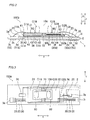
- the structure of a three-phase inverter device 100 including power modules 100a, 100b, and 100c according to a first embodiment is now described with reference to Fig. 1 .
- the power modules 100a to 100c are examples of the "power converter” in the present invention.
- the three-phase inverter device 100 is an example of the "power converter” in the present invention or the "three-phase inverter circuit" in the present invention.
- the three power modules 100a, 100b, and 100c performing U-phase, V-phase, and W-phase power conversion, respectively, are electrically connected in parallel to each other, whereby the three-phase inverter device 100 is configured.
- These three power modules 100a to 100c are provided as separate devices and are connected to each other by unshown wires or the like formed of metal wires.
- the power modules 100a, 100b, and 100c include half-bridge circuits 101a, 101b, and 101c configured to perform U-phase, V-phase, and W-phase power conversion, respectively and snubber capacitors 10a, 10b, and 10c electrically connected in parallel to the half-bridge circuits 101a, 101b, and 101c, respectively.
- Each of the half-bridge circuits 101a, 101b, and 101c is configured to include two switch elements (a first switch element 11a and a second switch element 12a, a first switch element 11b and a second switch element 12b, or a first switch element 11c and a second switch element 12c) electrically connected in series with each other.
- the first switch elements 11a, 11b, and 11c and the second switch elements 12a, 12b, and 12c are examples of the "power conversion semiconductor element" in the present invention.
- Each of the first switch elements 11a, 11b, and 11c is constituted by a MOSFET (field-effect transistor) having three electrodes (a gate electrode G1a, G1b, or G1c, a source electrode S1a, S1b, or S1c, and a drain electrode D1a, D1b, or D1c).
- Each of the second switch elements 12a, 12b, and 12c is also constituted by a MOSFET having three electrodes (a gate electrode G2a, G2b, or G2c, a source electrode S2a, S2b, or S2c, and a drain electrode D2a, D2b, or D2c).
- the first switch elements 11a, 11b, and 11c and the second switch elements 12a, 12b, and 12c are configured to perform switching on the basis of control signals externally input through control terminals 51a, 51b, and 51c and control terminals 52a, 52b, and 52c, respectively, to convert direct-current power input through input terminals 53 and 54 into three-phase (U-phase, V-phase, and W-phase) alternating-current power. Furthermore, the first switch elements 11a, 11b, and 11c and the second switch elements 12a, 12b, and 12c are configured to output the alternating-current power obtained by the aforementioned conversion to an external portion through output terminals 55a, 55b, and 55c.
- the input terminals 53 and 54 are connected to a P-electrode (+V) and an N-electrode (-V) of an unshown direct-current power supply, respectively.
- the output terminals 55a, 55b, and 55c are connected to respective unshown motors or the like.
- the detailed structure of the power modules 100a, 100b, and 100c according to the first embodiment is now described with reference to Figs. 2 and 3 .
- the power modules 100a, 100b, and 100c have substantially the same structure, and hence only the power module 100a including the two switch elements (the first switch element 11a and the second switch element 12a) and the snubber capacitor 10a is described below.
- the power module 100a includes a substrate 1, the two switch elements (the first switch element 11a and the second switch element 12a), two connection conductors 31 and 32, and the snubber capacitor 10a.
- the substrate 1 is an example of the "first substrate” in the present invention.
- the connection conductors 31 and 32 are examples of the "first connection conductor” and the “second connection conductor” in the present invention, respectively.
- the substrate 1 is configured to include an insulating plate 2 and ten conductive patterns 3a, 3b, 3c, 3d, 3e, 3f, 3g, 3h, 3i, and 3j provided on the front surface (upper surface: surface along an arrow Z2) and the rear surface (lower surface: surface along arrow Z1) of the insulating plate 2.
- the insulating plate 2 is made of an insulator such as ceramic in the form of a flat plate.
- the conductive patterns 3a to 3j each are made of a conductor of copper, gold, silver, aluminum, or alloy containing those in the form of a flat plate.
- the conductive patterns 3a, 3c, 3e, 3g, and 3i and the conductive patterns 3b, 3d, 3f, 3h, and 3j are electrically connected to each other through columnar conductors 3k, 31, 3m, 3n, and 3o provided to pass through the insulating plate 2 from the upper surface (the surface along arrow Z2) to the lower surface (the surface along arrow Z1), respectively.
- the conductive pattern 3e is an example of the "first conductive pattern” in the present invention.
- the conductive pattern 3c is an example of the "second conductive pattern” in the present invention
- the conductive pattern 3d is an example of the "third conductive pattern” in the present invention.
- the conductive patterns 3a and 3i are examples of the "fourth conductive pattern” in the present invention
- the conductive patterns 3b and 3j are examples of the "fifth conductive pattern” in the present invention.
- the conductive patterns 3a, 3c, 3e, 3g, and 3i and the conductive patterns 3b, 3d, 3f, 3h, and 3j, respectively, may be electrically connected to each other through hollow conductors like through vias, not the columnar conductors 3k, 31, 3m, 3n, and 3o.
- the first switch element 11a and the second switch element 12a are aligned in a direction X on the front surface (upper surface: surface along arrow Z2) of the substrate 1.
- a surface provided with the drain electrode D1a (D2a) of the first switch element 11a (second switch element 12a) is set to the front surface of the first switch element 11a (second switch element 12a)
- a surface provided with the gate electrode G1a (G2a) and the source electrode S1a (S2a) of the first switch element 11a (second switch element 12a) is set to the rear surface of the first switch element 11a (second switch element 12a).
- the first switch element 11a and the second switch element 12a are arranged such that the front surfaces and the rear surfaces thereof are oppositely oriented to each other, as shown in Fig. 2 .
- the drain electrode D1a provided on the front surface side of the first switch element 11a is arranged on the rear surface (lower surface: surface along arrow Z1) side of the connection conductor 31
- the drain electrode D2a provided on the front surface side of the second switch element 12a is arranged on the front surface (upper surface: surface along arrow Z2) side of the substrate 1.
- the gate electrode G1a and the source electrode S1a provided on the rear surface side of the first switch element 11a are arranged on the upper surface aside of the substrate 1
- the gate electrode G2a and the source electrode S2a provided on the rear surface side of the second switch element 12a are arranged on the lower surface side of the connection conductor 32.
- the drain electrode D1a of the first switch element 11a is bonded to the lower surface (surface along arrow Z1) of the connection conductor 31 through a bonding layer 41 made of solder or the like.
- the source electrode S1a and the gate electrode G1a of the first switch element 11a are bonded to the upper surfaces (surfaces along arrow Z2) of the conductive patterns 3c and 3e of the substrate 1 through a plurality of bumps 42.
- the drain electrode D1a of the second switch element 12a is bonded to the upper surface of the conductive pattern 3c of the substrate 1 through a bonding layer 43.
- the source electrode S2a of the second switch element 12a is bonded to the lower surface of the connection conductor 32 through a plurality of bumps 44.
- the gate electrode G2a of the second switch element 12a is electrically connected to the upper surface of the conductive pattern 3g of the substrate 10 through a wire 20 formed of a metal wire or the like.
- the source electrode S1a (gate electrode G1a) of the first switch element 11a and the conductive pattern 3c (3e) may be bonded to each other through a bonding layer made of solder or a bonding material other than solder, a plate-like conductor, or the like, not the bumps 42.
- the source electrode S1a (gate electrode G1a) of the first switch element 11a and the conductive pattern 3c (3e) may be bonded to each other only in a part of a region where the source electrode S1a (gate electrode G1a) of the first switch element 11a and the conductive pattern 3c (3e) are opposed to each other or may be bonded to each other in all of the region where the source electrode S1a (gate electrode G1a) of the first switch element 11a and the conductive pattern 3c (3e) are opposed to each other.
- Much the same is true on bonding between the source electrode S2a of the second switch element 12a and the connection conductor 32.
- connection conductors 31 and 32 are arranged above (on sides along arrow Z2 of) the first switch element 11a and the second switch element 12a, respectively.
- the connection conductors 31 and 32 each are made of a conductor of copper, gold, silver, aluminum, or alloy containing those in the form of a flat plate.
- the snubber capacitor 10a is arranged across the upper surfaces (surfaces along arrow Z2) of the two connection conductors 31 and 32. Specifically, one electrode C1a and the other electrode C2a of the snubber capacitor 10a are bonded to the upper surfaces of the connection conductors 31 and 32, respectively, through bonding materials 60 made of conductive adhesives such as solder or conductive paste (silver paste, for example).
- the connection conductors 31 and 32 are arranged to be held between the first switch element 11a and the snubber capacitor 10a and between the second switch element 12a and the snubber capacitor 10a, respectively.
- connection conductor 31 and the upper surface of the conductive pattern 3a of the substrate 1 are electrically connected to each other through a wire 20.
- the upper surface of the connection conductor 32 and the upper surface of the conductive pattern 3i of the substrate 1 are electrically connected to each other through a wire 20.
- a region between the upper surface of the substrate 1 and the lower surfaces (surfaces along arrow Z1) of the connection conductors 31 and 32 and a region between the upper surface of the substrate 1 and the lower surface of the snubber capacitor 10a are filled with a sealing resin 70 made of an epoxy resin, a silicone resin, or the like.
- the conductive pattern 3b provided on the lower surface (surface along arrow Z1) side of the substrate 1 is electrically connected to the drain electrode D1a of the first switch element 11a through the columnar conductor 3k, the conductive pattern 3a, the wire 20, the connection conductor 31, and the bonding layer 41. Therefore, the conductive pattern 3b constitutes the input terminal 53 (see Fig. 1 ) connected to the P-electrode (+V) of the unshown direct-current power supply.
- the conductive pattern 3d is electrically connected to the gate electrode G1a of the first switch element 11a through the columnar conductor 31, the conductive pattern 3c, and the bumps 42. Therefore, the conductive pattern 3d constitutes the control terminal 51a (see Fig. 1 ) into which the control signal for switching the first switch element 11a is input.
- the control terminal 51a is an example of the "first control terminal" in the present invention.
- the conductive pattern 3f provided on the lower surface (surface along arrow Z1) side of the substrate 1 is electrically connected to the source electrode S1a of the first switch element 11a through the columnar conductor 3m, the conductive pattern 3e, and the bumps 42 and is electrically connected to the drain electrode D2a of the second switch element 12a through the columnar conductor 3m, the conductive pattern 3e, and the bonding layer 43. Therefore, the conductive pattern 3f constitutes the output terminal 55a (see Fig. 1 ) connected to the unshown motor or the like.
- the conductive pattern 3h provided on the lower surface (surface along arrow Z1) side of the substrate 1 is electrically connected to the gate electrode G2a of the second switch element 12a through the columnar conductor 3n, the conductive pattern 3g, and the wire 20. Therefore, the conductive pattern 3h constitutes the control terminal 52a (see Fig. 1 ) into which the control signal for switching the second switch element 12a is input.
- the conductive pattern 3j is electrically connected to the source electrode S2a of the second switch element 12a through the columnar conductor 3o, the conductive pattern 3i, the wire 20, the connection conductor 32, and the bumps 44. Therefore, the conductive pattern 3j constitutes the input terminal 54 (see Fig. 1 ) connected to the N-electrode (-V) of the unshown direct-current power supply.
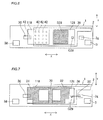
- a manufacturing process for the power module 100a according to the first embodiment is now described with reference to Figs. 2 to 7 .
- the substrate 1 provided with the ten conductive patterns 3a to 3j on the upper surface side (along arrow Z2) and lower surface side (along arrow Z1) of the insulating plate 2 is prepared, as shown in Figs. 4 and 5 .
- the upper surfaces (surfaces along arrow Z2) of the conductive patterns 3c and 3e of the substrate 1 and the gate electrode G1a and the source electrode S1a on the rear surface side of the first switch element 11a, respectively, are bonded to each other through the bumps 42 made of solder or the like, and the upper surface of the conductive pattern 3e and the drain electrode D2a on the front surface side of the second switch element 12a are bonded to each other through the bonding layer 43 made of solder or the like, as shown in Figs. 2 and 6 .
- connection conductors 31 and 32 in the form of a flat plate are arranged on the front surface side of the first switch element 11a and the rear surface side of the second switch element 12a, respectively, as shown in Figs. 2 and 7 .
- the drain electrode D1a on the front surface side of the first switch element 11a and the lower surface (surface along arrow Z1) of the connection conductor 31 are bonded to each other through the bonding layer 41, and the source electrode S2a and the gate electrode G2a on the rear surface side of the second switch element 12a and the lower surface of the connection conductor 31 are bonded to each other through the bumps 44.
- the snubber capacitor 10a is bonded through the bonding materials 60 across the upper surfaces (surfaces along arrow Z2) of the connection conductors 31 and 32, as shown in Figs. 2 and 3 .
- connection conductors 31 and 32 and the region between the upper surface of the substrate 1 and the lower surfaces (surfaces along arrow Z1) of the connection conductors 31 and 32 and the region between the upper surface of the substrate 1 and the lower surface of the snubber capacitor 10a are filled with the sealing resin 70.
- the upper surfaces of the connection conductors 31 and 32 and the upper surfaces of the conductive patterns 3a and 3i of the substrate 1, respectively, are electrically connected to each other through the wires 20.
- a solder resist is preferably applied to prescribed areas (see portions shown by diagonal lines in Figs. 5 to 7 , for example) in order to suppress spread of solder to unnecessary portions.
- connection conductor 31 (32) is arranged to be held between the snubber capacitor 10a and the first switch element 11a (second switch element 12a).
- the snubber capacitor 10a and the first switch element 11a (second switch element 12a) are electrically connected to each other through the single conductor (connection conductor 31 (32)), and hence a conduction path between the snubber capacitor 10a and the first switch element 11a (second switch element 12a) can be reduced in length. Consequently, a wiring inductance between the snubber capacitor 10a and the first switch element 11a (second switch element 12a) can be reduced.
- the drain electrode D1a on the front surface side of the first switch element 11a is arranged on the side of the connection conductor 31, and the source electrode S2a on the rear surface side of the second switch element 12a is arranged on the side of the connection conductor 32.
- the snubber capacitor 10a and the drain electrode D1a on the front surface side of the first switch element 11a can be easily electrically connected to each other through the connection conductor 31, and the snubber capacitor 10a and the source electrode S2a on the rear surface side of the second switch element 12a can be easily electrically connected to each other through the connection conductor 32.
- the conductive pattern 3e configured to connect the source electrode S1a on the rear surface side of the first switch element 11a and the drain electrode D2a on the front surface side of the second switch element 12a to each other is provided on the upper surface (surface along arrow Z2) of the substrate 1 on which the first switch element 11a and the second switch element 12a are arranged.
- the source electrode S1a on the rear surface side of the first switch element 11a and the drain electrode D2a on the front surface side of the second switch element 12a can be easily electrically connected to each other through the conductive pattern 3e of the substrate 1.
- connection conductors 31 and 32 are bonded to the snubber capacitor 10a through the bonding materials 60.
- the connection conductors 31 and 32 can be strongly bonded to the snubber capacitor 10a by the bonding materials 60.
- the region between the upper surface (surface along arrow Z2) of the substrate 1 and the lower surfaces (surfaces along arrow Z1) of the connection conductors 31 and 32 is filled with the sealing resin 70.
- connection conductors 31 and 32 are made of the conductor in the form of a flat plate. Furthermore, one electrode C1a and the other electrode C2a of the snubber capacitor 10a are connected to the upper surfaces (surfaces along arrow Z2) of the connection conductors 31 and 32, respectively, and the drain electrode D1a of the first switch element 11a and the source electrode S2a of the second switch element 12a are connected to the lower surfaces (surfaces along arrow Z1) of the connection conductors 31 and 32, respectively.
- the snubber capacitor 10a and the first switch element 11a and the second switch element 12a are bonded to the connection conductors 31 and 32 in the form of a flat plate, whereby bonding areas (plane areas) between the snubber capacitor 10a and the connection conductors 31 and 32 can be increased while bonding areas (plane areas) between the first switch element 11a and the connection conductor 31 and between the second switch element 12a and the connection conductor 32 can be increased. Consequently, bonding strength between the snubber capacitor 10a and the connection conductors 31 and 32 can be increased, and bonding strength between the first switch element 11a and the connection conductor 31 and between the second switch element 12a and the connection conductor 32 can be increased.
- the conductive patterns 3d and 3h, the conductive patterns 3b and 3j, and the conductive pattern 3f constituting the control terminals 51a and 52a, the input terminals 53 and 54, and the output terminal 55a, respectively, are provided on the lower surface (surface along arrow Z1) of the substrate 1.
- the control terminals 51a and 52a, the input terminals 53 and 54, and the output terminal 55a can be easily connected to external devices (the unshown direct-current power supply, the unshown motor, etc.), utilizing a region on the lower surface side of the substrate 1.
- the conductive pattern 3c is provided on the upper surface (surface along arrow Z2) of the substrate 1, and the conductive pattern 3d electrically connected to the conductive pattern 3c is provided on the lower surface (surface along arrow Z2) of the substrate 1. Furthermore, the conductive pattern 3c on the upper surface of the substrate 1 and the gate electrode G1a provided on the rear surface side of the first switch element 11a are connected to each other, and the conductive pattern 3d on the lower surface of the substrate 1 constitutes the control terminal 51a.
- the gate electrode G1a of the first switch element 11a and the control terminal 51a can be easily connected to each other, unlike the case where the gate electrode G1a of the first switch element 11a and the control terminal 51a into which the control signal is externally input are connected to each other by a wire or the like.
- a power module 200a according to a second embodiment is now described with reference to Figs. 8 to 16 .
- this second embodiment an example of arranging two switch elements (a first switch element 11a and a second switch element 12a) in a region (space) between two substrates (a first substrate 201 and a second substrate 205) arranged to be opposed to each other is described unlike the aforementioned first embodiment (see Fig. 2 ) in which the two switch elements (the first switch element 11a and the second switch element 12a) are arranged on the upper surface (surface along arrow Z2) of the single substrate 1.
- the power module 200a is an example of the "power converter" in the present invention.
- the structure of the power module 200a according to the second embodiment is described with reference to Figs. 8 to 15 .
- This power module 200a performs U-phase power conversion in a three-phase inverter device.
- two power modules power modules performing V-phase and W-phase power conversion
- the power module 200a performing U-phase power conversion is described below for simplification.
- the power module 200a includes the first substrate 201, the two switch elements (the first switch element 11a and the second switch element 12a), the second substrate 205, and a snubber capacitor 10a.
- the first substrate 201 is configured to include an insulating plate 202 in the form of a flat plate, conductive patterns 203a, 203b, and 203c provided on the upper surface (surface along arrow Z2) and lower surface (surface along arrow Z1) of the insulating plate 202, two insulating plates 204 provided to protrude from the upper surfaces of the conductive patterns 203a and 203b, and conductive patterns 203d and 203e provided on the upper surfaces of the two insulating plates 204.
- the insulating plates 202 and 204 each are made of an insulator such as ceramic.
- the conductive patterns 203a to 203e each are made of a conductor of copper, gold, silver, aluminum, or alloy containing those in the form of a flat plate.
- the conductive pattern 203a and the conductive pattern 203d are electrically connected to each other through a columnar conductor 203f provided to pass through the insulating plate 204. Furthermore, the conductive pattern 203b and the conductive pattern 203e are electrically connected to each other through a columnar conductor 203g provided to pass through the insulating plate 204.
- the conductive pattern 203b is an example of the "first conductive pattern" in the present invention.
- the two insulating plates 204 arranged in the vicinity of both ends of the first substrate 201 in a direction X constitute two protruding portions 204a protruding upward (along arrow Z2) from the upper surface (surface along arrow Z2) of the first substrate 201, as shown in Figs. 8 and 12 .
- a space formed by the inner surfaces of these two protruding portions 204a and the upper surface of the insulating plate 202 constitutes a recess portion 204b.
- the second substrate 205 is arranged above (on a side along arrow Z2 of) the first substrate 201. Specifically, the lower surface (surface along arrow Z1) of the second substrate 205 is bonded to the upper surfaces of the conductive patterns 203d and 203e provided on the upper surfaces (surfaces along arrow Z2) of the two insulating plates 204 (protruding portions 204a) through bonding layers 45 made of solder or the like.
- the second substrate 205 is configured to include an insulating plate 206 in the form of a flat plate and conductive patterns 207a, 207b, 207c, 207d, 207e, 207f, 207g, 207h, 207i, and 207j provided on the upper surface (surface along arrow Z2) and lower surface (surface along arrow Z1) of the insulating plate 206.
- the insulating plate 206 is made of an insulator such as ceramic.
- the conductive patterns 207a to 207i each are made of a conductor of copper, gold, silver, aluminum, or alloy containing those in the form of a flat plate.
- the conductive patterns 207a, 207c, 207e, 207g, and 207i and the conductive patterns 207b, 207d, 207f, 207h, and 207j are electrically connected to each other through columnar conductors 207k, 2071, 207m, 207n, and 207o provided to pass through the insulating plate 2 from the upper surface (the surface along arrow Z2) to the lower surface (the surface along arrow Z1), respectively.
- the conductive patterns 207c and 207e are examples of the "sixth conductive pattern” in the present invention, and the conductive patterns 207d and 207f are examples of the "seventh conductive pattern" in the present invention.
- the conductive pattern 207g is an example of the "eighth conductive pattern” in the present invention
- the conductive pattern 207h is an example of the "ninth conductive pattern” in the present invention.
- the first switch element 11a and the second switch element 12a having the same structure as those according to the aforementioned first embodiment are aligned in the direction X in a region between the upper surface (surface along arrow Z2) of the first substrate 201 and the lower surface (surface along arrow Z1) of the second substrate 205 (a space in the aforementioned recess portion 204b formed by the inner surfaces of the insulating plates 204 and the conductive patterns 203d and 203e and the upper surface of the first substrate 201).
- the first switch element 11a and the second switch element 12a are arranged such that the front surfaces and the rear surfaces thereof are oppositely oriented to each other, similarly to the aforementioned first embodiment.
- a drain electrode D1a provided on the front surface side of the first switch element 11a is bonded to the lower surface (surface along arrow Z1) of the conductive pattern 207d of the second substrate 205 through a bonding layer 41 made of solder or the like.
- a source electrode S1a and a gate electrode G1a provided on the rear surface side of the first switch element 11a are bonded to the upper surfaces (surfaces along arrow Z2) of the conductive patterns 203a and 203b of the first substrate 201, respectively, through bumps 42 made of solder or the like.
- a drain electrode D2a provided on the front surface side of the second switch element 12a is bonded to the upper surface (surface along arrow Z2) of the conductive pattern 203b of the first substrate 201 through a bonding layer 43.
- a source electrode S2a and a gate electrode G2a provided on the rear surface side of the second switch element 12a are bonded to the lower surfaces (surfaces along arrow Z1) of the conductive patterns 207f and 207h of the second substrate 205 through bumps 44, respectively.
- the conductive patterns 207d and 207f of the second substrate 205 are arranged above (on sides along arrow Z2 of) the first switch element 11a and the second switch element 12a, respectively.
- the snubber capacitor 10a is arranged across the upper surfaces (surfaces along arrow Z2) of the conductive patterns 207c and 207e of the second substrate 205.
- one electrode C1a and the other electrode C2a of the snubber capacitor 10a are bonded to the upper surfaces of the conductive patterns 207c and 207e of the second substrate 205, respectively, through bonding materials 60 made of conductive adhesives such as solder or conductive paste (silver paste, for example).
- the conductive patterns 207c and 207d and the columnar conductor 2071 between the conductive patterns 207c and 207d are arranged to be held between the first switch element 11a and one electrode C1a of the snubber capacitor 10a.
- the conductive patterns 207e and 207f and the columnar conductor 207m between the conductive patterns 207e and 207f are arranged to be held between the second switch element 12a and the other electrode C2a of the snubber capacitor 10a.
- the conductive patterns 207c and 207d and the columnar conductor 2071 are examples of the "first connection conductor" in the present invention.
- the conductive patterns 207e and 207f and the columnar conductor 207m are examples of the "second connection conductor" in the present invention.
- a space between the upper surface (surface along arrow Z2) of the first substrate 201 and the lower surface (surface along arrow Z1) of the second substrate 205 is filled with a sealing resin 70, similarly to the aforementioned first embodiment.
- the conductive pattern 207a provided on the upper surface (surface along arrow Z2) side of the second substrate 205 is electrically connected to the gate electrode G1a of the first switch element 11a through the columnar conductor 207k, the conductive pattern 207b, the bonding layer 45, the conductive pattern 203d of the first substrate 201, the columnar conductor 203f, the conductive pattern 203a, and the bump 42. Therefore, the conductive pattern 207a constitutes a control terminal 51a (see Fig. 1 ) into which a control signal for switching the first switch element 11a is input.
- the conductive pattern 207c provided on the upper surface (surface along arrow Z2) side of the second substrate 205 is electrically connected to the drain electrode D1a of the first switch element 11a through the columnar conductor 2071, the conductive pattern 207d, and the bonding layer 41. Therefore, the conductive pattern 207c constitutes an input terminal 53 (see Fig. 1 ) connected to a P-electrode (+V) of an unshown direct-current power supply. Furthermore, the conductive pattern 207e of the second substrate 205 is electrically connected to the source electrode S2a of the second switch element 12a through the columnar conductor 207m, the conductive pattern 207f, and the bumps 44. Therefore, the conductive pattern 207e constitutes an input terminal 54 (see Fig. 1 ) connected to an N-electrode (-V) of the unshown direct-current power supply.
- the conductive pattern 207g provided on the upper surface (surface along arrow Z2) side of the second substrate 205 is connected to the gate electrode G2a of the second switch element 12a through the columnar conductor 207n, the conductive pattern 207h, and the bump 44. Therefore, the conductive pattern 207g constitutes a control terminal 52a (see Fig. 1 ) into which a control signal for switching the second switch element 12a is input.
- the conductive pattern 207i of the second substrate 205 is electrically connected to the source electrode S1a of the first switch element 11a and the drain electrode D2a of the second switch element 12a through the columnar conductor 207o, the conductive pattern 207j, the bonding layer 45, the conductive pattern 203e of the first substrate 201, the columnar conductor 203g, the conductive pattern 203b, and the bonding layer 43. Therefore, the conductive pattern 207i constitutes a U-phase output terminal 55a (see Fig. 1 ) connected to an unshown motor or the like.
- the substrate 201 provided with the conductive patterns 203a to 203c, the two insulating plates 204, and the two conductive patterns 203d and 203e on the upper surface side (along arrow Z2) and lower surface side (along arrow Z1) of the insulating plate 202 is prepared, as shown in Figs. 10 and 11 .
- the upper surfaces (surfaces along arrow Z2) of the conductive patterns 203a and 203b of the first substrate 201 and the gate electrode G1a and the source electrode S1a on the rear surface side of the first switch element 11a, respectively, are bonded to each other through the bumps 42 made of solder or the like, as shown in Fig. 12 .
- the second substrate 205 provided with the ten conductive patterns 207a to 207j on the upper surface side (along arrow Z2) and lower surface side (along arrow Z1) of the insulating plate 206 is prepared, as shown in Figs. 13 and 14 .
- the lower surfaces (surfaces along arrow Z1) of the conductive patterns 207f and 207h of the second substrate 205 and the source electrode S2a and the gate electrode G2a on the rear surface side of the second switch element 12a, respectively, are bonded to each other through the bumps 44, as shown in Fig. 15 .
- the drain electrode D1a of the first switch element 11a bonded to the upper surface (surface along arrow Z2) of the first substrate 201 and the lower surface (surface along arrow Z1) of the conductive pattern 207d of the second substrate 205 are bonded to each other through the bonding layer 41 made of solder or the like. Furthermore, the drain electrode D2a of the second switch element 12a mounted on the lower surface of the second substrate 205 and the upper surface of the conductive pattern 203b of the first substrate 201 are bonded to each other through the bonding layer 43.
- the space between the upper surface (surface along arrow Z2) of the first substrate 201 and the lower surface (surface along arrow Z1) of the second substrate 205 is filled with the sealing resin 70, as shown in Fig. 8 . Furthermore, the snubber capacitor 10a is bonded to the upper surfaces of the conductive patterns 207c and 207e of the second substrate 205 through the bonding materials 60.
- a solder resist is preferably applied to prescribed areas (see portions shown by diagonal lines in Figs. 11 , 13, and 14 , for example) in order to suppress spread of solder to unnecessary portions.
- high temperature solder can be employed for the bumps 42 (44) and low temperature solder can be employed for the bonding layers 45 in order to suppress melting of the bumps 42 (44) for bonding the first substrate 201 (second substrate 205) and the first switch element 11a (second switch element 12a) to each other.
- the conductive patterns 207c and 207e are provided on the upper surface (surface along arrow Z2) of the second substrate 205, and the conductive patterns 207d and 207f electrically connected to the conductive patterns 207c and 207e, respectively, are provided on the lower surface (surface along arrow Z1) of the second substrate 205. Furthermore, the upper surfaces of the conductive patterns 207c and 207e are connected to one electrode C1a and the other electrode C2a of the snubber capacitor 10a, respectively, and the lower surfaces of the conductive patterns 207d and 207f are connected to the drain electrode D1a of the first switch element 11a and the source electrode D2a of the second switch element 12a, respectively.
- conduction paths between the drain electrode D1a of the first switch element 11a and one electrode C1a of the snubber capacitor 10a and between the source electrode S2a of the second switch element 12a and the other electrode C2a of the snubber capacitor 10a can be easily reduced in length with the second substrate 205 including the conductive patterns 207c to 207f.
- the conductive pattern 207g is provided on the upper surface (surface along arrow Z2) side of the second substrate 205, and the conductive pattern 207h electrically connected to the conductive pattern 207g is provided on the lower surface (surface along arrow Z2) side of the second substrate 205. Furthermore, the conductive pattern 207h and the gate electrode G1a on the rear surface side of the second switch element 12a are connected to each other, and the conductive pattern 207g constitutes the control terminal 52a.
- the gate electrode G2a of the second switch element 12a and the control terminal 52a can be easily connected to each other, unlike the case where the gate electrode G2a of the second switch element 12a and the control terminal 52a into which the control signal is externally input are connected to each other by a wire or the like.
- the conductive patterns 207c and 207e provided on the upper surface (surface along arrow Z2) side of the second substrate 205 connected to the snubber capacitor 10a constitute the input terminals 53 and 54.
- the input terminals 53 and 54 can be easily connected to the unshown direct-current power supply, utilizing a region on the upper surface side of the second substrate 205.
- the recess portion 204b configured to arrange the first switch element 11a and the second switch element 12a and the protruding portions 204a (insulating plates 204) adjacent to the recess portion 204b are provided on the upper surface (surface along arrow Z2) side of the first substrate 201 arranged to be opposed to the lower surface (surface along arrow Z1) of the second substrate 205. Furthermore, the conductive patterns 203d and 203e provided on the protruding portions 204a (insulating plates 204) of the first substrate 201 and the lower surfaces of the conductive patterns 207b and 207j of the second substrate 205, respectively, are bonded to each other.
- the first switch element 11a and the second switch element 12a can be easily arranged between the upper surface of the first substrate 201 and the lower surface of the second substrate 205, utilizing the space constituted by the recess portion 204b of the first substrate 201.
- the protruding portions 204a provided in the first substrate 210 can stably support the second substrate 205 from below.
- a power module 300a according to a third embodiment is now described with reference to Figs. 17 and 18 .
- this third embodiment an example of providing heat radiating plates 81 and 82 having a heat radiating function on the upper surface side of a snubber capacitor 10a is described unlike the aforementioned first embodiment in which nothing is provided on the upper surface side (side along arrow Z2) of the snubber capacitor 10a.
- the power module 300a is an example of the "power converter” in the present invention.
- the heat radiating plates 81 and 82 are examples of the "heat radiating member" in the present invention.
- the power module 200a performs U-phase power conversion in a three-phase inverter device.
- two power modules power modules performing V-phase and W-phase power conversion
- the power module 300a performing U-phase power conversion is described below for simplification.
- the power module 300a includes a substrate 1, two switch elements (a first switch element 11a and a second switch element 12a), two connection conductors 31 and 32, the snubber capacitor 10a, and the two heat radiating plates 81 and 82.
- the heat radiating plates 81 and 82 each are made of a conductor of metal such as copper excellent in thermal conductivity in the form of a flat plate.
- the heat radiating plates 81 and 82 are arranged on the upper surface side (side along arrow Z2) of the snubber capacitor 10a in correspondence to the connection conductors 31 and 32 arranged to be held between the snubber capacitor 10a and the first switch element 11a and between the snubber capacitor 10a and the second switch element 12a, respectively.
- the lower surface (surface along arrow Z1) of the heat radiating member 81 and the upper surface (surface along arrow Z2) of one electrode C1a of the snubber capacitor 10a are bonded to each other through a bonding material 61 made of a conductive adhesive such as solder or conductive paste (silver paste, for example).
- the lower surface of the heat radiating plate 82 and the upper surface of the other electrode C2a of the snubber capacitor 10a are bonded to each other through a bonding material 61.
- the remaining structure of the third embodiment is similar to that of the aforementioned first embodiment.
- the heat radiating members 81 and 82 are provided on the side (side along arrow Z2) of the snubber capacitor 10a opposite to the connection conductors 31 and 32.
- the heat radiating members 81 and 81 can easily radiate heat generated from the snubber capacitor 10a.
- a power module 400 The structure of a power module 400 according to a fourth embodiment is now described with reference to Figs. 19 and 20 .
- a single device power module (three-phase inverter device) 400
- U-phase, V-phase, and W-phase power conversion is performed by the three devices (power modules 100a to 100c) provided separately from each other.
- the power module 400 is an example of the "power converter" in the present invention.
- the power module 400 includes a substrate 401, six switch elements (first switch elements 11a to 11c and second switch elements 12a to 12c), two connection conductors 431 and 432, and three snubber capacitors 10a to 10c.
- the substrate 401 is an example of the "first substrate" in the present invention.
- the substrate 401 is configured to include an insulating plate 402 in the form of a flat plate, nine conductive patterns (three conductive patterns 403a, three conductive patterns 403b, and three conductive patterns 403c) provided on the upper surface (surface along arrow Z2) of the insulating plate 402, and nine conductive patterns (three conductive patterns 403d, three conductive patterns 403e, and three conductive patterns 403f) provided on the lower surface (surface along arrow Z1) of the insulating plate 402.
- the conductive patterns 403a, 403b, and 403c and the conductive patterns 403d, 403e, and 403f are electrically connected to each other through columnar conductors 403g, 403h, and 403i provided to pass through the insulting plate 402 from the upper surface to the lower surface, respectively.
- the three conductive patterns 403c are examples of the "first conductive pattern” in the present invention.
- the three conductive patterns 403a are examples of the "second conductive pattern” in the present invention, and the three conductive patterns 403b are examples of the "third conductive pattern" in the present invention.
- the two switch elements (the first switch element 11a and the second switch element 12a) configured to perform U-phase power conversion are aligned in a direction X on the upper surfaces of the conductive patterns 403a and 403c provided in the vicinity of an end along arrow Y1 (see Fig. 19 ) of the upper surface (surface along arrow Z2) of the substrate 401.
- These two switch elements (the first switch element 11a and the second switch element 12a) are arranged such that the front surfaces and the rear surfaces thereof are oppositely oriented to each other, similarly to the aforementioned first embodiment.
- a gate electrode G1a on the rear surface side of the first switch element 11a is bonded to the upper surface of the conductive pattern 403a of the substrate 401 through a bump 42.
- a source electrode S1a on the rear surface side of the first switch element 11a and a drain electrode D2a on the front surface side of the second switch element 12a are bonded to the upper surface of the conductive pattern 403c of the substrate 401 through bumps 42 and a bonding layer 44, respectively.
- first switch element 11b (11c) and the second switch element 12b (12c) configured to perform V-phase (W-phase) power conversion are aligned in the direction X on the upper surfaces of the conductive patterns 403a and 403c provided in the vicinity of a central portion in a direction Y (in the vicinity of an end along arrow Y2) (see Fig. 19 ) of the upper surface (surface along arrow Z2) of the substrate 401.
- the first switch element 11b (11c) and the second switch element 12b (12c) are arranged such that the front surfaces and the rear surfaces thereof are oppositely oriented to each other.
- a gate electrode G1b (G1c) on the rear surface side of the first switch element 11b (11c) is bonded to the upper surface of the conductive pattern 403a of the substrate 401 through a bump 42.
- a source electrode S1b (S1c) on the rear surface side of the first switch element 11b (11c) and a drain electrode D2b (D2c) on the front surface side of the second switch element 12b (12c) are bonded to the upper surface of the conductive pattern 403c of the substrate 401 through bumps 42 and a bonding layer 44, respectively.
- connection conductors 431 and 432 each are made of a conductor in the form of a flat plate extending in the direction Y, as shown in Fig. 19 .
- the connection conductors 431 and 432 are arranged across the three first switch elements 11a to 11c and the three second switch elements 12a to 12c in common, respectively.
- respective drain electrodes D1a to D1c of the three first switch elements 11a to 11c are bonded to the lower surface (surface along arrow Z1) of the connection conductor 431 through bonding layers 41, as shown in Fig. 20 .
- Respective source electrodes S2a to S2c on the rear surface sides of the three second switch elements 12a to 12c are bonded to the lower surface of the connection conductor 432 through bumps 44.
- connection conductors 431 and 432 are also arranged across the three snubber capacitors 10a to 10c in common in addition to the aforementioned six switch elements (the three first switch elements 11a to 11c and the three second switch elements 12a to 12c).
- the snubber capacitors 10a, 10b, and 10c are arranged across the upper surfaces (surfaces along arrow Z2) of the two connection conductors 431 and 432 in correspondence to the first switch element 11a and the second switch element 12a, the first switch element 11b and the second switch element 12b, and the first switch element 11c and the second switch element 12c, respectively.
- the snubber capacitors 10a to 10c are bonded to the upper surfaces of the connection conductors 431 and 432 through bonding materials 60.
- connection conductors 431 and 432 are arranged to be held between the three first switch elements 11a to 11c and the three snubber capacitors 10a to 10c and between the three second switch elements 12a to 12c and the three snubber capacitors 10a to 10c.
- the connection conductors 431 and 432 are examples of the "first connection conductor” and the "second connection conductor” in the present invention, respectively.
- a region between the upper surface (surface along arrow Z2) of the substrate 401 and the lower surfaces (surfaces along arrow Z1) of the connection conductors 431 and 432 and a region between the upper surface of the substrate 401 and the lower surfaces of the snubber capacitors 10a to 10c are filled with sealing resins 70, similarly to the aforementioned first embodiment.
- Gate electrodes G2a to G2c of the second switch elements 12a to 12c are electrically connected to the respective upper surfaces of the three conductive patterns 403e of the substrate 401 through wires 20.
- the three respective conductive patterns 403b provided on the lower surface (surface along arrow Z1) side of the substrate 401 are electrically connected to the gate electrodes G1a to G1c of the first switch elements 11a to 11c through the columnar conductors 403g, the conductive patterns 403a, and the bumps 42, as shown in Fig. 20 . Therefore, the three conductive patterns 403b constitute three control terminals 51a to 51c (see Fig. 1 ) into which control signals for switching the first switch elements 11a to 11c are input.
- the three respective conductive patterns 403d provided on the lower surface (surface along arrow Z1) side of the substrate 401 are electrically connected to the source electrodes S1a to S1c of the first switch elements 11a to 11c through the columnar conductors 403h, the conductive patterns 403c, and the bumps 43 and are electrically connected to the drain electrodes D2a to D2c of the second switch elements 12a to 12c through the columnar conductors 403h, the conductive patterns 403c, and the bonding layers 43. Therefore, the three respective conductive patterns 403d constitute U-phase, V-phase, and W-phase output terminals 55a to 55c (see Fig. 1 ) connected to unshown motors or the like.
- the three respective conductive patterns 403f provided on the lower surface (surface along arrow Z1) side of the substrate 401 are electrically connected to the gate electrodes G2a to G2c of the second switch elements 12a to 12c through the columnar conductors 403i, the conductive patterns 403e and the wires 20. Therefore, the three respective conductive patterns 403f constitute three control terminals 52a to 52c (see Fig. 1 ) into which control signals for switching the second switch elements 12a to 12c are input.
- connection conductor 431 is electrically connected to the drain electrodes D1a to D1c of the first switch elements 11a to 11c through the bonding layers 41, and the connection conductor 432 is electrically connected to the source electrodes S2a to S2c of the second switch elements 12a to 12c through the bumps 44. Therefore, the connection conductors 431 and 432 constitute an input terminal 53 (see Fig. 1 ) connected to a P-electrode (+V) of an unshown direct-current power supply and an input terminal 54 (see Fig. 1 ) connected to an N-electrode (-V) thereof, respectively.
- the single power module (three-phase inverter device) 400 is configured by connecting the three first switch elements 11a to 11c and the three second switch elements 12a to 12c to the three snubber capacitors 10a to 10c in parallel to each other.
- the number of components can be reduced unlike the case where a total of three power modules of a power module constituted by the first switch element 11a, the second switch element 12a, and the snubber capacitor 10a, a power module constituted by the first switch element 11b, the second switch element 12b, and the snubber capacitor 10b, and a power module constituted by the first switch element 11c, the second switch element 12c, and the snubber capacitor 10c are provided separately from each other (the case where the three-phase inverter device 100 (see Fig. 1 ) is constituted by the three power modules 100a to 100c provided separately from each other, as in the aforementioned first embodiment, for example), and hence the structure of the device can be simplified.
- connection conductors 431 and 432 are arranged across the three first switch elements 11a to 11c, the three second switch elements 12a to 12c, and the three snubber capacitors 10a to 10c in common.
- the number of components can be reduced unlike the case where three respective connection conductors are provided separately for the first switch element 11a, the second switch element 12a, and the snubber capacitor 10a, for the first switch element 11b, the second switch element 12b, and the snubber capacitor 10b, and for the first switch element 11c, the second switch element 12c, and the snubber capacitor 10c, and hence the structure of the device can be simplified.
- the present invention is also applicable to a power converter other than the three-phase inverter device, so far as the same includes switch elements and snubber capacitors.
- the present invention is not restricted to this.
- two or more snubber capacitors may be provided in the single power module.
- two snubber capacitors 10d and 10e (10f and 10g) may be provided in a single power module 110a (210a).
- the power module 110a (210a) is an example of the "power converter" in the present invention.
- the two snubber capacitors 10d and 10e are provided in the single power module 110a. These two snubber capacitors 10d and 10e are aligned in a direction Y across the upper surfaces (surfaces along arrow Z2) of two connection conductors 31 and 32. Also according to this modification shown in Fig. 21 , the connection conductors 31 and 32 are arranged to be held between a first switch element 11a and the snubber capacitors 10d and 10e and between a second switch element 12a and the snubber capacitors 10d and 10e, respectively, similarly to the aforementioned first embodiment shown in Fig. 2 .
- the two snubber capacitors 10f and 10g are provided in the single power module 210a. These two snubber capacitors 10f and 10g are aligned in a direction Y across the upper surfaces (surfaces along arrow Z2) of two conductive patterns 207c and 207e provided on the upper surface (surface along arrow Z2) side of a second substrate 205. Also according to this modification shown in Fig.
- conductive patterns 207c and 207d of the second substrate 205 and a columnar conductor 2071 are arranged to be held between a first switch element 11a and the snubber capacitors 10f and 10g, similarly to the aforementioned second embodiment shown in Fig. 8 . Furthermore, conductive patterns 207e and 207f of the second substrate 205 and a columnar conductor 207m are arranged to be held between a second switch element 12a and the snubber capacitors 10f and 10g.
- the single power module 110a (210a) is provided with the two snubber capacitors 10d and 10e (10f and 10g), whereby more surge voltage can be absorbed, as compared with the case where the single power module is provided with a single snubber capacitor (the case of the aforementioned first or second embodiment).
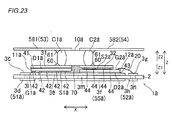
- heat radiating plates 581 and 582 may be employed as the input terminals 53 and 54 (see Fig. 1 ), respectively, as in a modification of the third embodiment shown in Fig. 23 .
- the heat radiating plates 581 and 582 are examples of the "heat radiating member" in the present invention.
- the heat radiating plates 581 and 582 each are made of a conductor of metal such as copper excellent in thermal conductivity in the form of a flat plate, similarly to the aforementioned third embodiment.
- the heat radiating plate 581 is electrically connected to a drain electrode D1a of a first switch element 11a through a bonding material 61, one terminal C1a of a snubber capacitor 10a, a bonding material 60, a connection conductor 31, and a bonding layer 41.
- the heat radiating plate 581 constitutes an input terminal 53 (see Fig. 1 ) connected to a P-electrode (+V) of an unshown direct-current power supply.
- the heat radiating plate 582 is electrically connected to a source electrode S2a of a second switch element 12a through a bonding material 61, the other electrode C2a of the snubber capacitor 10a, a bonding material 60, a connection conductor 32, and bumps 44.
- the heat radiating plate 582 constitutes an input terminal 54 (see Fig. 1 ) connected to an N-electrode (-V) of the unshown direct-current power supply.
- the heat radiating plates 581 and 582 are employed as the input terminals 53 and 54 (see Fig. 1 ), whereby conductive patterns (the aforementioned conductive patterns 3b and 3j according to the third embodiment shown in Fig. 17 ) dedicated for constituting the input terminals 53 and 54 may not be provided in a substrate 1a, and hence the structure of the device can be simplified.
- the present invention is not restricted to this.
- the heat radiating member may be made of a member other than metal, so far as the member is excellent in thermal conductivity.
- MOSFET field-effect transistor
- IGBT insulated gate bipolar transistor
Landscapes
- Engineering & Computer Science (AREA)
- Power Engineering (AREA)
- Inverter Devices (AREA)
Applications Claiming Priority (1)
| Application Number | Priority Date | Filing Date | Title |
|---|---|---|---|
| PCT/JP2012/052119 WO2013114565A1 (ja) | 2012-01-31 | 2012-01-31 | 電力変換装置および電力変換装置の製造方法 |
Publications (2)
| Publication Number | Publication Date |
|---|---|
| EP2811642A1 true EP2811642A1 (de) | 2014-12-10 |
| EP2811642A4 EP2811642A4 (de) | 2015-10-07 |
Family
ID=48904644
Family Applications (1)
| Application Number | Title | Priority Date | Filing Date |
|---|---|---|---|
| EP12867525.3A Withdrawn EP2811642A4 (de) | 2012-01-31 | 2012-01-31 | Leistungswandler und verfahren zur herstellung eines leistungswandlers |
Country Status (4)
| Country | Link |
|---|---|
| US (1) | US20140334203A1 (de) |
| EP (1) | EP2811642A4 (de) |
| CN (1) | CN104081646A (de) |
| WO (1) | WO2013114565A1 (de) |
Cited By (3)
| Publication number | Priority date | Publication date | Assignee | Title |
|---|---|---|---|---|
| WO2018037984A1 (en) * | 2016-08-22 | 2018-03-01 | Neturen Co., Ltd. | Power semiconductor module, snubber circuit, and induction heating power supply apparatus |
| DE102022208031A1 (de) | 2022-08-03 | 2024-02-08 | Siemens Aktiengesellschaft | Halbleiterbauelement |
| DE102023002782A1 (de) | 2023-07-07 | 2025-01-09 | Mercedes-Benz Group AG | Leistungsversorgungseinrichtung für ein Kraftfahrzeug, insbesondere einen Kraftwagen, sowie Kraftfahrzeug |
Families Citing this family (22)
| Publication number | Priority date | Publication date | Assignee | Title |
|---|---|---|---|---|
| JP6020572B2 (ja) * | 2012-08-29 | 2016-11-02 | 株式会社安川電機 | 電力変換装置 |
| JP5867472B2 (ja) * | 2013-09-17 | 2016-02-24 | 株式会社安川電機 | 電力変換装置 |
| US9077335B2 (en) * | 2013-10-29 | 2015-07-07 | Hrl Laboratories, Llc | Reduction of the inductance of power loop and gate loop in a half-bridge converter with vertical current loops |
| JP6413396B2 (ja) * | 2014-06-30 | 2018-10-31 | 富士電機株式会社 | 電力変換装置及び電動モータ |
| WO2016103324A1 (ja) | 2014-12-22 | 2016-06-30 | 三菱電機株式会社 | 電力変換装置および電力用半導体モジュール |
| JP6358129B2 (ja) * | 2015-02-26 | 2018-07-18 | 株式会社デンソー | 電力変換装置 |
| JP6497286B2 (ja) * | 2015-09-18 | 2019-04-10 | 株式会社デンソー | 半導体モジュール |
| EP3298629A4 (de) | 2015-10-09 | 2019-01-09 | HRL Laboratories, LLC | Monolithisch integrierter gan-auf-saphir-leistungswandler |
| WO2017187577A1 (ja) * | 2016-04-27 | 2017-11-02 | 三菱電機株式会社 | インバータ装置 |
| JP6360865B2 (ja) * | 2016-09-28 | 2018-07-18 | 高周波熱錬株式会社 | スナバ回路及びパワー半導体モジュール並びに誘導加熱用電源装置 |
| JP6759874B2 (ja) * | 2016-09-01 | 2020-09-23 | 富士電機株式会社 | 電力変換装置 |
| US10916531B2 (en) * | 2016-11-24 | 2021-02-09 | Sumitomo Electric Industries, Ltd. | Semiconductor module |
| JP7038632B2 (ja) * | 2018-09-12 | 2022-03-18 | 三菱電機株式会社 | 半導体装置、及び、半導体装置の製造方法 |
| EP3720259B1 (de) * | 2019-04-03 | 2023-05-31 | ABB Schweiz AG | Schaltmodulanordnung und verfahren zur herstellung davon |
| JP7396041B2 (ja) * | 2019-12-27 | 2023-12-12 | ニデックパワートレインシステムズ株式会社 | モータ駆動用制御基板、及び電動オイルポンプ |
| JP2021182575A (ja) * | 2020-05-18 | 2021-11-25 | 現代自動車株式会社Hyundai Motor Company | 半導体装置内部スナバ回路接続構造及びこれを用いたパワーモジュール構造 |
| DE102020207701A1 (de) * | 2020-06-22 | 2021-12-23 | Zf Friedrichshafen Ag | Leistungsmodul zum Betreiben eines Elektrofahrzeugantriebs mit einem Zwischenkreiskondensator |
| DE102021211409A1 (de) * | 2021-10-11 | 2023-04-13 | Zf Friedrichshafen Ag | Inverteraufbau eines Elektronikmoduls für einen Elektroantrieb eines Fahrzeugs |
| DE102021211519B4 (de) | 2021-10-13 | 2023-11-02 | Vitesco Technologies Germany Gmbh | Elektronische Baugruppe |
| DE102023109216A1 (de) * | 2023-04-12 | 2024-10-17 | Dr. Ing. H.C. F. Porsche Aktiengesellschaft | Verfahren und Schaltung zu einem Pulswechselrichter mit integrierter DCDCWandelfunktion |
| WO2025032244A1 (en) * | 2023-08-10 | 2025-02-13 | Lotus Microsystems Aps | Stacked power converter assembly with thermally conductive elements |
| DE102024202527A1 (de) * | 2024-03-18 | 2025-09-18 | Zf Friedrichshafen Ag | Stapelbare Leistungshalbleiter-Baugruppe |
Family Cites Families (17)
| Publication number | Priority date | Publication date | Assignee | Title |
|---|---|---|---|---|
| JP3501685B2 (ja) * | 1999-06-04 | 2004-03-02 | 三菱電機株式会社 | 電力変換装置 |
| JP4878424B2 (ja) * | 2001-08-09 | 2012-02-15 | 東芝三菱電機産業システム株式会社 | 電力変換装置 |
| US7045884B2 (en) * | 2002-10-04 | 2006-05-16 | International Rectifier Corporation | Semiconductor device package |
| DE10326321A1 (de) * | 2003-06-11 | 2005-01-13 | Compact Dynamics Gmbh | Elektronische Baugruppe zum Schalten elektrischer Leistung |
| JP2005150454A (ja) * | 2003-11-17 | 2005-06-09 | Yaskawa Electric Corp | 電力変換装置の冷却構造 |
| JP2006197735A (ja) * | 2005-01-14 | 2006-07-27 | Meidensha Corp | インバータ装置 |
| JP5169353B2 (ja) * | 2008-03-18 | 2013-03-27 | 三菱電機株式会社 | パワーモジュール |
| JP2010147201A (ja) * | 2008-12-18 | 2010-07-01 | Hitachi Kokusai Electric Inc | 基板処理装置 |
| JP2010212577A (ja) * | 2009-03-12 | 2010-09-24 | Aisin Aw Co Ltd | 半導体モジュール |
| JP5258721B2 (ja) | 2009-09-18 | 2013-08-07 | 三菱電機株式会社 | インバータ装置 |
| JP5351107B2 (ja) * | 2010-07-23 | 2013-11-27 | 三菱電機株式会社 | コンデンサの冷却構造およびインバータ装置 |
| WO2013084334A1 (ja) * | 2011-12-08 | 2013-06-13 | 日本碍子株式会社 | 大容量モジュール用基板、及び当該基板の製造方法 |
| JP6041862B2 (ja) * | 2012-03-05 | 2016-12-14 | 富士電機株式会社 | 電力変換装置 |
| JP6020572B2 (ja) * | 2012-08-29 | 2016-11-02 | 株式会社安川電機 | 電力変換装置 |
| CN103855913A (zh) * | 2012-11-30 | 2014-06-11 | 通用电气公司 | 能量变换系统及其控制方法 |
| WO2014147720A1 (ja) * | 2013-03-18 | 2014-09-25 | 株式会社安川電機 | 電力変換装置 |
| JP5867472B2 (ja) * | 2013-09-17 | 2016-02-24 | 株式会社安川電機 | 電力変換装置 |
-
2012
- 2012-01-31 CN CN201280068377.XA patent/CN104081646A/zh active Pending
- 2012-01-31 WO PCT/JP2012/052119 patent/WO2013114565A1/ja not_active Ceased
- 2012-01-31 EP EP12867525.3A patent/EP2811642A4/de not_active Withdrawn
-
2014
- 2014-07-22 US US14/338,295 patent/US20140334203A1/en not_active Abandoned
Cited By (3)
| Publication number | Priority date | Publication date | Assignee | Title |
|---|---|---|---|---|
| WO2018037984A1 (en) * | 2016-08-22 | 2018-03-01 | Neturen Co., Ltd. | Power semiconductor module, snubber circuit, and induction heating power supply apparatus |
| DE102022208031A1 (de) | 2022-08-03 | 2024-02-08 | Siemens Aktiengesellschaft | Halbleiterbauelement |
| DE102023002782A1 (de) | 2023-07-07 | 2025-01-09 | Mercedes-Benz Group AG | Leistungsversorgungseinrichtung für ein Kraftfahrzeug, insbesondere einen Kraftwagen, sowie Kraftfahrzeug |
Also Published As
| Publication number | Publication date |
|---|---|
| CN104081646A (zh) | 2014-10-01 |
| EP2811642A4 (de) | 2015-10-07 |
| WO2013114565A1 (ja) | 2013-08-08 |
| US20140334203A1 (en) | 2014-11-13 |
Similar Documents
| Publication | Publication Date | Title |
|---|---|---|
| EP2811642A1 (de) | Leistungswandler und verfahren zur herstellung eines leistungswandlers | |
| US11532538B2 (en) | Component structure, power module and power module assembly structure | |
| JP7153649B2 (ja) | ゲートパスインダクタンスが低いパワー半導体モジュール | |
| US9704831B2 (en) | Power semiconductor module | |
| EP2833405A1 (de) | Halbleiterbauelement und herstellungsverfahren für das halbleiterbauelement | |
| US10236274B2 (en) | Semiconductor device with metal patterns having convex and concave sides | |
| US11915999B2 (en) | Semiconductor device having a carrier, semiconductor chip packages mounted on the carrier and a cooling element | |
| EP3223307A1 (de) | Wärmeableitungssubstrat zur montage einer elektrischen komponente | |
| CN107004648B (zh) | 电子部件搭载用散热基板 | |
| US9780684B2 (en) | Power converter | |
| US10027094B2 (en) | Power module, power converter and drive arrangement with a power module | |
| JP6230946B2 (ja) | 電力変換装置、およびそれを搭載した鉄道車両 | |
| CN106560921A (zh) | 半导体元件在半导体模块上的布置结构和相应方法 | |
| US8659900B2 (en) | Circuit board including a heat radiating plate | |
| WO2018007062A1 (en) | Low-inductance power module design | |
| CN113661567B (zh) | 半导体装置 | |
| JP2020129895A (ja) | 電力変換装置 | |
| CN109729741B (zh) | 半导体装置 | |
| JP2016144377A (ja) | パワーモジュールの直流側配線基板及びその製造方法 | |
| US20160007500A1 (en) | Power converter apparatus | |
| KR20170068037A (ko) | 리드 프레임 일체형 파워 모듈 패키지 | |
| JPWO2013114565A1 (ja) | 電力変換装置および電力変換装置の製造方法 | |
| JP7428679B2 (ja) | パワー半導体装置および電力変換装置 | |
| US20260090404A1 (en) | Semiconductor device | |
| CN116802799A (zh) | 半导体器件 |
Legal Events
| Date | Code | Title | Description |
|---|---|---|---|
| PUAI | Public reference made under article 153(3) epc to a published international application that has entered the european phase |
Free format text: ORIGINAL CODE: 0009012 |
|
| 17P | Request for examination filed |
Effective date: 20140715 |
|
| AK | Designated contracting states |
Kind code of ref document: A1 Designated state(s): AL AT BE BG CH CY CZ DE DK EE ES FI FR GB GR HR HU IE IS IT LI LT LU LV MC MK MT NL NO PL PT RO RS SE SI SK SM TR |
|
| AX | Request for extension of the european patent |
Extension state: BA ME |
|
| DAX | Request for extension of the european patent (deleted) | ||
| RA4 | Supplementary search report drawn up and despatched (corrected) |
Effective date: 20150904 |
|
| RIC1 | Information provided on ipc code assigned before grant |
Ipc: H02M 7/00 20060101ALI20150831BHEP Ipc: H02M 7/48 20070101AFI20150831BHEP Ipc: H01L 25/16 20060101ALI20150831BHEP Ipc: H01L 23/64 20060101ALI20150831BHEP |
|
| STAA | Information on the status of an ep patent application or granted ep patent |
Free format text: STATUS: THE APPLICATION HAS BEEN WITHDRAWN |
|
| 18W | Application withdrawn |
Effective date: 20160418 |