EP2806462B1 - Übergangsisolierte Doppelwannen-Spannungsschutzvorrichtung zum Schutz eines zwischen Hochspannungskontaktstiften angeschlossenen Niederspannungsschaltkreises und Verfahren zu deren Herstellung - Google Patents
Übergangsisolierte Doppelwannen-Spannungsschutzvorrichtung zum Schutz eines zwischen Hochspannungskontaktstiften angeschlossenen Niederspannungsschaltkreises und Verfahren zu deren Herstellung Download PDFInfo
- Publication number
- EP2806462B1 EP2806462B1 EP14167969.6A EP14167969A EP2806462B1 EP 2806462 B1 EP2806462 B1 EP 2806462B1 EP 14167969 A EP14167969 A EP 14167969A EP 2806462 B1 EP2806462 B1 EP 2806462B1
- Authority
- EP
- European Patent Office
- Prior art keywords
- type
- region
- well
- shallow
- type well
- Prior art date
- Legal status (The legal status is an assumption and is not a legal conclusion. Google has not performed a legal analysis and makes no representation as to the accuracy of the status listed.)
- Active
Links
Images










Classifications
-
- H—ELECTRICITY
- H10—SEMICONDUCTOR DEVICES; ELECTRIC SOLID-STATE DEVICES NOT OTHERWISE PROVIDED FOR
- H10D—INORGANIC ELECTRIC SEMICONDUCTOR DEVICES
- H10D89/00—Aspects of integrated devices not covered by groups H10D84/00 - H10D88/00
- H10D89/60—Integrated devices comprising arrangements for electrical or thermal protection, e.g. protection circuits against electrostatic discharge [ESD]
- H10D89/601—Integrated devices comprising arrangements for electrical or thermal protection, e.g. protection circuits against electrostatic discharge [ESD] for devices having insulated gate electrodes, e.g. for IGFETs or IGBTs
- H10D89/711—Integrated devices comprising arrangements for electrical or thermal protection, e.g. protection circuits against electrostatic discharge [ESD] for devices having insulated gate electrodes, e.g. for IGFETs or IGBTs using bipolar transistors as protective elements
- H10D89/713—Integrated devices comprising arrangements for electrical or thermal protection, e.g. protection circuits against electrostatic discharge [ESD] for devices having insulated gate electrodes, e.g. for IGFETs or IGBTs using bipolar transistors as protective elements including a PNP transistor and a NPN transistor, wherein each of said transistors has its base region coupled to the collector region of the other transistor, e.g. silicon controlled rectifier [SCR] devices
-
- H—ELECTRICITY
- H10—SEMICONDUCTOR DEVICES; ELECTRIC SOLID-STATE DEVICES NOT OTHERWISE PROVIDED FOR
- H10D—INORGANIC ELECTRIC SEMICONDUCTOR DEVICES
- H10D18/00—Thyristors
- H10D18/251—Lateral thyristors
-
- H—ELECTRICITY
- H10—SEMICONDUCTOR DEVICES; ELECTRIC SOLID-STATE DEVICES NOT OTHERWISE PROVIDED FOR
- H10D—INORGANIC ELECTRIC SEMICONDUCTOR DEVICES
- H10D8/00—Diodes
- H10D8/01—Manufacture or treatment
- H10D8/041—Manufacture or treatment of multilayer diodes
-
- H—ELECTRICITY
- H10—SEMICONDUCTOR DEVICES; ELECTRIC SOLID-STATE DEVICES NOT OTHERWISE PROVIDED FOR
- H10D—INORGANIC ELECTRIC SEMICONDUCTOR DEVICES
- H10D8/00—Diodes
- H10D8/80—PNPN diodes, e.g. Shockley diodes or break-over diodes
-
- H—ELECTRICITY
- H10—SEMICONDUCTOR DEVICES; ELECTRIC SOLID-STATE DEVICES NOT OTHERWISE PROVIDED FOR
- H10D—INORGANIC ELECTRIC SEMICONDUCTOR DEVICES
- H10D84/00—Integrated devices formed in or on semiconductor substrates that comprise only semiconducting layers, e.g. on Si wafers or on GaAs-on-Si wafers
- H10D84/60—Integrated devices formed in or on semiconductor substrates that comprise only semiconducting layers, e.g. on Si wafers or on GaAs-on-Si wafers characterised by the integration of at least one component covered by groups H10D10/00 or H10D18/00, e.g. integration of BJTs
- H10D84/676—Combinations of only thyristors
-
- H—ELECTRICITY
- H10—SEMICONDUCTOR DEVICES; ELECTRIC SOLID-STATE DEVICES NOT OTHERWISE PROVIDED FOR
- H10D—INORGANIC ELECTRIC SEMICONDUCTOR DEVICES
- H10D62/00—Semiconductor bodies, or regions thereof, of devices having potential barriers
- H10D62/10—Shapes, relative sizes or dispositions of the regions of the semiconductor bodies; Shapes of the semiconductor bodies
- H10D62/17—Semiconductor regions connected to electrodes not carrying current to be rectified, amplified or switched, e.g. channel regions
- H10D62/351—Substrate regions of field-effect devices
- H10D62/357—Substrate regions of field-effect devices of FETs
- H10D62/364—Substrate regions of field-effect devices of FETs of IGFETs
- H10D62/371—Inactive supplementary semiconductor regions, e.g. for preventing punch-through, improving capacity effect or leakage current
-
- H—ELECTRICITY
- H10—SEMICONDUCTOR DEVICES; ELECTRIC SOLID-STATE DEVICES NOT OTHERWISE PROVIDED FOR
- H10D—INORGANIC ELECTRIC SEMICONDUCTOR DEVICES
- H10D62/00—Semiconductor bodies, or regions thereof, of devices having potential barriers
- H10D62/10—Shapes, relative sizes or dispositions of the regions of the semiconductor bodies; Shapes of the semiconductor bodies
- H10D62/17—Semiconductor regions connected to electrodes not carrying current to be rectified, amplified or switched, e.g. channel regions
- H10D62/351—Substrate regions of field-effect devices
- H10D62/357—Substrate regions of field-effect devices of FETs
- H10D62/364—Substrate regions of field-effect devices of FETs of IGFETs
- H10D62/378—Contact regions to the substrate regions
-
- H—ELECTRICITY
- H10—SEMICONDUCTOR DEVICES; ELECTRIC SOLID-STATE DEVICES NOT OTHERWISE PROVIDED FOR
- H10D—INORGANIC ELECTRIC SEMICONDUCTOR DEVICES
- H10D64/00—Electrodes of devices having potential barriers
- H10D64/20—Electrodes characterised by their shapes, relative sizes or dispositions
- H10D64/27—Electrodes not carrying the current to be rectified, amplified, oscillated or switched, e.g. gates
- H10D64/529—Electrodes for IGFETs contacting substrate regions, e.g. for grounding or preventing parasitic effects
-
- H—ELECTRICITY
- H10—SEMICONDUCTOR DEVICES; ELECTRIC SOLID-STATE DEVICES NOT OTHERWISE PROVIDED FOR
- H10D—INORGANIC ELECTRIC SEMICONDUCTOR DEVICES
- H10D89/00—Aspects of integrated devices not covered by groups H10D84/00 - H10D88/00
- H10D89/60—Integrated devices comprising arrangements for electrical or thermal protection, e.g. protection circuits against electrostatic discharge [ESD]
- H10D89/601—Integrated devices comprising arrangements for electrical or thermal protection, e.g. protection circuits against electrostatic discharge [ESD] for devices having insulated gate electrodes, e.g. for IGFETs or IGBTs
- H10D89/811—Integrated devices comprising arrangements for electrical or thermal protection, e.g. protection circuits against electrostatic discharge [ESD] for devices having insulated gate electrodes, e.g. for IGFETs or IGBTs using FETs as protective elements
- H10D89/813—Integrated devices comprising arrangements for electrical or thermal protection, e.g. protection circuits against electrostatic discharge [ESD] for devices having insulated gate electrodes, e.g. for IGFETs or IGBTs using FETs as protective elements specially adapted to provide an electrical current path other than the field-effect induced current path
-
- H—ELECTRICITY
- H10—SEMICONDUCTOR DEVICES; ELECTRIC SOLID-STATE DEVICES NOT OTHERWISE PROVIDED FOR
- H10W—GENERIC PACKAGES, INTERCONNECTIONS, CONNECTORS OR OTHER CONSTRUCTIONAL DETAILS OF DEVICES COVERED BY CLASS H10
- H10W10/00—Isolation regions in semiconductor bodies between components of integrated devices
- H10W10/01—Manufacture or treatment
- H10W10/031—Manufacture or treatment of isolation regions comprising PN junctions
-
- H—ELECTRICITY
- H10—SEMICONDUCTOR DEVICES; ELECTRIC SOLID-STATE DEVICES NOT OTHERWISE PROVIDED FOR
- H10W—GENERIC PACKAGES, INTERCONNECTIONS, CONNECTORS OR OTHER CONSTRUCTIONAL DETAILS OF DEVICES COVERED BY CLASS H10
- H10W10/00—Isolation regions in semiconductor bodies between components of integrated devices
- H10W10/30—Isolation regions comprising PN junctions
Definitions
- Embodiments of the invention relate to dual-tub junction-isolated voltage clamp devices for protecting low voltage circuits connected between high voltage interface pins.
- Transient electrical events can include, for example, electrical overstress/electrostatic discharge (EOS/ESD) events arising from the abrupt release of charge from an object or person to an electronic system.
- EOS/ESD electrical overstress/electrostatic discharge
- Transient electrical events can damage integrated circuits (ICs) inside an electronic system due to overvoltage conditions and/or high levels of power dissipation over relatively small areas of the ICs.
- High power dissipation can increase IC temperature, and can lead to numerous problems, such as gate oxide punch-through, junction damage, metal damage, and surface charge accumulation.
- transient electrical events can induce latch-up (in other words, inadvertent creation of a low-impedance path), thereby disrupting the functioning of the IC and potentially causing permanent damage to the IC.
- US 2006/0033163 A1 describes a semiconductor device which includes a P-well which is underneath NMOS fingers.
- the device includes an N-well ring which is configured so that the inner P-well underneath the NMOS fingers is separated from an outer P-well.
- the inner P-well and outer P-well are connected by a P-substrate resistance which is much higher than the resistance of the P-wells.
- a P+-diffusion ring surrounding the N-well ring is configured to connect to VSS, i.e., P-taps.
- Document US 2005/173727 A1 discloses an ESD protection device provided with an SCR connected between input/output terminals. The device further comprises a biasing circuit formed by a diode and a resistance coupled to the SCR.
- Document US 2005/269641 A1 discloses an ESD device provided with an SCR and a protection diode formed in a substrate. The diode is connected between a ground potential and an input pad .
- Document US 5 369 041 A discloses a protection circuit formed in a p-type substrate and comprising a ow voltage triggered SCR device for positive polarity stress and and a built-in contact diode for negative polarity stress. An n-type contact region is provided together with an n-type well region provided underneath.
- the n-type contact region is grounded.
- the aforementioned arrangement suppresses a contact damage due to avalanching of the contact diode for negative stress in floating substrate devices and reduces a premature failure due to the parasitic bipolar npn transistor of the SCR device.
- ESD protection devices are also known from US 2006/151836 A1 , US 8 217 461 B1 , EP 0 915 508 A1 and a paper " AN ADVANCED SCR PROTECTIVE STRUCTURE AGAINST ESD STRESS", Petr Beták, Proceedings of the 13th conference Student EEICT 2007, Volume 4, (2007-01-01 ).
- an apparatus for providing protection from transient electrical events is provided.
- the apparatus according to the invention is defined in the independent claim 1. Further embodiments are defined in dependent claims 2 - 17.
- the apparatus further includes an embedded p-type guard well surrounding the n-type tub and an embedded n-type guard well surrounding the p-type guard well. Additionally, the embedded p-type guard well is electrically connected to the second terminal, and the n-type tub includes an n-type buried layer that extends beneath the embedded p-type guard well and the embedded n type guard well. In certain configurations, the embedded n-type guard well is electrically connected to the second terminal.
- the p type tub comprises a second p type well region and a shallow p type well disposed in the second p type well region.
- a width of the shallow p type may be less than a width of the second p type well region.
- the apparatus comprises a p type substrate and may further comprise a p type epitaxial layer disposed over the p type substrate, wherein the first p type well region and the first n type well region are disposed in the p type epitaxial layer.
- the n type tub may comprise an n type buried layer disposed in the p type substrate and a second n type well region disposed in the p type epitaxial layer, wherein the second n type well region is electrically connected to the second terminal.
- the p type tub may comprise a second p type well region disposed in the p type epitaxial layer and a deep p type well disposed in the p type epitaxial layer, wherein the second p type well region is positioned between the first n type well region and the second n type well region, and wherein a portion of the deep p type well is positioned between the n type buried layer and the first n type well region.
- the p type tub further comprises a shallow p type well disposed in the second p type well region, wherein the shallow p type well is spaced from a boundary between the second p type well region and the first n type well region, and wherein the shallow p type well region is spaced from a boundary between the second p type well region and the second n type well region.
- the PNPN protection structure further comprises an anode-gate, wherein the anode-gate is electrically connected to the second pin through a resistor.
- the PNPN protection structure comprises:
- the PNPN protection structure further comprises a third n type active region disposed along a boundary between the shallow p type well and the shallow n type well; and a first gate structure adjacent a portion of the shallow n type well between the first p type active region and the third n type active region.
- the PNPN protection structure may further comprise an oxide region positioned between the third n type active region and the second n type active region.
- the PNPN protection structure further comprises a second p type active region disposed in the shallow p type well, wherein the second p type active region is positioned between the second n type active region and the third n type active region; a second gate structure adjacent a portion of the shallow p type well between the second p type active region and the third n type active region; and a third gate structure adjacent a portion of the shallow p type well between the second p type active region and the second n type active region.
- the PNPN protection structure may comprise a third n type active region disposed in the shallow n type well, and a first gate structure adjacent a portion of the shallow n type well between the first p type active region and the third n type active region.
- the PNPN protection structure may further comprise a second p type active region disposed along a boundary between the shallow p type well and the shallow n type well; a second gate structure adjacent a portion of the shallow n type well between the second p type active region and the third n type active region; and a third gate structure adjacent a portion of the shallow p type well between the second p type active region and the second n type active region.
- the PNPN protection structure further comprises an oxide region positioned between the third n type active region and the second n type active region.
- the first n type active region may comprise an anode-gate region including a first plurality of island regions disposed in the first p type active region, wherein the plurality of island regions extend along a first direction.
- the PN diode protection structure may further comprise a second shallow n type well disposed in the first n type well region adjacent a side of the shallow p type well opposite the first shallow n type well; and a second n type active region disposed in the second shallow n type well, wherein the second n type active region is electrically connected to the second terminal.
- the method further includes forming an embedded p-type guard well surrounding the n-type tub and forming an embedded n-type guard well surrounding the p-type guard well.
- the embedded p-type guard well is electrically connected to the second terminal
- the n-type tub includes an n-type buried layer that extends beneath the embedded p-type guard well and the embedded n-type guard well.
- the embedded n-type guard well is electrically connected to the second terminal.
- Certain electronic systems can include pins that operate with a high voltage relative to a ground or power low supply, but with a relatively small voltage difference during normal signaling conditions.
- an electronic system can include two or more interface pins that operate with voltage levels near a maximum rated process voltage, such as a voltage of 60 V or more, but which operate normally with a relatively small voltage difference between one another, such as a voltage difference of less than about 5 V.
- an n-type metal oxide semiconductor (NMOS) transistor can be connected in a normally-off configuration to provide ESD/EOS protection between two pins, and can be fabricated in a p-well that is isolated from a p-type substrate using an n-type buried layer (NBL).
- NBL n-type buried layer
- a body-to-drain junction of the NMOS transistor can operate as a body diode, which can become forward-biased under certain operating conditions.
- the forward-biased body diode can provide a current that can reach the collector of a parasitic PNP bipolar transistor having an emitter associated with the p-type substrate, a base associated with the NBL, and a collector associated with the NMOS transistor's p-well. Activation of the parasitic PNP bipolar transistor can lead to high current conditions and unpredictable latch-up conditions in internal circuits fabricated in the p-type substrate with the NMOS transistor.
- conventional voltage clamp devices such as NMOS transistors and certain other NBL-isolated devices can undesirably activate parasitic PNP bipolar transistor structures during operation.
- the damage associated with activation of the parasitic PNP bipolar transistor structures can prove destructive even at relatively low current levels, as the base-to-collector voltage of the parasitic PNP bipolar transistors can be biased in certain instances near the process's maximum rated voltage, for instance, 60 V.
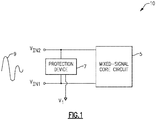
- FIG. 1 is a schematic block diagram of one example of a mixed-signal electronic system 10.
- the mixed-signal electronic system 10 includes a first pin or pad V IN1 , a second pin V IN2 , a mixed-signal core circuit 5, and a dual-tub junction-isolated voltage clamp device or protection device 7.
- the mixed-signal core circuit 5 includes a first input electrically connected to the first pin V IN1 and a second input electrically connected to the second pin V IN2 .
- the first and second pins V IN1 , V IN2 can correspond to pins of an integrated circuit on which the mixed-signal core circuit 5 is fabricated. In certain configurations, one or more of the first and second pins V IN1 , V IN2 can be used to transmit and/or receive signals to or from the mixed-signal core circuit 5.
- the transient electrical event 9 can correspond to, for example, an ESD and/or EOS event, such as those described by standards set by the Joint Electronic Device Engineering Council (JEDEC), the International Electrotechnical Commission (IEC), and/or the International Organization for Standardization (ISO).
- JEDEC Joint Electronic Device Engineering Council
- IEC International Electrotechnical Commission
- ISO International Organization for Standardization
- the mixed-signal core circuit 5 can be particularly susceptible to damage in configurations in which the mixed-signal core circuit 5 is implemented using low voltage circuitry.
- the first and second pins V IN1 , V IN2 are high voltage pins but operate with a relatively small voltage difference, and the mixed-signal core circuit 5 is implemented using low voltage circuitry electrically connected between the first and second pins V IN1 , V IN2 .
- the dual-tub junction-isolated voltage clamp device 7 includes a first terminal electrically connected to the first pin V IN1 , a second terminal electrically connected to the second pin V IN2 , and a bias terminal electrically connected to a first reference voltage V 1 , which can be, for example, a power low or ground supply.
- the first reference voltage V 1 can be used as a voltage reference to, for example, bias a substrate on which the dual-tub junction-isolated voltage clamp device 7 is fabricated.
- the dual-tub junction-isolated voltage clamp device 7 can be configured to provide fine-tuned forward and reverse protection characteristics between the first and second pins V IN1 , V IN2 .
- the dual-tub junction-isolated voltage clamp device 7 includes a dual-tub isolation structure including a p-type tub and an n-type tub. The p-type tub is electrically floating or unbiased and the n-type tub is electrically connected to the second pin V IN2 .
- Connecting the dual-tub junction-isolated voltage clamp device 7 in this manner can help prevent activation of parasitic PNP bipolar transistors structures associated with the semiconductor layout of the dual-tub junction-isolated voltage clamp device 7, even when a voltage difference between the first pin V IN1 and the first reference voltage V 1 and/or between the second pin V IN2 and the first reference voltage V 1 is relatively large, such as 60 V or more.
- the first and second pins V IN1 , V IN2 can correspond to signal pins, such as signal pins associated with a signaling interface.
- the first pin V IN1 is a signal pin and the second pin V IN2 is a high voltage power high supply pin, such as a power high supply pin configured to receive a supply voltage of 60 V or more.
- the second pin V IN2 is configured to have a higher operating voltage relative to the first pin V IN1 during normal operation of the mixed-signal electronic system 10.
- the mixed-signal electronic system 10 corresponds to a battery control circuit, such as a battery control circuit of an electric vehicle or automobile.
- a battery control circuit such as a battery control circuit of an electric vehicle or automobile.
- teachings herein are applicable to other configurations of electronic systems, such as electronic systems including an integrated circuit (IC) implemented using a bipolar CMOS DMOS (BCD) process.
- IC integrated circuit
- BCD bipolar CMOS DMOS
- a dual-tub junction-isolated voltage clamp device includes a PNPN or thyristor protection structure and a PN diode protection structure electrically connected in parallel between a first pin and a second pin.
- the PNPN protection structure is disposed in a p-well, and the PN diode protection structure is disposed in an n-well that is positioned adjacent the p-well.
- the PNPN protection structure includes a cathode electrically connected to the first pin and an anode and an anode-gate electrically connected to second pin
- the PN diode protection structure includes an anode electrically connected to the first pin and a cathode electrically connected to the second pin.
- the voltage clamp device further includes a p-type isolation region or tub configured to surround the sides and bottom of the p-well and the n-well, and an n-type isolation region or tub configured to surround the sides and bottom of the p-type tub.
- the p-type tub is configured to be electrically floating and the n-type tub is electrically connected to the second pin so as to provide the voltage clamp device with enhanced electrical isolation from a p-type substrate.
- the dual-tub isolation structure can prevent the n-well and/or p-well and the structures therein from interacting with external components and circuitry.
- the dual-tub isolation structure disconnects a collector of a parasitic PNP bipolar transistor associated with the p-type substrate, the n-type tub, and the p-type tub, and thus can increase substrate isolation and enhance IC latch-up immunity.
- the p-well corresponds to a high voltage p-well (HVPW)
- the PNPN protection structure includes a shallow p-well (SHPW), a shallow n-well (SHNW), a first n-type active (N+) region, a second N+ region, and a first p-type active (P+) fabricated within the HVPW.
- the SHPW is positioned adjacent the SHNW in the HVPW.
- the second N+ region is positioned in the SHPW and connected to the first pin, and the first N+ region and the first P+ region can be positioned adjacent one another in the SHNW and is connected to the second pin.
- the n-well corresponds to a high voltage n-well (HVNW) that is configured to laterally surround the HVPW
- the PN diode protection structure is provided using one or more SHNW/SHPW semiconductor junctions in the HVNW.
- the PNPN protection structure and the PN diode protection structure can be tuned by, for example, controlling spacing and geometry and/or including additional implants or structures, to provide forward and/or reverse trigger and holding voltages desirable for a particular application.
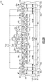
- Figure 2A a top plan view of a dual-tub junction-isolated voltage clamp device 80 or protection device 80 according to one embodiment.
- Figure 2B is a cross section of the dual-tub junction-isolated voltage clamp device 80 of Figure 2A taken along the lines 2B-2B.
- Figure 2C is an annotated cross section of the dual-tub junction-isolated voltage clamp device 80 of Figure 2A taken along the lines 2B-2B.
- the dual-tub junction-isolated voltage clamp device 80 includes a p-type substrate (P-SUB) 81, a p-type epitaxial layer (P-EPI) 91, a first high voltage p-well (HVPW) 82a, a second HVPW 82b, a third HVPW 82c, a fourth HVPW 82d, a first high voltage n-well (HVNW) 84a, a second HVNW 84b, a third HVNW 84c, a first shallow p-well (SHPW) 92a, a second SHPW 92b, a third SHPW 92c, a first shallow n-well (SHNW) 94a, a second SHNW 94b, a third SHNW 94c, first to eighth p-type active (P+) regions 83a-83h, first to ninth n-type active (N+) regions 85a-85i, an n
- the P-SUB 81, the first to sixth gate dielectric regions 86a-86f, the oxide regions 88, the n-type buried layer 89, the P-EPI 91, the first to third SHPWs 92a-92c, the deep p-well layer 93, and the first to third SHNWs 94a-94c, have been omitted from the top plan view of Figure 2A .
- the NBL 89 is disposed in the P-SUB 81, and the P-EPI 91 is disposed over the P-SUB 81. Additionally, the DPW 93 is positioned in the P-EPI 91 over the NBL 89.
- the P-EPI 91 is a lightly doped region allowing the operation at relatively high voltage conditions, such as in mixed-signal high voltage BCD processes. Additionally, in the illustrated configuration the first to fourth HVPWs 82a-82d and the first to third HVNWs 84a-84c are in the P-EPI 91 and configured as annular rings.
- the first HVNW 84a is configured to laterally surround the first HVPW 82a
- the second HVPW 82b is configured to laterally surround the first HVNW 84a
- the second HVNW 84b is configured to laterally surround the second HVPW 82b
- the third HVPW 82c is configured to laterally surround the second HVNW 84b
- the third HVNW 84c is configured to laterally surround the third HVPW 82c
- the fourth HVPW 82d is configured to laterally surround the third HVNW 84c.
- the first SHNW 94a and the first and second SHPWs 92a, 92b are disposed in the first HVPW 82a with the first SHNW 94a positioned between the first and second SHPWs 92a, 92b.
- the second SHNW 94b, the third SHPW 92c, and the third SHNW 94c have been configured as annular rings in the first HVNW 84a.
- the third SHPW 92c can be configured to laterally surround the second SHNW 94b
- the third SHNW 94c can be configured to laterally surround the third SHPW 92c.
- the first and second P+ regions 83a, 83b and the first N+ region 85a are disposed in the first SHNW 94a with the first N+ region 85a positioned between the first and second P+ regions 83a, 83b.
- the seventh N+ region 85g is disposed in the first SHNW 94a on a side of the first P+ region 83a opposite the first N+ region 85a.
- the eighth N+ region 85h is disposed in the first SHNW 94a on a side of the second P+ region 83b opposite the first N+ region 85a.
- the second N+ region 85b is disposed in the first SHPW 92a
- the third N+ region 85c is disposed in the second SHPW 92b.
- the sixth P+ region 83f extends along an edge between the first SHPW 92a and the first SHNW 94a and includes a first portion in the first SHPW 92a and a second portion in the first SHNW 94a.
- the seventh P+ region 83g extends along an edge between the second SHPW 92b and the first SHNW 94a and includes a first portion in the second SHPW 92b and a second portion in the first SHNW 94a.
- the fourth N+ region 85d is disposed in the second SHNW 94b, the third P+ region 83c is disposed in the third SHPW 92c, and the fifth N+ region 85e is disposed in the third SHNW 94c. Additionally, the fourth P+ region 83d is disposed in the second HVPW 82b, the sixth N+ region 85f is disposed in the second HVNW 84b, the fifth P+ region 83e is disposed in the third HVPW 82c, the ninth N+ region 85i is disposed in the third HVNW 84c, and the eighth P+ region 83h is disposed in the fourth HVPW 82d.
- the regions 82b and 93 co-operate to form a P-type tub, and regions 84b and 89 co-operate to form an N-type tub.
- the dual-tub junction-isolated voltage clamp device 80 includes the first to sixth gate dielectric regions 86a-86f and first to sixth gate conductors 87a-87f, which collective operate as gate structures that can provide implant blocking to define the position of certain diffusion or active regions.
- the first gate dielectric region 86a and the first gate conductor 87a extend over a portion of the first SHNW 94a between the first P+ region 83a and the seventh N+ region 85g.
- the second gate dielectric region 86b and the second gate conductor 87b extend over a portion of the first SHNW 94a between the second P+ region 83b and the eighth N+ region 85h.
- the third gate dielectric region 86c and the third gate conductor 87c extend over a portion of the first SHNW 94a between the sixth P+ region 83f and the seventh N+ region 85g.
- the fourth gate dielectric region 86d and the fourth gate conductor 87d extend over a portion of the first SHNW 94a between the seventh P+ region 83g and the eighth N+ region 85h.
- the fifth gate dielectric region 86e and the fifth gate conductor 87e extend over a portion of the first SHPW 92a between the sixth P+ region 83f and the second N+ region 85b.
- the sixth gate dielectric region 86f and the sixth gate conductor 87f extend over a portion of the second SHPW 92b between the seventh P+ region 83g and the third N+ region 85c.
- the first to sixth gate conductors 87a-87f include metal and/or polysilicon and the first to sixth gate dielectric regions 86a-86f include a dielectric such as a high-k dielectric.
- other configurations are possible.
- the illustrated dual-tub junction-isolated voltage clamp device 80 includes the oxide regions 88. Formation of the isolation regions can involve etching trenches in the P-EPI 91, filling the trenches with a dielectric, such as silicon dioxide (SiO 2 ), and removing the excess dielectric using any suitable method, such as chemical-mechanical planarization.
- the oxide regions 88 can be shallow trench regions disposed between certain active regions.
- the dual-tub junction-isolated voltage clamp device 80 can be fabricated using any suitable manufacturing process.
- the P-SUB 81 can be implanted with the NBL 89, and the P-EPI 91 can be grown over the P-SUB 81 and NBL 89 using an epitaxial growth process. Thereafter, the DPW 93 can be implanted in the P-EPI 91, and the first to fourth HVPWs 82a-82d and the first to third HVNWs 84a-84c can be implanted in the P-EPI 91.
- the first to third SHPWs 92a-92c and first to third SHNWs 94a-94c can be implanted, and the oxide regions 88 can be formed in the P-EPI 91.
- the first to sixth gate dielectric regions 86a-86f and the first to sixth gate conductors 87a-87f can be formed over the P-EPI 91, followed by implantation of the first to ninth N+ regions 85a-85i and the first to eighth P+ regions 83a-83h.
- the first to eighth P+ regions 83a-83h and the first to ninth N+ regions 85a-85i have a depth into the P-EPI 91 in the range of about 0.15 ⁇ m and about 0.5 ⁇ m, for example, about 0.2 ⁇ m
- the first to third SHPWs 92a-92c and the first to third SHNWs 94a-94c have a depth into the P-EPI 91 in the range of about 0.5 ⁇ m and about 1.5 ⁇ m, for example, about 1.0 ⁇ m
- the first to fourth HVPWs 82a-82d and the first to third HVNWs 84a-84c have a depth into the P-EPI 91 in the range of about 3.0 ⁇ m and about 4.5 ⁇ m, for example, about 3.5 ⁇ m.
- the P-EPI 91 can have a thickness in the range of about 4 ⁇ m and about 6 ⁇ m, for example, about 4.5 ⁇ m, and a peak doping of the NBL 89 can have a depth into the P-SUB 81 in the range of about 4.0 ⁇ m and about 5.5 ⁇ m, for example, about 5.0 ⁇ m.
- the first to fourth HVPWs 82a-82d can have a depth sufficient to reach the DPW 93
- the first to third HVNWs 84a-84c can have a depth sufficient to reach the NBL 89.
- the depth of peak doping of the DPW can be in the range of 1.5 ⁇ m to 3 ⁇ m, for example, 2.0 ⁇ m.
- the oxide regions 88 can be relatively deeper than the first to eighth P+ regions 83a-83h and the first to ninth N+ regions 85a-85i.
- the P-SUB 81 has a peak doping concentration in the range of about 0.5 x 10 15 atoms/cm -3 or cm -3 to about 1.5 x 10 15 cm -3 , for example, about 1.0 x 10 15 cm -3
- the P-EPI 91 has a peak doping concentration in the range of about 1 x 10 14 cm -3 to about 8.0 x 10 14 cm -3 , for example, about 2.0 x 10 14 cm -3 .
- the DPW 93 has a peak doping concentration in the range of about 8 x 10 16 cm -3 to about 2 x 10 17 cm -3 , for example, about 1.0 x 10 17 cm -3
- the NBL 89 has a peak doping concentration in the range of about 0.5 x 10 17 cm -3 to about 4 x 10 17 cm -3 , for example, about 2.5 x 10 17 cm -3 .
- the first to eighth P+ regions 83a-83h and the first to ninth N+ regions 85a-85i have a peak doping concentration in the range of about 1 x 10 20 cm -3 to about 8 x 10 20 cm -3 , for example, about 5 x 10 20 cm -3
- the SHPWs 92a-92c and the SHNWs 94a-94c have a peak doping concentration in the range of about 2.5 x 10 17 cm -3 to about 9.5 x 10 17 cm -3 , for example, about 7.0 x 10 17 cm -3
- the HVPWs 82a-82d and HVNWs 84a-84c have a peak doping concentration in the range of about 1.5 x 10 16 cm -3 to about 7.5 x 10 16 cm -3 , for example, about 3.0 x 10 16 cm -3 .
- the HVPWs 82a-82c can have a peak doping concentration that is less than a peak doping concentration of the SHPW 92, but a depth of the HVPWs 82a-82d can be greater than a depth of the SHPWs 92a-92c.
- the HVNWs 84a-84c can have a peak doping concentration that is less than a peak doping concentration of the SHNWs 94a-94c, but a depth of the HVNWs 84a-84c can be greater than a depth of the SHNWs 94a-94c.
- the first pin V IN1 is electrically connected to the third P+ region 83c and to the second and third N+ regions 85b, 85c.
- the second pin V IN2 is electrically connected to the first and second P+ regions 83a, 83b, to the first N+ region 85a, and to the fourth to sixth N+ regions 85d-85f.
- the first reference voltage V 1 is electrically connected to the fifth P+ active region 83e.
- the sixth P+ region 83f, the seventh P+ region 83g, the seventh N+ region 85g, the eighth N+ region 85h, and the first to sixth gate conductors 87a-87f are electrically floating or unconnected to a controlled electrical potential via metallization.
- the ninth N+ region 85i of Figure 2A can be electrically connected to a high voltage power high supply
- the eighth P+ region 83h of Figure 2A can be electrically connected to a high voltage power low supply.
- a voltage difference between the high voltage power high supply and the high voltage power low supply can be 60 V or more.
- the third HVNW 84c / ninth N+ region 85i and the fourth HVPW 82d / eighth P+ region 83h can operate as guard rings of the dual-tub junction-isolated voltage clamp device 80.
- electrically connecting the ninth N+ region 85i and the eighth P+ region 83h to high voltage power high and power low supplies, respectively, can provide enhanced isolation between the dual-tub junction-isolated voltage clamp device 80 and other circuitry fabricated in the P-SUB 81 and/or P-EPI 91.
- the dual-tub junction-isolated voltage clamp device 80 of Figure 2C has been annotated to show equivalent circuit devices of the illustrated structure, such as a first diode 21, a second diode 22, a third diode 23, a fourth diode 24, a first PNP parasitic bipolar transistor 31, a second PNP parasitic bipolar transistor 32, a third PNP parasitic bipolar transistor 33, an NPN thyristor bipolar transistor 41, a PNP thyristor bipolar transistor 42, and a thyristor resistor 43.
- various circuit devices have been illustrated for the left-hand side of the dual-tub junction-isolated voltage clamp device 80, the dual-tub junction-isolated voltage clamp device 80 can include corresponding circuit structures associated with the right-hand side of the device.
- the first diode 21 includes an anode associated with the third SHPW 92c and a cathode associated with the second SHNW 94b.
- the second diode 22 includes an anode associated with the third SHPW 92c and a cathode associated with the third SHNW 94c.
- the third diode 23 includes an anode associated with the third HVPW 82c / P-EPI 91 and a cathode associated with the second HVNW 84b.
- the fourth diode 24 includes an anode associated with the second HVPW 82b and a cathode associated with the third SHNW 94c.
- the first PNP parasitic bipolar transistor 31 includes an emitter associated with the third SHPW 92c, a base associated with the third SHNW 94c, and a collector associated with the second HVPW 82b.
- the second PNP parasitic bipolar transistor 32 includes an emitter associated with the third HVPW 82c / P-EPI 91, a base associated with the second HVNW 84b, and a collector associated with the second HVPW 82b.
- the third PNP parasitic bipolar transistor 33 includes an emitter associated with the P-SUB 81, a base associated with the NBL 89, and a collector associated with the second HVPW 82b / DPW 93.
- the NPN thyristor bipolar transistor 41 includes an emitter associated with the second N+ region 85b, a base associated with the first SHPW 92a, and a collector associated with the first SHNW 94a.
- the PNP thyristor bipolar transistor 42 includes an emitter associated with the first P+ region 83a, a base associated with the first SHNW 94a, and a collector associated with the first SHPW 92a.
- the thyristor resistor 43 is associated with the resistance of the first SHNW 94a / first N+ region 85a between the base and emitter of the PNP thyristor bipolar transistor 42.
- the second HVPW 82b and the DPW 93 operate as a p-type isolation region or tub that surrounds the bottom and sides of the first HVNW 84a and the first HVPW 82a and the structures and devices therein.
- the DPW 93 extends beneath the first HVNW 84a and the first HVPW 82a, while the first HVNW 84a contact the DPW 93 and surround the sides of the first HVNW 84a and the first HVPW 82a.
- the second HVNW 84b and the NBL 89 operate as an n-type isolation region or tub that surrounds the p-type tub.
- the NBL 89 extends beneath the DPW 93 and the second HVPW 82b, while the second HVNW 84b contacts the NBL 89 and surround the sides of the second HVPW 82b.
- the dual-tub isolation structure can electrically isolate the voltage clamp device 80 from other devices or structures fabricated in the P-SUB 81 and/or P-EPI 91. Additionally, as shown in Figures 2B-2C , the p-type tub can be electrically floating, and thus can be used to prevent the first to third PNP parasitic bipolar transistors 31-33 from activating, since the collectors of these transistors are electrically connected to the p-type tub.
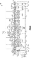
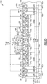
- FIG 3 is a circuit diagram 100 of the dual-tub junction-isolated voltage clamp device 80 of Figures 2A-2C .
- the circuit diagram 100 includes the first and second pins V IN1 , V IN2 , the first to fourth diodes 21-24, the first to third PNP parasitic bipolar transistors 31-33, the NPN thyristor bipolar transistor 41, the PNP thyristor bipolar transistor 42, and the thyristor resistor 43, which can be as described earlier.
- the first and second diodes 21, 22 operate as a PN diode protection structure 19, and the NPN thyristor bipolar transistor 41, the PNP thyristor bipolar transistor 42, and the thyristor resistor 43 operate as an SCR or thyristor or PNPN protection structure 20.
- the PN diode protection structure 19 and the PNPN protection structure 20 are electrically connected in parallel between the first and second pins V IN1 , V IN2 .
- the PN diode protection structure 19 includes an anode electrically connected to the first pin V IN1 and a cathode electrically connected to the second pin V IN2
- the PNPN protection structure 20 includes a cathode electrically connected to the first pin V IN1 and an anode electrically connected to the second pin V IN2
- the PNPN protection structure 20 further includes an anode-gate electrically connected to the second pin V IN2 through the thyristor resistor 43, and a cathode-gate. In the illustrated configuration, no resistor is provided between the cathode-gate and the cathode such that the NPN thyristor bipolar transistor 41 operates with a breakdown voltage collector-emitter base open (BVCEO) characteristic.
- BVCEO breakdown voltage collector-emitter base open
- circuit diagram 100 illustrates a particular configuration of circuit components
- persons having ordinary skill in the art will appreciate that the teachings herein are applicable to other configurations of protection structures and circuits.
- the PNPN protection structure 20 can be replaced with a different clamp voltage structure formation between the first and second pins V IN1 , V IN2 to achieve desired operating and/or clamp voltage targets, such as those described further below with reference to Figures 5A-7E .
- the first diode 21 includes an anode electrically connected to the first pin V IN1 and a cathode electrically connected to the second pin V IN2 .
- the second diode 22 includes an anode electrically connected to the first pin V IN1 and a cathode electrically connected to the second pin V IN2 .
- the third diode 23 includes an anode electrically connected to the first reference voltage V 1 and a cathode electrically connected to the second pin V IN2 .
- the fourth diode 24 includes a cathode electrically connected to the second pin V IN2 and an anode electrically connected to a collector of the first PNP parasitic bipolar transistor 31, to a collector of the second PNP parasitic bipolar transistor 32, and to a collector of the third PNP parasitic bipolar transistor 33.
- the first PNP parasitic bipolar transistor 31 further includes an emitter electrically connected to the first pin V IN1 and a base electrically connected to the second pin V IN2 .
- the second PNP parasitic bipolar transistor 32 further includes an emitter electrically connected to the first reference voltage V 1 and a base electrically connected to the second pin V IN2 .
- the third PNP parasitic bipolar transistor 33 further includes an emitter electrically connected to the first reference voltage V 1 and a base electrically connected to the second pin V IN2 .
- the PN diode protection structure 19 can be used to provide protection against a transient electrical event that increases the voltage of the first pin V IN1 relative to the voltage of the second pin V IN2 .
- the first and second diodes 21, 22 can activate and provide a low impedance path when the voltage difference between the first pin V IN1 and the second pin V IN2 is about equal to an activation voltage of the first and second diodes 21, 22.
- a voltage clamp such as the PNPN protection structure 20 can directly provide a reverse conduction path from V IN1 to V IN2 .
- the PNPN protection structure 20 can be used to provide protection against a transient electrical event that increases the voltage of the second pin V IN2 relative to the voltage of the first pin V IN1 .
- the NPN thyristor bipolar transistor 41 and the PNP thyristor bipolar transistor 42 are cross-coupled in feedback such that an increase in the collector current of the NPN thyristor bipolar transistor 41 increases the base current of the PNP thyristor bipolar transistor 42 and an increase in the collector current of the PNP thyristor bipolar transistor 42 increases the base current of the NPN thyristor bipolar transistor 41.
- the feedback between the NPN thyristor bipolar transistor 41 and the PNP thyristor bipolar transistor 42 can be regenerative and cause the PNPN protection structure 20 to enter a low-impedance state. Thereafter, the feedback between the transistors can maintain the PNPN protection structure 20 in the low-impedance state as long as the voltage difference between the second pin V IN2 and the first pin V IN1 exceeds a forward holding voltage of the PNPN protection structure 20.
- the protection characteristics of the dual-tub junction-isolated voltage clamp device 80 can be tuned by controlling the characteristics of structures corresponding to the PN diode protection structure 19 and/or the PNPN protection structure 20.
- the voltage clamp device can be configured to have a protection characteristic suitable for a particular application or operating conditions, such as those associated with operating current or voltage levels and/or a particular external noise disturbance environment.
- the voltage clamp device's reverse protection characteristic is based on an activation voltage of diode structures associated with SHPW/SHNW semiconductor junctions, such as a junction between the third SHPW 92c and the second SHNW 94b and a junction between the third SHPW 92c and the third SHNW 94c.
- the size, shaping, or other structural features of these regions can be controlled to provide a reverse protection characteristic that is desired for a particular application.
- other configurations of PN diode protection structures are possible.
- the voltage clamp device's forward protection characteristic is based on the forward trigger and holding voltages of the SCR or PNPN protection structure associated with the P+ regions 83a/83b, the SHNW 94a, the SHPWs 92a/92b, and the N+ regions 85a-85c.
- the size, shaping, or other structural features of these regions can be controlled to help achieve a forward protection characteristic that is desired for a particular application.
- other configurations of PN diode protection structures are possible and/or additional structures can be provided to further control the protection characteristic.
- the sixth and seventh P+ regions 83f, 83g and the seventh and eighth N+ regions 85g, 85h have been included in the voltage clamp device 80.
- the sixth and seventh P+ regions 83f, 83g increase the concentration of holes in the first and second SHPWs 92a, 92b, thereby lowering the device's blocking voltage and trigger voltage from the second pin V IN2 to the first pin V IN1 .
- the seventh and eighth N+ regions 85g, 85h increase the concentration of electrons in the first SHNW 94a and can eliminate a parasitic PMOS leakage path formation between the sixth and seventh P+ regions 83f, 83g and the first and second P+ regions 83a, 83b.
- Configuring the voltage clamp device 80 in this manner can provide lower breakdown defined by the higher doping concentration of P+ regions 83f, 83g and provide lower leakage as compared with a configuration in which the seventh and eighth N+ regions 85g, 85h are omitted.
- Figures 2A-2C illustrates one configuration of a PNPN protection structure, other configurations can be used.
- the voltage clamp device 80 includes a dual-tub isolation structure that prevents the voltage clamp device 80 from interacting with external components and circuitry fabricated in a common substrate with the voltage clamp device 80, thereby providing superior latch-up immunity.
- the collectors of the first to third PNP parasitic bipolar transistors 31-33 are electrically connected to the p-type tub, which has been configured to be electrically floating.
- the dual-tub isolation prevents activation of parasitic PNP bipolar structures and reduces the amount of charge the voltage clamp device 80 injects into the substrate during a transient electrical event received between the first and second pins V IN1 , V IN2 .
- the PNPN protection structure 20 and PN diode protection structure 19 provide forward and reverse voltage clamping, respectively, between the first and second pins V IN1 , V IN2 .
- the PNPN protection structure 20 provides a first blocking voltage between the first and second pins V IN1 , V IN2 , and the first blocking voltage is selected to be less than a junction isolation breakdown of the dual-tub isolation structure.
- the first and second pins V IN1 , V IN2 operate with voltages below the junction isolation breakdown voltage. Configuring the device is this manner allows the dual-tub isolation structure to provide the device with junction-isolation from a common substrate.
- the second pin V IN2 operates with a voltage greater than the first pin V IN1 and a voltage difference between the first and second pins V IN1 , V IN2 is less than the first blocking voltage.
- n-type tub refers to any suitable n-type tub, including, for example, those used in buried n-layer technologies or in deep n-well technologies.
- p-type tub refers to any suitable p-type tub.
- the dual-tub junction-isolated voltage clamp device 80 is fabricated in a P-EPI 91 layer formed over a P-SUB 81.
- teachings herein are applicable to other substrate configurations and manufacturing processes.
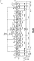
- Figure 4 is a cross section of another embodiment of a dual-tub junction-isolated voltage clamp device 110.
- the dual-tub junction-isolated voltage clamp device 110 of Figure 4 is similar to the dual-tub isolated voltage clamp device 80 of Figures 2A-2C , except that the dual-tub junction-isolated voltage clamp device 110 further includes a fourth SHPW 92d disposed in the second HVPW 82b.
- the fourth SHPW 92d can operate to reduce the gain of the first to third PNP parasitic bipolar transistors 31-33 shown in Figure 4 .
- the fourth SHPW 92d can be used to further reduce the likelihood of unintended activation of parasitic bipolar transistor structures.
- the fourth SHPW 92d can also impact the reverse breakdown voltage of the device, such as the reverse breakdown of the fourth diode 24 shown in Figure 2C .
- the voltage clamp device 110 of Figure 4 has been implemented such that the edges of the fourth SHPW 92d are spaced both from a boundary between the second HVPW 82b and the first HVNW 84a and from a boundary between the second HVPW 82b and the second HVNW 84b.
- the fourth SHPW 92d can be spaced from the second HVPW 82b / first HVNW 84a boundary and from the second HVPW 82b / second HVNW 84b boundary by a distance in the range of about 0.5 ⁇ m to about 3 ⁇ m, for example, about 1.5 ⁇ m. However, other distances are possible.
- Figure 5A is a cross section of another embodiment of a dual-tub junction-isolated voltage clamp device 120.
- the dual-tub junction-isolated voltage clamp device 120 of Figure 5A is similar to the dual-tub junction-isolated voltage clamp device 80 of Figures 2A-2C , except that the dual-tub junction-isolated voltage clamp device 120 illustrates a different configuration of a PNPN protection structure in which the sixth and seventh P+ regions 83f, 83g, the third to sixth gate dielectrics 86c-86f, and the third to sixth gate conductors 87c-87f have been omitted.
- the voltage clamp device 120 illustrates a configuration in which the seventh N+ region 85g is disposed along a boundary between the first SHPW 92a and the first SHNW 94a and in which the eighth N+ region 85h is disposed along a boundary between the second SHPW 92b and the first SHNW 94a.
- the voltage clamp device 120 of Figure 5A lacks P+ active regions in the first and second SHPWs 92a, 92b, and thus can have a holding voltage that is lower than and a trigger voltage that is lower than that of the voltage clamp device 80 of Figures 2A-2C .
- the voltage clamp device 80 of Figures 2A-2C can provide a forward trigger voltage during a 2ns rise time transmission line pulse (TLP) test in the range of about 10.8 V to about 13 V and a forward holding voltage in the range of about 2 V to about 2.1 V, while the voltage clamp device 120 of Figure 5A can provide a forward trigger voltage in the range of about 8.5 V to about 9.8V and a forward holding voltage in the range of about 1.5 V to about 1.8 V.
- TLP rise time transmission line pulse
- Figure 5B is a cross section of another embodiment of a dual-tub junction-isolated voltage clamp device 130.
- the dual-tub junction-isolated voltage clamp device 130 of Figure 5B is similar to the dual-tub junction-isolated voltage clamp device 80 of Figures 2A-2C , except that that the dual-tub junction-isolated voltage clamp device 130 illustrates a different configuration of a PNPN protection structure in which the sixth and seventh P+ regions 83f, 83g, the seventh and eighth N+ regions 85g, 85h, the first to sixth gate dielectrics 86c-86f, and the first to sixth gate conductors 87c-87fhave been omitted.
- the voltage clamp device 130 of Figure 5B can have a lower concentration of holes in the first and second SHPWs 92a, 92b and a lower concentration of electrons in the first SHNW 94a relative to the voltage clamp device 80 of Figures 2A-2C .
- the voltage clamp device 130 of Figure 5B can have a holding voltage that is higher than and a trigger voltage that is higher than that of the voltage clamp device 80 of Figures 2A-2C .
- the voltage clamp device 130 of Figure 5B can provide a forward trigger voltage in the range of about 15 V to about 18V and a forward holding voltage in the range of about 2.0 V to about 2.2 V.
- a forward trigger voltage in the range of about 15 V to about 18V
- a forward holding voltage in the range of about 2.0 V to about 2.2 V.
- Figure 5C is a cross section of another embodiment of a dual-tub junction-isolated voltage clamp device 140.
- the dual-tub junction-isolated voltage clamp device 140 of Figure 5C is similar to the dual-tub junction-isolated voltage clamp device 80 of Figures 2A-2C , except that the dual-tub junction-isolated voltage clamp device 140 illustrates a different configuration of a PNPN protection structure in which the sixth and seventh P+ regions 83f, 83g, the third to sixth gate dielectrics 86c-86f, and the third to sixth gate conductors 87c-87f have been omitted in favor of providing oxide regions 88 between the second N+ region 85b and the seventh N+ region 85g and between the third N+ region 85c and the eighth N+ region 85h.
- Configuring the voltage clamp device in this manner can result in the voltage clamp device 140 of Figure 5C having a holding voltage that is higher than and a trigger voltage that is higher than that of the voltage clamp device 80 of Figures 2A-2C .
- the voltage clamp device 140 of Figure 5C can provide a forward trigger voltage in the range of 15 V to about 18 V and a forward holding voltage in the range of about 2.5 V to about 4 V.
- trigger and holding voltages have been described, other configurations are possible.
- Figure 5D is a cross section of another embodiment of a dual-tub junction-isolated voltage clamp device 150.
- the dual-tub junction-isolated voltage clamp device 150 of Figure 5D is similar to the dual-tub junction-isolated voltage clamp device 80 of Figures 2A-2C , except that the dual-tub junction-isolated voltage clamp device 150 illustrates a different configuration of a PNPN protection structure in which a boundary between the first SHNW 94a and the first SHPW 92a is beneath the seventh N+ region 85g rather than beneath the sixth P+ region 83f, and in which a boundary between the first SHNW 94a and the second SHPW 92b is beneath the eighth N+ region 85h rather than beneath the seventh P+ region 83g.
- Configuring the voltage clamp device in this manner can result in the voltage clamp device 150 of Figure 5D having a holding voltage that is about the same level and a trigger voltage that is lower than that of the voltage clamp device 80 of Figures 2A-2C .
- the voltage clamp device 150 of Figure 5D can provide a forward trigger voltage in the range of about 8.5 V to about 9.8V and a forward holding voltage in the range of about 2.0 V to about 2.1 V.
- trigger and holding voltages have been described, other configurations are possible.
- Figure 6A is a schematic perspective view 170 of a portion of a dual-tub junction-isolated voltage clamp device according to one embodiment.
- Figure 6B is a schematic perspective view 175 of a portion of a dual-tub junction-isolated voltage clamp device according to another embodiment.
- the configuration shown in Figure 6A can correspond to a layout implementation of the first and second P+ regions 83a, 83b and the first N+ region 85a similar to that of the voltage clamp device 80 of Figures 2A-2C described earlier.
- the first N+ region 85a has been positioned between the first and second P+ regions 83a, 83b, and the first N+ region 85a and the first and second P+ regions 83a, 83b have been configured to extend substantially along a first direction.
- the configuration shown in Figure 6B includes a first P+ region 183a extending along the first direction, and a plurality of N+ island regions 185al-185a3 disposed in the first P+ region 183a and extending along the first direction.
- Configuring the voltage clamp device in this manner can provide fine-tuned control of the device's PNPN protection structure. For example, increasing the area of the P+ regions relative to the area of the N+ regions as shown in Figure 6B can operate to increase the strength of the PNP thyristor bipolar transistor 42 of Figure 2C relative to that of the NPN thyristor bipolar transistor 41 of Figure 2C .
- the geometric structure of certain regions can provide another degree of control to obtain a desired protection characteristic.
- the configuration of the geometric structure can be selected along with a particular thyristor protection configuration to achieve an overall protection characteristic.
- the configurations shown in Figures 6A-6B as well as other arrangement can be used in the combination with any of the voltage clamp devices described herein.
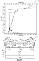
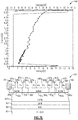
- FIGS 7A to 7E are schematic diagrams including transmission line pulse (TLP) data and partial cross sectional views for various embodiments of dual-tub junction-isolated voltage clamp devices.
- TLP transmission line pulse
- the TLP data corresponds to dual-tub junction-isolated voltage clamp devices developed in a 180 nm 1.8/5/60 V BCD process.
- the measurements were taken at about room temperature, and each TLP measurement point can correspond to a voltage and a current measurement obtained by forcing a rectangular 100 ns current pulse having about a 2ns rise time into the pad protection circuit and measuring the voltage of the pad protection circuit between about 40% and about 90 % of the current pulse width.
- the DC leakage measurements were taken at after each TLP current pulse. As skilled artisans will appreciate, a relatively small variation in the leakage current value after each pulse can indicate the integrity of the IC. In contrast, drastic change in the leakage current can indicate IC damage.
- Figure 7A includes TLP data 200 and a partial cross-section 201 of a dual-tub junction-isolated voltage clamp device similar to that of the voltage clamp device 120 of Figure 5A .
- the partial cross-section 201 corresponds to structures of the voltage clamp device related to the device's PNPN protection structure.
- the voltage clamp device includes other structures, such as a PN diode protection structure.
- the voltage clamp device can have a holding voltage of about 2 V and a trigger voltage between about 9 V and 9.5 V.
- a holding voltage of about 2 V
- a trigger voltage between about 9 V and 9.5 V.
- other values are possible, such as voltages that depend on geometric structural features and/or fabrication processes.
- Figure 7B includes TLP data 210 and a partial cross-section 211 of a dual-tub junction-isolated voltage clamp device.
- the voltage clamp device shown in the partial cross-section 211 includes a first SHNW 94a, first and second SHPWs 92a, 92b, first and second gate dielectric regions 86a, 86b, first and second gate conductor regions 87a, 87b, first second, sixth and seventh P+ regions 83a-83b, 83f-83g, first to third N+ regions 85a-85c, oxide regions 88, the first HVPW 82a, the DPW 93, the NBL 89, and the P-SUB 81.
- the NBL 89 is over the P-SUB 81
- the DPW 93 is over the NBL 89
- the first HVPW 82a is over the DPW 93.
- the first SHNW 94a and the first and second SHPWs 92a, 92b are in the first HVPW 82a, with the first SHNW 94a positioned between the first and second SHPWs 92a, 92b.
- the first N+ region 85a and the first and second P+ regions 83a, 83b are disposed in the first SHNW 94a with the first N+ region 85a between the first and second P+ regions 83a, 83b.
- the second N+ region 85b is disposed in the first SHPW 92a
- the third N+ region 85c is disposed in the second SHPW 92b
- the sixth P+ region 83f is disposed along a boundary between the first SHNW 94a and the first SHPW 92a
- the seventh P+ region 83g is disposed along a boundary between the first SHNW 94a and the second SHPW 92B.
- the first gate dielectric region 86a and the first gate conductor 87a are positioned over a portion of the first SHPW 92a between the second N+ region 85b and the sixth P+ region 83f.
- the second gate dielectric region 86b and the second gate conductor 87b are positioned over a portion of the second SHPW 92b between the third N+ region 85c and the seventh P+ region 83g.
- the voltage clamp device can have a holding voltage of about 2.1 V and a trigger voltage of about 11.2 V.
- a holding voltage of about 2.1 V
- a trigger voltage of about 11.2 V.
- other values are possible, such as voltages that depend on geometric structural features and/or fabrication processes.
- Figure 7C includes TLP data 220 and a partial cross-section 221 of a dual-tub junction-isolated voltage clamp device similar to that of the voltage clamp device 130 of Figure 5B .
- the voltage clamp device can have a holding voltage between about 2 V and 2.5 V and a trigger voltage of about 16.2 V.
- other values are possible, such as voltages that depend on geometric structural features and/or fabrication processes.
- Figure 7D includes TLP data 230 and a partial cross-section 231 of a dual-tub junction-isolated voltage clamp device similar.
- the partial cross-section 231 illustrates a PNPN protection structure similar to the PNPN protection structure of the voltage clamp device 80 of Figures 2A-2C , except that Figure 7D illustrates a configuration in which the fifth and sixth gate dielectric regions 86e, 86f and the fifth and sixth gate conductors 87e, 87f have been omitted in favor of using oxide regions 88.
- the voltage clamp device can have a holding voltage between about 2 V and 2.5 V and a trigger voltage between about 11 V and about 12 V.
- other values are possible, such as voltages that depend on geometric structural features and/or fabrication processes.
- Figure 7E includes TLP data 240 and a partial cross-section 241 of a dual-tub junction-isolated voltage clamp device similar to that of the voltage clamp device 80 of Figures 2A-2C .
- the voltage clamp device can have a holding voltage between about 2.1 V and a trigger voltage between about 11 V and about 12 V.
- the trigger and holding voltage of the configuration of Figure 7E are lower and the current handling capability is higher for a device of about the same dimensions.
- the difference in protection characteristics can be associated with the omission of oxide regions 88 between the second N+ region 85b and the sixth P+ region 83f and between the third N+ region 85c and the seventh P+ region 83g in favor of using gate structure 86e-86f, 87e-87f to separate these regions.
- FIGs 7D and 7E particular holding and trigger voltage data is shown in Figures 7D and 7E , other values are possible, such as voltages that depend on geometric structural features and/or fabrication processes.
- Figure 8 is another annotated cross section 300 of the dual-tub junction-isolated voltage clamp device 80 of Figures 2A-2C .
- the annotated cross section of Figure 8 is similar to the annotated cross section of Figure 2C , except that Figure 8 has been annotated to further include a first NPN parasitic bipolar transistor 301, a second NPN parasitic bipolar transistor 302, a first parasitic resistor 303, and a second parasitic resistor 304.
- the first NPN parasitic bipolar transistor 301 includes an emitter associated with the NBL 89, a base associated with the DPW 93, and a collector associated with the first HVNW 84a, and is a vertical bipolar transistor.
- the second NPN parasitic bipolar transistor 302 includes an emitter associated with the second HVNW 84b, a base associated with the second HVPW 82b, and a collector associated with the first HVNW 84a.
- the first parasitic resistor 303 is associated with the resistance of the first HVPW 82a / DPW 93 between the collector of the PNP thyristor bipolar transistor 42 and the bases of the first and second NPN parasitic bipolar transistors 301, 302.
- the second parasitic resistor 304 is associated with the resistance of the third SHPW 94c / first HVNW 84a between the cathode of the second diode 22 and the base of the first PNP parasitic bipolar transistor 301.
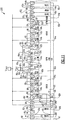
- Figure 9 is another circuit diagram 310 of the dual-tub junction-isolated voltage clamp device of Figures 2A-2C .
- the circuit diagram 310 of Figure 9 is similar to the circuit diagram 100 of Figure 3 , except that the circuit diagram 310 further includes the first and second NPN parasitic bipolar transistors 301, 302 and the first and second parasitic resistors 303, 304 described above with reference to Figure 8 .
- the first parasitic resistor 303 includes a first end electrically connected to the base of the NPN thyristor bipolar transistor 41 and to the collector of the PNP thyristor bipolar transistor 42. Additionally, the first parasitic resistor 303 further includes a second end electrically connected to the collectors of the first to third PNP parasitic bipolar transistors 31-33, to the anode of the fourth diode 24, and to the bases of the first and second NPN parasitic bipolar transistors 301, 302. Furthermore, as shown in Figure 9 , the collectors of the first and second NPN parasitic bipolar transistors 301, 302 are electrically connected to the second pin V IN2 through the second parasitic resistor 304. Additionally, the emitters of the first and second NPN parasitic bipolar transistors 301, 302 are electrically connected to the cathode of the third diode 23 and to the bases of the second and third PNP parasitic bipolar transistors 32, 33.
- the first and second NPN parasitic bipolar transistors 301, 302 can have a gain sufficient enough to impact the operation of a voltage clamp device in certain operating conditions.
- the first and second NPN parasitic bipolar transistors 301, 302 may have a relatively high common-emitter gain or beta ( ⁇ ) when the voltage clamp device is fabricated using a process in which the oxide regions 88 have a relatively shallow depth.
- the first PNP parasitic bipolar transistor 31 and the first and/or second NPN parasitic bipolar transistors 301, 302 may be undesirably activated during operation of the voltage clamp device.
- the activation of the first PNP parasitic bipolar transistor 31 and the first and/or second NPN parasitic bipolar transistors 301, 302 can be caused in part by forward biasing a path from the first pin V IN1 to the second pin V IN2 through the emitter-base junction of the PNP parasitic bipolar transistor 31 and to the collectors of the first and second NPN parasitic bipolar transistors 301, 302.
- the first and second NPN parasitic bipolar transistors 301, 302 can activate during operation, resulting of subsequent injection of residual substrate current through the parasitic substrate PNPs 32, 33.
- activation of the first and second NPN parasitic bipolar transistors 301, 302 can generate a flow of current into the bases of the second and third PNP parasitic bipolar transistors 32, 33, which can lead to a flow of current to the P-SUB 81.
- the increased substrate current can generate high power in semiconductor junctions between the n-type tub and the P-SUB 81 / P-EPI 91.
- Figure 10 is a top plan view of a dual-tub junction-isolated voltage clamp device 320 according to another embodiment.
- Figure 11 is a cross section of the dual-tub junction-isolated voltage clamp device 320 of Figure 10 taken along the lines 11-11.
- the voltage clamp device 320 of Figures 10 and 11 is similar to the voltage clamp device 80 of Figures 2A-2C , except that the voltage clamp device 320 further includes a fifth HVPW 82e, a fourth HVNW 82d, a ninth P+ region 83i, a tenth N+ region 85j, and a fourth SHPW 92d.
- the fifth HVPW 82e abuts and surrounds the second HVNW 84b.
- the fourth HVNW 82d abuts and surrounds the fifth HVPW 82e.
- the NBL 89 extends beneath the fifth HVPW 82e and the fourth HVNW 84d so as to electrically isolate the fifth HVPW 82e from the P-SUB 81.
- the third HVPW 82c surrounds but is spaced apart from the fourth HVNW 84d.
- the eighth P+ region 83i is disposed in the fifth HVPW 82e, and is electrically connected to the second pin V IN2 .
- the ninth N+ region 85j is disposed in the fourth HVNW 84d.
- the ninth N+ region 85j is electrically floating. Additionally, the fourth SHPW 92d is disposed in the second HVPW 82b, and in the illustrated configuration has a width that is about the same as a width of the second HVPW 82b.
- the fifth HVPW 82e operates as an embedded p-type guard well that surrounds the second HVNW 84b, which is associated with the device's n-type tub. Additionally, the fourth HVNW 84d operates as an embedded n-type collector guard well surrounding the fifth HVPW 82e.
- Including the fifth HVPW 82e and the fourth HVNW 84d can aid in reducing substrate current injection, such as current injected by the second and third PNP parasitic bipolar transistors 32, 33.
- the fifth HVPW 82e and the fourth HVNW 84d can operate to increase a base width of the second PNP bipolar transistor 32, thereby reducing the gain and current injection of the second PNP bipolar transistor 32.
- Figure 11 has been annotated to include the embedded PNP bipolar guard ring transistor 305, which can have an emitter associated with the second HVPW 82b, a base associated with the fourth HVNW 84d, and a collector associated with the fifth HVPW 82e.
- the base and collector of the embedded PNP bipolar guard ring transistor 305 can be electrically connected to the second pin V IN2 , while the emitter of the PNP lateral bipolar guard ring transistor 305 can be electrically connected to the collectors of the second and third PNP parasitic bipolar transistors 32, 33.
- the embedded PNP bipolar guard ring transistor 305 can operate to reduce in-situ the flow of current into the collectors of the second and third PNP parasitic bipolar transistors 32, 33, and thus can reduce the amount of current injected into the substrate.
- the PNP bipolar guard ring transistor 305 can also provide a current path between the first pin V IN1 and the second pin V IN2 , and thus can be used to encourage current flow confined within the isolation of the voltage clamp device 320.
- the voltage clamp device 320 also includes the fourth SHPW 92d, which can operate to decrease the gain of the second and third parasitic PNP bipolar transistors 32, 33.
- the widths of the second HVNW 84b, the fifth HVPW 82e, and/or the fourth HVNW 84d can be selected to be relatively large so as to decrease the gain of the second PNP parasitic bipolar transistor 32.
- a width of the second HVNW 84b is selected to be in the range of about 3.0 ⁇ m to about 6.0 ⁇ m, for instance, 5.5 ⁇ m
- a width of the fifth HVPW 82e is selected to be in the range of about 4.0 ⁇ m to about 8.0 ⁇ m, for instance, 6.0 ⁇ m
- a width of the fourth HVNW 84d is selected to be in the range of about 10 ⁇ m to about 40 ⁇ m, for instance 15 ⁇ m.
- Figure 12 is a cross section of another embodiment of a dual-tub junction-isolated voltage clamp device 330.
- the voltage clamp device 330 of Figure 12 is similar to the voltage clamp device 320 of Figure 11 , except that the voltage clamp device 330 illustrates a configuration in which the third SHPW 92c has been omitted, in which the fourth SHPW 92d has a narrower width than the second HVPW 82b, and in which the tenth N+ region 85j is electrically connected to the second pin V IN2 .
- Omitting the third SHPW 92c can aid in decreasing the gain of the first PNP parasitic bipolar transistor 31 by increasing the transistor's base width, thereby helping to prevent activation of the first PNP parasitic bipolar transistor 31 and the first and/or second NPN parasitic bipolar transistors 301, 302 shown in Figure 9 .
- the fourth SHPW 92d has been configured to have a width that is less than a width of the second HVPW 82b.
- the fourth SHPW 92d has a width that is 1 ⁇ m to 2 ⁇ m smaller than a width of the second HVPW 82b.
- Configuring the fourth SHPW 92d in this manner can help prevent the fourth SHPW 92d from significantly impacting the blocking voltage between the second HVPW 82b and the first and fourth HVNWs 84a, 84d.
- the fourth SHPW 92d can still help to decrease the gain of the second and third parasitic PNP bipolar transistors 32,33.
- the tenth N+ region 85j is electrically connected to the second pin V IN2 . Connecting the tenth N+ region 85j in this manner can increase the breakdown of the second and third PNP parasitic bipolar transistors 32, 33 and help mitigate the risk of the second and third PNP parasitic bipolar transistors 32, 33 from activating.
- Figure 12 illustrates a configuration in which the tenth N+ region 85j is electrically connected to the second pin V IN2
- the tenth N+ region 85j of the voltage clamp device 330 of Figure 12 can be electrically floating in a manner similar to that shown for the configuration of Figure 11 .
- Figure 11 illustrates a configuration in which the tenth N+ region 85j is electrically floating
- the tenth N+ region 85j of the voltage clamp device 320 of Figure 11 can be electrically connected to the second pin V IN2 .
- the protections devices can include layers, regions, and/or wells having n-type or p-type dopants.
- the doping types of all the layers, regions, and wells of the voltage clamp devices can be opposite to those described and shown in the above embodiments, and the same principles and advantages can still apply to the other embodiments.
- a complementary version of the voltage clamp device of Figures 2A-2C can be formed using an n-type substrate and n-type epitaxial layer and by reversing the doping polarity of the wells, active regions, and buried layers formed therein.
- complementary versions of the voltage clamp devices shown in Figures 4A-7E are also possible under the same principle described above.
- P-type regions can include a p-type semiconductor material, such as boron, as a dopant.
- n-type regions can include an n-type semiconductor material, such as phosphorous, as a dopant.
- Examples of the electronic devices can include, but are not limited to, consumer electronic products, parts of the consumer electronic products, electronic test equipment as well as high robustness industrial and automotive applications, among other applications in the semiconductor industry.
- Examples of the electronic devices can also include circuits of optical networks or other communication networks and circuits for voltage reference and electrical cars battery power management.
- the electronic products can include, power management integrated circuits for cell phones, base stations, a vehicle engine management controller, a transmission controller, etc. Further, the electronic device can include unfinished products, including those for industrial, medical and automotive applications.
Landscapes
- Semiconductor Integrated Circuits (AREA)
- Metal-Oxide And Bipolar Metal-Oxide Semiconductor Integrated Circuits (AREA)
Claims (20)
- Gerät zum Bereitstellen von Schutz vor transienten elektrischen Ereignissen, wobei das Gerät umfasst:ein erstes Terminal (VIN1);ein zweites Terminal (VIN2);einen ersten Quellenbereich vom p-Typ (82a);eine PNPN-Schutzstruktur (20), die in dem ersten Quellenbereich vom p-Typ angeordnet ist, wobei die PNPN-Schutzstruktur eine Anode, die elektrisch an das zweite Terminal angeschlossen ist, und eine Kathode, die elektrisch an das erste Terminal angeschlossen ist, einschließt;eine erste Quellenregion vom n-Typ (84a), die in dem ersten Quellenbereich vom p-Typ anliegt,eine PN-Diodenschutzstruktur, die in der ersten Quellenregion vom n-Typ angeordnet ist, wobei die PN-Diodenschutzstruktur (19) eine elektrisch an das erste Terminal angeschlossene Diode und eine elektrisch an das zweite Terminal angeschlossene Kathode einschließt;eine Wanne vom p-Typ (82b/93/82b), die konfiguriert ist, um die Seiten und den Boden der ersten Quellenregion vom p-Typ und die erste Quellenregion vom n-Typ zu umgeben;eine Wanne vom n-Typ (84b/89/84b), die konfiguriert ist, um die Seiten und den Boden des p-Typs zu umgeben; undein Substrat (81) vom p-Typ;wobei wenigstens ein Teil der Wanne vom n-Typ über dem Substrat vom p-Typ angeordnet ist, undwobei die Wanne vom p-Typ elektrisch floatet, undwobei die Wanne vom n-Typ elektrisch an das zweite Terminal angeschlossen ist.
- Gerät nach Anspruch 1,
weiterhin umfassend eine eingebettete Abschirmungsquelle vom p-Typ (82e), die die Wanne vom n-Typ umgibt und eine eingebettete Abschirmungsquelle vom n-Typ (84d), die die Abschirmungsquelle vom p-Typ umgibt, wobei die eingebettete Abschirmungsquelle vom p-Typ elektrisch an das zweite Terminal angeschlossen ist, wobei die Wanne vom n-Typ eine verborgene Schicht vom n-Typ umfasst, wobei die verborgene Schicht vom n-Typ (89) sich unterhalb der Abschirmungsquelle vom p-Typ und der eingebetteten Abschirmungsquelle vom n-Typ erstreckt. - Gerät nach Anspruch 2,
wobei mindestens Eines der Folgenden Anwendung findet:a) die eingebettete Abschirmungsquelle vom n-Typ (84d) ist elektrisch an das zweite Terminal angeschlossen;b) die Wanne vom p-Typ umfasst eine zweite Quellenregion vom p-Typ (82b) und eine flache Quelle vom p-Typ (92d), die in der zweiten Quellenregion vom p-Typ angeordnet ist, und optional ist eine Breite der flachen Quelle vom p-Typ geringer als eine Breite der zweiten Quellenregion vom p-Typ. - Gerät nach Anspruch 1 oder 2, weiterhin umfassend eine epitaktische Schicht vom p-Typ (91), die über dem Substrat vom p-Typ angeordnet ist, wobei die erste Quellenregion vom p-Typ und die erste Quellenregion vom n-Typ in der epitaktischen Schicht vom p-Typ angeordnet sind.
- Gerät nach Anspruch 4, wobei die Wanne vom n-Typ eine verborgene Schicht vom n-Typ (89), die in dem Substrat vom p-Typ angeordnet ist, und eine zweite Quellenregion vom n-Typ (84b), die in der epitaktischen Schicht vom p-Typ angeordnet ist, umfasst, wobei die zweite Quellenregion vom n-Typ elektrisch an das zweite Terminal angeschlossen ist.
- Gerät nach Anspruch 5, wobei die Wanne vom p-Typ eine zweite Quellenregion vom p-Typ (82b), die in der epitaktischen Schicht vom p-Typ angeordnet ist, und eine tiefe Quelle vom p-Typ (93), die in der epitaktischen Schicht von p-Typ angeordnet ist, umfasst, wobei die zweite Quellenregion vom p-Typ zwischen der ersten Quellenregion vom n-Typ und der zweiten Quellenregion vom n-Typ positioniert ist, und wobei ein Abschnitt der tiefen Quelle vom p-Typ zwischen der verborgenen Schicht vom n-Typ und der ersten Quellenregion vom n-Typ positioniert ist.
- Gerät nach Anspruch 1 oder 2, wobei wenigstens eines der Folgenden Anwendung findet:a) Die Wanne vom p-Typ umfasst weiterhin eine flache Quelle vom p-Typ (92d), die in einer zweiten Quellenregion vom p-Typ angeordnet ist, wobei die flache Quelle vom p-Typ von einer Grenze zwischen der zweiten Quellenregion vom p-Typ und der ersten Quellenregion vom n-Typ beabstandet ist und wobei die flache Quellenregion vom p-Typ von einer Grenze zwischen der zweiten Quellenregion vom p-Typ und der zweiten Quellenregion vom n-Typ beabstandet ist;b) die PNPN-Schutzstruktur umfasst weiterhin eine Anode-Gate-Region vom n-Typ (94a), wobei die Anode-Gate-Region vom n-Typ über einen Widerstand (43) elektrisch an das zweite Terminal angeschlossen ist.
- Gerät nach irgendeinem der voranstehenden Ansprüche, wobei die PNPN-Schutzstruktur umfasst:eine flache Quelle (92a) vom p-Typ, die in der ersten Quellenregion vom p-Typ angeordnet ist;eine flache Quelle vom n-Typ (94a), die in der ersten Quellenregion vom p-Typ angeordnet ist, die an der flachen Quelle vom p-Typ anliegt;eine erste aktive Region vom p-Typ (83a), die in der flachen Quelle vom n-Typ angeordnet ist, wobei die erste aktive Region vom p-Typ als die Anode der PNPN-Schutzstruktur arbeitet;eine erste aktive Region vom n-Typ (85a), die in der flachen Quelle vom n-Typ angeordnet ist, die an der ersten aktiven Region vom p-Typ anliegend ist, wobei die erste aktive Region vom p-Typ und die erste aktive Region vom n-Typ elektrisch an das zweite Terminal angeschlossen sind; undeine zweite aktive Region vom n-Typ (85b), die in der flachen Quelle vom p-Typ angeordnet ist, wobei die zweite aktive Region vom n-Typ als die Kathode der PNPN-Schutzstruktur arbeitet, wobei die zweite aktive Region vom n-Typ elektrisch an das erste Terminal angeschlossen ist.
- Gerät nach Anspruch 8, wobei die PNPN-Schutzstruktur weiterhin umfasst:eine dritte aktive Region vom n-Typ (85g), die entlang einer Grenze zwischen der flachen Quelle vom p-Typ und der flachen Quelle vom n-Typ angeordnet ist; undeine erste Gate-Struktur (87a), die an einem Abschnitt der flachen Quelle vom n-Typ zwischen der ersten aktiven Region vom p-Typ und der dritten aktiven Region vom n-Typ anliegend ist.
- Gerät nach Anspruch 9, wobei die PNPN-Schutzstruktur weiterhin umfasst:eine zweite aktive Region vom p-Typ (83f), die in der flachen Quelle vom p-Typ angeordnet ist, wobei die zweite aktive Region vom p-Typ zwischen der zweiten aktiven Region vom n-Typ und der dritten aktiven Region vom n-Typ positioniert ist;eine zweite Gate-Struktur (87c), die an einem Abschnitt der flachen Quelle vom p-Typ zwischen der zweiten aktiven Region vom p-Typ und der dritten aktiven Region vom n-Typ anliegend ist; undeine dritte Gate-Struktur (87e), die an einem Abschnitt der flachen Quelle vom p-Typ zwischen der zweiten aktiven Region vom p-Typ und der zweiten aktiven Region vom n-Typ anliegend ist.
- Gerät nach Anspruch 8, wobei die PNPN-Schutzstruktur weiterhin umfasst:eine dritte aktive Region vom n-Typ (85g), die in der flachen Quelle vom n-Typ angeordnet ist;eine erste Gate-Struktur (87a), die an einem Abschnitt der flachen Quelle vom n-Typ zwischen der ersten aktiven Region vom p-Typ und der dritten aktiven Region vom n-Typ anliegend ist.
- Gerät nach Anspruch 11, wobei die PNPN-Schutzstruktur weiterhin umfasst:eine zweite aktive Region vom p-Typ (83f), die entlang einer Grenze zwischen der flachen Quelle vom p-Typ und der flachen Quelle vom n-Typ angeordnet ist;eine zweite Gate-Struktur (87c), die anliegend an einem Abschnitt der flachen Quelle vom n-Typ zwischen der zweiten aktiven Region vom p-Typ und der dritten aktiven Region vom n-Typ anliegend ist; undeine dritte Gate-Struktur (87e), die an einem Abschnitt der flachen Quelle vom p-Typ zwischen der zweiten aktiven Region vom p-Typ und der zweiten aktiven Region vom n-Typ anliegend ist.
- Gerät nach Anspruch 9, 10, 11 oder 12, wobei die PNPN-Schutzstruktur weiterhin umfasst:
eine Oxidregion (88), die zwischen der dritten aktiven Region vom n-Typ und der zweiten aktiven Region vom n-Typ positioniert ist. - Gerät nach irgendeinem der Ansprüche 8 bis 13, wobei die erste aktive Region vom n-Typ eine Anoden-Gate-Region vom n-Typ (94a) umfasst, die erste mehrere Inselregionen vom n-Typ (185a1, 185a2) einschließt, die in der ersten aktiven Region vom p-Typ (183a) angeordnet ist, wobei die mehreren Inselregionen vom n-Typ sich entlang einer ersten Richtung erstrecken.
- Gerät nach irgendeinem der voranstehenden Ansprüche, wobei die PN-Diodenschutzstruktur umfasst:eine flache Quelle vom p-Typ (92c), die in der ersten Quellenregion vom n-Typ angeordnet ist;eine erste flache Quelle vom n-Typ (94b), die in der ersten Quellenregion vom n-Typ angeordnet ist, die an der flachen Quelle vom p-Typ anliegt, wobei die erste flache Quelle vom n-Typ zwischen der flachen Quelle vom p-Typ und der ersten Quellenregion vom p-Typ positioniert ist;eine erste aktive Region (83c) vom p-Typ, die in der flachen Quelle vom p-Typ angeordnet ist, wobei die erste aktive Region vom p-Typ (85d) elektrisch an das erste Terminal angeschlossen ist; undeine erste aktive Region vom n-Typ in der ersten flachen Quelle vom n-Typ angeordnet ist, wobei die erste aktive Region vom n-Typ elektrisch an das zweite Terminal angeschlossen ist.
- Gerät nach Anspruch 15, wobei die PN-Diodenschutzstruktur weiterhin umfasst:eine zweite flache Quelle vom n-Typ (94c), die in der ersten Quellenregion vom n-Typ angeordnet ist, die an einer Seite der flachen Quelle vom p-Typ gegenüber der ersten flachen Quelle vom n-Typ anliegt; undeine zweite aktive Region vom n-Typ (85e), die in der zweiten flachen Quelle vom n-Typ angeordnet ist, wobei die zweite aktive Region vom n-Typ elektrisch an das zweite Terminal angeschlossen ist.
- Gerät nach irgendeinem der voranstehenden Ansprüche, wobei die Doptypen des Substrats und alle Schichten, Regionen und Quelle denen gegenüberliegen, die in diesen Ansprüchen definiert sind.
- Verfahren zum Herstellen einer Schutzvorrichtung, wobei das Verfahren umfasst:Bereitstellen eines Substrats vom Typ p:Formen einer ersten Quellenregion vom p-Typ;Formen einer ersten Quellenregion vom n-Typ, die an der ersten Quellenregion vom p-Typ anliegt;Formen einer Wanne vom p-Typ, die die Seiten und den Boden der ersten Quellenregion vom p-Typ und die erste Quellenregion vom n-Typ umgibt;Formen einer Wanne vom n-Typ, die die Seiten und den Boden der Wanne vom p-Typ umgibt, wobei wenigstens ein Teil der Wanne vom n-Typ über einem Substrat vom p-Typ angeordnet ist;Formen einer PNPN-Schutzstruktur in der ersten Quellenregion vom p-Typ, wobei die PNPN-Schutzstruktur eine Kathode, die elektrisch an ein erstes Terminal angeschlossen ist, und eine Anode, die elektrisch an ein zweites Terminal angeschlossen ist, einschließt; undFormen einer PN-Diodenschutzstruktur in der ersten Quellenregion vom n-Typ, wobei die PN-Diodenschutzstruktur eine an das erste Terminal elektrisch angeschlossene Anode und eine an das zweite Terminal elektrisch angeschlossene Kathode einschließt;wobei wenigstens ein Teil der Wanne vom n-Typ über dem Substrat vom p-Typ angeordnet ist, undwobei die Wanne vom p-Typ elektrisch floatet, undwobei die Wanne vom n-Typ elektrisch an das zweite Terminal angeschlossen ist.
- Verfahren nach Anspruch 18, das weiterhin eine eingebettete Abschirmungsquelle vom p-Typ formt, die die Wanne vom n-Typ umgibt und eine eingebettete Abschirmungsquelle vom n-Typ formt, die die Abschirmungsquelle vom p-Typ umgibt, wobei die eingebettete Abschirmungsquelle vom p-Typ elektrisch an das zweite Terminal angeschlossen ist, wobei die Wanne vom n-Typ eine verborgene Schicht vom n-Typ umfasst, wobei die verborgene Schicht vom n-Typ sich unterhalb der eingebetteten Abschirmungsquelle vom p-Typ und der eingebetteten Abschirmungsquelle vom n-Typ erstreckt.
- Verfahren entweder nach Anspruch 18 oder nach Anspruch 19, wobei die Doptypen des Substrats und alle Schichten, Regionen und Quellen denen gegenüber sind; die in diesen Ansprüchen definiert sind.
Applications Claiming Priority (1)
| Application Number | Priority Date | Filing Date | Title |
|---|---|---|---|
| US13/896,123 US9147677B2 (en) | 2013-05-16 | 2013-05-16 | Dual-tub junction-isolated voltage clamp devices for protecting low voltage circuitry connected between high voltage interface pins and methods of forming the same |
Publications (2)
| Publication Number | Publication Date |
|---|---|
| EP2806462A1 EP2806462A1 (de) | 2014-11-26 |
| EP2806462B1 true EP2806462B1 (de) | 2019-02-27 |
Family
ID=50771051
Family Applications (1)
| Application Number | Title | Priority Date | Filing Date |
|---|---|---|---|
| EP14167969.6A Active EP2806462B1 (de) | 2013-05-16 | 2014-05-12 | Übergangsisolierte Doppelwannen-Spannungsschutzvorrichtung zum Schutz eines zwischen Hochspannungskontaktstiften angeschlossenen Niederspannungsschaltkreises und Verfahren zu deren Herstellung |
Country Status (3)
| Country | Link |
|---|---|
| US (1) | US9147677B2 (de) |
| EP (1) | EP2806462B1 (de) |
| CN (1) | CN104167414B (de) |
Cited By (1)
| Publication number | Priority date | Publication date | Assignee | Title |
|---|---|---|---|---|
| TWI716994B (zh) * | 2019-09-04 | 2021-01-21 | 張文宗 | 低觸發電壓靜電放電防護元件 |
Families Citing this family (58)
| Publication number | Priority date | Publication date | Assignee | Title |
|---|---|---|---|---|
| US9520486B2 (en) | 2009-11-04 | 2016-12-13 | Analog Devices, Inc. | Electrostatic protection device |
| US10199482B2 (en) | 2010-11-29 | 2019-02-05 | Analog Devices, Inc. | Apparatus for electrostatic discharge protection |
| US9025296B2 (en) * | 2011-01-06 | 2015-05-05 | Littelfuse, Inc. | Transient voltage suppressor |
| US9443754B2 (en) * | 2014-08-07 | 2016-09-13 | Macronix International Co., Ltd. | Semiconductor device including high-voltage diode |
| US9484739B2 (en) | 2014-09-25 | 2016-11-01 | Analog Devices Global | Overvoltage protection device and method |
| US9478608B2 (en) | 2014-11-18 | 2016-10-25 | Analog Devices, Inc. | Apparatus and methods for transceiver interface overvoltage clamping |
| US10068894B2 (en) | 2015-01-12 | 2018-09-04 | Analog Devices, Inc. | Low leakage bidirectional clamps and methods of forming the same |
| US9362266B1 (en) * | 2015-03-13 | 2016-06-07 | Taiwan Semiconductor Manufacturing Company Limited | Electrostatic discharge protection device for differential signal devices |
| US10181719B2 (en) | 2015-03-16 | 2019-01-15 | Analog Devices Global | Overvoltage blocking protection device |
| US9673187B2 (en) | 2015-04-07 | 2017-06-06 | Analog Devices, Inc. | High speed interface protection apparatus |
| US9899369B2 (en) * | 2015-09-22 | 2018-02-20 | United Microelectronics Corp. | Layout structure for electrostatic discharge protection |
| US10043793B2 (en) * | 2016-02-03 | 2018-08-07 | Taiwan Semiconductor Manufacturing Company Ltd. | Semiconductor device and circuit |
| US10158029B2 (en) | 2016-02-23 | 2018-12-18 | Analog Devices, Inc. | Apparatus and methods for robust overstress protection in compound semiconductor circuit applications |
| US10199369B2 (en) | 2016-03-04 | 2019-02-05 | Analog Devices, Inc. | Apparatus and methods for actively-controlled transient overstress protection with false condition shutdown |
| US9633993B1 (en) * | 2016-04-01 | 2017-04-25 | Texas Instruments Incorporated | Bipolar SCR |
| US9831233B2 (en) | 2016-04-29 | 2017-11-28 | Analog Devices Global | Apparatuses for communication systems transceiver interfaces |
| US10439024B2 (en) | 2016-06-13 | 2019-10-08 | Texas Instruments Incorporated | Integrated circuit with triple guard wall pocket isolation |
| US10177566B2 (en) | 2016-06-21 | 2019-01-08 | Analog Devices, Inc. | Apparatus and methods for actively-controlled trigger and latch release thyristor |
| US10734806B2 (en) | 2016-07-21 | 2020-08-04 | Analog Devices, Inc. | High voltage clamps with transient activation and activation release control |
| US9831134B1 (en) | 2016-09-28 | 2017-11-28 | Taiwan Semiconductor Manufacturing Co., Ltd. | Method of manufacturing a semiconductor device having deep wells |
| US10861845B2 (en) | 2016-12-06 | 2020-12-08 | Analog Devices, Inc. | Active interface resistance modulation switch |
| US10319714B2 (en) | 2017-01-24 | 2019-06-11 | Analog Devices, Inc. | Drain-extended metal-oxide-semiconductor bipolar switch for electrical overstress protection |
| US10404059B2 (en) | 2017-02-09 | 2019-09-03 | Analog Devices, Inc. | Distributed switches to suppress transient electrical overstress-induced latch-up |
| JP6678615B2 (ja) * | 2017-03-24 | 2020-04-08 | 株式会社東芝 | 半導体装置 |
| US10249609B2 (en) | 2017-08-10 | 2019-04-02 | Analog Devices, Inc. | Apparatuses for communication systems transceiver interfaces |
| US10950720B2 (en) * | 2017-10-23 | 2021-03-16 | Texas Instruments Incorporated | Electrostatic discharge guard ring with complementary drain extended devices |
| US10608431B2 (en) | 2017-10-26 | 2020-03-31 | Analog Devices, Inc. | Silicon controlled rectifier dynamic triggering and shutdown via control signal amplification |
| US10741543B2 (en) | 2017-11-30 | 2020-08-11 | Taiwan Semiconductor Manufacturing Co., Ltd. | Device including integrated electrostatic discharge protection component |
| TWI661530B (zh) * | 2018-02-13 | 2019-06-01 | 力晶積成電子製造股份有限公司 | 靜電放電保護元件 |
| KR102454469B1 (ko) * | 2018-04-17 | 2022-10-14 | 주식회사 디비하이텍 | Esd 보호용 scr 소자 |
| US10580856B2 (en) * | 2018-06-19 | 2020-03-03 | Nxp Usa, Inc. | Structure for improved noise signal isolation |
| TWI665802B (zh) * | 2018-08-08 | 2019-07-11 | 立錡科技股份有限公司 | 高壓元件及其製造方法 |
| US10581423B1 (en) | 2018-08-17 | 2020-03-03 | Analog Devices Global Unlimited Company | Fault tolerant low leakage switch |
| US10700056B2 (en) | 2018-09-07 | 2020-06-30 | Analog Devices, Inc. | Apparatus for automotive and communication systems transceiver interfaces |
| US11094690B2 (en) * | 2018-09-24 | 2021-08-17 | Board Of Trustees Of The University Of Arkansas | On-chip IEC ESD protection using parasitic PNP devices |
| US11387648B2 (en) | 2019-01-10 | 2022-07-12 | Analog Devices International Unlimited Company | Electrical overstress protection with low leakage current for high voltage tolerant high speed interfaces |
| US11004849B2 (en) | 2019-03-06 | 2021-05-11 | Analog Devices, Inc. | Distributed electrical overstress protection for large density and high data rate communication applications |
| DE102020111863B4 (de) | 2019-05-03 | 2026-02-05 | Analog Devices International Unlimited Company | Monolithisch integrierte Mikrowellenschaltung mit integriertem elektrischem Überlastungsschutz, Verfahren für elektrischen Überlastungsschutz in einer solchen und Halbleiterbaustein |
| US11469717B2 (en) | 2019-05-03 | 2022-10-11 | Analog Devices International Unlimited Company | Microwave amplifiers tolerant to electrical overstress |
| DE102019112036B4 (de) * | 2019-05-08 | 2023-10-12 | Elmos Semiconductor Se | Skalierbare ESD-Schutzstruktur mit einstellbarer Durchbruchspannung |
| US11342323B2 (en) * | 2019-05-30 | 2022-05-24 | Analog Devices, Inc. | High voltage tolerant circuit architecture for applications subject to electrical overstress fault conditions |
| US10971632B2 (en) * | 2019-06-24 | 2021-04-06 | Semiconductor Components Industries, Llc | High voltage diode on SOI substrate with trench-modified current path |
| KR102142156B1 (ko) * | 2019-07-18 | 2020-08-06 | 단국대학교 산학협력단 | 높은 홀딩 전압을 갖는 듀얼 구조의 정전기 방전 보호소자 |
| US12032014B2 (en) | 2019-09-09 | 2024-07-09 | Analog Devices International Unlimited Company | Semiconductor device configured for gate dielectric monitoring |
| DE102020123481A1 (de) | 2019-09-09 | 2021-03-11 | Analog Devices International Unlimited Company | Halbleitervorrichtung, die zur gate-dielektrikum-überwachung ausgebildet ist |
| US11362203B2 (en) | 2019-09-26 | 2022-06-14 | Analog Devices, Inc. | Electrical overstress protection for electronic systems subject to electromagnetic compatibility fault conditions |
| US11011510B2 (en) * | 2019-10-04 | 2021-05-18 | Texas Instruments Incorporated | Breakdown uniformity for ESD protection device |
| US11049853B2 (en) * | 2019-10-04 | 2021-06-29 | Texas Instruments Incorporated | ESD protection device with breakdown voltage stabilization |
| US11552190B2 (en) | 2019-12-12 | 2023-01-10 | Analog Devices International Unlimited Company | High voltage double-diffused metal oxide semiconductor transistor with isolated parasitic bipolar junction transistor region |
| US11595036B2 (en) | 2020-04-30 | 2023-02-28 | Analog Devices, Inc. | FinFET thyristors for protecting high-speed communication interfaces |
| CN114068523B (zh) * | 2021-11-18 | 2024-08-30 | 中国电子科技集团公司第五十八研究所 | 一种适用于高速存储器电路的esd静电保护结构 |
| US20240234409A1 (en) * | 2023-01-10 | 2024-07-11 | Globalfoundries U.S. Inc. | Structure including n-type well over n-type deep well and between pair of p-type wells for esd protection |
| KR20240133029A (ko) * | 2023-02-28 | 2024-09-04 | 주식회사 디비하이텍 | Esd 보호 소자 및 그 제조방법 |
| US12550453B2 (en) | 2023-04-25 | 2026-02-10 | Analog Devices, Inc. | Low capacitance poly-bounded silicon controlled rectifiers |
| US12543331B2 (en) * | 2023-04-26 | 2026-02-03 | Globalfoundries U.S. Inc. | Electrostatic discharge protection devices for bi-directional current protection |
| US20250098244A1 (en) * | 2023-09-15 | 2025-03-20 | Vanguard International Semiconductor Corporation | Electrostatic discharge (esd) protection device and transistor structure |
| US12477836B2 (en) | 2023-12-08 | 2025-11-18 | Analog Devices, Inc. | Low capacitance silicon controlled rectifier topology for overvoltage protection |
| CN119967834B (zh) * | 2025-01-21 | 2025-11-14 | 湖南静芯半导体科技有限公司 | 栅控增强型非对称双向可控硅静电防护器件及制作方法 |
Citations (2)
| Publication number | Priority date | Publication date | Assignee | Title |
|---|---|---|---|---|
| US5369041A (en) * | 1993-07-14 | 1994-11-29 | Texas Instruments Incorporated | Method for forming a silicon controlled rectifier |
| US20050269641A1 (en) * | 2004-06-04 | 2005-12-08 | Chun-Hsiang Lai | Electrostatic protection circuit |
Family Cites Families (109)
| Publication number | Priority date | Publication date | Assignee | Title |
|---|---|---|---|---|
| US3436667A (en) | 1964-12-08 | 1969-04-01 | Electric Associates Inc | Protection circuit for an amplifier system |
| US4626882A (en) | 1984-07-18 | 1986-12-02 | International Business Machines Corporation | Twin diode overvoltage protection structure |
| US4633283A (en) | 1985-03-11 | 1986-12-30 | Rca Corporation | Circuit and structure for protecting integrated circuits from destructive transient voltages |
| US5061652A (en) | 1990-01-23 | 1991-10-29 | International Business Machines Corporation | Method of manufacturing a semiconductor device structure employing a multi-level epitaxial structure |
| IT1253682B (it) | 1991-09-12 | 1995-08-22 | Sgs Thomson Microelectronics | Struttura di protezione dalle scariche elettrostatiche |
| US5276582A (en) | 1992-08-12 | 1994-01-04 | National Semiconductor Corporation | ESD protection using npn bipolar transistor |
| US5343053A (en) | 1993-05-21 | 1994-08-30 | David Sarnoff Research Center Inc. | SCR electrostatic discharge protection for integrated circuits |
| US5475335A (en) | 1994-04-01 | 1995-12-12 | National Semiconductor Corporation | High voltage cascaded charge pump |
| US5652689A (en) | 1994-08-29 | 1997-07-29 | United Microelectronics Corporation | ESD protection circuit located under protected bonding pad |
| JPH08139528A (ja) | 1994-09-14 | 1996-05-31 | Oki Electric Ind Co Ltd | トランジスタ保護回路 |
| FR2743938B1 (fr) | 1996-01-19 | 1998-04-10 | Sgs Thomson Microelectronics | Composant de protection d'interface de lignes telephoniques |
| TW299495B (en) | 1996-05-03 | 1997-03-01 | Winbond Electronics Corp | Electrostatic discharge protection circuit |
| US5663860A (en) | 1996-06-28 | 1997-09-02 | Harris Corporation | High voltage protection circuits |
| JP3601252B2 (ja) | 1996-09-13 | 2004-12-15 | 株式会社デンソー | ノックセンサ |
| KR100240872B1 (ko) | 1997-02-17 | 2000-01-15 | 윤종용 | 정전기 방전 보호 회로 및 그것을 구비하는 집적 회로 |
| US5889644A (en) | 1997-02-19 | 1999-03-30 | Micron Technology, Inc. | Device and method for electrostatic discharge protection of a circuit device |
| US6057184A (en) * | 1997-03-21 | 2000-05-02 | International Business Machines Corporation | Semiconductor device fabrication method using connecting implants |
| DE19721655C1 (de) | 1997-05-23 | 1998-12-03 | Daimler Benz Ag | Thyristor mit Selbstschutz |
| EP0915508A1 (de) * | 1997-10-10 | 1999-05-12 | STMicroelectronics S.r.l. | Integrierte Schaltung mit hocheffizienter Isolation durch PN-Übergang |
| US6137140A (en) | 1997-11-26 | 2000-10-24 | Texas Instruments Incorporated | Integrated SCR-LDMOS power device |
| US6365924B1 (en) | 1998-06-19 | 2002-04-02 | National Semiconductor Corporation | Dual direction over-voltage and over-current IC protection device and its cell structure |
| KR100307554B1 (ko) | 1998-06-30 | 2001-11-15 | 박종섭 | Esd 소자를 구비하는 반도체장치 |
| JP3244057B2 (ja) | 1998-07-16 | 2002-01-07 | 日本電気株式会社 | 基準電圧源回路 |
| US6236087B1 (en) | 1998-11-02 | 2001-05-22 | Analog Devices, Inc. | SCR cell for electrical overstress protection of electronic circuits |
| US6144542A (en) | 1998-12-15 | 2000-11-07 | Taiwan Semiconductor Manufacturing Co., Ltd. | ESD bus lines in CMOS IC's for whole-chip ESD protection |
| GB9907021D0 (en) | 1999-03-27 | 1999-05-19 | Koninkl Philips Electronics Nv | Switch circuit and semiconductor switch for battery-powered equipment |
| US6310379B1 (en) | 1999-06-03 | 2001-10-30 | Texas Instruments Incorporated | NMOS triggered NMOS ESD protection circuit using low voltage NMOS transistors |
| US6873505B2 (en) | 1999-09-14 | 2005-03-29 | United Microelectronics Corp. | Electrostatic discharge protective circuitry equipped with a common discharge line |
| US6512662B1 (en) | 1999-11-30 | 2003-01-28 | Illinois Institute Of Technology | Single structure all-direction ESD protection for integrated circuits |
| JP4065104B2 (ja) | 2000-12-25 | 2008-03-19 | 三洋電機株式会社 | 半導体集積回路装置およびその製造方法 |
| TW483143B (en) | 2001-02-05 | 2002-04-11 | Vanguard Int Semiconduct Corp | Voltage control device for electrostatic discharge protection and its related circuit |
| US6498357B2 (en) | 2001-02-09 | 2002-12-24 | United Microelectronics Corp. | Lateral SCR device for on-chip ESD protection in shallow-trench-isolation CMOS process |
| US6448123B1 (en) | 2001-02-20 | 2002-09-10 | Taiwan Semiconductor Manufacturing Company | Low capacitance ESD protection device |
| TW511269B (en) | 2001-03-05 | 2002-11-21 | Taiwan Semiconductor Mfg | Silicon-controlled rectifier device having deep well region structure and its application on electrostatic discharge protection circuit |
| US6768616B2 (en) | 2001-03-16 | 2004-07-27 | Sarnoff Corporation | Electrostatic discharge protection structures for high speed technologies with mixed and ultra-low voltage supplies |
| US6403992B1 (en) | 2001-06-05 | 2002-06-11 | Integrated Technology Express Inc. | Complementary metal-oxide semiconductor device |
| US7005708B2 (en) | 2001-06-14 | 2006-02-28 | Sarnoff Corporation | Minimum-dimension, fully-silicided MOS driver and ESD protection design for optimized inter-finger coupling |
| TW504828B (en) | 2001-08-17 | 2002-10-01 | Winbond Electronics Corp | Bi-directional electrical overstress and electrostatic discharge protection apparatus |
| US20030076636A1 (en) | 2001-10-23 | 2003-04-24 | Ming-Dou Ker | On-chip ESD protection circuit with a substrate-triggered SCR device |
| EP1453094A4 (de) | 2001-11-07 | 2006-08-23 | Shindengen Electric Mfg | Spitzenschutzhalbleiterbauelement |
| US6667870B1 (en) | 2001-12-12 | 2003-12-23 | Natiional Semiconductor Corporation | Fully distributed slave ESD clamps formed under the bond pads |
| US6704180B2 (en) | 2002-04-25 | 2004-03-09 | Medtronic, Inc. | Low input capacitance electrostatic discharge protection circuit utilizing feedback |
| US7179691B1 (en) | 2002-07-29 | 2007-02-20 | Taiwan Semiconductor Manufacturing Co., Ltd. | Method for four direction low capacitance ESD protection |
| US6724603B2 (en) | 2002-08-09 | 2004-04-20 | Motorola, Inc. | Electrostatic discharge protection circuitry and method of operation |
| JP4240983B2 (ja) | 2002-10-07 | 2009-03-18 | 沖電気工業株式会社 | 入力ピン容量の設定方法 |
| US6960811B2 (en) | 2002-11-07 | 2005-11-01 | Taiwan Semiconductor Manufacturing Co., Ltd. | Low capacitance ESD protection device, and integrated circuit including the same |
| US20040190208A1 (en) | 2003-03-26 | 2004-09-30 | Maxim Levit | Electrostatic discharge protection and methods thereof |
| US6909149B2 (en) | 2003-04-16 | 2005-06-21 | Sarnoff Corporation | Low voltage silicon controlled rectifier (SCR) for electrostatic discharge (ESD) protection of silicon-on-insulator technologies |
| US6756834B1 (en) | 2003-04-29 | 2004-06-29 | Pericom Semiconductor Corp. | Direct power-to-ground ESD protection with an electrostatic common-discharge line |
| US7196887B2 (en) | 2003-05-28 | 2007-03-27 | Texas Instruments Incorporated | PMOS electrostatic discharge (ESD) protection device |
| US7244992B2 (en) | 2003-07-17 | 2007-07-17 | Ming-Dou Ker | Turn-on-efficient bipolar structures with deep N-well for on-chip ESD protection |
| US6960792B1 (en) | 2003-09-30 | 2005-11-01 | National Semiconductor Corporation | Bi-directional silicon controlled rectifier structure with high holding voltage for latchup prevention |
| US7582938B2 (en) | 2003-10-01 | 2009-09-01 | Lsi Corporation | I/O and power ESD protection circuits by enhancing substrate-bias in deep-submicron CMOS process |
| US20050088794A1 (en) | 2003-10-23 | 2005-04-28 | International Business Machines Corporation | Removeable ESD for improving I/O pin bandwidth |
| US7038280B2 (en) | 2003-10-28 | 2006-05-02 | Analog Devices, Inc. | Integrated circuit bond pad structures and methods of making |
| US7067883B2 (en) | 2003-10-31 | 2006-06-27 | Lattice Semiconductor Corporation | Lateral high-voltage junction device |
| TWI223432B (en) | 2003-12-18 | 2004-11-01 | Univ Nat Chiao Tung | Double-triggered silicon controller rectifier and relevant circuitry |
| US7202114B2 (en) | 2004-01-13 | 2007-04-10 | Intersil Americas Inc. | On-chip structure for electrostatic discharge (ESD) protection |
| US7285458B2 (en) * | 2004-02-11 | 2007-10-23 | Chartered Semiconductor Manufacturing Ltd. | Method for forming an ESD protection circuit |
| CN100377321C (zh) | 2004-06-28 | 2008-03-26 | 中芯国际集成电路制造(上海)有限公司 | 用于高电压操作的金属氧化物半导体器件及其制造方法 |
| JP4282581B2 (ja) | 2004-09-29 | 2009-06-24 | 株式会社東芝 | 静電保護回路 |
| TWI237893B (en) | 2004-12-10 | 2005-08-11 | Richtek Technology Corp | Booster-type power management chip containing electrostatic discharge protection mechanism of output electrode |
| KR100627134B1 (ko) | 2004-12-14 | 2006-09-25 | 한국전자통신연구원 | 반도체 제어 정류기를 이용한 정전기 방전 보호 회로 |
| KR100638456B1 (ko) | 2004-12-30 | 2006-10-24 | 매그나칩 반도체 유한회사 | 이에스디 보호회로 및 그 제조방법 |
| US7285828B2 (en) * | 2005-01-12 | 2007-10-23 | Intersail Americas Inc. | Electrostatic discharge protection device for digital circuits and for applications with input/output bipolar voltage much higher than the core circuit power supply |
| US7414287B2 (en) | 2005-02-21 | 2008-08-19 | Texas Instruments Incorporated | System and method for making a LDMOS device with electrostatic discharge protection |
| DE102005013686A1 (de) | 2005-03-18 | 2006-10-05 | Atmel Germany Gmbh | ESD-Schutzschaltung mit skalierbarer Stromfestigkeit und Spannungsfestigkeit |
| US7232711B2 (en) | 2005-05-24 | 2007-06-19 | International Business Machines Corporation | Method and structure to prevent circuit network charging during fabrication of integrated circuits |
| US7566914B2 (en) | 2005-07-07 | 2009-07-28 | Intersil Americas Inc. | Devices with adjustable dual-polarity trigger- and holding-voltage/current for high level of electrostatic discharge protection in sub-micron mixed signal CMOS/BiCMOS integrated circuits |
| JP4995455B2 (ja) | 2005-11-30 | 2012-08-08 | ルネサスエレクトロニクス株式会社 | 半導体装置 |
| US7465995B2 (en) | 2006-01-10 | 2008-12-16 | Taiwan Semiconductor Manufacturing Co. | Resistor structure for ESD protection circuits |
| US7385793B1 (en) | 2006-01-24 | 2008-06-10 | Cypress Semiconductor Corporation | Cascode active shunt gate oxide project during electrostatic discharge event |
| US7345341B2 (en) | 2006-02-09 | 2008-03-18 | Taiwan Semiconductor Manufacturing Co., Ltd. | High voltage semiconductor devices and methods for fabricating the same |
| US7626243B2 (en) | 2006-08-04 | 2009-12-01 | Advanced Analogic Technologies, Inc. | ESD protection for bipolar-CMOS-DMOS integrated circuit devices |
| US20080029782A1 (en) | 2006-08-04 | 2008-02-07 | Texas Instruments, Inc. | Integrated ESD protection device |
| US7605431B2 (en) | 2006-09-20 | 2009-10-20 | Himax Technologies Limited | Electrostatic discharge protection apparatus for semiconductor devices |
| TWI370515B (en) | 2006-09-29 | 2012-08-11 | Megica Corp | Circuit component |
| US8431958B2 (en) | 2006-11-16 | 2013-04-30 | Alpha And Omega Semiconductor Ltd | Optimized configurations to integrate steering diodes in low capacitance transient voltage suppressor (TVS) |
| US7701012B2 (en) * | 2007-02-26 | 2010-04-20 | Freescale Semiconductor, Inc. | Complementary zener triggered bipolar ESD protection |
| TW200905860A (en) | 2007-07-31 | 2009-02-01 | Amazing Microelectroing Corp | Symmetric type bi-directional silicon control rectifier |
| US7834378B2 (en) | 2007-08-28 | 2010-11-16 | Fairchild Korea Semiconductor Ltd | SCR controlled by the power bias |
| DE102007040875B4 (de) | 2007-08-29 | 2017-11-16 | Austriamicrosystems Ag | Schaltungsanordnung zum Schutz vor elektrostatischen Entladungen und Verfahren zum Betreiben einer solchen |
| US7663190B2 (en) | 2007-10-08 | 2010-02-16 | Intersil Americas Inc. | Tunable voltage isolation ground to ground ESD clamp |
| JP2009194301A (ja) | 2008-02-18 | 2009-08-27 | Sanyo Electric Co Ltd | 半導体装置 |
| US7786504B2 (en) | 2008-03-20 | 2010-08-31 | Amazing Microelectronic Corp. | Bidirectional PNPN silicon-controlled rectifier |
| KR100976410B1 (ko) | 2008-05-28 | 2010-08-17 | 주식회사 하이닉스반도체 | 정전기 방전 장치 |
| US7868387B2 (en) | 2008-06-13 | 2011-01-11 | Analog Devices, Inc. | Low leakage protection device |
| KR20100003569A (ko) | 2008-07-01 | 2010-01-11 | 서경대학교 산학협력단 | 사이리스터를 이용한 esd 보호 회로 |
| US8198651B2 (en) | 2008-10-13 | 2012-06-12 | Infineon Technologies Ag | Electro static discharge protection device |
| JP2010129893A (ja) | 2008-11-28 | 2010-06-10 | Sony Corp | 半導体集積回路 |
| JP5172654B2 (ja) | 2008-12-27 | 2013-03-27 | 株式会社東芝 | 半導体装置 |
| US8222698B2 (en) | 2009-06-29 | 2012-07-17 | Analog Devices, Inc. | Bond pad with integrated transient over-voltage protection |
| US8044457B2 (en) | 2009-06-29 | 2011-10-25 | Analog Devices, Inc. | Transient over-voltage clamp |
| US9520486B2 (en) | 2009-11-04 | 2016-12-13 | Analog Devices, Inc. | Electrostatic protection device |
| US8648419B2 (en) | 2010-01-20 | 2014-02-11 | Freescale Semiconductor, Inc. | ESD protection device and method |
| US8952456B2 (en) * | 2010-02-24 | 2015-02-10 | Taiwan Semiconductor Manufacturing Co., Ltd. | Electrostatic discharge circuit using inductor-triggered silicon-controlled rectifier |
| US8432651B2 (en) | 2010-06-09 | 2013-04-30 | Analog Devices, Inc. | Apparatus and method for electronic systems reliability |
| US8665571B2 (en) | 2011-05-18 | 2014-03-04 | Analog Devices, Inc. | Apparatus and method for integrated circuit protection |
| US8368116B2 (en) | 2010-06-09 | 2013-02-05 | Analog Devices, Inc. | Apparatus and method for protecting electronic circuits |
| US8416543B2 (en) | 2010-07-08 | 2013-04-09 | Analog Devices, Inc. | Apparatus and method for electronic circuit protection |
| US8553380B2 (en) | 2010-07-08 | 2013-10-08 | Analog Devices, Inc. | Apparatus and method for electronic circuit protection |
| US8217461B1 (en) * | 2010-07-09 | 2012-07-10 | Altera Corporation | ESD protection circuit |
| US8466489B2 (en) | 2011-02-04 | 2013-06-18 | Analog Devices, Inc. | Apparatus and method for transient electrical overstress protection |
| US8592860B2 (en) | 2011-02-11 | 2013-11-26 | Analog Devices, Inc. | Apparatus and method for protection of electronic circuits operating under high stress conditions |
| US8476736B2 (en) * | 2011-02-18 | 2013-07-02 | Taiwan Semiconductor Manufacturing Company, Ltd. | Low leakage diodes |
| US8680620B2 (en) | 2011-08-04 | 2014-03-25 | Analog Devices, Inc. | Bi-directional blocking voltage protection devices and methods of forming the same |
| US8947841B2 (en) | 2012-02-13 | 2015-02-03 | Analog Devices, Inc. | Protection systems for integrated circuits and methods of forming the same |
| US8946822B2 (en) | 2012-03-19 | 2015-02-03 | Analog Devices, Inc. | Apparatus and method for protection of precision mixed-signal electronic circuits |
| US8796729B2 (en) * | 2012-11-20 | 2014-08-05 | Analog Devices, Inc. | Junction-isolated blocking voltage devices with integrated protection structures and methods of forming the same |
-
2013
- 2013-05-16 US US13/896,123 patent/US9147677B2/en active Active
-
2014
- 2014-05-12 EP EP14167969.6A patent/EP2806462B1/de active Active
- 2014-05-16 CN CN201410206744.9A patent/CN104167414B/zh active Active
Patent Citations (2)
| Publication number | Priority date | Publication date | Assignee | Title |
|---|---|---|---|---|
| US5369041A (en) * | 1993-07-14 | 1994-11-29 | Texas Instruments Incorporated | Method for forming a silicon controlled rectifier |
| US20050269641A1 (en) * | 2004-06-04 | 2005-12-08 | Chun-Hsiang Lai | Electrostatic protection circuit |
Cited By (2)
| Publication number | Priority date | Publication date | Assignee | Title |
|---|---|---|---|---|
| TWI716994B (zh) * | 2019-09-04 | 2021-01-21 | 張文宗 | 低觸發電壓靜電放電防護元件 |
| US11222886B2 (en) | 2019-09-04 | 2022-01-11 | Wen-Tsung Chang | ESD protection device with low trigger voltage |
Also Published As
| Publication number | Publication date |
|---|---|
| US9147677B2 (en) | 2015-09-29 |
| CN104167414B (zh) | 2017-04-12 |
| CN104167414A (zh) | 2014-11-26 |
| US20140339601A1 (en) | 2014-11-20 |
| EP2806462A1 (de) | 2014-11-26 |
Similar Documents
| Publication | Publication Date | Title |
|---|---|---|
| EP2806462B1 (de) | Übergangsisolierte Doppelwannen-Spannungsschutzvorrichtung zum Schutz eines zwischen Hochspannungskontaktstiften angeschlossenen Niederspannungsschaltkreises und Verfahren zu deren Herstellung | |
| US8796729B2 (en) | Junction-isolated blocking voltage devices with integrated protection structures and methods of forming the same | |
| US10068894B2 (en) | Low leakage bidirectional clamps and methods of forming the same | |
| US8835977B2 (en) | TVS with low capacitance and forward voltage drop with depleted SCR as steering diode | |
| US8338854B2 (en) | TVS with low capacitance and forward voltage drop with depleted SCR as steering diode | |
| US8610251B1 (en) | Low voltage protection devices for precision transceivers and methods of forming the same | |
| US9275991B2 (en) | Apparatus for transceiver signal isolation and voltage clamp | |
| US8466489B2 (en) | Apparatus and method for transient electrical overstress protection | |
| EP2442359B1 (de) | Flächeneffiziente Hochspannungs-Bipolar-ESD-Schutzvorrichtung | |
| US8637899B2 (en) | Method and apparatus for protection and high voltage isolation of low voltage communication interface terminals | |
| US8860080B2 (en) | Interface protection device with integrated supply clamp and method of forming the same | |
| US8680620B2 (en) | Bi-directional blocking voltage protection devices and methods of forming the same | |
| US9576945B2 (en) | Methods and apparatus for increased holding voltage in silicon controlled rectifiers for ESD protection | |
| KR101975608B1 (ko) | 고전압용 esd 트랜지스터 및 그 정전기 보호 회로 | |
| KR101847227B1 (ko) | Esd 트랜지스터 | |
| US10483257B2 (en) | Low voltage NPN with low trigger voltage and high snap back voltage for ESD protection | |
| US9614369B2 (en) | ESD protection device | |
| CN114649326A (zh) | 具有集成肖特基势垒的绝缘栅双极晶体管 | |
| US8982516B2 (en) | Area-efficient high voltage bipolar-based ESD protection targeting narrow design windows | |
| WO2017173444A1 (en) | Bipolar scr |
Legal Events
| Date | Code | Title | Description |
|---|---|---|---|
| PUAI | Public reference made under article 153(3) epc to a published international application that has entered the european phase |
Free format text: ORIGINAL CODE: 0009012 |
|
| 17P | Request for examination filed |
Effective date: 20140512 |
|
| AK | Designated contracting states |
Kind code of ref document: A1 Designated state(s): AL AT BE BG CH CY CZ DE DK EE ES FI FR GB GR HR HU IE IS IT LI LT LU LV MC MK MT NL NO PL PT RO RS SE SI SK SM TR |
|
| AX | Request for extension of the european patent |
Extension state: BA ME |
|
| R17P | Request for examination filed (corrected) |
Effective date: 20141218 |
|
| RBV | Designated contracting states (corrected) |
Designated state(s): AL AT BE BG CH CY CZ DE DK EE ES FI FR GB GR HR HU IE IS IT LI LT LU LV MC MK MT NL NO PL PT RO RS SE SI SK SM TR |
|
| RAP1 | Party data changed (applicant data changed or rights of an application transferred) |
Owner name: ANALOG DEVICES GLOBAL |
|
| 17Q | First examination report despatched |
Effective date: 20160927 |
|
| STAA | Information on the status of an ep patent application or granted ep patent |
Free format text: STATUS: EXAMINATION IS IN PROGRESS |
|
| RAP1 | Party data changed (applicant data changed or rights of an application transferred) |
Owner name: ANALOG DEVICES GLOBAL UNLIMITED COMPANY |
|
| REG | Reference to a national code |
Ref country code: DE Ref legal event code: R079 Ref document number: 602014041666 Country of ref document: DE Free format text: PREVIOUS MAIN CLASS: H01L0029740000 Ipc: H01L0029870000 |
|
| GRAP | Despatch of communication of intention to grant a patent |
Free format text: ORIGINAL CODE: EPIDOSNIGR1 |
|
| STAA | Information on the status of an ep patent application or granted ep patent |
Free format text: STATUS: GRANT OF PATENT IS INTENDED |
|
| RIC1 | Information provided on ipc code assigned before grant |
Ipc: H01L 27/02 20060101ALI20180828BHEP Ipc: H01L 29/87 20060101AFI20180828BHEP Ipc: H01L 27/08 20060101ALI20180828BHEP Ipc: H01L 29/10 20060101ALN20180828BHEP Ipc: H01L 21/8238 20060101ALN20180828BHEP Ipc: H01L 21/761 20060101ALN20180828BHEP |
|
| RIC1 | Information provided on ipc code assigned before grant |
Ipc: H01L 29/87 20060101AFI20180907BHEP Ipc: H01L 29/10 20060101ALN20180907BHEP Ipc: H01L 21/8238 20060101ALN20180907BHEP Ipc: H01L 27/08 20060101ALI20180907BHEP Ipc: H01L 21/761 20060101ALN20180907BHEP Ipc: H01L 27/02 20060101ALI20180907BHEP |
|
| INTG | Intention to grant announced |
Effective date: 20180925 |
|
| GRAS | Grant fee paid |
Free format text: ORIGINAL CODE: EPIDOSNIGR3 |
|
| GRAA | (expected) grant |
Free format text: ORIGINAL CODE: 0009210 |
|
| STAA | Information on the status of an ep patent application or granted ep patent |
Free format text: STATUS: THE PATENT HAS BEEN GRANTED |
|
| AK | Designated contracting states |
Kind code of ref document: B1 Designated state(s): AL AT BE BG CH CY CZ DE DK EE ES FI FR GB GR HR HU IE IS IT LI LT LU LV MC MK MT NL NO PL PT RO RS SE SI SK SM TR |
|
| REG | Reference to a national code |
Ref country code: GB Ref legal event code: FG4D |
|
| REG | Reference to a national code |
Ref country code: CH Ref legal event code: EP |
|
| REG | Reference to a national code |
Ref country code: AT Ref legal event code: REF Ref document number: 1102585 Country of ref document: AT Kind code of ref document: T Effective date: 20190315 |
|
| REG | Reference to a national code |
Ref country code: IE Ref legal event code: FG4D |
|
| REG | Reference to a national code |
Ref country code: DE Ref legal event code: R096 Ref document number: 602014041666 Country of ref document: DE |
|
| REG | Reference to a national code |
Ref country code: NL Ref legal event code: MP Effective date: 20190227 |
|
| REG | Reference to a national code |
Ref country code: LT Ref legal event code: MG4D |
|
| PG25 | Lapsed in a contracting state [announced via postgrant information from national office to epo] |
Ref country code: SE Free format text: LAPSE BECAUSE OF FAILURE TO SUBMIT A TRANSLATION OF THE DESCRIPTION OR TO PAY THE FEE WITHIN THE PRESCRIBED TIME-LIMIT Effective date: 20190227 Ref country code: NL Free format text: LAPSE BECAUSE OF FAILURE TO SUBMIT A TRANSLATION OF THE DESCRIPTION OR TO PAY THE FEE WITHIN THE PRESCRIBED TIME-LIMIT Effective date: 20190227 Ref country code: PT Free format text: LAPSE BECAUSE OF FAILURE TO SUBMIT A TRANSLATION OF THE DESCRIPTION OR TO PAY THE FEE WITHIN THE PRESCRIBED TIME-LIMIT Effective date: 20190627 Ref country code: LT Free format text: LAPSE BECAUSE OF FAILURE TO SUBMIT A TRANSLATION OF THE DESCRIPTION OR TO PAY THE FEE WITHIN THE PRESCRIBED TIME-LIMIT Effective date: 20190227 Ref country code: NO Free format text: LAPSE BECAUSE OF FAILURE TO SUBMIT A TRANSLATION OF THE DESCRIPTION OR TO PAY THE FEE WITHIN THE PRESCRIBED TIME-LIMIT Effective date: 20190527 Ref country code: FI Free format text: LAPSE BECAUSE OF FAILURE TO SUBMIT A TRANSLATION OF THE DESCRIPTION OR TO PAY THE FEE WITHIN THE PRESCRIBED TIME-LIMIT Effective date: 20190227 |
|
| PG25 | Lapsed in a contracting state [announced via postgrant information from national office to epo] |
Ref country code: IS Free format text: LAPSE BECAUSE OF FAILURE TO SUBMIT A TRANSLATION OF THE DESCRIPTION OR TO PAY THE FEE WITHIN THE PRESCRIBED TIME-LIMIT Effective date: 20190627 Ref country code: BG Free format text: LAPSE BECAUSE OF FAILURE TO SUBMIT A TRANSLATION OF THE DESCRIPTION OR TO PAY THE FEE WITHIN THE PRESCRIBED TIME-LIMIT Effective date: 20190527 Ref country code: RS Free format text: LAPSE BECAUSE OF FAILURE TO SUBMIT A TRANSLATION OF THE DESCRIPTION OR TO PAY THE FEE WITHIN THE PRESCRIBED TIME-LIMIT Effective date: 20190227 Ref country code: HR Free format text: LAPSE BECAUSE OF FAILURE TO SUBMIT A TRANSLATION OF THE DESCRIPTION OR TO PAY THE FEE WITHIN THE PRESCRIBED TIME-LIMIT Effective date: 20190227 Ref country code: LV Free format text: LAPSE BECAUSE OF FAILURE TO SUBMIT A TRANSLATION OF THE DESCRIPTION OR TO PAY THE FEE WITHIN THE PRESCRIBED TIME-LIMIT Effective date: 20190227 Ref country code: GR Free format text: LAPSE BECAUSE OF FAILURE TO SUBMIT A TRANSLATION OF THE DESCRIPTION OR TO PAY THE FEE WITHIN THE PRESCRIBED TIME-LIMIT Effective date: 20190528 |
|
| REG | Reference to a national code |
Ref country code: AT Ref legal event code: MK05 Ref document number: 1102585 Country of ref document: AT Kind code of ref document: T Effective date: 20190227 |
|
| PG25 | Lapsed in a contracting state [announced via postgrant information from national office to epo] |
Ref country code: CZ Free format text: LAPSE BECAUSE OF FAILURE TO SUBMIT A TRANSLATION OF THE DESCRIPTION OR TO PAY THE FEE WITHIN THE PRESCRIBED TIME-LIMIT Effective date: 20190227 Ref country code: IT Free format text: LAPSE BECAUSE OF FAILURE TO SUBMIT A TRANSLATION OF THE DESCRIPTION OR TO PAY THE FEE WITHIN THE PRESCRIBED TIME-LIMIT Effective date: 20190227 Ref country code: SK Free format text: LAPSE BECAUSE OF FAILURE TO SUBMIT A TRANSLATION OF THE DESCRIPTION OR TO PAY THE FEE WITHIN THE PRESCRIBED TIME-LIMIT Effective date: 20190227 Ref country code: AL Free format text: LAPSE BECAUSE OF FAILURE TO SUBMIT A TRANSLATION OF THE DESCRIPTION OR TO PAY THE FEE WITHIN THE PRESCRIBED TIME-LIMIT Effective date: 20190227 Ref country code: EE Free format text: LAPSE BECAUSE OF FAILURE TO SUBMIT A TRANSLATION OF THE DESCRIPTION OR TO PAY THE FEE WITHIN THE PRESCRIBED TIME-LIMIT Effective date: 20190227 Ref country code: DK Free format text: LAPSE BECAUSE OF FAILURE TO SUBMIT A TRANSLATION OF THE DESCRIPTION OR TO PAY THE FEE WITHIN THE PRESCRIBED TIME-LIMIT Effective date: 20190227 Ref country code: ES Free format text: LAPSE BECAUSE OF FAILURE TO SUBMIT A TRANSLATION OF THE DESCRIPTION OR TO PAY THE FEE WITHIN THE PRESCRIBED TIME-LIMIT Effective date: 20190227 Ref country code: RO Free format text: LAPSE BECAUSE OF FAILURE TO SUBMIT A TRANSLATION OF THE DESCRIPTION OR TO PAY THE FEE WITHIN THE PRESCRIBED TIME-LIMIT Effective date: 20190227 |
|
| REG | Reference to a national code |
Ref country code: DE Ref legal event code: R097 Ref document number: 602014041666 Country of ref document: DE |
|
| PG25 | Lapsed in a contracting state [announced via postgrant information from national office to epo] |
Ref country code: SM Free format text: LAPSE BECAUSE OF FAILURE TO SUBMIT A TRANSLATION OF THE DESCRIPTION OR TO PAY THE FEE WITHIN THE PRESCRIBED TIME-LIMIT Effective date: 20190227 Ref country code: PL Free format text: LAPSE BECAUSE OF FAILURE TO SUBMIT A TRANSLATION OF THE DESCRIPTION OR TO PAY THE FEE WITHIN THE PRESCRIBED TIME-LIMIT Effective date: 20190227 |
|
| REG | Reference to a national code |
Ref country code: CH Ref legal event code: PL |
|
| PG25 | Lapsed in a contracting state [announced via postgrant information from national office to epo] |
Ref country code: AT Free format text: LAPSE BECAUSE OF FAILURE TO SUBMIT A TRANSLATION OF THE DESCRIPTION OR TO PAY THE FEE WITHIN THE PRESCRIBED TIME-LIMIT Effective date: 20190227 |
|
| PLBE | No opposition filed within time limit |
Free format text: ORIGINAL CODE: 0009261 |
|
| STAA | Information on the status of an ep patent application or granted ep patent |
Free format text: STATUS: NO OPPOSITION FILED WITHIN TIME LIMIT |
|
| PG25 | Lapsed in a contracting state [announced via postgrant information from national office to epo] |
Ref country code: MC Free format text: LAPSE BECAUSE OF FAILURE TO SUBMIT A TRANSLATION OF THE DESCRIPTION OR TO PAY THE FEE WITHIN THE PRESCRIBED TIME-LIMIT Effective date: 20190227 Ref country code: LI Free format text: LAPSE BECAUSE OF NON-PAYMENT OF DUE FEES Effective date: 20190531 Ref country code: CH Free format text: LAPSE BECAUSE OF NON-PAYMENT OF DUE FEES Effective date: 20190531 |
|
| 26N | No opposition filed |
Effective date: 20191128 |
|
| REG | Reference to a national code |
Ref country code: BE Ref legal event code: MM Effective date: 20190531 |
|
| PG25 | Lapsed in a contracting state [announced via postgrant information from national office to epo] |
Ref country code: SI Free format text: LAPSE BECAUSE OF FAILURE TO SUBMIT A TRANSLATION OF THE DESCRIPTION OR TO PAY THE FEE WITHIN THE PRESCRIBED TIME-LIMIT Effective date: 20190227 Ref country code: LU Free format text: LAPSE BECAUSE OF NON-PAYMENT OF DUE FEES Effective date: 20190512 |
|
| PG25 | Lapsed in a contracting state [announced via postgrant information from national office to epo] |
Ref country code: TR Free format text: LAPSE BECAUSE OF FAILURE TO SUBMIT A TRANSLATION OF THE DESCRIPTION OR TO PAY THE FEE WITHIN THE PRESCRIBED TIME-LIMIT Effective date: 20190227 |
|
| PG25 | Lapsed in a contracting state [announced via postgrant information from national office to epo] |
Ref country code: IE Free format text: LAPSE BECAUSE OF NON-PAYMENT OF DUE FEES Effective date: 20190512 |
|
| PG25 | Lapsed in a contracting state [announced via postgrant information from national office to epo] |
Ref country code: BE Free format text: LAPSE BECAUSE OF NON-PAYMENT OF DUE FEES Effective date: 20190531 |
|
| PG25 | Lapsed in a contracting state [announced via postgrant information from national office to epo] |
Ref country code: CY Free format text: LAPSE BECAUSE OF FAILURE TO SUBMIT A TRANSLATION OF THE DESCRIPTION OR TO PAY THE FEE WITHIN THE PRESCRIBED TIME-LIMIT Effective date: 20190227 |
|
| PG25 | Lapsed in a contracting state [announced via postgrant information from national office to epo] |
Ref country code: HU Free format text: LAPSE BECAUSE OF FAILURE TO SUBMIT A TRANSLATION OF THE DESCRIPTION OR TO PAY THE FEE WITHIN THE PRESCRIBED TIME-LIMIT; INVALID AB INITIO Effective date: 20140512 Ref country code: MT Free format text: LAPSE BECAUSE OF FAILURE TO SUBMIT A TRANSLATION OF THE DESCRIPTION OR TO PAY THE FEE WITHIN THE PRESCRIBED TIME-LIMIT Effective date: 20190227 |
|
| REG | Reference to a national code |
Ref country code: GB Ref legal event code: 732E Free format text: REGISTERED BETWEEN 20211014 AND 20211020 |
|
| PG25 | Lapsed in a contracting state [announced via postgrant information from national office to epo] |
Ref country code: MK Free format text: LAPSE BECAUSE OF FAILURE TO SUBMIT A TRANSLATION OF THE DESCRIPTION OR TO PAY THE FEE WITHIN THE PRESCRIBED TIME-LIMIT Effective date: 20190227 |
|
| REG | Reference to a national code |
Ref country code: DE Ref legal event code: R081 Ref document number: 602014041666 Country of ref document: DE Owner name: ANALOG DEVICES INTERNATIONAL UNLIMITED COMPANY, IE Free format text: FORMER OWNER: ANALOG DEVICES GLOBAL UNLIMITED COMPANY, HAMILTON, BM |
|
| REG | Reference to a national code |
Ref country code: DE Ref legal event code: R079 Ref document number: 602014041666 Country of ref document: DE Free format text: PREVIOUS MAIN CLASS: H01L0029870000 Ipc: H10D0008800000 |
|
| PGFP | Annual fee paid to national office [announced via postgrant information from national office to epo] |
Ref country code: DE Payment date: 20250423 Year of fee payment: 12 |
|
| PGFP | Annual fee paid to national office [announced via postgrant information from national office to epo] |
Ref country code: GB Payment date: 20250423 Year of fee payment: 12 |
|
| PGFP | Annual fee paid to national office [announced via postgrant information from national office to epo] |
Ref country code: FR Payment date: 20250424 Year of fee payment: 12 |