US11595036B2 - FinFET thyristors for protecting high-speed communication interfaces - Google Patents

FinFET thyristors for protecting high-speed communication interfaces Download PDF

Info

Publication number
US11595036B2
US11595036B2 US16/863,830 US202016863830A US11595036B2 US 11595036 B2 US11595036 B2 US 11595036B2 US 202016863830 A US202016863830 A US 202016863830A US 11595036 B2 US11595036 B2 US 11595036B2
Authority
US
United States
Prior art keywords
finfet
thyristor
regions
bipolar transistor
thyristor protection
Prior art date
Legal status (The legal status is an assumption and is not a legal conclusion. Google has not performed a legal analysis and makes no representation as to the accuracy of the status listed.)
Active
Application number
US16/863,830
Other versions
US20210344336A1 (en
Inventor
Javier A. Salcedo
Jonathan G. Pfeifer
Current Assignee (The listed assignees may be inaccurate. Google has not performed a legal analysis and makes no representation or warranty as to the accuracy of the list.)
Analog Devices Inc
Original Assignee
Analog Devices Inc
Priority date (The priority date is an assumption and is not a legal conclusion. Google has not performed a legal analysis and makes no representation as to the accuracy of the date listed.)
Filing date
Publication date
Application filed by Analog Devices Inc filed Critical Analog Devices Inc
Priority to US16/863,830 priority Critical patent/US11595036B2/en
Assigned to ANALOG DEVICES, INC. reassignment ANALOG DEVICES, INC. ASSIGNMENT OF ASSIGNORS INTEREST (SEE DOCUMENT FOR DETAILS). Assignors: PFEIFER, JONATHAN G., SALCEDO, JAVIER A.
Priority to EP21797644.8A priority patent/EP4143881A1/en
Priority to KR1020227039604A priority patent/KR20230004609A/en
Priority to PCT/US2021/024363 priority patent/WO2021221840A1/en
Publication of US20210344336A1 publication Critical patent/US20210344336A1/en
Priority to US18/157,550 priority patent/US20230163757A1/en
Application granted granted Critical
Publication of US11595036B2 publication Critical patent/US11595036B2/en
Active legal-status Critical Current
Anticipated expiration legal-status Critical

Links

Images

Classifications

    • HELECTRICITY
    • H03ELECTRONIC CIRCUITRY
    • H03KPULSE TECHNIQUE
    • H03K17/00Electronic switching or gating, i.e. not by contact-making and –breaking
    • H03K17/08Modifications for protecting switching circuit against overcurrent or overvoltage
    • H03K17/081Modifications for protecting switching circuit against overcurrent or overvoltage without feedback from the output circuit to the control circuit
    • H03K17/08108Modifications for protecting switching circuit against overcurrent or overvoltage without feedback from the output circuit to the control circuit in thyristor switches
    • HELECTRICITY
    • H01ELECTRIC ELEMENTS
    • H01LSEMICONDUCTOR DEVICES NOT COVERED BY CLASS H10
    • H01L27/00Devices consisting of a plurality of semiconductor or other solid-state components formed in or on a common substrate
    • H01L27/02Devices consisting of a plurality of semiconductor or other solid-state components formed in or on a common substrate including semiconductor components specially adapted for rectifying, oscillating, amplifying or switching and having at least one potential-jump barrier or surface barrier; including integrated passive circuit elements with at least one potential-jump barrier or surface barrier
    • H01L27/0203Particular design considerations for integrated circuits
    • H01L27/0248Particular design considerations for integrated circuits for electrical or thermal protection, e.g. electrostatic discharge [ESD] protection
    • H01L27/0251Particular design considerations for integrated circuits for electrical or thermal protection, e.g. electrostatic discharge [ESD] protection for MOS devices
    • H01L27/0259Particular design considerations for integrated circuits for electrical or thermal protection, e.g. electrostatic discharge [ESD] protection for MOS devices using bipolar transistors as protective elements
    • H01L27/0262Particular design considerations for integrated circuits for electrical or thermal protection, e.g. electrostatic discharge [ESD] protection for MOS devices using bipolar transistors as protective elements including a PNP transistor and a NPN transistor, wherein each of said transistors has its base coupled to the collector of the other transistor, e.g. silicon controlled rectifier [SCR] devices
    • HELECTRICITY
    • H01ELECTRIC ELEMENTS
    • H01LSEMICONDUCTOR DEVICES NOT COVERED BY CLASS H10
    • H01L29/00Semiconductor devices adapted for rectifying, amplifying, oscillating or switching, or capacitors or resistors with at least one potential-jump barrier or surface barrier, e.g. PN junction depletion layer or carrier concentration layer; Details of semiconductor bodies or of electrodes thereof  ; Multistep manufacturing processes therefor
    • H01L29/66Types of semiconductor device ; Multistep manufacturing processes therefor
    • H01L29/68Types of semiconductor device ; Multistep manufacturing processes therefor controllable by only the electric current supplied, or only the electric potential applied, to an electrode which does not carry the current to be rectified, amplified or switched
    • H01L29/70Bipolar devices
    • H01L29/74Thyristor-type devices, e.g. having four-zone regenerative action
    • H01L29/7404Thyristor-type devices, e.g. having four-zone regenerative action structurally associated with at least one other device
    • H01L29/7412Thyristor-type devices, e.g. having four-zone regenerative action structurally associated with at least one other device the device being a diode
    • HELECTRICITY
    • H01ELECTRIC ELEMENTS
    • H01LSEMICONDUCTOR DEVICES NOT COVERED BY CLASS H10
    • H01L29/00Semiconductor devices adapted for rectifying, amplifying, oscillating or switching, or capacitors or resistors with at least one potential-jump barrier or surface barrier, e.g. PN junction depletion layer or carrier concentration layer; Details of semiconductor bodies or of electrodes thereof  ; Multistep manufacturing processes therefor
    • H01L29/66Types of semiconductor device ; Multistep manufacturing processes therefor
    • H01L29/68Types of semiconductor device ; Multistep manufacturing processes therefor controllable by only the electric current supplied, or only the electric potential applied, to an electrode which does not carry the current to be rectified, amplified or switched
    • H01L29/70Bipolar devices
    • H01L29/74Thyristor-type devices, e.g. having four-zone regenerative action
    • H01L29/7404Thyristor-type devices, e.g. having four-zone regenerative action structurally associated with at least one other device
    • H01L29/742Thyristor-type devices, e.g. having four-zone regenerative action structurally associated with at least one other device the device being a field effect transistor
    • HELECTRICITY
    • H01ELECTRIC ELEMENTS
    • H01LSEMICONDUCTOR DEVICES NOT COVERED BY CLASS H10
    • H01L29/00Semiconductor devices adapted for rectifying, amplifying, oscillating or switching, or capacitors or resistors with at least one potential-jump barrier or surface barrier, e.g. PN junction depletion layer or carrier concentration layer; Details of semiconductor bodies or of electrodes thereof  ; Multistep manufacturing processes therefor
    • H01L29/66Types of semiconductor device ; Multistep manufacturing processes therefor
    • H01L29/68Types of semiconductor device ; Multistep manufacturing processes therefor controllable by only the electric current supplied, or only the electric potential applied, to an electrode which does not carry the current to be rectified, amplified or switched
    • H01L29/70Bipolar devices
    • H01L29/74Thyristor-type devices, e.g. having four-zone regenerative action
    • H01L29/7436Lateral thyristors
    • HELECTRICITY
    • H01ELECTRIC ELEMENTS
    • H01LSEMICONDUCTOR DEVICES NOT COVERED BY CLASS H10
    • H01L29/00Semiconductor devices adapted for rectifying, amplifying, oscillating or switching, or capacitors or resistors with at least one potential-jump barrier or surface barrier, e.g. PN junction depletion layer or carrier concentration layer; Details of semiconductor bodies or of electrodes thereof  ; Multistep manufacturing processes therefor
    • H01L29/66Types of semiconductor device ; Multistep manufacturing processes therefor
    • H01L29/68Types of semiconductor device ; Multistep manufacturing processes therefor controllable by only the electric current supplied, or only the electric potential applied, to an electrode which does not carry the current to be rectified, amplified or switched
    • H01L29/76Unipolar devices, e.g. field effect transistors
    • H01L29/772Field effect transistors
    • H01L29/78Field effect transistors with field effect produced by an insulated gate
    • H01L29/785Field effect transistors with field effect produced by an insulated gate having a channel with a horizontal current flow in a vertical sidewall of a semiconductor body, e.g. FinFET, MuGFET
    • HELECTRICITY
    • H01ELECTRIC ELEMENTS
    • H01LSEMICONDUCTOR DEVICES NOT COVERED BY CLASS H10
    • H01L29/00Semiconductor devices adapted for rectifying, amplifying, oscillating or switching, or capacitors or resistors with at least one potential-jump barrier or surface barrier, e.g. PN junction depletion layer or carrier concentration layer; Details of semiconductor bodies or of electrodes thereof  ; Multistep manufacturing processes therefor
    • H01L29/02Semiconductor bodies ; Multistep manufacturing processes therefor
    • H01L29/06Semiconductor bodies ; Multistep manufacturing processes therefor characterised by their shape; characterised by the shapes, relative sizes, or dispositions of the semiconductor regions ; characterised by the concentration or distribution of impurities within semiconductor regions
    • H01L29/0657Semiconductor bodies ; Multistep manufacturing processes therefor characterised by their shape; characterised by the shapes, relative sizes, or dispositions of the semiconductor regions ; characterised by the concentration or distribution of impurities within semiconductor regions characterised by the shape of the body

Definitions

  • Embodiments of the invention relate to electronic systems with radio frequency high data rate communication interfaces, and more particularly to, electrical overstress protection for such systems.
  • Electronic systems can be exposed to electrical overstress events, or electrical signals of short duration having rapidly changing voltage and high power during manufacturing, assembly, and end-user application environment.
  • Electrical overstress events include, for example, electrical overstress (EOS), electromagnetic interference (EMI), and electrostatic discharge (ESD) arising from the abrupt release of charge from an object or person to an electronic system.
  • EOS electrical overstress
  • EMI electromagnetic interference
  • ESD electrostatic discharge
  • the electronic systems design constraints to safely handle these type of environmental overstress conditions is more complex in fin field-effect-transistor (FinFET) systems-on-a-chip (SoC) for high frequency and high data rate applications.
  • FinFET fin field-effect-transistor
  • Electrical overstress events can damage or destroy integrated circuits (ICs) by generating overvoltage conditions and high levels of power dissipation in relatively small areas of the ICs.
  • High power dissipation can increase IC temperature, and can lead to numerous problems, such as gate oxide punch-through, junction damage, metal damage, and surface charge accumulation.
  • Fin field-effect transistor (FinFET) thyristors for protecting high-speed communication interfaces are provided.
  • high voltage tolerant FinFET thyristors are provided for handling high stress current and high RF power handling capability while providing low capacitance to allow wide bandwidth operation.
  • the FinFET thyristors can be used to provide electrical overstress protection for ICs fabricated using FinFET technologies, while addressing tight radio frequency design window and robustness.
  • the FinFET thyristors include FinFET triggering circuitry that enhances turn-on speed of the thyristor and/or reduces total on-state resistance.
  • a FinFET thyristor protection structure for protecting a high-speed communication interface.
  • the FinFET thyristor protection structure includes a first terminal, a second terminal, and a thyristor connected between the first terminal and the second terminal and including a PNP bipolar transistor and an NPN bipolar transistor that are cross-coupled.
  • the PNP bipolar transistor includes an emitter formed from a first plurality of p-type active (P+) regions in an n-type well (NW), a base formed from the NW, and a collector formed from a p-type well (PW).
  • the NPN bipolar transistor includes an emitter formed from a first plurality of n-type active (N+) regions in the PW, a base formed from the PW, and a collector formed from the NW.
  • the FinFET thyristor protection structure further includes FinFET triggering circuitry formed in the NW and PW and configured to activate to provide a current path from the first terminal to the second terminal in response to an electrical overstress event received between the first terminal and the second terminal, and to trigger activation of the thyristor in response to the electrical overstress event.
  • a FinFET thyristor protection circuit in another aspect, includes a thyristor having an anode connected to a first terminal and a cathode connected to a second terminal.
  • the thyristor includes a PNP bipolar transistor cross-coupled with an NPN bipolar transistor.
  • the FinFET thyristor protection circuit further includes FinFET triggering circuitry configured to activate to provide a current path from the first terminal to the second terminal in response to an electrical overstress event received between the first terminal and the second terminal.
  • the FinFET triggering circuitry is further configured to trigger activation of the thyristor in response to the electrical overstress event.
  • a method of protecting a high-speed interface of a FinFET die from electrical overstress includes providing a first current path from a first terminal to a second terminal through FinFET triggering circuitry in response to an electrical overstress event received between the first terminal and the second terminal, triggering activation of a thyristor using the FinFET triggering circuitry, wherein the thyristor includes an anode connected to the first terminal and a cathode connected to the second terminal, and providing a second current path from the first terminal to the second terminal through the thyristor.
  • FIG. 1 A is a schematic diagram of a high-speed receiver with electrical overstress protection according to one embodiment.
  • FIG. 1 B is a schematic diagram of a high-speed transmitter with electrical overstress protection according to one embodiment.
  • FIG. 1 C is a schematic diagram of a fifth generation (5G) communication system with electrical overstress protection according to one embodiment.
  • FIG. 2 is a perspective view of a fin field-effect transistor (FinFET) according to one embodiment.
  • FinFET fin field-effect transistor
  • FIG. 3 is a circuit diagram of a FinFET thyristor protection circuit according to one embodiment.
  • FIG. 4 A is a plan view of a FinFET thyristor protection structure according to one embodiment.
  • FIG. 4 B is a cross section of the FinFET thyristor protection structure of FIG. 4 A taken along the lines 4 B- 4 B.
  • FIG. 4 C is a cross section of the FinFET thyristor protection structure of FIG. 4 A taken along the lines 4 C- 4 C.
  • FIG. 4 D is a cross section of the FinFET thyristor protection structure of FIG. 4 A taken along the lines 4 D- 4 D.
  • FIG. 4 E is a cross section of the FinFET thyristor protection structure of FIG. 4 A taken along the lines 4 E- 4 E.
  • FIG. 5 is a plan view of an array of the FinFET thyristor protection structures of FIG. 4 A .
  • FIG. 6 is a schematic diagram of a high-speed transceiver interface protected using instantiations of the FinFET thyristor protection circuit of FIG. 3 .
  • FIG. 7 A is a schematic diagram of a bidirectional FinFET thyristor protection structure.
  • FIG. 7 B is a graph of forward and reverse protection characteristics for the bidirectional FinFET thyristor protection structure of FIG. 7 A .
  • FIG. 8 is a circuit diagram of a FinFET thyristor protection circuit according to another embodiment.
  • FIG. 9 A is a plan view of a FinFET thyristor protection structure according to another embodiment.
  • FIG. 9 B is an annotated plan view of a portion of the FinFET thyristor protection structure of FIG. 9 A .
  • FIG. 10 is a circuit diagram of a FinFET thyristor protection circuit according to another embodiment.
  • FIG. 11 A is a plan view of a FinFET thyristor protection structure according to another embodiment.
  • FIG. 11 B is a cross section of the FinFET thyristor protection structure of FIG. 11 A taken along the lines 11 B- 11 B.
  • FIG. 11 C is a cross section of the FinFET thyristor protection structure of FIG. 11 A taken along the lines 11 C- 11 C.
  • FIG. 11 D is a cross section of the FinFET thyristor protection structure of FIG. 11 A taken along the lines 11 D- 11 D.
  • FIG. 11 E is a cross section of the FinFET thyristor protection structure of FIG. 11 A taken along the lines 11 E- 11 E.
  • FIG. 11 F is a cross section of the FinFET thyristor protection structure of FIG. 11 A taken along the lines 11 F- 11 F.
  • FIG. 11 G is a cross section of the FinFET thyristor protection structure of FIG. 11 A taken along the lines 11 G- 11 G.
  • FIG. 12 is a circuit diagram of a FinFET thyristor protection circuit according to another embodiment.
  • FIG. 13 is a plan view of a FinFET thyristor protection structure according to another embodiment.
  • FIG. 14 is a circuit diagram of a FinFET thyristor protection circuit according to another embodiment.
  • FIG. 15 A is a plan view of a FinFET thyristor protection structure according to another embodiment.
  • FIG. 15 B is a cross section of the FinFET thyristor protection structure of FIG. 15 A taken along the lines 15 B- 15 B.
  • FIG. 15 C is a cross section of the FinFET thyristor protection structure of FIG. 15 A taken along the lines 15 C- 15 C.
  • FIG. 15 D is a cross section of the FinFET thyristor protection structure of FIG. 15 A taken along the lines 15 D- 15 D.
  • FIG. 15 E is a cross section of the FinFET thyristor protection structure of FIG. 15 A taken along the lines 15 E- 15 E.
  • FIG. 15 F is a cross section of the FinFET thyristor protection structure of FIG. 15 A taken along the lines 15 F- 15 F.
  • FIG. 15 G is a cross section of the FinFET thyristor protection structure of FIG. 15 A taken along the lines 15 G- 15 G.
  • FIG. 16 is a circuit diagram of a FinFET thyristor protection circuit according to another embodiment.
  • FIG. 17 is a plan view of a FinFET thyristor protection structure according to another embodiment.
  • FIG. 18 A is a graph of one example of pre-sweep current versus voltage characteristics for one implementation of the FinFET thyristor protection structure of FIG. 4 A .
  • FIG. 18 B is a graph of one example of positive transmission line pulsing (TLP) measurements for one implementation of the FinFET thyristor protection structure of FIG. 4 A .
  • TLP positive transmission line pulsing
  • FIG. 18 C is a graph of another example of pre-sweep current versus voltage characteristics for one implementation of the FinFET thyristor protection structure of FIG. 4 A .
  • FIG. 18 D is a graph of one example of negative TLP measurements for one implementation of the FinFET thyristor protection structure of FIG. 4 A .
  • FIG. 19 A is a graph of one example of pre-sweep current versus voltage characteristics for one implementation of the FinFET thyristor protection structure of FIG. 9 A .
  • FIG. 19 B is a graph of one example of positive TLP measurements for one implementation of the FinFET thyristor protection structure of FIG. 9 A .
  • FIG. 19 C is a graph of another example of pre-sweep current versus voltage characteristics for one implementation of the FinFET thyristor protection structure of FIG. 9 A .
  • FIG. 19 D is a graph of one example of negative TLP measurements for one implementation of the FinFET thyristor protection structure of FIG. 11 A .
  • FIG. 20 A is a graph of one example of pre-sweep current versus voltage characteristics for one implementation of the FinFET thyristor protection structure of FIG. 11 A .
  • FIG. 20 B is a graph of one example of positive TLP measurements for one implementation of the FinFET thyristor protection structure of FIG. 11 A .
  • FIG. 20 C is a graph of one example of voltage versus time characteristics for one implementation of the FinFET thyristor protection structure of FIG. 11 A .
  • FIG. 20 D is a graph of another example of pre-sweep current versus voltage characteristics for one implementation of the FinFET thyristor protection structure of FIG. 11 A .
  • FIG. 20 E is a graph of one example of negative TLP measurements for one implementation of the FinFET thyristor protection structure of FIG. 11 A .
  • FIG. 20 F is a graph of another example of voltage versus time characteristics for one implementation of the FinFET thyristor protection structure of FIG. 11 A .
  • FIG. 21 A is a graph of one example of pre-sweep current versus voltage characteristics for one implementation of the FinFET thyristor protection structure of FIG. 15 A .
  • FIG. 21 B is a graph of one example of positive TLP measurements for one implementation of the FinFET thyristor protection structure of FIG. 15 A .
  • FIG. 21 C is a graph of one example of voltage versus time characteristics for one implementation of the FinFET thyristor protection structure of FIG. 15 A .
  • FIG. 21 D is a graph of another example of pre-sweep current versus voltage characteristics for one implementation of the FinFET thyristor protection structure of FIG. 15 A .
  • FIG. 21 E is a graph of one example of negative TLP measurements for one implementation of the FinFET thyristor protection structure of FIG. 15 A .
  • FIG. 22 is a graph of one example of third-order intermodulation (IMD3) versus input power for a high-speed interface protected by various implementations of protection devices.
  • IMD3 third-order intermodulation
  • FIG. 23 A is a graph of capacitance versus voltage for one implementation of a FinFET thyristor protection structure.
  • FIG. 23 B is a graph of capacitance versus voltage for another implementation of a FinFET thyristor protection structure.
  • FIG. 23 C is a graph of capacitance versus voltage for another implementation of a FinFET thyristor protection structure.
  • FIG. 24 is a circuit diagram of a FinFET thyristor protection circuit according to another embodiment.
  • FIG. 25 is a plan view of a FinFET thyristor protection structure according to another embodiment.
  • FIG. 26 is a circuit diagram of a FinFET thyristor protection circuit according to another embodiment.
  • FIG. 27 is a plan view of a FinFET thyristor protection structure according to another embodiment.
  • FIG. 28 is a circuit diagram of a FinFET thyristor protection circuit according to another embodiment.
  • FIG. 29 is a plan view of a FinFET thyristor protection structure according to another embodiment.
  • FIG. 30 is a circuit diagram of a FinFET thyristor protection circuit according to another embodiment.
  • FIG. 31 is a plan view of a FinFET thyristor protection structure according to another embodiment.
  • Certain electronic systems include overstress protection circuits to protect circuits or components from electrical overstress events.
  • overstress protection circuits to protect circuits or components from electrical overstress events.
  • manufacturers can test the electronic system under defined stress conditions, which can be described by standards set by various organizations, such as the Joint Electronic Device Engineering Council (JEDEC), the International Electrotechnical Commission (IEC), and the Automotive Engineering Council (AEC).
  • JEDEC Joint Electronic Device Engineering Council
  • IEC International Electrotechnical Commission
  • AEC Automotive Engineering Council
  • the standards can cover a wide multitude of electrical overstress events, including electrical overstress (EOS) and/or electrostatic discharge (ESD).
  • EOS electrical overstress
  • ESD electrostatic discharge
  • FIG. 1 A is a schematic diagram of a high-speed receiver 20 with electrical overstress protection according to one embodiment.
  • the receiver 20 includes a receiver front end 1 , an in-phase (I) path transimpedance amplifier (TIA) 2 a , a quadrature-phase (Q) path TIA 2 b , an I path analog-to-digital converter (ADC) 3 a , a Q-path ADC 3 b , a digital baseband system 4 , offset digital-to-analog converters (DACs) 5 , and a TIA tuner 6 .
  • I in-phase
  • Q quadrature-phase
  • ADC I path analog-to-digital converter
  • ADC Q-path ADC 3 b
  • digital baseband system 4 4
  • DACs offset digital-to-analog converters
  • the receiver front end 1 is coupled to a differential radio frequency input (RFIN) interface, and includes a first fin field-effect-transistor (FinFET) thyristor protection structure 11 a , a second FinFET thyristor protection structure 11 b , a receive attenuator 12 , an I path mixer 13 a , a Q path mixer 13 b , and a tunable capacitor bank 14 including an I path tunable capacitor 15 a and a Q path tunable capacitor 15 b.
  • RFIN differential radio frequency input
  • the high-speed receiver 20 illustrates one example application for the FinFET thyristor protection structures disclosed herein.
  • the first FinFET thyristor protection structure 11 a is connected between a non-inverted RF input of the RFIN interface and ground
  • the second FinFET thyristor protection structure 11 b is connected between an inverted RF input of the RFIN interface and ground.
  • the FinFET thyristor protection structures 11 a - 11 b are turned off during normal operating conditions of the interface RFIN, but activate to provide overstress protection in response to an electrical overstress event.
  • the FinFET thyristor protection structures capacitively load the RFIN interface, even when turned off.
  • robust protection to the RFIN interface is provided while providing low parasitic capacitance to allow the interface to operate with high-speed and wide bandwidth.
  • FIG. 1 A illustrates one example application for FinFET thyristor protection structures
  • teachings herein are applicable to a wide variety of high-speed interfaces.
  • FIG. 1 B is a schematic diagram of a high-speed transmitter 40 with electrical overstress protection according to one embodiment.
  • the high-speed transmitter 40 includes a transmitter slice 21 , an observation receiver slice 22 , a first DC blocking capacitor 23 a , a second DC blocking capacitor 23 b , a first balun 24 a , and a second balun 24 b.
  • the transmitter slice 21 includes a DAC 25 , a low pass filter 26 , a mixer 27 , and a first FinFET thyristor protection structure 28 a coupled between an output of the mixer 27 and ground.
  • the observation receiver 22 includes an ADC 29 , a third DC blocking capacitor 23 c , a controllable attenuator 31 (for instance, a voltage variable attenuator or digital step attenuator), and a second FinFET thyristor protection structure 28 b connected between an input of the controllable attenuator 31 and ground.
  • the high-speed transmitter 40 illustrates another example application for the FinFET thyristor protection structures disclosed herein.
  • FIG. 1 B illustrates another example application for FinFET thyristor protection structures, the teachings herein are applicable to a wide variety of high-speed interfaces.
  • FIG. 1 C is a schematic diagram of a fifth generation (5G) communication system 70 with electrical overstress protection according to one embodiment.
  • the 5G communication system 70 illustrates another example application for FinFET thyristor protection structures.
  • the teachings herein are applicable to other implementation of systems.
  • the 5G communication system 70 includes a receiver 41 , a transmitter 42 (with direct digital to RF (DRF) loopback, in this example), a DRF observation receiver 43 , a baseband processor 44 , an RF local oscillator (LO) phase-locked loop (PLL) 45 , an LO generator 46 , a serializer/deserializer (SERDES) PLL 47 , serializers 48 (operating in compliance with JESD204B and/or JESD204C, in this example), a clock PLL 49 , a first multiplexer 51 a (multiplexing between an external LO clock signal EXT_LO and a clock signal from the RF LO PLL 45 , in this example), a second multiplexer 51 b , a third multiplexer 51 c , a fourth multiplexer 51 d (multiplexing between a clock PLL signal CLK PLL and a clock signal from the SERDES PLL 47 , in this example), an RF receiver interface 52
  • the baseband processor 44 includes a receive data path 61 (for providing data recovered from the receiver 41 to SERDES), a loopback data path 62 (for processing data from DRF loopback of the transmitter 42 ), a transmit data path 63 (for processing data received from SERDES to generate data for the transmitter 42 ), an observation data path 64 (for calibrating the transmitter 42 based on observation data recovered from the observation receiver 43 and/or for providing the observation data to SERDES), and a JESD204B/JESD204C controller 65 (for controlling communications associated with the Joint Electron Devices Engineering Council (JESD) 204B and 204C standards).
  • JESD204B/JESD204C controller 65 for controlling communications associated with the Joint Electron Devices Engineering Council (JESD) 204B and 204C standards.
  • a wide variety of interfaces can be protected by the FinFET thyristor protection structures described herein.
  • the RF receiver interface 52 a , the RF transmitter interface 52 b , the RF observation receiver interface 52 c , and/or the high-speed serializer interface 52 d can be protected using the FinFET thyristor protection structures disclosed herein.
  • the teachings herein are applicable to other implementations of high-speed interfaces.
  • the 5G communication system 70 operates as part of a massive multi-input multiple-output (MIMO) system, which is a key communication infrastructure technology for delivering mobile 5G.
  • massive MIMO essentially groups together antennas at the transmitter and receiver to scale throughput and improve spectrum efficiency.
  • Massive MIMO is used to multiply the capacity of wireless channels in a variety of communication standards, including not only 5G, but also 802.11n (Wi-Fi), 802.11ac (Wi-Fi), HSPA+, WiMAX, and LTE as well as other proprietary and non-proprietary communication standards.
  • a protection device that is high voltage tolerant, low capacitance, high linearity and robust to electrical overstress (including ESD) is critical in enabling reliable operation of these system.
  • the protection device should provide little to no degradation to RF performance parameters such as second-order harmonic distortion (HD2), third-order harmonic distortion (HD3), third-order intermodulation distortion (IMD3), and/or third-order intercept point (IP3) at the required high power and/or small radio frequency (RF) signal.
  • HD2 second-order harmonic distortion
  • HD3 third-order harmonic distortion
  • IMD3 third-order intermodulation distortion
  • IP3 third-order intercept point
  • it is desirable for the protection device to behave linearly with respect to capacitance and current characteristics such that presence of the protection device does not interference with operation of the interface.
  • FIG. 2 is a perspective view of a fin field-effect transistor (FinFET) 80 according to one embodiment.
  • the FinFET 80 is fabricated in a silicon (Si) substrate 71 , and includes shallow trench isolation (STI) regions 72 , source fins 73 , drain fins 74 , a gate fin 75 , and a high-k metal gate (HKMG) region 76 .
  • STI shallow trench isolation
  • HKMG high-k metal gate
  • the FinFET 80 can provide a number of advantages relative to other transistor technologies. For example, the FinFET 80 facilitates higher level of integration and technology scaling, the FinFET 80 can provide higher electrical control over a channel, more effective leakage suppression, enhanced driving current, and/or higher intrinsic gain for superior analog performance.
  • the FinFET 80 provides a number of advantages suitable for deployment in ICs for high-speed data conversion, wide bandwidth wireless communications, and/or other high-performance applications.
  • a semiconductor chip implemented with FinFETs can be used to enable the high-speed applications discussed above with reference to FIGS. 1 A- 1 C .
  • FinFET technology to fabricate semiconductor dies (also referred to herein as integrated circuits or ICs) for high-performance transceivers and/or high-speed interfaces.
  • FinFET technology can provide a number of advantages, such FinFETs can operate with higher parasitic resistance, higher parasitic capacitance, and/or poorer thermal characteristics (for instance, higher thermal impedance and/or more self-heating) relative to transistors fabricated using a conventional complementary metal oxide semiconductor (CMOS) process. Such characteristics can render FinFETs susceptible to damage from electrical overstress.
  • CMOS complementary metal oxide semiconductor
  • backend metallization interconnect introduces a relatively high parasitic capacitance the can account for over 40% of the total loading capacitance of the interface devices.
  • the teachings herein can be used to provide electrical overstress protection for ICs fabricated using FinFET technologies, thereby helping to meet tight design windows for robustness.
  • high voltage tolerant FinFET thyristors are provided for handling high stress current and high RF power handling capability, while providing low capacitance to allow wide bandwidth operation.
  • FIG. 3 is a circuit diagram of a FinFET thyristor protection circuit 120 according to one embodiment.
  • the FinFET thyristor protection circuit 120 includes an NPN bipolar transistor 101 , a PNP bipolar transistor 102 , a FinFET gated NPN bipolar transistor 103 , a FinFET gated PNP bipolar transistor 104 , and a diode 105 .
  • One example connectivity of the FinFET thyristor protection circuit 120 to an input and/or output (TO) terminal, a substrate (SUB) terminal, and a ground (VSS) terminal is depicted.
  • the FinFET thyristor protection circuit 120 provides electrical overstress protection between the IO terminal and the VSS terminal.
  • the FinFET thyristor protection circuit 120 activates to provide overstress protection when a voltage difference between the VSS terminal and the IO terminal is greater than a trigger voltage.
  • the FinFET thyristor protection circuits herein can be connected in other ways.
  • the PNP bipolar transistor 102 and the NPN bipolar transistor 101 are cross-coupled to form a thyristor, which is also referred to herein as a silicon-controlled rectifier (SCR).
  • a collector of the NPN bipolar transistor 101 is connected to a base of the PNP bipolar transistor 102
  • a collector of the PNP bipolar transistor 102 is connected to a base of the NPN bipolar transistor 101 .
  • the thyristor includes an anode (corresponding to the emitter of the PNP bipolar transistor 102 ) connected to the VSS terminal and a cathode (corresponding to the emitter of the NPN bipolar transistor 101 ) connected to the IO terminal.
  • the FinFET thyristor protection circuit 120 further includes FinFET triggering circuitry that provides a current path between the VSS terminal and the IO terminal.
  • the FinFET triggering circuitry includes the FinFET gated NPN bipolar transistor 103 and the FinFET gated PNP bipolar transistor 104 , in this embodiment.
  • the current path provided by the FinFET triggering circuitry serves to provide overstress protection during a time period before the thyristor is activated, to enhance turn-on speed of the thyristor by providing current to the bases of the thyristor's bipolar transistors, and/or to reduce total on-state resistance of the FinFET thyristor protection circuit 120 after the thyristor has activated (by providing a first current path through the FinFET triggering circuitry and a second current path through the thyristor).
  • the FinFET gated NPN bipolar transistor 103 includes an emitter connected to the IO terminal, and a base and a collector connected to one another. Additionally, the FinFET gated PNP bipolar transistor 104 includes an emitter connected to the VSS terminal, and a base and a collector connected to one another and to the bases of the NPN bipolar transistor 101 , the PNP bipolar transistor 102 , and the FinFET gated NPN bipolar transistor 103 .
  • the FinFET gated PNP bipolar transistor 104 and the FinFET gated NPN bipolar transistor 103 each include a gate structure (at least one gate fin corresponding to those used to fabricate fins of FETs in a FinFET manufacturing process), which are electrically floating in this embodiment.
  • the FinFET triggering circuitry of FIG. 3 includes gate fins, the FinFET triggering circuitry of FIG. 3 does not include any FETs. As will be discussed later, certain embodiments of FinFET triggering circuitry herein do include actual FETs.
  • the base-emitter junction of the FinFET gated NPN bipolar transistor 103 is associated with a first FinFET gated diode 107 including an anode connected to the base of the NPN bipolar transistor 101 and a cathode connected to the IO terminal.
  • the base-emitter junction of the FinFET gated PNP bipolar transistor 104 is associated with a second FinFET gated diode 108 including an anode connected to the VSS terminal and a cathode connected to the base of the NPN bipolar transistor 101 .
  • the first FinFET gated diode 107 and the second FinFET gated diode 108 are in series between the VSS terminal and the IO terminal.
  • the first FinFET gated diode 107 and the second FinFET gated diode 108 provide a dual diode (DD) response, which is in addition to the thyristor response provided by the NPN bipolar transistor 101 and the PNP bipolar transistor 102 .
  • the FinFET thyristor protection circuit 120 is also referred to herein as a FinFET DD-thyristor.
  • a gated diode provides a number of advantages, such as reduced leakage current, lower parasitic capacitance, and/or higher holding voltage relative to a p-n junction diode with no gate structure over the p-n junction. Furthermore, a gated diode can have superior low capacitance characteristics in the presence of PVT variation. In certain implementations herein, the gate of a gated diode or gated bipolar transistor is electrically floating during operation.
  • the bases and collectors of the FinFET gated PNP bipolar transistor 103 and the FinFET gated NPN bipolar transistor 104 are connected to one another in metallization using a conductor TC.
  • the base of the PNP bipolar transistor 102 is associated with an n-type well (NW)/deep n-type well (DNW), while the base of the NPN bipolar transistor 101 is associated with a p-type well (PW) that is isolated from a p-type substrate (and the terminal SUB) by the DNW.
  • the diode 105 is present between the p-type substrate and the NW/DNW.
  • the FinFET thyristor protection circuit 120 has been annotated to depict various resistors that can be present between various nodes of the FinFET thyristor protection circuit 120 .
  • the resistors can correspond to resistances of metallization, n-type semiconductor regions, and/or p-type semiconductor regions.
  • FIGS. 4 A- 4 E illustrate one embodiment of a FinFET thyristor protection structure 150 that can be included in electrical overstress protection circuitry for a chip interface.
  • FIG. 4 A is a plan view of the FinFET thyristor protection structure 150 .
  • FIG. 4 B is a cross section of the FinFET thyristor protection structure 150 of FIG. 4 A taken along the lines 4 B- 4 B.
  • FIG. 4 C is a cross section of the FinFET thyristor protection structure 150 of FIG. 4 A taken along the lines 4 C- 4 C.
  • FIG. 4 D is a cross section of the FinFET thyristor protection structure 150 of FIG. 4 A taken along the lines 4 D- 4 D.
  • FIG. 4 E is a cross section of the FinFET thyristor protection structure 150 of FIG. 4 A taken along the lines 4 E- 4 E.
  • the FinFET thyristor protection structure 150 illustrates one embodiment of a chip layout used to implement the FinFET thyristor protection circuit 120 of FIG. 3 .
  • the FinFET thyristor protection circuit 120 of FIG. 3 can be implemented in other ways.
  • One or more instantiations of the FinFET thyristor protection structure 150 can be included on a semiconductor die to protect circuitry of the die's interface from damage arising from electrical overstress events, such as ESD events.
  • the FinFET thyristor protection structures herein can include various wells (for instance, n-type well (NW) and/or p-type well (PW) regions), various active regions (for instance, n-type active (N+) and/or p-type active (P+) regions), gates, and/or other structures.
  • NW n-type well
  • PW p-type well
  • N+ n-type active
  • P+ regions n-type active regions
  • NWs doping concentration of dopants in the regions.
  • regions within a semiconductor device are defined by doping different parts of a semiconductor material with differing impurities or differing concentrations of impurities, discrete physical boundaries between different regions may not actually exist in the completed device but instead regions may transition from one to another. Some boundaries as shown in the figures of this type and are illustrated as abrupt structures merely for the assistance of the reader.
  • p-type regions can include a p-type semiconductor material, such as boron, as a dopant.
  • n-type regions can include an n-type semiconductor material, such as phosphorous, as a dopant.
  • the FinFET thyristor protection structure 150 is fabricated in a p-type substrate (PSUB) 121 . Additionally, a deep n-type well (DNW) 122 is formed in the PSUB 121 , and an NW 123 and a PW 124 are formed adjacent to one another in the DNW 122 .
  • the DNW 122 and PSUB 121 are not depicted in the cross-sections.
  • a first group of P+ regions 125 a and a second group of P+ regions 125 b are formed in the NW 123 . Additionally, a first group of N+ regions 126 a and a second group of N+ regions 126 b are formed in the PW 124 . Furthermore, a third group of N+ regions 126 c is formed in the NW 123 between the first group of P+ regions 125 a and the second group of P+ regions 125 b . Additionally, a third group of P+ regions 125 c is formed in the PW 124 between the first group of N+ regions 126 a and the second group of N+ regions 126 b .
  • a first group of gate fin regions 128 a is formed over the NW 123 and a second group of gate fin regions 128 b is formed over the PW 124 .
  • Various metallization including metal zero routes (M0PO and M0OD), metal one routes (M1), and vias and contacts are depicted. Although various numbers of device fingers are shown, other numbers of device fingers are possible, such as a number of fingers selected to achieve desired current handling.
  • the cross sections are also annotated to show various devices formed from the layout.
  • the devices correspond to those of the FinFET thyristor protection circuit 120 of FIG. 3 .
  • the FinFET thyristor protection structure 150 includes an NPN bipolar transistor 101 having an emitter, a base, and a collector corresponding to the N+ regions 126 a - 126 b , the PW 124 , and the NW 123 , respectively. Additionally, the FinFET thyristor protection structure 150 includes a PNP bipolar transistor 102 having an emitter, a base, and a collector corresponding to the P+ regions 125 a - 125 b , the NW 123 , and the PW 124 , respectively.
  • the FinFET thyristor protection structure 150 further includes a FinFET gated NPN bipolar transistor 103 having an emitter, a base, a collector, and a gate associated with N+ regions 126 a - 126 b , PW 124 , NW 123 , and gate fin regions 128 b , respectively.
  • the base-emitter junction of the FinFET gated NPN bipolar transistor 103 corresponds to a first FinFET gated diode 107 having an anode, a cathode, and a gate associated with PW 124 , N+ regions 126 a - 126 b , and gate fin regions 128 b , respectively.
  • the FinFET thyristor protection structure 150 further includes a FinFET gated PNP bipolar transistor 104 having an emitter, a base, a collector, and a gate associated with P+ regions 125 a - 125 b , NW 123 , PW 124 , and gate fin regions 128 a , respectively.
  • the base-emitter junction of the FinFET gated PNP bipolar transistor 104 corresponds to a second FinFET gated diode 108 having an anode, a cathode, and a gate associated with P+ regions 125 a - 125 b , NW 123 , and gate fin regions 128 a , respectively.
  • a conductor TC is used to connect the anode of first FinFET gated diode 107 to the cathode of the second FinFET gated diode 108 , and thus the first FinFET gated diode 107 and the second FinFET gated diode 108 are connected in series between the IO terminal and the VSS terminal to provide the FinFET thyristor protection structure 150 with a dual diode response.
  • conduction of the dual diode response is in a first direction, while conduction of the thyristor is in a second direction that is substantially perpendicular to the first direction.
  • conduction through the first FinFET gated diode 107 and the second FinFET gated diode 108 is lateral, while conduction through the thyristor is vertical.
  • FIG. 5 is a plan view of an array 160 of the FinFET thyristor protection structures of FIG. 4 A . As shown in FIG. 5 , multiple PWs are formed in the NW and separated from one another. Additionally, a first FinFET thyristor protection structure 150 a , a second FinFET thyristor protection structure 150 b , a third FinFET thyristor protection structure 150 c , and a fourth FinFET thyristor protection structure 150 d are depicted.
  • the array 160 includes multiple FinFET thyristor protection structures that have been replicated. Additionally, metallization can be used to connect the corresponding terminals of the FinFET thyristor protection structures to one another. By implementing the array 160 in this manner, a desired amount of current handling can be achieved using a layout that is compact for small area, low parasitic capacitance, and/or flexibility to control or configure current handling capability. Any of the FinFET thyristor protection structures herein can be arranged in an array.
  • FIG. 6 is a schematic diagram of a high-speed transceiver interface 200 protected using instantiations of the FinFET thyristor protection circuit 120 of FIG. 3 .
  • the interface 200 includes a transceiver 191 that is coupled to a high-speed input and/or output (HS IO) pin.
  • a first FinFET thyristor protection circuit 120 a is connected between a power supply (VDD) pin and the HS IO pin
  • a second FinFET thyristor protection circuit 120 b is connected between the HS IO pin and a ground (VSS) pin.
  • a power supply clamp 192 is also included between the VDD pin and the VSS pin.
  • the first FinFET thyristor protection circuit 120 a and the second FinFET protection structure 120 b are each implemented using an instantiation of the FinFET thyristor protection circuit 120 of FIG. 3 .
  • the first FinFET thyristor protection circuit 120 a includes an NPN bipolar transistor 101 a , a PNP bipolar transistor 102 a , a FinFET gated NPN bipolar transistor 103 a , a FinFET gated PNP bipolar transistor 104 a , and a diode 105 a .
  • the second FinFET thyristor protection circuit 120 b includes an NPN bipolar transistor 101 b , a PNP bipolar transistor 102 b , a FinFET gated NPN bipolar transistor 103 b , a FinFET gated PNP bipolar transistor 104 b , and a diode 105 b.
  • FIG. 7 A is a schematic diagram of a bidirectional FinFET thyristor protection structure 210 .
  • the bidirectional FinFET thyristor protection structure 210 includes a forward thyristor protection structure 201 and a reverse thyristor protection structure 202 connected in parallel with one another between a first terminal and a second terminal.
  • FIG. 7 B is a graph of forward and reverse protection characteristics for the bidirectional FinFET thyristor protection structure 210 of FIG. 7 A .
  • the graph includes a voltage versus current plot depicting forward trigger voltage (Vtf), forward current (If), reverse trigger voltage Vtr, and reverse current (Jr).
  • the forward protection characteristics of the bidirectional FinFET thyristor protection structure 210 are established by the forward thyristor protection structure 201
  • the reverse protection characteristics of the bidirectional FinFET thyristor protection 210 are established by the reverse thyristor protection structure 202 .
  • the forward thyristor protection structure 201 provides little to no impact on reverse protection characteristics
  • the reverse thyristor protection structure 202 provides little to no impact on forward protection characteristics.
  • the forward thyristor protection structure 201 can be designed/fine-tuned for high voltage tolerant operation to positive polarity overstress (increases the voltage of the first terminal relative to the second terminal) with very high blocking voltage for negative overstress.
  • the reverse thyristor protection structure 202 can be designed/fine-tuned for low trigger voltage operation to negative polarity overstress (decreases the voltage of the first terminal relative to the second terminal) with very high blocking voltage for positive polarity overstress.
  • separate structures can be used to define forward and reverse protection characteristics.
  • FinFET thyristor protection structures herein can be used to define the forward or reverse characteristics of the bidirectional FinFET thyristor protection structure 210 .
  • the same or different types of FinFET thyristor protection structures can be used with connectivity made to proper terminals to achieve protection in a desired direction.
  • FinFET thyristor protection structures for reverse protection include DNW structures to aid in providing sufficient blocking voltage suitable for achieving a reverse protection characteristic.
  • FIG. 8 is a circuit diagram of a FinFET thyristor protection circuit 320 according to one embodiment.
  • the FinFET thyristor protection circuit 320 includes an anode terminal, a cathode terminal, a first FinFET gated diode D 1 , a second FinFET gated diode D 2 , a third FinFET gated diode D 3 , a first bipolar transistor Q 1 (p-type or PNP), a second bipolar transistor Q 2 (n-type or NPN), a third bipolar transistor Q 3 (PNP), a fourth bipolar transistor Q 4 (NPN), a fifth bipolar transistor Q 5 (PNP), and a sixth bipolar transistor Q 6 (NPN).
  • the revere thyristor protection circuit 320 illustrates one embodiment of a reverse protection circuit for establishing reverse protection characteristics of a bidirectional FinFET thyristor protection structure. However, other implementation of reverse protection structures are possible.
  • the first FinFET gated diode D 1 , the second FinFET gated diode D 2 , and the third FinFET gated diode D 3 are connected in series, from anode to cathode, between the anode terminal and the cathode terminal.
  • the first bipolar transistor Q 1 and the second bipolar transistor Q 2 operate as a first thyristor connected between the anode terminal and the anode of the third FinFET gated diode D 3 .
  • the third bipolar transistor Q 3 and the fourth bipolar transistor Q 4 operate as a second thyristor connected between the cathode of the first FinFET gated diode D 1 and the cathode terminal.
  • the fifth bipolar transistor Q 5 and the sixth bipolar transistor Q 6 operate as a third thyristor connected between the anode terminal and the cathode terminal.
  • the series combination of FinFET gated diodes in parallel with the third thyristor provides low trigger voltage operation to negative polarity overstress (decreases in the voltage of the cathode terminal relative to the anode terminal), with the series combination of FinFET gated diodes activating first. Additionally, the series combination of FinFET gated diodes provides with very high blocking voltage for positive polarity overstress (increases the voltage of the cathode terminal relative to the anode terminal).
  • FIG. 9 A is a plan view of a FinFET thyristor protection structure 350 according to one embodiment.
  • FIG. 9 B is an annotated plan view of a portion 9 B of the FinFET thyristor protection structure 350 of FIG. 9 A .
  • the FinFET thyristor protection structure 350 illustrates one embodiment of a chip layout used to implement the FinFET thyristor protection circuit 320 of FIG. 8 .
  • the FinFET thyristor protection circuit 320 of FIG. 8 can be implemented in other ways.
  • One or more instantiations of the FinFET thyristor protection structure 350 can be included on a semiconductor die for overstress protection.
  • the FinFET thyristor protection structure 350 is fabricated in a PSUB 321 , and includes a DNW/NW 323 formed in the PSUB 321 .
  • the FinFET thyristor protection structure 350 further includes a first PW 324 a , a second PW 324 b , and a third PW 324 c each formed in the DNW/NW 323 and spaced apart from one another, with the second PW 324 b positioned between the first PW 324 a and the third PW 324 c .
  • NW is not present where the first PW 324 a , the second PW 324 b , and the third PW 324 c are located, but DNW is present beneath the PWs.
  • a first group of P+ regions 325 a and a first group of N+ regions 326 a are formed in the first PW 324 a .
  • a second group of P+ regions 325 b and a second group of N+ regions 326 b are formed in the second PW 324 b .
  • a third group of P+ regions 325 c and a third group of N+ regions 326 c are formed in the third PW 324 c .
  • a first group of gate fin regions 328 a is formed over the first PW 324 a
  • a second group of gate fin regions 328 b is formed over the second PW 324 b
  • a third group of gate fin regions 328 c is formed over the third PW 324 c .
  • Various metallization is depicted.
  • the cross sections are also annotated to show various devices formed from the layout.
  • the devices correspond to those of the FinFET thyristor protection circuit 320 of FIG. 8 .
  • the FinFET thyristor protection structure 350 includes a first gated diode D 1 having an anode, a cathode, and a gate associated with P+ regions 325 a , N+ regions 326 a , and gate fin regions 328 a , respectively. Additionally, the FinFET thyristor protection structure 350 includes a second gated diode D 2 having an anode, a cathode, and a gate associated with P+ regions 325 b , N+ regions 326 b , and gate fin regions 328 b , respectively.
  • the FinFET thyristor protection structure 350 includes a third gated diode D 3 having an anode, a cathode, and a gate associated with P+ regions 325 c , N+ regions 326 c , and gate fin regions 328 c , respectively.
  • the FinFET thyristor protection structure 350 further includes a first bipolar transistor Q 1 (PNP) having an emitter, a base, and a collector associated with PW 324 a , DNW/NW 323 , and PW 324 b , respectively. Furthermore, the FinFET thyristor protection structure 350 further includes a second bipolar transistor Q 2 (NPN) having an emitter, a base, and a collector associate with N+ regions 326 b , PW 324 b , and DNW/NW 323 , respectively.
  • PNP bipolar transistor
  • NPN second bipolar transistor
  • the FinFET thyristor protection structure 350 further includes a third bipolar transistor Q 3 (PNP) having an emitter, a base, and a collector associated with the PW 324 b , the DNW/NW 323 , and the PW 324 c , respectively. Furthermore, the FinFET thyristor protection structure 350 further includes a fourth bipolar transistor Q 4 (NPN) having an emitter, a base, and a collector associated with the N+ regions 326 c , PW 324 c , and DNW/NW 323 , respectively.
  • PNP bipolar transistor
  • NPN fourth bipolar transistor Q 4
  • the FinFET thyristor protection structure 350 further includes a fifth bipolar transistor Q 5 (PNP) having an emitter, a base, and a collector associated with the PW 324 a , the DNW/NW 323 , and the PW 324 c , respectively. Furthermore, the FinFET thyristor protection structure 350 further includes a sixth bipolar transistor Q 6 (NPN) having an emitter, a base, and a collector associated with the N+ regions 326 c , the PW 324 c and the DNW/NW 323 , respectively.
  • PNP bipolar transistor
  • NPN sixth bipolar transistor Q 6
  • FIG. 10 is a circuit diagram of a FinFET thyristor protection circuit 420 according to another embodiment.
  • the FinFET thyristor protection circuit 420 includes an NPN bipolar transistor 401 , a PNP bipolar transistor 402 , a triggering PNP transistor 403 , and a triggering p-type FinFET 405 .
  • One example connectivity of the FinFET thyristor protection circuit 420 to an IO terminal, a SUB terminal, and a VSS terminal is depicted. However, the FinFET thyristor protection circuit 420 can be connected between other terminals.
  • the PNP bipolar transistor 402 and the NPN bipolar transistor 401 are cross-coupled to form a thyristor.
  • the FinFET thyristor protection circuit 420 further includes the triggering PNP bipolar transistor 403 and the triggering p-type FinFET 405 , which aid in activating the thyristor, providing overstress protection during a time period before the thyristor is activated, and/or reducing total on-state resistance of the FinFET thyristor protection circuit 420 after the thyristor has activated.
  • the NPN bipolar transistor 401 includes an emitter connected to the VSS terminal, a base connected to a collector of the PNP bipolar transistor 402 , and a collector connected to a base of the PNP bipolar transistor 402 .
  • the PNP bipolar transistor 402 further includes an emitter connected to the IO terminal.
  • the triggering p-type FinFET 405 includes a body connected to a base of the PNP bipolar transistor 402 , a drain connected to the base of the NPN bipolar transistor 401 , and a source and a gate connected to the IO terminal.
  • the source to gate connection of the triggering p-type FinFET 405 is made in metallization.
  • the triggering PNP bipolar transistor 403 includes an emitter connected to the IO terminal, a base connected to the body of the triggering p-type FinFET 405 , and a collector connected to the drain of the triggering p-type FinFET 405 .
  • the teachings herein are also applicable to implementations in which the FinFET is n-type.
  • the triggering PNP bipolar transistor 403 is p-type, the teachings herein are also applicable to implementations using triggering NPN bipolar transistors.
  • the triggering p-type FinFET 405 and/or the triggering PNP bipolar transistor 403 activate to provide a current path for overstress protection.
  • the current path is from the IO terminal to the VSS terminal through the triggering p-type FinFET 405 and/or the triggering PNP bipolar transistor 403 and the base-to-emitter junction of the NPN bipolar transistor 401 .
  • the FinFET thyristor protection circuit 420 is also referred to herein as a FinFET PNP triggered (PNP-T) thyristor.
  • FIGS. 11 A- 11 G illustrate another embodiment of a FinFET thyristor protection structure 450 .
  • FIG. 11 A is a plan view of the FinFET thyristor protection structure 450 .
  • FIG. 11 B is a cross section of the FinFET thyristor protection structure 450 of FIG. 11 A taken along the lines 11 B- 11 B.
  • FIG. 11 C is a cross section of the FinFET thyristor protection structure 450 of FIG. 11 A taken along the lines 11 C- 11 C.
  • FIG. 11 D is a cross section of the FinFET thyristor protection structure 450 of FIG. 11 A taken along the lines 11 D- 11 D.
  • FIG. 11 A is a plan view of the FinFET thyristor protection structure 450 .
  • FIG. 11 B is a cross section of the FinFET thyristor protection structure 450 of FIG. 11 A taken along the lines 11 B- 11 B.
  • FIG. 11 C is a cross section of
  • FIG. 11 E is a cross section of the FinFET thyristor protection structure 450 of FIG. 11 A taken along the lines 11 E- 11 E.
  • FIG. 11 F is a cross section of the FinFET thyristor protection structure 450 of FIG. 11 A taken along the lines 11 F- 11 F.
  • FIG. 11 G is a cross section of the FinFET thyristor protection structure 450 of FIG. 11 A taken along the lines 11 G- 11 G.
  • the FinFET thyristor protection structure 450 of FIGS. 11 A- 11 G illustrates one embodiment of a chip layout used to implement the FinFET thyristor protection circuit 420 of FIG. 10 .
  • the FinFET thyristor protection circuit 420 of FIG. 10 can be implemented in other ways.
  • the FinFET thyristor protection structure 450 is fabricated in a PSUB 421 , and includes an NW 423 and a PW 424 formed adjacent to one another in the PSUB 421 .
  • a first group of P+ regions 425 a , a second group of P+ regions 425 b , and a third group of P+ regions 425 c are formed in the NW 423 , with the second group of P+ regions 425 b positioned between the first group of P+ regions 425 a and the third group of P+ regions 425 c .
  • a first group of N+ regions 426 a , a fourth group of P+ regions 425 d , and a second group of N+ regions 426 b are formed in the PW 424 , with the fourth group of P+ regions 425 d positioned between the first group of N+ regions 426 a and the second group of N+ regions 426 b .
  • a first group of gate fin regions 428 a is formed over the NW 423 and a second group of gate fin regions 428 b is formed over the PW 424 .
  • Various metallization including metal zero routes (M0PO and M0OD), metal one routes (M1), and vias and contacts are depicted.
  • the cross sections are also annotated to show various devices formed from the layout.
  • the devices correspond to those of the FinFET thyristor protection circuit 420 of FIG. 10 .
  • the FinFET thyristor protection structure 450 includes an NPN bipolar transistor 401 having an emitter, a base, and a collector corresponding to the N+ regions 426 a - 426 b , the PW 424 , and the NW 423 , respectively. Additionally, the FinFET thyristor protection structure 450 includes a PNP bipolar transistor 402 having an emitter, a base, and a collector corresponding to the P+ regions 425 a / 425 c , the NW 423 , and the PW 424 , respectively.
  • the FinFET thyristor protection structure 450 further includes a triggering p-type FinFET 405 having a body, a source, a gate, and a drain associated with NW 423 , P+ regions 425 a / 425 c , gate fin regions 428 a , and P+ regions 425 b , respectively. Additionally, the FinFET thyristor protection structure 450 further includes a triggering PNP bipolar transistor 403 having an emitter, a base, and a collector associated with P+ regions 425 a - 425 b , NW 423 , and PW 424 , respectively.
  • a conductor TC is used to connect the PW 424 to the P+ regions 425 b , thereby connecting the collector of the triggering PNP bipolar transistor 403 to the drain of the triggering p-type FinFET 405 as well as to the base of the NPN bipolar transistor 401 .
  • FIG. 11 G depicts the gate-to-source connection of the triggering p-type FinFET 405 .
  • FIG. 12 is a circuit diagram of a FinFET thyristor protection circuit 460 according to another embodiment.
  • the FinFET thyristor protection circuit 460 includes an NPN bipolar transistor 401 , a PNP bipolar transistor 402 , a triggering PNP transistor 403 , a triggering p-type FinFET 405 , a substrate PNP bipolar transistor 407 , and a substrate diode 408 .
  • One example connectivity of the FinFET thyristor protection circuit 460 to an IO terminal, a SUB terminal, and a VSS terminal is depicted. However, the FinFET thyristor circuit 460 can be connected to other terminals.
  • the FinFET thyristor protection circuit 460 of FIG. 12 is similar to the FinFET thyristor protection circuit 420 of FIG. 10 , except that the FinFET thyristor protection circuit 460 further includes the substrate PNP bipolar transistor 407 and the substrate diode 408 , which are associated with isolating the FinFET thyristor protection circuit 420 of FIG. 10 from a PSUB using a DNW isolation tub. Furthermore, in certain implementations, a PW guard ring is included around the DNW isolation tub to reduce carrier injection into the PSUB.
  • the FinFET thyristor protection circuit 460 of FIG. 12 is also referred to herein as an ISO FinFET PNP-T thyristor.
  • FIG. 13 is a plan view of a FinFET thyristor protection structure 470 according to another embodiment.
  • the FinFET thyristor protection structure 470 of FIG. 13 illustrates one embodiment of a chip layout used to implement the FinFET thyristor protection circuit 460 of FIG. 12 .
  • the FinFET thyristor protection circuit 460 of FIG. 12 can be implemented in other ways.
  • the FinFET thyristor protection structure 470 of FIG. 13 is similar to the FinFET thyristor protection structure 450 of FIGS. 11 A- 11 G , except that the FinFET thyristor protection structure 470 further includes a DNW 422 .
  • FIG. 14 is a circuit diagram of a FinFET thyristor protection circuit 520 according to another embodiment.
  • the FinFET thyristor protection circuit 520 includes an NPN bipolar transistor 501 , a PNP bipolar transistor 502 , a triggering PNP transistor 503 , a first stacked PNP transistor 504 a , a second stacked PNP transistor 504 b , a first stacked p-type FinFET 505 a , and a second stacked p-type FinFET 505 b .
  • the stacked FinFETs are also referred to herein as cascoded FinFETs.
  • One example connectivity of the FinFET thyristor protection circuit 520 to an IO terminal, a SUB terminal, and a VSS terminal is depicted. However, the FinFET thyristor circuit 520 can be connected to other terminals.
  • the PNP bipolar transistor 502 and the NPN bipolar transistor 501 are cross-coupled to form a thyristor.
  • the FinFET thyristor protection circuit 520 further includes FinFET triggering circuitry that aids in activating the thyristor, providing overstress protection during a time period before the thyristor is activated, and/or reducing total on-state resistance of the FinFET thyristor protection circuit 520 after the thyristor has activated.
  • the FinFET triggering circuitry includes the triggering PNP bipolar transistor 503 , the first stacked PNP transistor 504 a , the second stacked PNP transistor 504 b , the first stacked p-type FinFET 505 a , and the second stacked p-type FinFET 505 b.
  • the NPN bipolar transistor 501 includes an emitter connected to the VSS terminal, a base connected to a collector of the PNP bipolar transistor 502 , and a collector connected to a base of the PNP bipolar transistor 502 .
  • the PNP bipolar transistor 502 further includes an emitter connected to the IO terminal.
  • the first stacked p-type FinFET 505 a includes a body connected to a base of the first stacked PNP bipolar transistor 504 a , a drain connected to a collector of the first stacked PNP bipolar transistor 504 a , and a source and a gate connected to the IO terminal and to an emitter of the first stacked PNP bipolar transistor 504 a .
  • the source to gate connection of the first stacked p-type FinFET 505 a is made in metallization.
  • the second stacked p-type FinFET 505 b includes a body connected to a base of the second stacked PNP bipolar transistor 504 b , a drain connected to a collector of the second stacked PNP bipolar transistor 504 b , and a source and a gate connected to an emitter of the second stacked PNP bipolar transistor 504 a and to the drain of the first stacked p-type FinFET 505 a .
  • the source to gate connection of the second stacked p-type FinFET 505 b is made in metallization.
  • the triggering PNP bipolar transistor 503 includes an emitter electrically connected to the IO terminal, a base connected to the bases of the stacked PNP bipolar transistors 504 a - 504 b , and a collector connected to the base of the NPN bipolar transistor 501 and to the collector of the second stacked PNP bipolar transistor 504 b.
  • the teachings herein are also applicable to implementations using n-type devices or a combination of n-type and p-type devices.
  • the FinFET triggering circuitry activates to provide a current path for overstress protection.
  • the current path is from the IO terminal to the VSS terminal through the FinFET triggering circuitry and the base-to-emitter junction of the NPN bipolar transistor 501 .
  • the FinFET thyristor protection circuit 520 is also referred to herein as a stacked FinFET (ST-FinFET) PNP triggered (PNP-T) thyristor.
  • Inclusion of stacked FinFET devices aids in providing a mechanism for fine-tuning the protection characteristics and/or for providing greater robustness to high RF power.
  • FIGS. 15 A- 15 G illustrate another embodiment of a FinFET thyristor protection structure 550 .
  • FIG. 15 A is a plan view of the FinFET thyristor protection structure 550 .
  • FIG. 15 B is a cross section of the FinFET thyristor protection structure 550 of FIG. 15 A taken along the lines 15 B- 15 B.
  • FIG. 15 C is a cross section of the FinFET thyristor protection structure 550 of FIG. 15 A taken along the lines 15 C- 15 C.
  • FIG. 15 D is a cross section of the FinFET thyristor protection structure 550 of FIG. 15 A taken along the lines 15 D- 15 D.
  • FIG. 15 A is a plan view of the FinFET thyristor protection structure 550 .
  • FIG. 15 B is a cross section of the FinFET thyristor protection structure 550 of FIG. 15 A taken along the lines 15 B- 15 B.
  • FIG. 15 C is a cross section of
  • FIG. 15 E is a cross section of the FinFET thyristor protection structure 550 of FIG. 15 A taken along the lines 15 E- 15 E.
  • FIG. 15 F is a cross section of the FinFET thyristor protection structure 550 of FIG. 15 A taken along the lines 15 F- 15 F.
  • FIG. 15 G is a cross section of the FinFET thyristor protection structure 550 of FIG. 15 A taken along the lines 15 G- 15 G.
  • the FinFET thyristor protection structure 550 of FIGS. 15 A- 15 G illustrates one embodiment of a chip layout used to implement the FinFET thyristor protection circuit 520 of FIG. 14 .
  • the FinFET thyristor protection circuit 520 of FIG. 14 can be implemented in other ways.
  • the FinFET thyristor protection structure 550 is fabricated in a PSUB 521 , and includes an NW 523 and a PW 524 formed adjacent to one another in the PSUB 521 .
  • a first group of P+ regions 525 a , a second group of P+ regions 525 b , and a third group of P+ regions 525 c are formed in the NW 423 , with the second group of P+ regions 525 b positioned between the first group of P+ regions 525 a and the third group of P+ regions 525 c (the P+ regions have horizontal mirror symmetry, in this embodiment).
  • a first group of N+ regions 526 a , a fourth group of P+ regions 525 d , and a second group of N+ regions 526 b are formed in the PW 524 , with the fourth group of P+ regions 525 d positioned between the first group of N+ regions 526 a and the second group of N+ regions 526 b .
  • a first group of gate fin regions 528 a , a second group of gate fin regions 528 b , and a third group of gate fin regions 528 c are formed over the NW 523 , while a fourth group of gate fin regions 528 d is formed over the PW 524 .
  • Various metallization including metal zero routes (M0PO and M0OD), metal one routes (M1), and vias and contacts are depicted.
  • the cross sections are also annotated to show various devices formed from the layout.
  • the devices correspond to those of the FinFET thyristor protection circuit 520 of FIG. 14 .
  • the FinFET thyristor protection structure 550 includes an NPN bipolar transistor 501 having an emitter, a base, and a collector corresponding to the N+ regions 526 a - 526 b , the PW 524 , and the NW 523 , respectively. Additionally, the FinFET thyristor protection structure 550 includes a PNP bipolar transistor 502 having an emitter, a base, and a collector corresponding to the P+ regions 525 a , the NW 523 , and the PW 524 , respectively.
  • the FinFET thyristor protection structure 550 further include a triggering PNP bipolar transistor 503 having an emitter, a base, and a collector associated with P+ regions 525 a , NW 523 , and P+ regions 525 c.
  • the FinFET thyristor protection structure 550 further includes a first stacked p-type FinFET 505 a having a body, a source, a gate, and a drain associated with NW 523 , P+ regions 525 a , gate fin regions 528 a , and P+ regions 525 b , respectively. Additionally, the FinFET thyristor protection structure 550 further includes a first stacked PNP bipolar transistor 505 a having an emitter, a base, and a collector associated with P+ regions 525 a , NW 523 , and P+ regions 525 b , respectively.
  • the FinFET thyristor protection structure 550 further includes a second stacked p-type FinFET 505 b having a body, a source, a gate, and a drain associated with NW 523 , P+ regions 525 b , gate fin regions 528 b , and P+ regions 525 c , respectively. Additionally, the FinFET thyristor protection structure 550 further includes a second stacked PNP bipolar transistor 505 b having an emitter, a base, and a collector associated with P+ regions 525 b , NW 523 , and P+ regions 525 c , respectively.
  • a conductor TC is used to connect the PW 524 to the P+ regions 525 b - 525 c , thereby connecting the base of the NPN bipolar transistor 501 to the drain of the second stacked p-type FinFET 505 b , the collector of the second stacked PNP bipolar transistor 504 b , and to the collector of the PNP triggering bipolar transistor 503 .
  • FIGS. 15 F and 15 G depict the gate-to-source connections of the stacked p-type FinFETs 505 a and 505 b , respectively.
  • FIG. 16 is a circuit diagram of a FinFET thyristor protection circuit 560 according to another embodiment.
  • the FinFET thyristor protection circuit 560 includes an NPN bipolar transistor 501 , a PNP bipolar transistor 502 , a triggering PNP transistor 503 , a first stacked PNP bipolar transistor 504 a , a second stacked PNP bipolar transistor 504 b , a first stacked p-type FinFET 505 a , a second stacked p-type FinFET 505 b , a substrate PNP bipolar transistor 507 , and a substrate diode 508 .
  • One example connectivity of the FinFET thyristor protection circuit 560 to an IO terminal, a SUB terminal, and a VSS terminal is depicted. However, the FinFET thyristor circuit 560 can be connected to other terminals.
  • the FinFET thyristor protection circuit 560 of FIG. 16 is similar to the FinFET thyristor protection circuit 520 of FIG. 14 , except that the FinFET thyristor protection circuit 560 further includes the substrate PNP bipolar transistor 507 and the substrate diode 508 , which are associated with isolating the FinFET thyristor protection circuit 520 of FIG. 14 from a PSUB using a DNW isolation tub.
  • FIG. 17 is a plan view of a FinFET thyristor protection structure 570 according to another embodiment.
  • the FinFET thyristor protection structure 570 of FIG. 17 illustrates one embodiment of a chip layout used to implement the FinFET thyristor protection circuit 560 of FIG. 16 .
  • the FinFET thyristor protection circuit 560 of FIG. 16 can be implemented in other ways.
  • the FinFET thyristor protection structure 570 of FIG. 17 is similar to the FinFET thyristor protection structure 550 of FIGS. 15 A- 15 G , except that the FinFET thyristor protection structure 570 further includes a DNW 522 .
  • FIGS. 18 A- 18 D are graphs of example measurement results for one implementation of the FinFET thyristor protection structure 150 of FIG. 4 A .
  • the graphs includes positive transmission line pulsing (TLP) measurements and negative TLP measurements for TLP testing with a 100 ns pulse width and a 600 ps rise time. Pre-sweep current versus voltage graphs are also included.
  • the FinFET thyristor protection structure 150 exhibits high reverse breakdown for IO to VSS conduction polarity as well as dual-diode thyristor activation at about 1.2 V for VSS to IO conduction polarity.
  • FIGS. 19 A- 19 D are graphs of example measurement results for one implementation of the FinFET thyristor protection structure 350 of FIG. 9 A .
  • the graphs includes positive TLP measurements and negative TLP measurements for TLP testing with a 100 ns pulse width and a 600 ps rise time. Pre-sweep current versus voltage graphs are also included.
  • the FinFET thyristor protection structure 350 exhibits high blocking voltage for IO to VSS conduction polarity as well as high current conduction for VSS to IO conduction polarity.
  • FIGS. 20 A- 20 F are graphs of example measurement results for one implementation of the FinFET thyristor protection structure 450 of FIG. 11 A .
  • the graphs includes positive TLP measurements and negative TLP measurements for TLP testing with a 100 ns pulse width and a 600 ps rise time. Pre-sweep current versus voltage graphs are also included.
  • the graphs also include transient current versus voltage waveforms for both positive and negative overstress conditions.
  • FIGS. 21 A- 21 E are graphs of example measurement results for one implementation of the FinFET thyristor protection structure 550 of FIG. 15 A .
  • the graphs includes positive TLP measurements and negative TLP measurements for TLP testing with a 100 ns pulse width and a 600 ps rise time. Pre-sweep current versus voltage graphs are also included.
  • the graphs also include transient current versus voltage waveforms for a positive overstress condition.
  • FIG. 22 is a graph of one example of third-order intermodulation (IMD3) versus input power for a high-speed interface protected by various implementations of protection devices.
  • the graph includes IMD3 performance for one implementation of the FinFET thyristor protection structure 150 of FIG. 4 A versus two other designs. As shown in FIG. 22 , a maximum input power increase of over 10 dBm is achieved while still maintaining IMD3 specifications.
  • FIG. 23 A is a graph of capacitance versus voltage for one implementation of a FinFET thyristor protection structure implemented to provide a current handling capability of greater than 600 mA TLP for greater than 2.5 A very fast TLP (VFTLP). As shown in FIG. 23 A , less than 50 fF in capacitance is achieved for this current handling capability.
  • VFTLP very fast TLP
  • FIG. 23 B is a graph of capacitance versus voltage for another implementation of a FinFET thyristor protection structure implemented to provide operation up to 2V and a current handling capability of greater than 2.5 A TLP for greater than 5.5 A TLP.
  • FIG. 23 C is a graph of capacitance versus voltage for another implementation of a FinFET thyristor protection structure implemented to provide operation up to 2.5V and a current handling capability of greater than 2.5 A TLP for greater than 5.5 A TLP.
  • FIG. 24 is a circuit diagram of a FinFET thyristor protection circuit 620 according to another embodiment.
  • the FinFET thyristor protection circuit 620 includes an NPN bipolar transistor 601 , a PNP bipolar transistor 602 , a triggering NPN transistor 603 , and a triggering n-type FinFET 605 .
  • One example connectivity of the FinFET thyristor protection circuit 620 to an IO terminal, a SUB terminal, and a VSS terminal is depicted. However, the FinFET thyristor protection circuit 620 can be connected between other terminals.
  • the FinFET thyristor protection circuit 620 of FIG. 24 is similar the FinFET thyristor protection circuit 420 of FIG. 10 , except that the FinFET thyristor protection circuit 620 illustrates an n-type implementation of the FinFET triggering circuitry rather than a p-type implementation.
  • the FinFET thyristor protection circuit 620 includes the triggering NPN transistor 603 and the triggering n-type FinFET 605 shown in FIG. 24 , rather than the triggering PNP transistor 403 and the triggering p-type FinFET 405 shown in FIG. 10 .
  • the FinFET thyristor protection circuit 620 of FIG. 24 is also referred to herein as an FinFET NPN-T thyristor.
  • FIG. 25 is a plan view of a FinFET thyristor protection structure 650 according to another embodiment.
  • the FinFET thyristor protection structure 650 of FIG. 25 illustrates one embodiment of a chip layout used to implement the FinFET thyristor protection circuit 620 of FIG. 24 .
  • the FinFET thyristor protection circuit 620 of FIG. 24 can be implemented in other ways.
  • the FinFET thyristor protection structure 650 is fabricated in a PSUB 621 , and includes an NW 623 and a PW 624 formed adjacent to one another in the PSUB 621 . Additionally, a first group of P+ regions 625 a , a second group of P+ regions 625 b , and a first group of N+ regions 626 a are formed in the NW 623 , with the first group of N+ regions 626 a positioned between the first group of P+ regions 625 a and the second group of P+ regions 625 b . Additionally, a second group of N+ regions 626 b are formed in the PW 624 .
  • a first group of gate fin regions 628 a is formed over the NW 623 and a second group of gate fin regions 628 b is formed over the PW 624 .
  • Various metallization including metal zero routes (M0PO and M0OD), metal one routes (M1), and vias and contacts are depicted.
  • FIG. 26 is a circuit diagram of a FinFET thyristor protection circuit 660 according to another embodiment.
  • the FinFET thyristor protection circuit 660 includes an NPN bipolar transistor 601 , a PNP bipolar transistor 602 , a triggering NPN transistor 603 , a triggering n-type FinFET 605 , and a substrate diode 608 .
  • One example connectivity of the FinFET thyristor protection circuit 660 to an IO terminal, a SUB terminal, and a VSS terminal is depicted. However, the FinFET thyristor circuit 660 can be connected to other terminals.
  • the FinFET thyristor protection circuit 660 of FIG. 26 is similar to the FinFET thyristor protection circuit 620 of FIG. 24 , except that the FinFET thyristor protection circuit 660 further includes the substrate diode 608 , which is associated with isolating the FinFET thyristor protection circuit 620 of FIG. 24 from a PSUB using a DNW isolation tub.
  • the FinFET thyristor protection circuit 660 of FIG. 26 is also referred to herein as an ISO FinFET NPN-T thyristor.
  • FIG. 27 is a plan view of a FinFET thyristor protection structure 670 according to another embodiment.
  • the FinFET thyristor protection structure 670 of FIG. 27 illustrates one embodiment of a chip layout used to implement the FinFET thyristor protection circuit 660 of FIG. 26 .
  • the FinFET thyristor protection circuit 660 of FIG. 26 can be implemented in other ways.
  • the FinFET thyristor protection structure 670 of FIG. 27 is similar to the FinFET thyristor protection structure 650 of FIG. 25 , except that the FinFET thyristor protection structure 670 further includes a DNW 622 .
  • FIG. 28 is a circuit diagram of a FinFET thyristor protection circuit 720 according to another embodiment.
  • the FinFET thyristor protection circuit 720 includes an NPN bipolar transistor 701 , a PNP bipolar transistor 702 , a triggering NPN transistor 703 , a first stacked NPN transistor 704 a , a second stacked NPN transistor 704 b , a first stacked n-type FinFET 705 a , and a second stacked n-type FinFET 705 b .
  • One example connectivity of the FinFET thyristor protection circuit 720 to an IO terminal, a SUB terminal, and a VSS terminal is depicted. However, the FinFET thyristor circuit 720 can be connected to other terminals.
  • the FinFET thyristor protection circuit 720 of FIG. 28 is similar the FinFET thyristor protection circuit 520 of FIG. 14 , except that the FinFET thyristor protection circuit 720 illustrates an n-type implementation of the FinFET triggering circuitry rather than a p-type implementation.
  • the FinFET thyristor protection circuit 720 includes the triggering NPN transistor 703 , the first stacked NPN transistor 704 a , the second stacked NPN transistor 704 b , the first stacked n-type FinFET 705 a , and the second stacked n-type FinFET 705 b shown in FIG.
  • the FinFET thyristor protection circuit 720 of FIG. 28 is also referred to herein as an ST FinFET NPN-T thyristor.
  • FIG. 29 is a plan view of a FinFET thyristor protection structure 750 according to another embodiment.
  • the FinFET thyristor protection structure 750 of FIG. 29 illustrates one embodiment of a chip layout used to implement the FinFET thyristor protection circuit 720 of FIG. 28 .
  • the FinFET thyristor protection circuit 720 of FIG. 28 can be implemented in other ways.
  • the FinFET thyristor protection structure 750 is fabricated in a PSUB 721 , and includes an NW 723 and a PW 724 formed adjacent to one another in the PSUB 721 . Additionally, a first group of N+ regions 726 a , a second group of N+ regions 726 b , and a third group of N+ regions 726 c are formed in the PW 724 , with the second group of N+ regions 726 b positioned between the first group of N+ regions 726 a and the third group of N+ regions 726 c .
  • a first group of P+ regions 725 a , a second group of P+ regions 725 b , and a fourth group of N+ regions 726 d are formed in the NW 723 , with the fourth group of N+ regions 726 d positioned between the first group of P+ regions 725 a and the second group of P+ regions 725 b .
  • gate fin regions 728 a , gate fin regions 728 b , and gate fin regions 728 c are formed over the PW 724 .
  • gate fin regions 728 d are formed over NW 723 .
  • Various metallization including metal zero routes (M0PO and M0OD), metal one routes (M1), and vias and contacts are depicted.
  • FIG. 30 is a circuit diagram of a FinFET thyristor protection circuit 760 according to another embodiment.
  • the FinFET thyristor protection circuit 760 includes an NPN bipolar transistor 701 , a PNP bipolar transistor 702 , a triggering NPN transistor 703 , a first stacked NPN transistor 704 a , a second stacked NPN transistor 704 b , a first stacked n-type FinFET 705 a , a second stacked n-type FinFET 705 b , a substrate PNP bipolar transistor 707 , and a substrate diode 708 .
  • One example connectivity of the FinFET thyristor protection circuit 760 to an IO terminal, a SUB terminal, and a VSS terminal is depicted. However, the FinFET thyristor circuit 760 can be connected to other terminals.
  • the FinFET thyristor protection circuit 760 of FIG. 30 is similar to the FinFET thyristor protection circuit 720 of FIG. 28 , except that the FinFET thyristor protection circuit 760 further includes the substrate PNP bipolar transistor 707 and the substrate diode 708 , which are associated with isolating the FinFET thyristor protection circuit 720 of FIG. 28 from a PSUB using a DNW isolation tub.
  • the FinFET thyristor protection circuit 760 of FIG. 30 is also referred to herein as an ISO-FinFET NPN-T thyristor.
  • FIG. 31 is a plan view of a FinFET thyristor protection structure 770 according to another embodiment.
  • the FinFET thyristor protection structure 770 of FIG. 31 illustrates one embodiment of a chip layout used to implement the FinFET thyristor protection circuit 760 of FIG. 30 .
  • the FinFET thyristor protection circuit 760 of FIG. 30 can be implemented in other ways.
  • the FinFET thyristor protection structure 770 of FIG. 31 is similar to the FinFET thyristor protection structure 750 of FIG. 29 , except that the FinFET thyristor protection structure 770 further includes a DNW 722 .
  • Devices employing the above described schemes can be implemented into various electronic devices.
  • Examples of the electronic devices can include, but are not limited to, consumer electronic products, parts of the consumer electronic products, electronic test equipment, communication infrastructure applications, etc. Further, the electronic device can include unfinished products, including those for communication, industrial, medical and automotive applications.

Abstract

Fin field-effect transistor (FinFET) thyristors for protecting high-speed communication interfaces are provided. In certain embodiments herein, high voltage tolerant FinFET thyristors are provided for handling high stress current and high RF power handling capability while providing low capacitance to allow wide bandwidth operation. Thus, the FinFET thyristors can be used to provide electrical overstress protection for ICs fabricated using FinFET technologies, while addressing tight radio frequency design window and robustness. In certain implementations, the FinFET thyristors include a first thyristor, a FinFET triggering circuitry and a second thyristor that serves to provide bidirectional blocking voltage and overstress protection. The FinFET triggering circuitry also enhances turn-on speed of the thyristor and/or reduces total on-state resistance.

Description

FIELD OF THE DISCLOSURE
Embodiments of the invention relate to electronic systems with radio frequency high data rate communication interfaces, and more particularly to, electrical overstress protection for such systems.
BACKGROUND
Electronic systems can be exposed to electrical overstress events, or electrical signals of short duration having rapidly changing voltage and high power during manufacturing, assembly, and end-user application environment. Electrical overstress events include, for example, electrical overstress (EOS), electromagnetic interference (EMI), and electrostatic discharge (ESD) arising from the abrupt release of charge from an object or person to an electronic system. The electronic systems design constraints to safely handle these type of environmental overstress conditions is more complex in fin field-effect-transistor (FinFET) systems-on-a-chip (SoC) for high frequency and high data rate applications.
Electrical overstress events can damage or destroy integrated circuits (ICs) by generating overvoltage conditions and high levels of power dissipation in relatively small areas of the ICs. High power dissipation can increase IC temperature, and can lead to numerous problems, such as gate oxide punch-through, junction damage, metal damage, and surface charge accumulation.
SUMMARY OF THE DISCLOSURE
Fin field-effect transistor (FinFET) thyristors for protecting high-speed communication interfaces are provided. In certain embodiments herein, high voltage tolerant FinFET thyristors are provided for handling high stress current and high RF power handling capability while providing low capacitance to allow wide bandwidth operation. Thus, the FinFET thyristors can be used to provide electrical overstress protection for ICs fabricated using FinFET technologies, while addressing tight radio frequency design window and robustness. The FinFET thyristors include FinFET triggering circuitry that enhances turn-on speed of the thyristor and/or reduces total on-state resistance.
In one aspect, a FinFET thyristor protection structure for protecting a high-speed communication interface is provided. The FinFET thyristor protection structure includes a first terminal, a second terminal, and a thyristor connected between the first terminal and the second terminal and including a PNP bipolar transistor and an NPN bipolar transistor that are cross-coupled. The PNP bipolar transistor includes an emitter formed from a first plurality of p-type active (P+) regions in an n-type well (NW), a base formed from the NW, and a collector formed from a p-type well (PW). The NPN bipolar transistor includes an emitter formed from a first plurality of n-type active (N+) regions in the PW, a base formed from the PW, and a collector formed from the NW. The FinFET thyristor protection structure further includes FinFET triggering circuitry formed in the NW and PW and configured to activate to provide a current path from the first terminal to the second terminal in response to an electrical overstress event received between the first terminal and the second terminal, and to trigger activation of the thyristor in response to the electrical overstress event.
In another aspect, a FinFET thyristor protection circuit is provided. The FinFET thyristor protection circuit includes a thyristor having an anode connected to a first terminal and a cathode connected to a second terminal. The thyristor includes a PNP bipolar transistor cross-coupled with an NPN bipolar transistor. The FinFET thyristor protection circuit further includes FinFET triggering circuitry configured to activate to provide a current path from the first terminal to the second terminal in response to an electrical overstress event received between the first terminal and the second terminal. The FinFET triggering circuitry is further configured to trigger activation of the thyristor in response to the electrical overstress event.
In another aspect, a method of protecting a high-speed interface of a FinFET die from electrical overstress is provided. The method includes providing a first current path from a first terminal to a second terminal through FinFET triggering circuitry in response to an electrical overstress event received between the first terminal and the second terminal, triggering activation of a thyristor using the FinFET triggering circuitry, wherein the thyristor includes an anode connected to the first terminal and a cathode connected to the second terminal, and providing a second current path from the first terminal to the second terminal through the thyristor.
BRIEF DESCRIPTION OF THE DRAWINGS
FIG. 1A is a schematic diagram of a high-speed receiver with electrical overstress protection according to one embodiment.
FIG. 1B is a schematic diagram of a high-speed transmitter with electrical overstress protection according to one embodiment.
FIG. 1C is a schematic diagram of a fifth generation (5G) communication system with electrical overstress protection according to one embodiment.
FIG. 2 is a perspective view of a fin field-effect transistor (FinFET) according to one embodiment.
FIG. 3 is a circuit diagram of a FinFET thyristor protection circuit according to one embodiment.
FIG. 4A is a plan view of a FinFET thyristor protection structure according to one embodiment.
FIG. 4B is a cross section of the FinFET thyristor protection structure of FIG. 4A taken along the lines 4B-4B.
FIG. 4C is a cross section of the FinFET thyristor protection structure of FIG. 4A taken along the lines 4C-4C.
FIG. 4D is a cross section of the FinFET thyristor protection structure of FIG. 4A taken along the lines 4D-4D.
FIG. 4E is a cross section of the FinFET thyristor protection structure of FIG. 4A taken along the lines 4E-4E.
FIG. 5 is a plan view of an array of the FinFET thyristor protection structures of FIG. 4A.
FIG. 6 is a schematic diagram of a high-speed transceiver interface protected using instantiations of the FinFET thyristor protection circuit of FIG. 3 .
FIG. 7A is a schematic diagram of a bidirectional FinFET thyristor protection structure.
FIG. 7B is a graph of forward and reverse protection characteristics for the bidirectional FinFET thyristor protection structure of FIG. 7A.
FIG. 8 is a circuit diagram of a FinFET thyristor protection circuit according to another embodiment.
FIG. 9A is a plan view of a FinFET thyristor protection structure according to another embodiment.
FIG. 9B is an annotated plan view of a portion of the FinFET thyristor protection structure of FIG. 9A.
FIG. 10 is a circuit diagram of a FinFET thyristor protection circuit according to another embodiment.
FIG. 11A is a plan view of a FinFET thyristor protection structure according to another embodiment.
FIG. 11B is a cross section of the FinFET thyristor protection structure of FIG. 11A taken along the lines 11B-11B.
FIG. 11C is a cross section of the FinFET thyristor protection structure of FIG. 11A taken along the lines 11C-11C.
FIG. 11D is a cross section of the FinFET thyristor protection structure of FIG. 11A taken along the lines 11D-11D.
FIG. 11E is a cross section of the FinFET thyristor protection structure of FIG. 11A taken along the lines 11E-11E.
FIG. 11F is a cross section of the FinFET thyristor protection structure of FIG. 11A taken along the lines 11F-11F.
FIG. 11G is a cross section of the FinFET thyristor protection structure of FIG. 11A taken along the lines 11G-11G.
FIG. 12 is a circuit diagram of a FinFET thyristor protection circuit according to another embodiment.
FIG. 13 is a plan view of a FinFET thyristor protection structure according to another embodiment.
FIG. 14 is a circuit diagram of a FinFET thyristor protection circuit according to another embodiment.
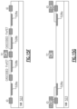
FIG. 15A is a plan view of a FinFET thyristor protection structure according to another embodiment.
FIG. 15B is a cross section of the FinFET thyristor protection structure of FIG. 15A taken along the lines 15B-15B.
FIG. 15C is a cross section of the FinFET thyristor protection structure of FIG. 15A taken along the lines 15C-15C.
FIG. 15D is a cross section of the FinFET thyristor protection structure of FIG. 15A taken along the lines 15D-15D.
FIG. 15E is a cross section of the FinFET thyristor protection structure of FIG. 15A taken along the lines 15E-15E.
FIG. 15F is a cross section of the FinFET thyristor protection structure of FIG. 15A taken along the lines 15F-15F.
FIG. 15G is a cross section of the FinFET thyristor protection structure of FIG. 15A taken along the lines 15G-15G.
FIG. 16 is a circuit diagram of a FinFET thyristor protection circuit according to another embodiment.
FIG. 17 is a plan view of a FinFET thyristor protection structure according to another embodiment.
FIG. 18A is a graph of one example of pre-sweep current versus voltage characteristics for one implementation of the FinFET thyristor protection structure of FIG. 4A.
FIG. 18B is a graph of one example of positive transmission line pulsing (TLP) measurements for one implementation of the FinFET thyristor protection structure of FIG. 4A.
FIG. 18C is a graph of another example of pre-sweep current versus voltage characteristics for one implementation of the FinFET thyristor protection structure of FIG. 4A.
FIG. 18D is a graph of one example of negative TLP measurements for one implementation of the FinFET thyristor protection structure of FIG. 4A.
FIG. 19A is a graph of one example of pre-sweep current versus voltage characteristics for one implementation of the FinFET thyristor protection structure of FIG. 9A.
FIG. 19B is a graph of one example of positive TLP measurements for one implementation of the FinFET thyristor protection structure of FIG. 9A.
FIG. 19C is a graph of another example of pre-sweep current versus voltage characteristics for one implementation of the FinFET thyristor protection structure of FIG. 9A.
FIG. 19D is a graph of one example of negative TLP measurements for one implementation of the FinFET thyristor protection structure of FIG. 11A.
FIG. 20A is a graph of one example of pre-sweep current versus voltage characteristics for one implementation of the FinFET thyristor protection structure of FIG. 11A.
FIG. 20B is a graph of one example of positive TLP measurements for one implementation of the FinFET thyristor protection structure of FIG. 11A.
FIG. 20C is a graph of one example of voltage versus time characteristics for one implementation of the FinFET thyristor protection structure of FIG. 11A.
FIG. 20D is a graph of another example of pre-sweep current versus voltage characteristics for one implementation of the FinFET thyristor protection structure of FIG. 11A.
FIG. 20E is a graph of one example of negative TLP measurements for one implementation of the FinFET thyristor protection structure of FIG. 11A.
FIG. 20F is a graph of another example of voltage versus time characteristics for one implementation of the FinFET thyristor protection structure of FIG. 11A.
FIG. 21A is a graph of one example of pre-sweep current versus voltage characteristics for one implementation of the FinFET thyristor protection structure of FIG. 15A.
FIG. 21B is a graph of one example of positive TLP measurements for one implementation of the FinFET thyristor protection structure of FIG. 15A.
FIG. 21C is a graph of one example of voltage versus time characteristics for one implementation of the FinFET thyristor protection structure of FIG. 15A.
FIG. 21D is a graph of another example of pre-sweep current versus voltage characteristics for one implementation of the FinFET thyristor protection structure of FIG. 15A.
FIG. 21E is a graph of one example of negative TLP measurements for one implementation of the FinFET thyristor protection structure of FIG. 15A.
FIG. 22 is a graph of one example of third-order intermodulation (IMD3) versus input power for a high-speed interface protected by various implementations of protection devices.
FIG. 23A is a graph of capacitance versus voltage for one implementation of a FinFET thyristor protection structure.
FIG. 23B is a graph of capacitance versus voltage for another implementation of a FinFET thyristor protection structure.
FIG. 23C is a graph of capacitance versus voltage for another implementation of a FinFET thyristor protection structure.
FIG. 24 is a circuit diagram of a FinFET thyristor protection circuit according to another embodiment.
FIG. 25 is a plan view of a FinFET thyristor protection structure according to another embodiment.
FIG. 26 is a circuit diagram of a FinFET thyristor protection circuit according to another embodiment.
FIG. 27 is a plan view of a FinFET thyristor protection structure according to another embodiment.
FIG. 28 is a circuit diagram of a FinFET thyristor protection circuit according to another embodiment.
FIG. 29 is a plan view of a FinFET thyristor protection structure according to another embodiment.
FIG. 30 is a circuit diagram of a FinFET thyristor protection circuit according to another embodiment.
FIG. 31 is a plan view of a FinFET thyristor protection structure according to another embodiment.
DETAILED DESCRIPTION
The following detailed description of embodiments presents various descriptions of specific embodiments of the invention. However, the invention can be embodied in a multitude of different ways in fin field-effect-transistor (FinFET) technology. In this description, reference is made to the drawings where like reference numerals may indicate identical or functionally similar elements. It will be understood that elements illustrated in the figures are not necessarily drawn to scale. Moreover, it will be understood that certain embodiments can include more elements than illustrated in a drawing and/or a subset of the elements illustrated in a drawing. Further, some embodiments can incorporate any suitable combination of features from two or more drawings.
Certain electronic systems include overstress protection circuits to protect circuits or components from electrical overstress events. To help guarantee that an electronic system is reliable, manufacturers can test the electronic system under defined stress conditions, which can be described by standards set by various organizations, such as the Joint Electronic Device Engineering Council (JEDEC), the International Electrotechnical Commission (IEC), and the Automotive Engineering Council (AEC). The standards can cover a wide multitude of electrical overstress events, including electrical overstress (EOS) and/or electrostatic discharge (ESD).
FIG. 1A is a schematic diagram of a high-speed receiver 20 with electrical overstress protection according to one embodiment. The receiver 20 includes a receiver front end 1, an in-phase (I) path transimpedance amplifier (TIA) 2 a, a quadrature-phase (Q) path TIA 2 b, an I path analog-to-digital converter (ADC) 3 a, a Q-path ADC 3 b, a digital baseband system 4, offset digital-to-analog converters (DACs) 5, and a TIA tuner 6.
As shown in FIG. 1A, the receiver front end 1 is coupled to a differential radio frequency input (RFIN) interface, and includes a first fin field-effect-transistor (FinFET) thyristor protection structure 11 a, a second FinFET thyristor protection structure 11 b, a receive attenuator 12, an I path mixer 13 a, a Q path mixer 13 b, and a tunable capacitor bank 14 including an I path tunable capacitor 15 a and a Q path tunable capacitor 15 b.
The high-speed receiver 20 illustrates one example application for the FinFET thyristor protection structures disclosed herein. For example, the first FinFET thyristor protection structure 11 a is connected between a non-inverted RF input of the RFIN interface and ground, while the second FinFET thyristor protection structure 11 b is connected between an inverted RF input of the RFIN interface and ground. The FinFET thyristor protection structures 11 a-11 b are turned off during normal operating conditions of the interface RFIN, but activate to provide overstress protection in response to an electrical overstress event.
As shown in FIG. 1A, the FinFET thyristor protection structures capacitively load the RFIN interface, even when turned off. By implementing the FinFET thyristor protection structures in accordance with the teachings herein, robust protection to the RFIN interface is provided while providing low parasitic capacitance to allow the interface to operate with high-speed and wide bandwidth.
Although FIG. 1A illustrates one example application for FinFET thyristor protection structures, the teachings herein are applicable to a wide variety of high-speed interfaces.
FIG. 1B is a schematic diagram of a high-speed transmitter 40 with electrical overstress protection according to one embodiment. The high-speed transmitter 40 includes a transmitter slice 21, an observation receiver slice 22, a first DC blocking capacitor 23 a, a second DC blocking capacitor 23 b, a first balun 24 a, and a second balun 24 b.
As shown in FIG. 1B, the transmitter slice 21 includes a DAC 25, a low pass filter 26, a mixer 27, and a first FinFET thyristor protection structure 28 a coupled between an output of the mixer 27 and ground. Additionally, the observation receiver 22 includes an ADC 29, a third DC blocking capacitor 23 c, a controllable attenuator 31 (for instance, a voltage variable attenuator or digital step attenuator), and a second FinFET thyristor protection structure 28 b connected between an input of the controllable attenuator 31 and ground.
The high-speed transmitter 40 illustrates another example application for the FinFET thyristor protection structures disclosed herein. Although FIG. 1B illustrates another example application for FinFET thyristor protection structures, the teachings herein are applicable to a wide variety of high-speed interfaces.
FIG. 1C is a schematic diagram of a fifth generation (5G) communication system 70 with electrical overstress protection according to one embodiment. The 5G communication system 70 illustrates another example application for FinFET thyristor protection structures. However, the teachings herein are applicable to other implementation of systems.
In the illustrated embodiment, the 5G communication system 70 includes a receiver 41, a transmitter 42 (with direct digital to RF (DRF) loopback, in this example), a DRF observation receiver 43, a baseband processor 44, an RF local oscillator (LO) phase-locked loop (PLL) 45, an LO generator 46, a serializer/deserializer (SERDES) PLL 47, serializers 48 (operating in compliance with JESD204B and/or JESD204C, in this example), a clock PLL 49, a first multiplexer 51 a (multiplexing between an external LO clock signal EXT_LO and a clock signal from the RF LO PLL 45, in this example), a second multiplexer 51 b, a third multiplexer 51 c, a fourth multiplexer 51 d (multiplexing between a clock PLL signal CLK PLL and a clock signal from the SERDES PLL 47, in this example), an RF receiver interface 52 a, an RF transmitter interface 52 b, an RF observation receiver interface 52 c, and a high-speed serializer interface 52 d.
As shown in FIG. 1C, the baseband processor 44 includes a receive data path 61 (for providing data recovered from the receiver 41 to SERDES), a loopback data path 62 (for processing data from DRF loopback of the transmitter 42), a transmit data path 63 (for processing data received from SERDES to generate data for the transmitter 42), an observation data path 64 (for calibrating the transmitter 42 based on observation data recovered from the observation receiver 43 and/or for providing the observation data to SERDES), and a JESD204B/JESD204C controller 65 (for controlling communications associated with the Joint Electron Devices Engineering Council (JESD) 204B and 204C standards).
In the illustrated embodiment, a wide variety of interfaces can be protected by the FinFET thyristor protection structures described herein. For example, the RF receiver interface 52 a, the RF transmitter interface 52 b, the RF observation receiver interface 52 c, and/or the high-speed serializer interface 52 d can be protected using the FinFET thyristor protection structures disclosed herein. However, the teachings herein are applicable to other implementations of high-speed interfaces.
In certain implementations, the 5G communication system 70 operates as part of a massive multi-input multiple-output (MIMO) system, which is a key communication infrastructure technology for delivering mobile 5G. For example, massive MIMO essentially groups together antennas at the transmitter and receiver to scale throughput and improve spectrum efficiency. Massive MIMO is used to multiply the capacity of wireless channels in a variety of communication standards, including not only 5G, but also 802.11n (Wi-Fi), 802.11ac (Wi-Fi), HSPA+, WiMAX, and LTE as well as other proprietary and non-proprietary communication standards.
There are significant design constraints to achieve robustness and performance trade-offs design targets in the main signal transmitter and receiver channels due to constraints in the operating voltage and capacitance linearity. To address limitations in existing art, a protection device that is high voltage tolerant, low capacitance, high linearity and robust to electrical overstress (including ESD) is critical in enabling reliable operation of these system. The protection device should provide little to no degradation to RF performance parameters such as second-order harmonic distortion (HD2), third-order harmonic distortion (HD3), third-order intermodulation distortion (IMD3), and/or third-order intercept point (IP3) at the required high power and/or small radio frequency (RF) signal. Furthermore, it is desirable for the protection device to behave linearly with respect to capacitance and current characteristics such that presence of the protection device does not interference with operation of the interface.
Conventional diode-based RF IO protection poses significant limitations in achieving RF performance for advancing 5G communication requirements while preserving interface robustness.
FIG. 2 is a perspective view of a fin field-effect transistor (FinFET) 80 according to one embodiment. The FinFET 80 is fabricated in a silicon (Si) substrate 71, and includes shallow trench isolation (STI) regions 72, source fins 73, drain fins 74, a gate fin 75, and a high-k metal gate (HKMG) region 76.
The FinFET 80 can provide a number of advantages relative to other transistor technologies. For example, the FinFET 80 facilitates higher level of integration and technology scaling, the FinFET 80 can provide higher electrical control over a channel, more effective leakage suppression, enhanced driving current, and/or higher intrinsic gain for superior analog performance.
Thus, the FinFET 80 provides a number of advantages suitable for deployment in ICs for high-speed data conversion, wide bandwidth wireless communications, and/or other high-performance applications. For example, a semiconductor chip implemented with FinFETs can be used to enable the high-speed applications discussed above with reference to FIGS. 1A-1C.
For example, to aid in meeting bandwidth constraints for 5G, it is desirable use FinFET technology to fabricate semiconductor dies (also referred to herein as integrated circuits or ICs) for high-performance transceivers and/or high-speed interfaces.
Although FinFET technology can provide a number of advantages, such FinFETs can operate with higher parasitic resistance, higher parasitic capacitance, and/or poorer thermal characteristics (for instance, higher thermal impedance and/or more self-heating) relative to transistors fabricated using a conventional complementary metal oxide semiconductor (CMOS) process. Such characteristics can render FinFETs susceptible to damage from electrical overstress. In addition, backend metallization interconnect introduces a relatively high parasitic capacitance the can account for over 40% of the total loading capacitance of the interface devices.
The teachings herein can be used to provide electrical overstress protection for ICs fabricated using FinFET technologies, thereby helping to meet tight design windows for robustness. For example, in certain embodiments herein, high voltage tolerant FinFET thyristors are provided for handling high stress current and high RF power handling capability, while providing low capacitance to allow wide bandwidth operation.
FIG. 3 is a circuit diagram of a FinFET thyristor protection circuit 120 according to one embodiment. The FinFET thyristor protection circuit 120 includes an NPN bipolar transistor 101, a PNP bipolar transistor 102, a FinFET gated NPN bipolar transistor 103, a FinFET gated PNP bipolar transistor 104, and a diode 105. One example connectivity of the FinFET thyristor protection circuit 120 to an input and/or output (TO) terminal, a substrate (SUB) terminal, and a ground (VSS) terminal is depicted.
In the illustrated embodiment, the FinFET thyristor protection circuit 120 provides electrical overstress protection between the IO terminal and the VSS terminal. In particular, the FinFET thyristor protection circuit 120 activates to provide overstress protection when a voltage difference between the VSS terminal and the IO terminal is greater than a trigger voltage. Although depicted as being connected between the IO terminal and the VSS terminal, the FinFET thyristor protection circuits herein can be connected in other ways.
The PNP bipolar transistor 102 and the NPN bipolar transistor 101 are cross-coupled to form a thyristor, which is also referred to herein as a silicon-controlled rectifier (SCR). In particular, a collector of the NPN bipolar transistor 101 is connected to a base of the PNP bipolar transistor 102, and a collector of the PNP bipolar transistor 102 is connected to a base of the NPN bipolar transistor 101. As shown in FIG. 3 , the thyristor includes an anode (corresponding to the emitter of the PNP bipolar transistor 102) connected to the VSS terminal and a cathode (corresponding to the emitter of the NPN bipolar transistor 101) connected to the IO terminal. Once the thyristor is activated, the cross-coupling provides regenerative feedback and low impedance between the VSS terminal and the IO terminal to provide overstress protection.
In addition to the thyristor associated with the PNP bipolar transistor 102 and the NPN bipolar transistor 101, the FinFET thyristor protection circuit 120 further includes FinFET triggering circuitry that provides a current path between the VSS terminal and the IO terminal. The FinFET triggering circuitry includes the FinFET gated NPN bipolar transistor 103 and the FinFET gated PNP bipolar transistor 104, in this embodiment. The current path provided by the FinFET triggering circuitry serves to provide overstress protection during a time period before the thyristor is activated, to enhance turn-on speed of the thyristor by providing current to the bases of the thyristor's bipolar transistors, and/or to reduce total on-state resistance of the FinFET thyristor protection circuit 120 after the thyristor has activated (by providing a first current path through the FinFET triggering circuitry and a second current path through the thyristor).
As shown in FIG. 3 , the FinFET gated NPN bipolar transistor 103 includes an emitter connected to the IO terminal, and a base and a collector connected to one another. Additionally, the FinFET gated PNP bipolar transistor 104 includes an emitter connected to the VSS terminal, and a base and a collector connected to one another and to the bases of the NPN bipolar transistor 101, the PNP bipolar transistor 102, and the FinFET gated NPN bipolar transistor 103. The FinFET gated PNP bipolar transistor 104 and the FinFET gated NPN bipolar transistor 103 each include a gate structure (at least one gate fin corresponding to those used to fabricate fins of FETs in a FinFET manufacturing process), which are electrically floating in this embodiment.
Thus, although the FinFET triggering circuitry of FIG. 3 includes gate fins, the FinFET triggering circuitry of FIG. 3 does not include any FETs. As will be discussed later, certain embodiments of FinFET triggering circuitry herein do include actual FETs.
Implementing the FinFET thyristor protection circuit of FIG. 3 with the FinFET triggering circuitry provides a current path between the VSS terminal and the IO terminal. For example, the base-emitter junction of the FinFET gated NPN bipolar transistor 103 is associated with a first FinFET gated diode 107 including an anode connected to the base of the NPN bipolar transistor 101 and a cathode connected to the IO terminal. Additionally, the base-emitter junction of the FinFET gated PNP bipolar transistor 104 is associated with a second FinFET gated diode 108 including an anode connected to the VSS terminal and a cathode connected to the base of the NPN bipolar transistor 101.
Thus, the first FinFET gated diode 107 and the second FinFET gated diode 108 are in series between the VSS terminal and the IO terminal. The first FinFET gated diode 107 and the second FinFET gated diode 108 provide a dual diode (DD) response, which is in addition to the thyristor response provided by the NPN bipolar transistor 101 and the PNP bipolar transistor 102. Thus, the FinFET thyristor protection circuit 120 is also referred to herein as a FinFET DD-thyristor.
Using a gated diode provides a number of advantages, such as reduced leakage current, lower parasitic capacitance, and/or higher holding voltage relative to a p-n junction diode with no gate structure over the p-n junction. Furthermore, a gated diode can have superior low capacitance characteristics in the presence of PVT variation. In certain implementations herein, the gate of a gated diode or gated bipolar transistor is electrically floating during operation.
In certain implementations, the bases and collectors of the FinFET gated PNP bipolar transistor 103 and the FinFET gated NPN bipolar transistor 104 are connected to one another in metallization using a conductor TC.
In certain implementations, the base of the PNP bipolar transistor 102 is associated with an n-type well (NW)/deep n-type well (DNW), while the base of the NPN bipolar transistor 101 is associated with a p-type well (PW) that is isolated from a p-type substrate (and the terminal SUB) by the DNW. In such implementations, the diode 105 is present between the p-type substrate and the NW/DNW.
The FinFET thyristor protection circuit 120 has been annotated to depict various resistors that can be present between various nodes of the FinFET thyristor protection circuit 120. The resistors can correspond to resistances of metallization, n-type semiconductor regions, and/or p-type semiconductor regions.
FIGS. 4A-4E illustrate one embodiment of a FinFET thyristor protection structure 150 that can be included in electrical overstress protection circuitry for a chip interface. FIG. 4A is a plan view of the FinFET thyristor protection structure 150. FIG. 4B is a cross section of the FinFET thyristor protection structure 150 of FIG. 4A taken along the lines 4B-4B. FIG. 4C is a cross section of the FinFET thyristor protection structure 150 of FIG. 4A taken along the lines 4C-4C. FIG. 4D is a cross section of the FinFET thyristor protection structure 150 of FIG. 4A taken along the lines 4D-4D. FIG. 4E is a cross section of the FinFET thyristor protection structure 150 of FIG. 4A taken along the lines 4E-4E.
The FinFET thyristor protection structure 150 illustrates one embodiment of a chip layout used to implement the FinFET thyristor protection circuit 120 of FIG. 3 . However, the FinFET thyristor protection circuit 120 of FIG. 3 can be implemented in other ways. One or more instantiations of the FinFET thyristor protection structure 150 can be included on a semiconductor die to protect circuitry of the die's interface from damage arising from electrical overstress events, such as ESD events.
The FinFET thyristor protection structures herein can include various wells (for instance, n-type well (NW) and/or p-type well (PW) regions), various active regions (for instance, n-type active (N+) and/or p-type active (P+) regions), gates, and/or other structures. As persons of ordinary skill in the art will appreciate, P+ regions have a higher doping concentration than the PWs. Additionally, N+ regions have a higher doping concentration than NWs. Persons having ordinary skill in the art will appreciate various concentrations of dopants in the regions.
It should be appreciated that because regions within a semiconductor device are defined by doping different parts of a semiconductor material with differing impurities or differing concentrations of impurities, discrete physical boundaries between different regions may not actually exist in the completed device but instead regions may transition from one to another. Some boundaries as shown in the figures of this type and are illustrated as abrupt structures merely for the assistance of the reader. As persons having ordinary skill in the art will appreciate, p-type regions can include a p-type semiconductor material, such as boron, as a dopant. Furthermore, n-type regions can include an n-type semiconductor material, such as phosphorous, as a dopant.
With reference to FIGS. 4A-4E, the FinFET thyristor protection structure 150 is fabricated in a p-type substrate (PSUB) 121. Additionally, a deep n-type well (DNW) 122 is formed in the PSUB 121, and an NW 123 and a PW 124 are formed adjacent to one another in the DNW 122. The DNW 122 and PSUB 121 are not depicted in the cross-sections.
A first group of P+ regions 125 a and a second group of P+ regions 125 b are formed in the NW 123. Additionally, a first group of N+ regions 126 a and a second group of N+ regions 126 b are formed in the PW 124. Furthermore, a third group of N+ regions 126 c is formed in the NW 123 between the first group of P+ regions 125 a and the second group of P+ regions 125 b. Additionally, a third group of P+ regions 125 c is formed in the PW 124 between the first group of N+ regions 126 a and the second group of N+ regions 126 b. Additionally, a first group of gate fin regions 128 a is formed over the NW 123 and a second group of gate fin regions 128 b is formed over the PW 124. Various metallization including metal zero routes (M0PO and M0OD), metal one routes (M1), and vias and contacts are depicted. Although various numbers of device fingers are shown, other numbers of device fingers are possible, such as a number of fingers selected to achieve desired current handling.
The cross sections are also annotated to show various devices formed from the layout. The devices correspond to those of the FinFET thyristor protection circuit 120 of FIG. 3 .
For example, the FinFET thyristor protection structure 150 includes an NPN bipolar transistor 101 having an emitter, a base, and a collector corresponding to the N+ regions 126 a-126 b, the PW 124, and the NW 123, respectively. Additionally, the FinFET thyristor protection structure 150 includes a PNP bipolar transistor 102 having an emitter, a base, and a collector corresponding to the P+ regions 125 a-125 b, the NW 123, and the PW 124, respectively.
With continuing reference to FIGS. 4A-4E, the FinFET thyristor protection structure 150 further includes a FinFET gated NPN bipolar transistor 103 having an emitter, a base, a collector, and a gate associated with N+ regions 126 a-126 b, PW 124, NW 123, and gate fin regions 128 b, respectively. The base-emitter junction of the FinFET gated NPN bipolar transistor 103 corresponds to a first FinFET gated diode 107 having an anode, a cathode, and a gate associated with PW 124, N+ regions 126 a-126 b, and gate fin regions 128 b, respectively. Additionally, the FinFET thyristor protection structure 150 further includes a FinFET gated PNP bipolar transistor 104 having an emitter, a base, a collector, and a gate associated with P+ regions 125 a-125 b, NW 123, PW 124, and gate fin regions 128 a, respectively. The base-emitter junction of the FinFET gated PNP bipolar transistor 104 corresponds to a second FinFET gated diode 108 having an anode, a cathode, and a gate associated with P+ regions 125 a-125 b, NW 123, and gate fin regions 128 a, respectively.
A conductor TC is used to connect the anode of first FinFET gated diode 107 to the cathode of the second FinFET gated diode 108, and thus the first FinFET gated diode 107 and the second FinFET gated diode 108 are connected in series between the IO terminal and the VSS terminal to provide the FinFET thyristor protection structure 150 with a dual diode response.
In the illustrated embodiment, conduction of the dual diode response is in a first direction, while conduction of the thyristor is in a second direction that is substantially perpendicular to the first direction. For example, with respect to the page orientation of FIG. 4A, conduction through the first FinFET gated diode 107 and the second FinFET gated diode 108 is lateral, while conduction through the thyristor is vertical. Implementing the FinFET thyristor protection structure 150 in this manner increases total current handling capability and mitigates issues arising from overheating.
FIG. 5 is a plan view of an array 160 of the FinFET thyristor protection structures of FIG. 4A. As shown in FIG. 5 , multiple PWs are formed in the NW and separated from one another. Additionally, a first FinFET thyristor protection structure 150 a, a second FinFET thyristor protection structure 150 b, a third FinFET thyristor protection structure 150 c, and a fourth FinFET thyristor protection structure 150 d are depicted.
Although four FinFET thyristor protection structures are depicted, more and fewer can be included as indicated by the ellipsis.
The array 160 includes multiple FinFET thyristor protection structures that have been replicated. Additionally, metallization can be used to connect the corresponding terminals of the FinFET thyristor protection structures to one another. By implementing the array 160 in this manner, a desired amount of current handling can be achieved using a layout that is compact for small area, low parasitic capacitance, and/or flexibility to control or configure current handling capability. Any of the FinFET thyristor protection structures herein can be arranged in an array.
FIG. 6 is a schematic diagram of a high-speed transceiver interface 200 protected using instantiations of the FinFET thyristor protection circuit 120 of FIG. 3 .
As shown in FIG. 6 , the interface 200 includes a transceiver 191 that is coupled to a high-speed input and/or output (HS IO) pin. To protect the interface from damage, a first FinFET thyristor protection circuit 120 a is connected between a power supply (VDD) pin and the HS IO pin, and a second FinFET thyristor protection circuit 120 b is connected between the HS IO pin and a ground (VSS) pin. A power supply clamp 192 is also included between the VDD pin and the VSS pin.
The first FinFET thyristor protection circuit 120 a and the second FinFET protection structure 120 b are each implemented using an instantiation of the FinFET thyristor protection circuit 120 of FIG. 3 .
For example, the first FinFET thyristor protection circuit 120 a includes an NPN bipolar transistor 101 a, a PNP bipolar transistor 102 a, a FinFET gated NPN bipolar transistor 103 a, a FinFET gated PNP bipolar transistor 104 a, and a diode 105 a. Additionally, the second FinFET thyristor protection circuit 120 b includes an NPN bipolar transistor 101 b, a PNP bipolar transistor 102 b, a FinFET gated NPN bipolar transistor 103 b, a FinFET gated PNP bipolar transistor 104 b, and a diode 105 b.
FIG. 7A is a schematic diagram of a bidirectional FinFET thyristor protection structure 210. The bidirectional FinFET thyristor protection structure 210 includes a forward thyristor protection structure 201 and a reverse thyristor protection structure 202 connected in parallel with one another between a first terminal and a second terminal. FIG. 7B is a graph of forward and reverse protection characteristics for the bidirectional FinFET thyristor protection structure 210 of FIG. 7A. The graph includes a voltage versus current plot depicting forward trigger voltage (Vtf), forward current (If), reverse trigger voltage Vtr, and reverse current (Jr).
With reference to FIGS. 7A and 7B, the forward protection characteristics of the bidirectional FinFET thyristor protection structure 210 are established by the forward thyristor protection structure 201, while the reverse protection characteristics of the bidirectional FinFET thyristor protection 210 are established by the reverse thyristor protection structure 202. Thus, the forward thyristor protection structure 201 provides little to no impact on reverse protection characteristics, while the reverse thyristor protection structure 202 provides little to no impact on forward protection characteristics.
Accordingly, the forward thyristor protection structure 201 can be designed/fine-tuned for high voltage tolerant operation to positive polarity overstress (increases the voltage of the first terminal relative to the second terminal) with very high blocking voltage for negative overstress. Additionally, the reverse thyristor protection structure 202 can be designed/fine-tuned for low trigger voltage operation to negative polarity overstress (decreases the voltage of the first terminal relative to the second terminal) with very high blocking voltage for positive polarity overstress. Thus, separate structures can be used to define forward and reverse protection characteristics.
Various FinFET thyristor protection structures herein can be used to define the forward or reverse characteristics of the bidirectional FinFET thyristor protection structure 210. Thus, the same or different types of FinFET thyristor protection structures can be used with connectivity made to proper terminals to achieve protection in a desired direction. In certain implementations herein, FinFET thyristor protection structures for reverse protection include DNW structures to aid in providing sufficient blocking voltage suitable for achieving a reverse protection characteristic.
FIG. 8 is a circuit diagram of a FinFET thyristor protection circuit 320 according to one embodiment. The FinFET thyristor protection circuit 320 includes an anode terminal, a cathode terminal, a first FinFET gated diode D1, a second FinFET gated diode D2, a third FinFET gated diode D3, a first bipolar transistor Q1 (p-type or PNP), a second bipolar transistor Q2 (n-type or NPN), a third bipolar transistor Q3 (PNP), a fourth bipolar transistor Q4 (NPN), a fifth bipolar transistor Q5 (PNP), and a sixth bipolar transistor Q6 (NPN). The revere thyristor protection circuit 320 illustrates one embodiment of a reverse protection circuit for establishing reverse protection characteristics of a bidirectional FinFET thyristor protection structure. However, other implementation of reverse protection structures are possible.
As shown in FIG. 8 , the first FinFET gated diode D1, the second FinFET gated diode D2, and the third FinFET gated diode D3 are connected in series, from anode to cathode, between the anode terminal and the cathode terminal. The first bipolar transistor Q1 and the second bipolar transistor Q2 operate as a first thyristor connected between the anode terminal and the anode of the third FinFET gated diode D3. Additionally, the third bipolar transistor Q3 and the fourth bipolar transistor Q4 operate as a second thyristor connected between the cathode of the first FinFET gated diode D1 and the cathode terminal. Furthermore, the fifth bipolar transistor Q5 and the sixth bipolar transistor Q6 operate as a third thyristor connected between the anode terminal and the cathode terminal.
The series combination of FinFET gated diodes in parallel with the third thyristor provides low trigger voltage operation to negative polarity overstress (decreases in the voltage of the cathode terminal relative to the anode terminal), with the series combination of FinFET gated diodes activating first. Additionally, the series combination of FinFET gated diodes provides with very high blocking voltage for positive polarity overstress (increases the voltage of the cathode terminal relative to the anode terminal).
FIG. 9A is a plan view of a FinFET thyristor protection structure 350 according to one embodiment. FIG. 9B is an annotated plan view of a portion 9B of the FinFET thyristor protection structure 350 of FIG. 9A. The FinFET thyristor protection structure 350 illustrates one embodiment of a chip layout used to implement the FinFET thyristor protection circuit 320 of FIG. 8 . However, the FinFET thyristor protection circuit 320 of FIG. 8 can be implemented in other ways. One or more instantiations of the FinFET thyristor protection structure 350 can be included on a semiconductor die for overstress protection.
With reference to FIGS. 9A-9B, the FinFET thyristor protection structure 350 is fabricated in a PSUB 321, and includes a DNW/NW 323 formed in the PSUB 321. The FinFET thyristor protection structure 350 further includes a first PW 324 a, a second PW 324 b, and a third PW 324 c each formed in the DNW/NW 323 and spaced apart from one another, with the second PW 324 b positioned between the first PW 324 a and the third PW 324 c. NW is not present where the first PW 324 a, the second PW 324 b, and the third PW 324 c are located, but DNW is present beneath the PWs.
With reference to the portion 9B shown in FIG. 9B, a first group of P+ regions 325 a and a first group of N+ regions 326 a are formed in the first PW 324 a. Additionally, a second group of P+ regions 325 b and a second group of N+ regions 326 b are formed in the second PW 324 b. Furthermore, a third group of P+ regions 325 c and a third group of N+ regions 326 c are formed in the third PW 324 c. Additionally, a first group of gate fin regions 328 a is formed over the first PW 324 a, a second group of gate fin regions 328 b is formed over the second PW 324 b, and a third group of gate fin regions 328 c is formed over the third PW 324 c. Various metallization is depicted.
The cross sections are also annotated to show various devices formed from the layout. The devices correspond to those of the FinFET thyristor protection circuit 320 of FIG. 8 .
For example, the FinFET thyristor protection structure 350 includes a first gated diode D1 having an anode, a cathode, and a gate associated with P+ regions 325 a, N+ regions 326 a, and gate fin regions 328 a, respectively. Additionally, the FinFET thyristor protection structure 350 includes a second gated diode D2 having an anode, a cathode, and a gate associated with P+ regions 325 b, N+ regions 326 b, and gate fin regions 328 b, respectively. Furthermore, the FinFET thyristor protection structure 350 includes a third gated diode D3 having an anode, a cathode, and a gate associated with P+ regions 325 c, N+ regions 326 c, and gate fin regions 328 c, respectively.
The FinFET thyristor protection structure 350 further includes a first bipolar transistor Q1 (PNP) having an emitter, a base, and a collector associated with PW 324 a, DNW/NW 323, and PW 324 b, respectively. Furthermore, the FinFET thyristor protection structure 350 further includes a second bipolar transistor Q2 (NPN) having an emitter, a base, and a collector associate with N+ regions 326 b, PW 324 b, and DNW/NW 323, respectively. Additionally, the FinFET thyristor protection structure 350 further includes a third bipolar transistor Q3 (PNP) having an emitter, a base, and a collector associated with the PW 324 b, the DNW/NW 323, and the PW 324 c, respectively. Furthermore, the FinFET thyristor protection structure 350 further includes a fourth bipolar transistor Q4 (NPN) having an emitter, a base, and a collector associated with the N+ regions 326 c, PW 324 c, and DNW/NW 323, respectively. Additionally, the FinFET thyristor protection structure 350 further includes a fifth bipolar transistor Q5 (PNP) having an emitter, a base, and a collector associated with the PW 324 a, the DNW/NW 323, and the PW 324 c, respectively. Furthermore, the FinFET thyristor protection structure 350 further includes a sixth bipolar transistor Q6 (NPN) having an emitter, a base, and a collector associated with the N+ regions 326 c, the PW 324 c and the DNW/NW 323, respectively.
FIG. 10 is a circuit diagram of a FinFET thyristor protection circuit 420 according to another embodiment. The FinFET thyristor protection circuit 420 includes an NPN bipolar transistor 401, a PNP bipolar transistor 402, a triggering PNP transistor 403, and a triggering p-type FinFET 405. One example connectivity of the FinFET thyristor protection circuit 420 to an IO terminal, a SUB terminal, and a VSS terminal is depicted. However, the FinFET thyristor protection circuit 420 can be connected between other terminals.
The PNP bipolar transistor 402 and the NPN bipolar transistor 401 are cross-coupled to form a thyristor. In addition to the thyristor, the FinFET thyristor protection circuit 420 further includes the triggering PNP bipolar transistor 403 and the triggering p-type FinFET 405, which aid in activating the thyristor, providing overstress protection during a time period before the thyristor is activated, and/or reducing total on-state resistance of the FinFET thyristor protection circuit 420 after the thyristor has activated.
As shown in FIG. 10 , the NPN bipolar transistor 401 includes an emitter connected to the VSS terminal, a base connected to a collector of the PNP bipolar transistor 402, and a collector connected to a base of the PNP bipolar transistor 402. The PNP bipolar transistor 402 further includes an emitter connected to the IO terminal. The triggering p-type FinFET 405 includes a body connected to a base of the PNP bipolar transistor 402, a drain connected to the base of the NPN bipolar transistor 401, and a source and a gate connected to the IO terminal. In certain implementations, the source to gate connection of the triggering p-type FinFET 405 is made in metallization. The triggering PNP bipolar transistor 403 includes an emitter connected to the IO terminal, a base connected to the body of the triggering p-type FinFET 405, and a collector connected to the drain of the triggering p-type FinFET 405.
Although illustrated for an implementation in which the FinFET 405 is p-type, the teachings herein are also applicable to implementations in which the FinFET is n-type. Likewise, although the triggering PNP bipolar transistor 403 is p-type, the teachings herein are also applicable to implementations using triggering NPN bipolar transistors.
In response to overstress, the triggering p-type FinFET 405 and/or the triggering PNP bipolar transistor 403 activate to provide a current path for overstress protection. The current path is from the IO terminal to the VSS terminal through the triggering p-type FinFET 405 and/or the triggering PNP bipolar transistor 403 and the base-to-emitter junction of the NPN bipolar transistor 401. The FinFET thyristor protection circuit 420 is also referred to herein as a FinFET PNP triggered (PNP-T) thyristor.
FIGS. 11A-11G illustrate another embodiment of a FinFET thyristor protection structure 450. FIG. 11A is a plan view of the FinFET thyristor protection structure 450. FIG. 11B is a cross section of the FinFET thyristor protection structure 450 of FIG. 11A taken along the lines 11B-11B. FIG. 11C is a cross section of the FinFET thyristor protection structure 450 of FIG. 11A taken along the lines 11C-11C. FIG. 11D is a cross section of the FinFET thyristor protection structure 450 of FIG. 11A taken along the lines 11D-11D. FIG. 11E is a cross section of the FinFET thyristor protection structure 450 of FIG. 11A taken along the lines 11E-11E. FIG. 11F is a cross section of the FinFET thyristor protection structure 450 of FIG. 11A taken along the lines 11F-11F. FIG. 11G is a cross section of the FinFET thyristor protection structure 450 of FIG. 11A taken along the lines 11G-11G.
The FinFET thyristor protection structure 450 of FIGS. 11A-11G illustrates one embodiment of a chip layout used to implement the FinFET thyristor protection circuit 420 of FIG. 10 . However, the FinFET thyristor protection circuit 420 of FIG. 10 can be implemented in other ways.
With reference to FIGS. 11A-11G, the FinFET thyristor protection structure 450 is fabricated in a PSUB 421, and includes an NW 423 and a PW 424 formed adjacent to one another in the PSUB 421.
A first group of P+ regions 425 a, a second group of P+ regions 425 b, and a third group of P+ regions 425 c are formed in the NW 423, with the second group of P+ regions 425 b positioned between the first group of P+ regions 425 a and the third group of P+ regions 425 c. Additionally, a first group of N+ regions 426 a, a fourth group of P+ regions 425 d, and a second group of N+ regions 426 b are formed in the PW 424, with the fourth group of P+ regions 425 d positioned between the first group of N+ regions 426 a and the second group of N+ regions 426 b. Additionally, a first group of gate fin regions 428 a is formed over the NW 423 and a second group of gate fin regions 428 b is formed over the PW 424. Various metallization including metal zero routes (M0PO and M0OD), metal one routes (M1), and vias and contacts are depicted.
The cross sections are also annotated to show various devices formed from the layout. The devices correspond to those of the FinFET thyristor protection circuit 420 of FIG. 10 .
For example, the FinFET thyristor protection structure 450 includes an NPN bipolar transistor 401 having an emitter, a base, and a collector corresponding to the N+ regions 426 a-426 b, the PW 424, and the NW 423, respectively. Additionally, the FinFET thyristor protection structure 450 includes a PNP bipolar transistor 402 having an emitter, a base, and a collector corresponding to the P+ regions 425 a/425 c, the NW 423, and the PW 424, respectively.
With continuing reference to FIGS. 11A-11G, the FinFET thyristor protection structure 450 further includes a triggering p-type FinFET 405 having a body, a source, a gate, and a drain associated with NW 423, P+ regions 425 a/425 c, gate fin regions 428 a, and P+ regions 425 b, respectively. Additionally, the FinFET thyristor protection structure 450 further includes a triggering PNP bipolar transistor 403 having an emitter, a base, and a collector associated with P+ regions 425 a-425 b, NW 423, and PW 424, respectively. A conductor TC is used to connect the PW 424 to the P+ regions 425 b, thereby connecting the collector of the triggering PNP bipolar transistor 403 to the drain of the triggering p-type FinFET 405 as well as to the base of the NPN bipolar transistor 401. FIG. 11G depicts the gate-to-source connection of the triggering p-type FinFET 405.
FIG. 12 is a circuit diagram of a FinFET thyristor protection circuit 460 according to another embodiment. The FinFET thyristor protection circuit 460 includes an NPN bipolar transistor 401, a PNP bipolar transistor 402, a triggering PNP transistor 403, a triggering p-type FinFET 405, a substrate PNP bipolar transistor 407, and a substrate diode 408. One example connectivity of the FinFET thyristor protection circuit 460 to an IO terminal, a SUB terminal, and a VSS terminal is depicted. However, the FinFET thyristor circuit 460 can be connected to other terminals.
The FinFET thyristor protection circuit 460 of FIG. 12 is similar to the FinFET thyristor protection circuit 420 of FIG. 10 , except that the FinFET thyristor protection circuit 460 further includes the substrate PNP bipolar transistor 407 and the substrate diode 408, which are associated with isolating the FinFET thyristor protection circuit 420 of FIG. 10 from a PSUB using a DNW isolation tub. Furthermore, in certain implementations, a PW guard ring is included around the DNW isolation tub to reduce carrier injection into the PSUB. The FinFET thyristor protection circuit 460 of FIG. 12 is also referred to herein as an ISO FinFET PNP-T thyristor.
FIG. 13 is a plan view of a FinFET thyristor protection structure 470 according to another embodiment. The FinFET thyristor protection structure 470 of FIG. 13 illustrates one embodiment of a chip layout used to implement the FinFET thyristor protection circuit 460 of FIG. 12 . However, the FinFET thyristor protection circuit 460 of FIG. 12 can be implemented in other ways.
The FinFET thyristor protection structure 470 of FIG. 13 is similar to the FinFET thyristor protection structure 450 of FIGS. 11A-11G, except that the FinFET thyristor protection structure 470 further includes a DNW 422.
FIG. 14 is a circuit diagram of a FinFET thyristor protection circuit 520 according to another embodiment. The FinFET thyristor protection circuit 520 includes an NPN bipolar transistor 501, a PNP bipolar transistor 502, a triggering PNP transistor 503, a first stacked PNP transistor 504 a, a second stacked PNP transistor 504 b, a first stacked p-type FinFET 505 a, and a second stacked p-type FinFET 505 b. The stacked FinFETs are also referred to herein as cascoded FinFETs. One example connectivity of the FinFET thyristor protection circuit 520 to an IO terminal, a SUB terminal, and a VSS terminal is depicted. However, the FinFET thyristor circuit 520 can be connected to other terminals.
The PNP bipolar transistor 502 and the NPN bipolar transistor 501 are cross-coupled to form a thyristor. In addition to the thyristor, the FinFET thyristor protection circuit 520 further includes FinFET triggering circuitry that aids in activating the thyristor, providing overstress protection during a time period before the thyristor is activated, and/or reducing total on-state resistance of the FinFET thyristor protection circuit 520 after the thyristor has activated. The FinFET triggering circuitry includes the triggering PNP bipolar transistor 503, the first stacked PNP transistor 504 a, the second stacked PNP transistor 504 b, the first stacked p-type FinFET 505 a, and the second stacked p-type FinFET 505 b.
As shown in FIG. 14 , the NPN bipolar transistor 501 includes an emitter connected to the VSS terminal, a base connected to a collector of the PNP bipolar transistor 502, and a collector connected to a base of the PNP bipolar transistor 502. The PNP bipolar transistor 502 further includes an emitter connected to the IO terminal. The first stacked p-type FinFET 505 a includes a body connected to a base of the first stacked PNP bipolar transistor 504 a, a drain connected to a collector of the first stacked PNP bipolar transistor 504 a, and a source and a gate connected to the IO terminal and to an emitter of the first stacked PNP bipolar transistor 504 a. In certain implementations, the source to gate connection of the first stacked p-type FinFET 505 a is made in metallization. The second stacked p-type FinFET 505 b includes a body connected to a base of the second stacked PNP bipolar transistor 504 b, a drain connected to a collector of the second stacked PNP bipolar transistor 504 b, and a source and a gate connected to an emitter of the second stacked PNP bipolar transistor 504 a and to the drain of the first stacked p-type FinFET 505 a. In certain implementations, the source to gate connection of the second stacked p-type FinFET 505 b is made in metallization.
As shown in FIG. 14 , the triggering PNP bipolar transistor 503 includes an emitter electrically connected to the IO terminal, a base connected to the bases of the stacked PNP bipolar transistors 504 a-504 b, and a collector connected to the base of the NPN bipolar transistor 501 and to the collector of the second stacked PNP bipolar transistor 504 b.
Although illustrated for an implementation in which the FinFET triggering circuitry is p-type, the teachings herein are also applicable to implementations using n-type devices or a combination of n-type and p-type devices.
In response to overstress, the FinFET triggering circuitry activates to provide a current path for overstress protection. The current path is from the IO terminal to the VSS terminal through the FinFET triggering circuitry and the base-to-emitter junction of the NPN bipolar transistor 501. The FinFET thyristor protection circuit 520 is also referred to herein as a stacked FinFET (ST-FinFET) PNP triggered (PNP-T) thyristor.
Inclusion of stacked FinFET devices aids in providing a mechanism for fine-tuning the protection characteristics and/or for providing greater robustness to high RF power.
FIGS. 15A-15G illustrate another embodiment of a FinFET thyristor protection structure 550. FIG. 15A is a plan view of the FinFET thyristor protection structure 550. FIG. 15B is a cross section of the FinFET thyristor protection structure 550 of FIG. 15A taken along the lines 15B-15B. FIG. 15C is a cross section of the FinFET thyristor protection structure 550 of FIG. 15A taken along the lines 15C-15C. FIG. 15D is a cross section of the FinFET thyristor protection structure 550 of FIG. 15A taken along the lines 15D-15D. FIG. 15E is a cross section of the FinFET thyristor protection structure 550 of FIG. 15A taken along the lines 15E-15E. FIG. 15F is a cross section of the FinFET thyristor protection structure 550 of FIG. 15A taken along the lines 15F-15F. FIG. 15G is a cross section of the FinFET thyristor protection structure 550 of FIG. 15A taken along the lines 15G-15G.
The FinFET thyristor protection structure 550 of FIGS. 15A-15G illustrates one embodiment of a chip layout used to implement the FinFET thyristor protection circuit 520 of FIG. 14 . However, the FinFET thyristor protection circuit 520 of FIG. 14 can be implemented in other ways.
With reference to FIGS. 15A-15G, the FinFET thyristor protection structure 550 is fabricated in a PSUB 521, and includes an NW 523 and a PW 524 formed adjacent to one another in the PSUB 521.
A first group of P+ regions 525 a, a second group of P+ regions 525 b, and a third group of P+ regions 525 c are formed in the NW 423, with the second group of P+ regions 525 b positioned between the first group of P+ regions 525 a and the third group of P+ regions 525 c (the P+ regions have horizontal mirror symmetry, in this embodiment). Additionally, a first group of N+ regions 526 a, a fourth group of P+ regions 525 d, and a second group of N+ regions 526 b are formed in the PW 524, with the fourth group of P+ regions 525 d positioned between the first group of N+ regions 526 a and the second group of N+ regions 526 b. Additionally, a first group of gate fin regions 528 a, a second group of gate fin regions 528 b, and a third group of gate fin regions 528 c are formed over the NW 523, while a fourth group of gate fin regions 528 d is formed over the PW 524. Various metallization including metal zero routes (M0PO and M0OD), metal one routes (M1), and vias and contacts are depicted.
The cross sections are also annotated to show various devices formed from the layout. The devices correspond to those of the FinFET thyristor protection circuit 520 of FIG. 14 .
For example, the FinFET thyristor protection structure 550 includes an NPN bipolar transistor 501 having an emitter, a base, and a collector corresponding to the N+ regions 526 a-526 b, the PW 524, and the NW 523, respectively. Additionally, the FinFET thyristor protection structure 550 includes a PNP bipolar transistor 502 having an emitter, a base, and a collector corresponding to the P+ regions 525 a, the NW 523, and the PW 524, respectively. Furthermore, the FinFET thyristor protection structure 550 further include a triggering PNP bipolar transistor 503 having an emitter, a base, and a collector associated with P+ regions 525 a, NW 523, and P+ regions 525 c.
With continuing reference to FIGS. 15A-15G, the FinFET thyristor protection structure 550 further includes a first stacked p-type FinFET 505 a having a body, a source, a gate, and a drain associated with NW 523, P+ regions 525 a, gate fin regions 528 a, and P+ regions 525 b, respectively. Additionally, the FinFET thyristor protection structure 550 further includes a first stacked PNP bipolar transistor 505 a having an emitter, a base, and a collector associated with P+ regions 525 a, NW 523, and P+ regions 525 b, respectively.
Furthermore the FinFET thyristor protection structure 550 further includes a second stacked p-type FinFET 505 b having a body, a source, a gate, and a drain associated with NW 523, P+ regions 525 b, gate fin regions 528 b, and P+ regions 525 c, respectively. Additionally, the FinFET thyristor protection structure 550 further includes a second stacked PNP bipolar transistor 505 b having an emitter, a base, and a collector associated with P+ regions 525 b, NW 523, and P+ regions 525 c, respectively. A conductor TC is used to connect the PW 524 to the P+ regions 525 b-525 c, thereby connecting the base of the NPN bipolar transistor 501 to the drain of the second stacked p-type FinFET 505 b, the collector of the second stacked PNP bipolar transistor 504 b, and to the collector of the PNP triggering bipolar transistor 503. FIGS. 15F and 15G depict the gate-to-source connections of the stacked p- type FinFETs 505 a and 505 b, respectively.
FIG. 16 is a circuit diagram of a FinFET thyristor protection circuit 560 according to another embodiment. The FinFET thyristor protection circuit 560 includes an NPN bipolar transistor 501, a PNP bipolar transistor 502, a triggering PNP transistor 503, a first stacked PNP bipolar transistor 504 a, a second stacked PNP bipolar transistor 504 b, a first stacked p-type FinFET 505 a, a second stacked p-type FinFET 505 b, a substrate PNP bipolar transistor 507, and a substrate diode 508. One example connectivity of the FinFET thyristor protection circuit 560 to an IO terminal, a SUB terminal, and a VSS terminal is depicted. However, the FinFET thyristor circuit 560 can be connected to other terminals.
The FinFET thyristor protection circuit 560 of FIG. 16 is similar to the FinFET thyristor protection circuit 520 of FIG. 14 , except that the FinFET thyristor protection circuit 560 further includes the substrate PNP bipolar transistor 507 and the substrate diode 508, which are associated with isolating the FinFET thyristor protection circuit 520 of FIG. 14 from a PSUB using a DNW isolation tub.
FIG. 17 is a plan view of a FinFET thyristor protection structure 570 according to another embodiment. The FinFET thyristor protection structure 570 of FIG. 17 illustrates one embodiment of a chip layout used to implement the FinFET thyristor protection circuit 560 of FIG. 16 . However, the FinFET thyristor protection circuit 560 of FIG. 16 can be implemented in other ways.
The FinFET thyristor protection structure 570 of FIG. 17 is similar to the FinFET thyristor protection structure 550 of FIGS. 15A-15G, except that the FinFET thyristor protection structure 570 further includes a DNW 522.
FIGS. 18A-18D are graphs of example measurement results for one implementation of the FinFET thyristor protection structure 150 of FIG. 4A. The graphs includes positive transmission line pulsing (TLP) measurements and negative TLP measurements for TLP testing with a 100 ns pulse width and a 600 ps rise time. Pre-sweep current versus voltage graphs are also included.
In the example shown in FIGS. 18A-18D, the FinFET thyristor protection structure 150 exhibits high reverse breakdown for IO to VSS conduction polarity as well as dual-diode thyristor activation at about 1.2 V for VSS to IO conduction polarity.
FIGS. 19A-19D are graphs of example measurement results for one implementation of the FinFET thyristor protection structure 350 of FIG. 9A. The graphs includes positive TLP measurements and negative TLP measurements for TLP testing with a 100 ns pulse width and a 600 ps rise time. Pre-sweep current versus voltage graphs are also included.
In the example shown in FIGS. 19A-19D, the FinFET thyristor protection structure 350 exhibits high blocking voltage for IO to VSS conduction polarity as well as high current conduction for VSS to IO conduction polarity.
FIGS. 20A-20F are graphs of example measurement results for one implementation of the FinFET thyristor protection structure 450 of FIG. 11A. The graphs includes positive TLP measurements and negative TLP measurements for TLP testing with a 100 ns pulse width and a 600 ps rise time. Pre-sweep current versus voltage graphs are also included. The graphs also include transient current versus voltage waveforms for both positive and negative overstress conditions.
FIGS. 21A-21E are graphs of example measurement results for one implementation of the FinFET thyristor protection structure 550 of FIG. 15A. The graphs includes positive TLP measurements and negative TLP measurements for TLP testing with a 100 ns pulse width and a 600 ps rise time. Pre-sweep current versus voltage graphs are also included. The graphs also include transient current versus voltage waveforms for a positive overstress condition.
FIG. 22 is a graph of one example of third-order intermodulation (IMD3) versus input power for a high-speed interface protected by various implementations of protection devices. The graph includes IMD3 performance for one implementation of the FinFET thyristor protection structure 150 of FIG. 4A versus two other designs. As shown in FIG. 22 , a maximum input power increase of over 10 dBm is achieved while still maintaining IMD3 specifications.
FIG. 23A is a graph of capacitance versus voltage for one implementation of a FinFET thyristor protection structure implemented to provide a current handling capability of greater than 600 mA TLP for greater than 2.5 A very fast TLP (VFTLP). As shown in FIG. 23A, less than 50 fF in capacitance is achieved for this current handling capability.
FIG. 23B is a graph of capacitance versus voltage for another implementation of a FinFET thyristor protection structure implemented to provide operation up to 2V and a current handling capability of greater than 2.5 A TLP for greater than 5.5 A TLP.
FIG. 23C is a graph of capacitance versus voltage for another implementation of a FinFET thyristor protection structure implemented to provide operation up to 2.5V and a current handling capability of greater than 2.5 A TLP for greater than 5.5 A TLP.
FIG. 24 is a circuit diagram of a FinFET thyristor protection circuit 620 according to another embodiment. The FinFET thyristor protection circuit 620 includes an NPN bipolar transistor 601, a PNP bipolar transistor 602, a triggering NPN transistor 603, and a triggering n-type FinFET 605. One example connectivity of the FinFET thyristor protection circuit 620 to an IO terminal, a SUB terminal, and a VSS terminal is depicted. However, the FinFET thyristor protection circuit 620 can be connected between other terminals.
The FinFET thyristor protection circuit 620 of FIG. 24 is similar the FinFET thyristor protection circuit 420 of FIG. 10 , except that the FinFET thyristor protection circuit 620 illustrates an n-type implementation of the FinFET triggering circuitry rather than a p-type implementation. In particular, the FinFET thyristor protection circuit 620 includes the triggering NPN transistor 603 and the triggering n-type FinFET 605 shown in FIG. 24 , rather than the triggering PNP transistor 403 and the triggering p-type FinFET 405 shown in FIG. 10 . The FinFET thyristor protection circuit 620 of FIG. 24 is also referred to herein as an FinFET NPN-T thyristor.
FIG. 25 is a plan view of a FinFET thyristor protection structure 650 according to another embodiment.
The FinFET thyristor protection structure 650 of FIG. 25 illustrates one embodiment of a chip layout used to implement the FinFET thyristor protection circuit 620 of FIG. 24 . However, the FinFET thyristor protection circuit 620 of FIG. 24 can be implemented in other ways.
With reference to FIG. 25 , the FinFET thyristor protection structure 650 is fabricated in a PSUB 621, and includes an NW 623 and a PW 624 formed adjacent to one another in the PSUB 621. Additionally, a first group of P+ regions 625 a, a second group of P+ regions 625 b, and a first group of N+ regions 626 a are formed in the NW 623, with the first group of N+ regions 626 a positioned between the first group of P+ regions 625 a and the second group of P+ regions 625 b. Additionally, a second group of N+ regions 626 b are formed in the PW 624. Additionally, a first group of gate fin regions 628 a is formed over the NW 623 and a second group of gate fin regions 628 b is formed over the PW 624. Various metallization including metal zero routes (M0PO and M0OD), metal one routes (M1), and vias and contacts are depicted.
FIG. 26 is a circuit diagram of a FinFET thyristor protection circuit 660 according to another embodiment. The FinFET thyristor protection circuit 660 includes an NPN bipolar transistor 601, a PNP bipolar transistor 602, a triggering NPN transistor 603, a triggering n-type FinFET 605, and a substrate diode 608. One example connectivity of the FinFET thyristor protection circuit 660 to an IO terminal, a SUB terminal, and a VSS terminal is depicted. However, the FinFET thyristor circuit 660 can be connected to other terminals.
The FinFET thyristor protection circuit 660 of FIG. 26 is similar to the FinFET thyristor protection circuit 620 of FIG. 24 , except that the FinFET thyristor protection circuit 660 further includes the substrate diode 608, which is associated with isolating the FinFET thyristor protection circuit 620 of FIG. 24 from a PSUB using a DNW isolation tub. The FinFET thyristor protection circuit 660 of FIG. 26 is also referred to herein as an ISO FinFET NPN-T thyristor.
FIG. 27 is a plan view of a FinFET thyristor protection structure 670 according to another embodiment. The FinFET thyristor protection structure 670 of FIG. 27 illustrates one embodiment of a chip layout used to implement the FinFET thyristor protection circuit 660 of FIG. 26 . However, the FinFET thyristor protection circuit 660 of FIG. 26 can be implemented in other ways.
The FinFET thyristor protection structure 670 of FIG. 27 is similar to the FinFET thyristor protection structure 650 of FIG. 25 , except that the FinFET thyristor protection structure 670 further includes a DNW 622.
FIG. 28 is a circuit diagram of a FinFET thyristor protection circuit 720 according to another embodiment. The FinFET thyristor protection circuit 720 includes an NPN bipolar transistor 701, a PNP bipolar transistor 702, a triggering NPN transistor 703, a first stacked NPN transistor 704 a, a second stacked NPN transistor 704 b, a first stacked n-type FinFET 705 a, and a second stacked n-type FinFET 705 b. One example connectivity of the FinFET thyristor protection circuit 720 to an IO terminal, a SUB terminal, and a VSS terminal is depicted. However, the FinFET thyristor circuit 720 can be connected to other terminals.
The FinFET thyristor protection circuit 720 of FIG. 28 is similar the FinFET thyristor protection circuit 520 of FIG. 14 , except that the FinFET thyristor protection circuit 720 illustrates an n-type implementation of the FinFET triggering circuitry rather than a p-type implementation. In particular, the FinFET thyristor protection circuit 720 includes the triggering NPN transistor 703, the first stacked NPN transistor 704 a, the second stacked NPN transistor 704 b, the first stacked n-type FinFET 705 a, and the second stacked n-type FinFET 705 b shown in FIG. 28 , rather than the triggering PNP transistor 503, the first stacked PNP transistor 504 a, the second stacked PNP transistor 504 b, the first stacked p-type FinFET 505 a, and the second stacked p-type FinFET 505 b shown in FIG. 14 . The FinFET thyristor protection circuit 720 of FIG. 28 is also referred to herein as an ST FinFET NPN-T thyristor.
FIG. 29 is a plan view of a FinFET thyristor protection structure 750 according to another embodiment. The FinFET thyristor protection structure 750 of FIG. 29 illustrates one embodiment of a chip layout used to implement the FinFET thyristor protection circuit 720 of FIG. 28 . However, the FinFET thyristor protection circuit 720 of FIG. 28 can be implemented in other ways.
With reference to FIG. 29 , the FinFET thyristor protection structure 750 is fabricated in a PSUB 721, and includes an NW 723 and a PW 724 formed adjacent to one another in the PSUB 721. Additionally, a first group of N+ regions 726 a, a second group of N+ regions 726 b, and a third group of N+ regions 726 c are formed in the PW 724, with the second group of N+ regions 726 b positioned between the first group of N+ regions 726 a and the third group of N+ regions 726 c. Additionally, a first group of P+ regions 725 a, a second group of P+ regions 725 b, and a fourth group of N+ regions 726 d are formed in the NW 723, with the fourth group of N+ regions 726 d positioned between the first group of P+ regions 725 a and the second group of P+ regions 725 b. Additionally, gate fin regions 728 a, gate fin regions 728 b, and gate fin regions 728 c are formed over the PW 724. Furthermore, gate fin regions 728 d are formed over NW 723. Various metallization including metal zero routes (M0PO and M0OD), metal one routes (M1), and vias and contacts are depicted.
FIG. 30 is a circuit diagram of a FinFET thyristor protection circuit 760 according to another embodiment. The FinFET thyristor protection circuit 760 includes an NPN bipolar transistor 701, a PNP bipolar transistor 702, a triggering NPN transistor 703, a first stacked NPN transistor 704 a, a second stacked NPN transistor 704 b, a first stacked n-type FinFET 705 a, a second stacked n-type FinFET 705 b, a substrate PNP bipolar transistor 707, and a substrate diode 708. One example connectivity of the FinFET thyristor protection circuit 760 to an IO terminal, a SUB terminal, and a VSS terminal is depicted. However, the FinFET thyristor circuit 760 can be connected to other terminals.
The FinFET thyristor protection circuit 760 of FIG. 30 is similar to the FinFET thyristor protection circuit 720 of FIG. 28 , except that the FinFET thyristor protection circuit 760 further includes the substrate PNP bipolar transistor 707 and the substrate diode 708, which are associated with isolating the FinFET thyristor protection circuit 720 of FIG. 28 from a PSUB using a DNW isolation tub. The FinFET thyristor protection circuit 760 of FIG. 30 is also referred to herein as an ISO-FinFET NPN-T thyristor.
FIG. 31 is a plan view of a FinFET thyristor protection structure 770 according to another embodiment. The FinFET thyristor protection structure 770 of FIG. 31 illustrates one embodiment of a chip layout used to implement the FinFET thyristor protection circuit 760 of FIG. 30 . However, the FinFET thyristor protection circuit 760 of FIG. 30 can be implemented in other ways.
The FinFET thyristor protection structure 770 of FIG. 31 is similar to the FinFET thyristor protection structure 750 of FIG. 29 , except that the FinFET thyristor protection structure 770 further includes a DNW 722.
Applications
Devices employing the above described schemes can be implemented into various electronic devices. Examples of the electronic devices can include, but are not limited to, consumer electronic products, parts of the consumer electronic products, electronic test equipment, communication infrastructure applications, etc. Further, the electronic device can include unfinished products, including those for communication, industrial, medical and automotive applications.
CONCLUSION
The foregoing description may refer to elements or features as being “connected” or “coupled” together. As used herein, unless expressly stated otherwise, “connected” means that one element/feature is directly or indirectly connected to another element/feature, and not necessarily mechanically. Likewise, unless expressly stated otherwise, “coupled” means that one element/feature is directly or indirectly coupled to another element/feature, and not necessarily mechanically. Thus, although the various schematics shown in the figures depict example arrangements of elements and components, additional intervening elements, devices, features, or components may be present in an actual embodiment (assuming that the functionality of the depicted circuits is not adversely affected).
While certain embodiments have been described, these embodiments have been presented by way of example only, and are not intended to limit the scope of the disclosure. Indeed, the novel apparatus, methods, and systems described herein may be embodied in a variety of other forms; furthermore, various omissions, substitutions and changes in the form of the methods and systems described herein may be made without departing from the spirit of the disclosure. For example, while the disclosed embodiments are presented in a given arrangement, alternative embodiments may perform similar functionalities with different components and/or circuit topologies, and some elements may be deleted, moved, added, subdivided, combined, and/or modified. Each of these elements may be implemented in a variety of different ways. Any suitable combination of the elements and acts of the various embodiments described above can be combined to provide further embodiments. Accordingly, the scope of the present invention is defined only by reference to the appended claims.
Although the claims presented here are in single dependency format for filing at the USPTO, it is to be understood that any claim may depend on any preceding claim of the same type except when that is clearly not technically feasible.

Claims (21)

What is claimed is:
1. A fin field-effect transistor (FinFET) thyristor protection structure for protecting a high-speed communication interface, the FinFET thyristor protection structure comprising:
a signal terminal and a ground terminal;
a thyristor comprising a PNP bipolar transistor and an NPN bipolar transistor that are cross-coupled, wherein the PNP bipolar transistor includes an emitter connected to the signal terminal and formed from a first plurality of p-type active (P+) regions in an n-type well (NW), a base formed from the NW, and a collector formed from a p-type well (PW), and wherein the NPN bipolar transistor includes an emitter connected to the ground terminal and formed from a first plurality of n-type active (N+) regions in the PW, a base formed from the PW, and a collector formed from the NW; and
FinFET triggering circuitry formed in the NW and the PW, wherein the FinFET triggering circuitry comprises a p-type FinFET having a source and a gate each connected to the signal terminal and a drain connected to the base of the NPN bipolar transistor, the p-type FinFET configured to activate to provide a current path from the signal terminal to the ground terminal in response to an electrical overstress event received between the signal terminal and the ground terminal, and to trigger activation of the thyristor in response to the electrical overstress event,
wherein the first plurality of P+ regions and the first plurality of N+ regions are each formed as fins extending in a first direction, and the gate of the p-type FinFET extends in a second direction substantially perpendicular to the first direction, the current path through the FinFET triggering circuitry in the first direction and a current path through the thyristor in the second direction,
wherein the drain of the p-type FinFET is formed in the NW and is connected to the base of the NPN bipolar transistor by a direct metal connection in the second direction.
2. The FinFET thyristor protection structure of claim 1, wherein the source of the p-type FinFET is formed from the first plurality of P+ regions in the NW, the drain of the p-type FinFET is formed from a second plurality of P+ regions, and the gate of the p-type FinFET is formed from a plurality of gate fins over the NW.
3. The FinFET thyristor protection structure of claim 2, wherein the gate and the source of the p-type FinFET are connected to one another in backend metallization.
4. A fin field-effect transistor (FinFET) thyristor protection circuit comprising:
a thyristor including an anode connected to a signal terminal and a cathode connected to a ground terminal, wherein the thyristor comprises a PNP bipolar transistor cross-coupled with an NPN bipolar transistor, wherein the PNP bipolar transistor includes an emitter connected to the signal terminal and the NPN bipolar transistor includes an emitter connected to the ground terminal, wherein the PNP bipolar transistor is formed from a first plurality of p-type active (P+) regions in an n-type well (NW) and the NPN bipolar transistor is formed from a first plurality of n-type active (N+) regions in the PW; and
FinFET triggering circuitry comprising a p-type FinFET having a source and a gate each connected to the signal terminal and a drain connected to a base of the NPN bipolar transistor, the p-type FinFET configured to activate to provide a current path from the signal terminal to the ground terminal in response to an electrical overstress event received between the signal terminal and the ground terminal,
wherein the FinFET triggering circuitry is further configured to trigger activation of the thyristor in response to the electrical overstress event,
wherein the first plurality of P+ regions and the first plurality of N+ regions are each formed as fins extending in a first direction, and the gate of the p-type FinFET extends in a second direction substantially perpendicular to the first direction, the current path through the FinFET triggering circuitry in the first direction and a current path through the thyristor in the second direction, and
wherein the drain of the p-type FinFET is formed in the NW and is connected to the base of the NPN bipolar transistor by a direct metal connection in the second direction.
5. The FinFET thyristor protection circuit of claim 4, wherein the FinFET triggering circuitry further comprises a triggering bipolar transistor having an emitter connected to the signal terminal, a base connected to a body of the p-type FinFET, and a collector connected to the base of the NPN bipolar transistor.
6. The FinFET thyristor protection circuit of claim 5, wherein a body of the p-type FinFET is connected to a base of the PNP bipolar transistor.
7. The FinFET thyristor protection circuit of claim 4, wherein the FinFET triggering circuitry further comprises a resistor connecting a substrate terminal to the drain of the p-type FinFET.
8. The FinFET thyristor protection circuit of claim 4, wherein a base-to-emitter junction of the PNP bipolar transistor is an open state.
9. The FinFET thyristor protection circuit of claim 4, wherein the current path through the p-type FinFET is substantially perpendicular to a current path through the thyristor.
10. The FinFET thyristor protection structure of claim 1, wherein the FinFET triggering circuitry further comprises a triggering bipolar transistor having an emitter connected to the signal terminal, a base connected to a body of the p-type FinFET, and a collector connected to the base of the NPN bipolar transistor.
11. The FinFET thyristor protection structure of claim 10, wherein the body of the p-type FinFET is connected to the base of the PNP bipolar transistor.
12. The FinFET thyristor protection structure of claim 1, further comprising a substrate terminal, wherein the FinFET triggering circuitry further comprises a resistor connecting the substrate terminal to the drain of the p-type FinFET, and the substrate terminal is decoupled from the ground terminal.
13. The FinFET thyristor protection structure of claim 1, wherein a base-to-emitter junction of the PNP bipolar transistor is an open state.
14. The FinFET thyristor protection structure of claim 1, wherein the first plurality of P+ regions in the NW are connected to a second plurality of P+ regions in the PW by a direct metal connection.
15. The FinFET thyristor protection structure of claim 14, wherein the source of the p-type FinFET is formed from the first plurality of P+ regions in the NW, and the drain of the p-type FinFET is formed from a third plurality of P+ regions in the NW.
16. The FinFET thyristor protection structure of claim 15, wherein the gate of the p-type FinFET is formed from a plurality of gate fins over the NW, the second plurality of P+ regions extend from the NW into the PW, the first plurality of N+ regions are positioned on a first side of the second plurality of P+ regions, and a third plurality of N+ regions are positioned on a second side of the second plurality of P+ regions opposite the first side.
17. The FinFET thyristor protection structure of claim 16, wherein each of the first plurality of P+ regions, the third plurality of P+ regions, the first plurality of N+ regions, and the third plurality of N+ regions extend a first distance in the first direction, wherein the second plurality of P+ regions extend a second distance in the first direction, wherein the first distance is greater than the second distance.
18. The FinFET thyristor protection structure of claim 17, wherein the second plurality of P+ regions extend in the second direction and are connected via a direct metal connection.
19. The FinFET thyristor protection structure of claim 1, wherein the source of the p-type FinFET is formed of a plurality of P+ regions, the drain of the p-type FinFET is formed of a plurality of P+ regions, the p-type FinFET has a second PNP bipolar transistor formed between the source and the drain of the p-type FinFET, the second PNP bipolar transistor configured to activate to provide the current path from the signal terminal to the ground terminal in response to an electrical overstress event received between the signal terminal and the ground terminal, and to trigger the activation of the thyristor through an independent current conduction path in response to the electrical overstress event.
20. The FinFET thyristor protection structure of claim 2, wherein the gate and the source of the p-type FinFET are connected to one another in backend metallization, and the first plurality of P+ regions forming the source of the of p-type FinFET is larger than the second plurality of p+ regions forming the drain of the p-type FinFET.
21. The FinFET thyristor protection structure of claim 1, wherein a body of the p-type FinFET is connected to the base of the PNP bipolar transistor and to the collector of the NPN bipolar transistor.
US16/863,830 2020-04-30 2020-04-30 FinFET thyristors for protecting high-speed communication interfaces Active US11595036B2 (en)

Priority Applications (5)

Application Number Priority Date Filing Date Title
US16/863,830 US11595036B2 (en) 2020-04-30 2020-04-30 FinFET thyristors for protecting high-speed communication interfaces
EP21797644.8A EP4143881A1 (en) 2020-04-30 2021-03-26 Finfet thyristors for protecting high-speed communication interfaces
KR1020227039604A KR20230004609A (en) 2020-04-30 2021-03-26 FINFET thyristors to protect high-speed communication interfaces
PCT/US2021/024363 WO2021221840A1 (en) 2020-04-30 2021-03-26 Finfet thyristors for protecting high-speed communication interfaces
US18/157,550 US20230163757A1 (en) 2020-04-30 2023-01-20 Finfet thyristors with embedded transistor control for protecting high-speed communication systems

Applications Claiming Priority (1)

Application Number Priority Date Filing Date Title
US16/863,830 US11595036B2 (en) 2020-04-30 2020-04-30 FinFET thyristors for protecting high-speed communication interfaces

Related Child Applications (1)

Application Number Title Priority Date Filing Date
US18/157,550 Division US20230163757A1 (en) 2020-04-30 2023-01-20 Finfet thyristors with embedded transistor control for protecting high-speed communication systems

Publications (2)

Publication Number Publication Date
US20210344336A1 US20210344336A1 (en) 2021-11-04
US11595036B2 true US11595036B2 (en) 2023-02-28

Family

ID=78293403

Family Applications (2)

Application Number Title Priority Date Filing Date
US16/863,830 Active US11595036B2 (en) 2020-04-30 2020-04-30 FinFET thyristors for protecting high-speed communication interfaces
US18/157,550 Pending US20230163757A1 (en) 2020-04-30 2023-01-20 Finfet thyristors with embedded transistor control for protecting high-speed communication systems

Family Applications After (1)

Application Number Title Priority Date Filing Date
US18/157,550 Pending US20230163757A1 (en) 2020-04-30 2023-01-20 Finfet thyristors with embedded transistor control for protecting high-speed communication systems

Country Status (4)

Country Link
US (2) US11595036B2 (en)
EP (1) EP4143881A1 (en)
KR (1) KR20230004609A (en)
WO (1) WO2021221840A1 (en)

Families Citing this family (1)

* Cited by examiner, † Cited by third party
Publication number Priority date Publication date Assignee Title
US11848321B2 (en) * 2021-04-23 2023-12-19 Taiwan Semiconductor Manufacturing Company Ltd. Semiconductor device for providing spike voltage protection and manufacturing method thereof

Citations (73)

* Cited by examiner, † Cited by third party
Publication number Priority date Publication date Assignee Title
US5610790A (en) 1995-01-20 1997-03-11 Xilinx, Inc. Method and structure for providing ESD protection for silicon on insulator integrated circuits
US20020089017A1 (en) 2001-01-05 2002-07-11 Lai Chun Hsiang Electostatic discharge protection circuit coupled on I/O pad
US6768616B2 (en) 2001-03-16 2004-07-27 Sarnoff Corporation Electrostatic discharge protection structures for high speed technologies with mixed and ultra-low voltage supplies
US7285828B2 (en) 2005-01-12 2007-10-23 Intersail Americas Inc. Electrostatic discharge protection device for digital circuits and for applications with input/output bipolar voltage much higher than the core circuit power supply
US7566914B2 (en) 2005-07-07 2009-07-28 Intersil Americas Inc. Devices with adjustable dual-polarity trigger- and holding-voltage/current for high level of electrostatic discharge protection in sub-micron mixed signal CMOS/BiCMOS integrated circuits
US7601991B2 (en) 2004-01-13 2009-10-13 Intersil Americas Inc. On-chip structure for electrostatic discharge (ESD) protection
US8044457B2 (en) 2009-06-29 2011-10-25 Analog Devices, Inc. Transient over-voltage clamp
US8222698B2 (en) 2009-06-29 2012-07-17 Analog Devices, Inc. Bond pad with integrated transient over-voltage protection
US8320091B2 (en) 2010-03-25 2012-11-27 Analog Devices, Inc. Apparatus and method for electronic circuit protection
US8368116B2 (en) 2010-06-09 2013-02-05 Analog Devices, Inc. Apparatus and method for protecting electronic circuits
US8416543B2 (en) 2010-07-08 2013-04-09 Analog Devices, Inc. Apparatus and method for electronic circuit protection
US8422187B2 (en) 2010-07-02 2013-04-16 Analog Devices, Inc. Apparatus and method for electronic circuit protection
US8432651B2 (en) 2010-06-09 2013-04-30 Analog Devices, Inc. Apparatus and method for electronic systems reliability
US8466489B2 (en) 2011-02-04 2013-06-18 Analog Devices, Inc. Apparatus and method for transient electrical overstress protection
US8553380B2 (en) 2010-07-08 2013-10-08 Analog Devices, Inc. Apparatus and method for electronic circuit protection
US8564065B2 (en) 2011-06-03 2013-10-22 Analog Devices, Inc. Circuit architecture for metal oxide semiconductor (MOS) output driver electrical overstress self-protection
US8570698B2 (en) 2009-02-19 2013-10-29 Taiwan Semiconductor Manufacturing Company, Ltd. ESD protection for FinFETs
US8592860B2 (en) 2011-02-11 2013-11-26 Analog Devices, Inc. Apparatus and method for protection of electronic circuits operating under high stress conditions
US8598641B2 (en) 2005-07-20 2013-12-03 International Business Machines Corporation Sea-of-fins structure on a semiconductor substrate and method of fabrication
US8610251B1 (en) 2012-06-01 2013-12-17 Analog Devices, Inc. Low voltage protection devices for precision transceivers and methods of forming the same
US8637899B2 (en) 2012-06-08 2014-01-28 Analog Devices, Inc. Method and apparatus for protection and high voltage isolation of low voltage communication interface terminals
US8665571B2 (en) 2011-05-18 2014-03-04 Analog Devices, Inc. Apparatus and method for integrated circuit protection
US8680620B2 (en) 2011-08-04 2014-03-25 Analog Devices, Inc. Bi-directional blocking voltage protection devices and methods of forming the same
US8779518B2 (en) 2012-12-04 2014-07-15 Taiwan Semiconductor Manufacturing Company, Ltd. Apparatus for ESD protection
US8796729B2 (en) 2012-11-20 2014-08-05 Analog Devices, Inc. Junction-isolated blocking voltage devices with integrated protection structures and methods of forming the same
US20140268438A1 (en) * 2013-03-12 2014-09-18 Micron Technology, Inc. Apparatuses and method for over-voltage event protection
US8860080B2 (en) 2012-12-19 2014-10-14 Analog Devices, Inc. Interface protection device with integrated supply clamp and method of forming the same
US20150008476A1 (en) * 2013-07-05 2015-01-08 Mayank Shrivastava Semiconductor devices and arrangements
US20150029622A1 (en) * 2013-07-26 2015-01-29 Taiwan Semiconductor Manufacturing Company, Ltd. Electrostatic discharge protection
US8946822B2 (en) 2012-03-19 2015-02-03 Analog Devices, Inc. Apparatus and method for protection of precision mixed-signal electronic circuits
US8947841B2 (en) 2012-02-13 2015-02-03 Analog Devices, Inc. Protection systems for integrated circuits and methods of forming the same
US8958187B2 (en) 2012-11-09 2015-02-17 Analog Devices, Inc. Active detection and protection of sensitive circuits against transient electrical stress events
US9006781B2 (en) 2012-12-19 2015-04-14 Analog Devices, Inc. Devices for monolithic data conversion interface protection and methods of forming the same
US9088256B2 (en) 2012-08-08 2015-07-21 Analog Devices, Inc. Apparatus and methods for amplifier fault protection
US9123540B2 (en) 2013-01-30 2015-09-01 Analog Devices, Inc. Apparatus for high speed signal processing interface
US9147677B2 (en) 2013-05-16 2015-09-29 Analog Devices Global Dual-tub junction-isolated voltage clamp devices for protecting low voltage circuitry connected between high voltage interface pins and methods of forming the same
US9171832B2 (en) 2013-05-24 2015-10-27 Analog Devices, Inc. Analog switch with high bipolar blocking voltage in low voltage CMOS process
US20160056146A1 (en) * 2014-08-21 2016-02-25 Apple Inc. Electrostatic Discharge (ESD) Silicon Controlled Rectifier (SCR) with Lateral Gated Section
US20160056147A1 (en) 2014-08-21 2016-02-25 Apple Inc. Single Junction Bi-Directional Electrostatic Discharge (ESD) Protection Circuit
US9275991B2 (en) 2013-02-13 2016-03-01 Analog Devices, Inc. Apparatus for transceiver signal isolation and voltage clamp
US9293912B2 (en) 2013-09-11 2016-03-22 Analog Devices, Inc. High voltage tolerant supply clamp
US20160141358A1 (en) * 2014-11-18 2016-05-19 Analog Devices, Inc. Apparatus and methods for transceiver interface overvoltage clamping
US20160204096A1 (en) 2015-01-12 2016-07-14 Analog Devices, Inc. Low leakage bidirectional clamps and methods of forming the same
US20160261110A1 (en) 2015-03-04 2016-09-08 Analog Devices, Inc. Apparatus and methods for overvoltage switches with active leakage current compensation
US20160285255A1 (en) 2015-03-27 2016-09-29 Analog Devices Global Electrical overstress recording and/or harvesting
US20160300830A1 (en) 2015-04-07 2016-10-13 Analog Devices, Inc. High speed interface protection apparatus
US20160336744A1 (en) 2015-05-15 2016-11-17 Analog Devices, Inc. Electrostatic discharge protection circuits for radio frequency communication systems
US20170069616A1 (en) 2015-09-08 2017-03-09 Hong Kong Applied Science & Technology Research Institute Company Limited Lateral-Diode, Vertical-SCR Hybrid Structure for High-Level ESD Protection
US9634482B2 (en) 2014-07-18 2017-04-25 Analog Devices, Inc. Apparatus and methods for transient overstress protection with active feedback
WO2017078676A1 (en) 2015-11-02 2017-05-11 Intel IP Corporation Transient triggered finfet silicon controlled rectifier for electrostatic discharge protection
US9653448B2 (en) 2014-07-17 2017-05-16 Apple Inc. Electrostatic discharge (ESD) diode in FinFET technology
US20170256534A1 (en) 2016-03-04 2017-09-07 Analog Devices, Inc. Apparatus and methods for actively-controlled transient overstress protection with false condition shutdown
US20170317070A1 (en) 2016-04-29 2017-11-02 Analog Devices Global Apparatuses for communication systems transceiver interfaces
US9876005B2 (en) 2015-10-01 2018-01-23 Taiwan Semiconductor Manufacturing Company, Ltd. SCRS with checker board layouts
US20180026440A1 (en) 2016-07-21 2018-01-25 Analog Devices, Inc. High voltage clamps with transient activation and activation release control
US20180068996A1 (en) 2015-12-21 2018-03-08 SK Hynix Inc. Electro-static discharge protection devices having a low trigger voltage
US20180158814A1 (en) 2016-12-06 2018-06-07 Analog Devices, Inc. Active interface resistance modulation switch
US20180158935A1 (en) 2016-12-07 2018-06-07 Qualcomm Incorporated Asymmetric gated fin field effect transistor (fet) (finfet) diodes
US20180211951A1 (en) 2017-01-24 2018-07-26 Analog Devices, Inc. Drain-extended metal-oxide-semiconductor bipolar switch for electrical overstress protection
US20180226788A1 (en) 2017-02-09 2018-08-09 Analog Devices, Inc. Distributed switches to suppress transient electrical overstress-induced latch-up
US10083952B2 (en) 2017-02-02 2018-09-25 Globalfoundries Inc. Diode-triggered schottky silicon-controlled rectifier for Fin-FET electrostatic discharge control
US20180308846A1 (en) * 2017-04-24 2018-10-25 Taiwan Semiconductor Manufacturing Co., Ltd. Capacitor cell and structure thereof
US10158029B2 (en) 2016-02-23 2018-12-18 Analog Devices, Inc. Apparatus and methods for robust overstress protection in compound semiconductor circuit applications
CN109166850A (en) 2018-10-09 2019-01-08 浙江大学昆山创新中心 The diode triggered of Integrated circuit electrostatic protection is silicon-controlled
US10177566B2 (en) 2016-06-21 2019-01-08 Analog Devices, Inc. Apparatus and methods for actively-controlled trigger and latch release thyristor
US20190013310A1 (en) 2017-02-01 2019-01-10 Indian Institute Of Science Dual fin silicon controlled rectifier (scr) electrostatic discharge (esd) protection device
US20190027470A1 (en) 2017-07-18 2019-01-24 Hong Kong Applied Science and Technology Research Institute Company, Limited Step Fin Field-Effect-Transistor (FinFET) with Slim Top of Fin and Thick Bottom of Fin for Electro-Static-Discharge (ESD) or Electrical Over-Stress (EOS) Protection
US10249609B2 (en) 2017-08-10 2019-04-02 Analog Devices, Inc. Apparatuses for communication systems transceiver interfaces
US20190131787A1 (en) 2017-10-26 2019-05-02 Analog Devices, Inc. Silicon controlled rectifier dynamic triggering and shutdown via control signal amplification
US10504886B1 (en) 2018-09-05 2019-12-10 Hong Kong Applied Science and Technology Research Institute Company, Limited Low-capacitance electro-static-discharge (ESD) protection structure with two floating wells
US20200111778A1 (en) 2018-10-04 2020-04-09 Nxp B.V. Gate-lifted nmos esd protection device
US20200286889A1 (en) 2019-03-06 2020-09-10 Analog Devices, Inc. Distributed electrical overstress protection for large density and high data rate communication applications
US20200403007A1 (en) * 2019-06-20 2020-12-24 Intel Corporation Substrate-less finfet diode architectures with backside metal contact and subfin regions

Patent Citations (80)

* Cited by examiner, † Cited by third party
Publication number Priority date Publication date Assignee Title
US5610790A (en) 1995-01-20 1997-03-11 Xilinx, Inc. Method and structure for providing ESD protection for silicon on insulator integrated circuits
US20020089017A1 (en) 2001-01-05 2002-07-11 Lai Chun Hsiang Electostatic discharge protection circuit coupled on I/O pad
US6768616B2 (en) 2001-03-16 2004-07-27 Sarnoff Corporation Electrostatic discharge protection structures for high speed technologies with mixed and ultra-low voltage supplies
US7601991B2 (en) 2004-01-13 2009-10-13 Intersil Americas Inc. On-chip structure for electrostatic discharge (ESD) protection
US7285828B2 (en) 2005-01-12 2007-10-23 Intersail Americas Inc. Electrostatic discharge protection device for digital circuits and for applications with input/output bipolar voltage much higher than the core circuit power supply
US7566914B2 (en) 2005-07-07 2009-07-28 Intersil Americas Inc. Devices with adjustable dual-polarity trigger- and holding-voltage/current for high level of electrostatic discharge protection in sub-micron mixed signal CMOS/BiCMOS integrated circuits
US8598641B2 (en) 2005-07-20 2013-12-03 International Business Machines Corporation Sea-of-fins structure on a semiconductor substrate and method of fabrication
US8570698B2 (en) 2009-02-19 2013-10-29 Taiwan Semiconductor Manufacturing Company, Ltd. ESD protection for FinFETs
US8044457B2 (en) 2009-06-29 2011-10-25 Analog Devices, Inc. Transient over-voltage clamp
US8222698B2 (en) 2009-06-29 2012-07-17 Analog Devices, Inc. Bond pad with integrated transient over-voltage protection
US8320091B2 (en) 2010-03-25 2012-11-27 Analog Devices, Inc. Apparatus and method for electronic circuit protection
US8368116B2 (en) 2010-06-09 2013-02-05 Analog Devices, Inc. Apparatus and method for protecting electronic circuits
US8432651B2 (en) 2010-06-09 2013-04-30 Analog Devices, Inc. Apparatus and method for electronic systems reliability
US8422187B2 (en) 2010-07-02 2013-04-16 Analog Devices, Inc. Apparatus and method for electronic circuit protection
US8553380B2 (en) 2010-07-08 2013-10-08 Analog Devices, Inc. Apparatus and method for electronic circuit protection
US8416543B2 (en) 2010-07-08 2013-04-09 Analog Devices, Inc. Apparatus and method for electronic circuit protection
US8466489B2 (en) 2011-02-04 2013-06-18 Analog Devices, Inc. Apparatus and method for transient electrical overstress protection
US8592860B2 (en) 2011-02-11 2013-11-26 Analog Devices, Inc. Apparatus and method for protection of electronic circuits operating under high stress conditions
US8665571B2 (en) 2011-05-18 2014-03-04 Analog Devices, Inc. Apparatus and method for integrated circuit protection
US8564065B2 (en) 2011-06-03 2013-10-22 Analog Devices, Inc. Circuit architecture for metal oxide semiconductor (MOS) output driver electrical overstress self-protection
US8680620B2 (en) 2011-08-04 2014-03-25 Analog Devices, Inc. Bi-directional blocking voltage protection devices and methods of forming the same
US8947841B2 (en) 2012-02-13 2015-02-03 Analog Devices, Inc. Protection systems for integrated circuits and methods of forming the same
US8946822B2 (en) 2012-03-19 2015-02-03 Analog Devices, Inc. Apparatus and method for protection of precision mixed-signal electronic circuits
US8610251B1 (en) 2012-06-01 2013-12-17 Analog Devices, Inc. Low voltage protection devices for precision transceivers and methods of forming the same
US8637899B2 (en) 2012-06-08 2014-01-28 Analog Devices, Inc. Method and apparatus for protection and high voltage isolation of low voltage communication interface terminals
US9088256B2 (en) 2012-08-08 2015-07-21 Analog Devices, Inc. Apparatus and methods for amplifier fault protection
US8958187B2 (en) 2012-11-09 2015-02-17 Analog Devices, Inc. Active detection and protection of sensitive circuits against transient electrical stress events
US8796729B2 (en) 2012-11-20 2014-08-05 Analog Devices, Inc. Junction-isolated blocking voltage devices with integrated protection structures and methods of forming the same
US8779518B2 (en) 2012-12-04 2014-07-15 Taiwan Semiconductor Manufacturing Company, Ltd. Apparatus for ESD protection
US8860080B2 (en) 2012-12-19 2014-10-14 Analog Devices, Inc. Interface protection device with integrated supply clamp and method of forming the same
US9006781B2 (en) 2012-12-19 2015-04-14 Analog Devices, Inc. Devices for monolithic data conversion interface protection and methods of forming the same
US9123540B2 (en) 2013-01-30 2015-09-01 Analog Devices, Inc. Apparatus for high speed signal processing interface
US9275991B2 (en) 2013-02-13 2016-03-01 Analog Devices, Inc. Apparatus for transceiver signal isolation and voltage clamp
US20140268438A1 (en) * 2013-03-12 2014-09-18 Micron Technology, Inc. Apparatuses and method for over-voltage event protection
US9147677B2 (en) 2013-05-16 2015-09-29 Analog Devices Global Dual-tub junction-isolated voltage clamp devices for protecting low voltage circuitry connected between high voltage interface pins and methods of forming the same
US9171832B2 (en) 2013-05-24 2015-10-27 Analog Devices, Inc. Analog switch with high bipolar blocking voltage in low voltage CMOS process
US20150008476A1 (en) * 2013-07-05 2015-01-08 Mayank Shrivastava Semiconductor devices and arrangements
US20150029622A1 (en) * 2013-07-26 2015-01-29 Taiwan Semiconductor Manufacturing Company, Ltd. Electrostatic discharge protection
US9293912B2 (en) 2013-09-11 2016-03-22 Analog Devices, Inc. High voltage tolerant supply clamp
US9653448B2 (en) 2014-07-17 2017-05-16 Apple Inc. Electrostatic discharge (ESD) diode in FinFET technology
US9634482B2 (en) 2014-07-18 2017-04-25 Analog Devices, Inc. Apparatus and methods for transient overstress protection with active feedback
US20160056146A1 (en) * 2014-08-21 2016-02-25 Apple Inc. Electrostatic Discharge (ESD) Silicon Controlled Rectifier (SCR) with Lateral Gated Section
US9318479B2 (en) 2014-08-21 2016-04-19 Apple Inc. Electrostatic discharge (ESD) silicon controlled rectifier (SCR) with lateral gated section
US20160056147A1 (en) 2014-08-21 2016-02-25 Apple Inc. Single Junction Bi-Directional Electrostatic Discharge (ESD) Protection Circuit
US9478608B2 (en) 2014-11-18 2016-10-25 Analog Devices, Inc. Apparatus and methods for transceiver interface overvoltage clamping
US20160141358A1 (en) * 2014-11-18 2016-05-19 Analog Devices, Inc. Apparatus and methods for transceiver interface overvoltage clamping
US20160204096A1 (en) 2015-01-12 2016-07-14 Analog Devices, Inc. Low leakage bidirectional clamps and methods of forming the same
US20160261110A1 (en) 2015-03-04 2016-09-08 Analog Devices, Inc. Apparatus and methods for overvoltage switches with active leakage current compensation
US20160285255A1 (en) 2015-03-27 2016-09-29 Analog Devices Global Electrical overstress recording and/or harvesting
US20160300830A1 (en) 2015-04-07 2016-10-13 Analog Devices, Inc. High speed interface protection apparatus
US20160336744A1 (en) 2015-05-15 2016-11-17 Analog Devices, Inc. Electrostatic discharge protection circuits for radio frequency communication systems
US20160336740A1 (en) 2015-05-15 2016-11-17 Analog Devices, Inc. Apparatus and methods for electrostatic discharge protection of radio frequency interfaces
US20170069616A1 (en) 2015-09-08 2017-03-09 Hong Kong Applied Science & Technology Research Institute Company Limited Lateral-Diode, Vertical-SCR Hybrid Structure for High-Level ESD Protection
US9876005B2 (en) 2015-10-01 2018-01-23 Taiwan Semiconductor Manufacturing Company, Ltd. SCRS with checker board layouts
WO2017078676A1 (en) 2015-11-02 2017-05-11 Intel IP Corporation Transient triggered finfet silicon controlled rectifier for electrostatic discharge protection
US20180068996A1 (en) 2015-12-21 2018-03-08 SK Hynix Inc. Electro-static discharge protection devices having a low trigger voltage
US10158029B2 (en) 2016-02-23 2018-12-18 Analog Devices, Inc. Apparatus and methods for robust overstress protection in compound semiconductor circuit applications
US20170256534A1 (en) 2016-03-04 2017-09-07 Analog Devices, Inc. Apparatus and methods for actively-controlled transient overstress protection with false condition shutdown
US10199369B2 (en) 2016-03-04 2019-02-05 Analog Devices, Inc. Apparatus and methods for actively-controlled transient overstress protection with false condition shutdown
US20170317070A1 (en) 2016-04-29 2017-11-02 Analog Devices Global Apparatuses for communication systems transceiver interfaces
US9831233B2 (en) 2016-04-29 2017-11-28 Analog Devices Global Apparatuses for communication systems transceiver interfaces
US10177566B2 (en) 2016-06-21 2019-01-08 Analog Devices, Inc. Apparatus and methods for actively-controlled trigger and latch release thyristor
US20180026440A1 (en) 2016-07-21 2018-01-25 Analog Devices, Inc. High voltage clamps with transient activation and activation release control
US20180158814A1 (en) 2016-12-06 2018-06-07 Analog Devices, Inc. Active interface resistance modulation switch
US10340370B2 (en) 2016-12-07 2019-07-02 Qualcomm Incorporated Asymmetric gated fin field effect transistor (FET) (finFET) diodes
US20180158935A1 (en) 2016-12-07 2018-06-07 Qualcomm Incorporated Asymmetric gated fin field effect transistor (fet) (finfet) diodes
US20180211951A1 (en) 2017-01-24 2018-07-26 Analog Devices, Inc. Drain-extended metal-oxide-semiconductor bipolar switch for electrical overstress protection
US20190013310A1 (en) 2017-02-01 2019-01-10 Indian Institute Of Science Dual fin silicon controlled rectifier (scr) electrostatic discharge (esd) protection device
US10083952B2 (en) 2017-02-02 2018-09-25 Globalfoundries Inc. Diode-triggered schottky silicon-controlled rectifier for Fin-FET electrostatic discharge control
US20180226788A1 (en) 2017-02-09 2018-08-09 Analog Devices, Inc. Distributed switches to suppress transient electrical overstress-induced latch-up
US20180308846A1 (en) * 2017-04-24 2018-10-25 Taiwan Semiconductor Manufacturing Co., Ltd. Capacitor cell and structure thereof
US20190027470A1 (en) 2017-07-18 2019-01-24 Hong Kong Applied Science and Technology Research Institute Company, Limited Step Fin Field-Effect-Transistor (FinFET) with Slim Top of Fin and Thick Bottom of Fin for Electro-Static-Discharge (ESD) or Electrical Over-Stress (EOS) Protection
US10249609B2 (en) 2017-08-10 2019-04-02 Analog Devices, Inc. Apparatuses for communication systems transceiver interfaces
US20190131787A1 (en) 2017-10-26 2019-05-02 Analog Devices, Inc. Silicon controlled rectifier dynamic triggering and shutdown via control signal amplification
US10504886B1 (en) 2018-09-05 2019-12-10 Hong Kong Applied Science and Technology Research Institute Company, Limited Low-capacitance electro-static-discharge (ESD) protection structure with two floating wells
US20200111778A1 (en) 2018-10-04 2020-04-09 Nxp B.V. Gate-lifted nmos esd protection device
CN109166850A (en) 2018-10-09 2019-01-08 浙江大学昆山创新中心 The diode triggered of Integrated circuit electrostatic protection is silicon-controlled
US20200286889A1 (en) 2019-03-06 2020-09-10 Analog Devices, Inc. Distributed electrical overstress protection for large density and high data rate communication applications
US11004849B2 (en) 2019-03-06 2021-05-11 Analog Devices, Inc. Distributed electrical overstress protection for large density and high data rate communication applications
US20200403007A1 (en) * 2019-06-20 2020-12-24 Intel Corporation Substrate-less finfet diode architectures with backside metal contact and subfin regions

Non-Patent Citations (2)

* Cited by examiner, † Cited by third party
Title
International Search Report and Written Opinion for International Application No. PCT/US2021/024363 dated Jul. 15, 2021, in 12 pages.
Karp et al., "FinFET MPSoC 32 GB/s transceivers: Custom ESD protection and verification." 2016 IEEE 59th International Midwest Symposium on Circuits and Systems (MWSCAS). IEEE, 2016, in 4 pages.

Also Published As

Publication number Publication date
WO2021221840A1 (en) 2021-11-04
EP4143881A1 (en) 2023-03-08
US20210344336A1 (en) 2021-11-04
KR20230004609A (en) 2023-01-06
US20230163757A1 (en) 2023-05-25

Similar Documents

Publication Publication Date Title
US9123540B2 (en) Apparatus for high speed signal processing interface
US9831666B2 (en) Apparatus and methods for electrostatic discharge protection of radio frequency interfaces
US10249609B2 (en) Apparatuses for communication systems transceiver interfaces
US8039899B2 (en) Electrostatic discharge protection device
US9006781B2 (en) Devices for monolithic data conversion interface protection and methods of forming the same
TWI405323B (en) Latch-up free vertical tvs diode array structure using trench isolation
US20160141358A1 (en) Apparatus and methods for transceiver interface overvoltage clamping
US8665570B2 (en) Diode having a pocket implant blocked and circuits and methods employing same
US8854778B2 (en) ESD protection circuit
US10211197B2 (en) Fabrication of radio-frequency devices with amplifier voltage limiting features
US9997511B2 (en) ESD protection circuit with plural avalanche diodes
US8531805B2 (en) Gated diode having at least one lightly-doped drain (LDD) implant blocked and circuits and methods employing same
US11342323B2 (en) High voltage tolerant circuit architecture for applications subject to electrical overstress fault conditions
US8981426B2 (en) Electrostatic discharge protection device
US11462535B2 (en) Distributed electrical overstress protection for large density and high data rate communication applications
US10930641B2 (en) Series connected ESD protection circuit
US20090072315A1 (en) Semiconductor Manufacturing Process Charge Protection Circuits
US20230163757A1 (en) Finfet thyristors with embedded transistor control for protecting high-speed communication systems
EP1423898B1 (en) An arrangement for esd protection of an integrated circuit
US11942473B2 (en) Electrostatic discharge protection for high speed transceiver interface
US20230044360A1 (en) Latch-up Free High Voltage Device
TW201810608A (en) Electrostatic discharge protection circuit

Legal Events

Date Code Title Description
FEPP Fee payment procedure

Free format text: ENTITY STATUS SET TO UNDISCOUNTED (ORIGINAL EVENT CODE: BIG.); ENTITY STATUS OF PATENT OWNER: LARGE ENTITY

AS Assignment

Owner name: ANALOG DEVICES, INC., MASSACHUSETTS

Free format text: ASSIGNMENT OF ASSIGNORS INTEREST;ASSIGNORS:SALCEDO, JAVIER A.;PFEIFER, JONATHAN G.;REEL/FRAME:052548/0245

Effective date: 20200429

STPP Information on status: patent application and granting procedure in general

Free format text: NON FINAL ACTION MAILED

STPP Information on status: patent application and granting procedure in general

Free format text: RESPONSE TO NON-FINAL OFFICE ACTION ENTERED AND FORWARDED TO EXAMINER

STPP Information on status: patent application and granting procedure in general

Free format text: FINAL REJECTION MAILED

STPP Information on status: patent application and granting procedure in general

Free format text: DOCKETED NEW CASE - READY FOR EXAMINATION

STPP Information on status: patent application and granting procedure in general

Free format text: NON FINAL ACTION MAILED

STPP Information on status: patent application and granting procedure in general

Free format text: RESPONSE TO NON-FINAL OFFICE ACTION ENTERED AND FORWARDED TO EXAMINER

STPP Information on status: patent application and granting procedure in general

Free format text: NOTICE OF ALLOWANCE MAILED -- APPLICATION RECEIVED IN OFFICE OF PUBLICATIONS

STCF Information on status: patent grant

Free format text: PATENTED CASE