EP2803123B1 - Système de réseau à sous-longueur d'onde intégré - Google Patents
Système de réseau à sous-longueur d'onde intégré Download PDFInfo
- Publication number
- EP2803123B1 EP2803123B1 EP12864761.7A EP12864761A EP2803123B1 EP 2803123 B1 EP2803123 B1 EP 2803123B1 EP 12864761 A EP12864761 A EP 12864761A EP 2803123 B1 EP2803123 B1 EP 2803123B1
- Authority
- EP
- European Patent Office
- Prior art keywords
- grating
- layer
- sub
- wavelength
- light
- Prior art date
- Legal status (The legal status is an assumption and is not a legal conclusion. Google has not performed a legal analysis and makes no representation as to the accuracy of the status listed.)
- Active
Links
- 230000003287 optical effect Effects 0.000 claims description 62
- 230000005693 optoelectronics Effects 0.000 claims description 56
- 238000000034 method Methods 0.000 claims description 20
- 239000000758 substrate Substances 0.000 claims description 19
- 230000006870 function Effects 0.000 claims description 4
- 230000000737 periodic effect Effects 0.000 claims description 4
- 230000005540 biological transmission Effects 0.000 description 22
- 238000010586 diagram Methods 0.000 description 12
- 239000000463 material Substances 0.000 description 8
- 238000001514 detection method Methods 0.000 description 7
- 239000004065 semiconductor Substances 0.000 description 5
- 238000004519 manufacturing process Methods 0.000 description 4
- 230000001902 propagating effect Effects 0.000 description 4
- 239000013307 optical fiber Substances 0.000 description 3
- 238000005516 engineering process Methods 0.000 description 2
- 238000000059 patterning Methods 0.000 description 2
- 238000012545 processing Methods 0.000 description 2
- 239000000126 substance Substances 0.000 description 2
- 238000005229 chemical vapour deposition Methods 0.000 description 1
- 238000004891 communication Methods 0.000 description 1
- 230000000295 complement effect Effects 0.000 description 1
- 150000001875 compounds Chemical class 0.000 description 1
- 238000000151 deposition Methods 0.000 description 1
- 238000013461 design Methods 0.000 description 1
- 230000005670 electromagnetic radiation Effects 0.000 description 1
- 239000000835 fiber Substances 0.000 description 1
- 229910052732 germanium Inorganic materials 0.000 description 1
- GNPVGFCGXDBREM-UHFFFAOYSA-N germanium atom Chemical compound [Ge] GNPVGFCGXDBREM-UHFFFAOYSA-N 0.000 description 1
- 239000003365 glass fiber Substances 0.000 description 1
- 229910044991 metal oxide Inorganic materials 0.000 description 1
- 150000004706 metal oxides Chemical class 0.000 description 1
- 238000012986 modification Methods 0.000 description 1
- 230000004048 modification Effects 0.000 description 1
- 238000000206 photolithography Methods 0.000 description 1
- 238000005240 physical vapour deposition Methods 0.000 description 1
- 229920000642 polymer Polymers 0.000 description 1
- 230000000644 propagated effect Effects 0.000 description 1
- 239000010453 quartz Substances 0.000 description 1
- 229910052710 silicon Inorganic materials 0.000 description 1
- 239000010703 silicon Substances 0.000 description 1
- VYPSYNLAJGMNEJ-UHFFFAOYSA-N silicon dioxide Inorganic materials O=[Si]=O VYPSYNLAJGMNEJ-UHFFFAOYSA-N 0.000 description 1
- 238000012546 transfer Methods 0.000 description 1
- 230000001131 transforming effect Effects 0.000 description 1
- 239000012780 transparent material Substances 0.000 description 1
Images


Classifications
-
- G—PHYSICS
- G02—OPTICS
- G02B—OPTICAL ELEMENTS, SYSTEMS OR APPARATUS
- G02B6/00—Light guides; Structural details of arrangements comprising light guides and other optical elements, e.g. couplings
- G02B6/24—Coupling light guides
- G02B6/26—Optical coupling means
- G02B6/34—Optical coupling means utilising prism or grating
-
- H—ELECTRICITY
- H01—ELECTRIC ELEMENTS
- H01S—DEVICES USING THE PROCESS OF LIGHT AMPLIFICATION BY STIMULATED EMISSION OF RADIATION [LASER] TO AMPLIFY OR GENERATE LIGHT; DEVICES USING STIMULATED EMISSION OF ELECTROMAGNETIC RADIATION IN WAVE RANGES OTHER THAN OPTICAL
- H01S5/00—Semiconductor lasers
- H01S5/40—Arrangement of two or more semiconductor lasers, not provided for in groups H01S5/02 - H01S5/30
- H01S5/4012—Beam combining, e.g. by the use of fibres, gratings, polarisers, prisms
-
- G—PHYSICS
- G02—OPTICS
- G02B—OPTICAL ELEMENTS, SYSTEMS OR APPARATUS
- G02B6/00—Light guides; Structural details of arrangements comprising light guides and other optical elements, e.g. couplings
- G02B6/10—Light guides; Structural details of arrangements comprising light guides and other optical elements, e.g. couplings of the optical waveguide type
- G02B6/12—Light guides; Structural details of arrangements comprising light guides and other optical elements, e.g. couplings of the optical waveguide type of the integrated circuit kind
- G02B6/13—Integrated optical circuits characterised by the manufacturing method
-
- G—PHYSICS
- G02—OPTICS
- G02B—OPTICAL ELEMENTS, SYSTEMS OR APPARATUS
- G02B6/00—Light guides; Structural details of arrangements comprising light guides and other optical elements, e.g. couplings
- G02B6/24—Coupling light guides
- G02B6/42—Coupling light guides with opto-electronic elements
- G02B6/4201—Packages, e.g. shape, construction, internal or external details
- G02B6/4204—Packages, e.g. shape, construction, internal or external details the coupling comprising intermediate optical elements, e.g. lenses, holograms
- G02B6/4215—Packages, e.g. shape, construction, internal or external details the coupling comprising intermediate optical elements, e.g. lenses, holograms the intermediate optical elements being wavelength selective optical elements, e.g. variable wavelength optical modules or wavelength lockers
-
- H—ELECTRICITY
- H01—ELECTRIC ELEMENTS
- H01L—SEMICONDUCTOR DEVICES NOT COVERED BY CLASS H10
- H01L31/00—Semiconductor devices sensitive to infrared radiation, light, electromagnetic radiation of shorter wavelength or corpuscular radiation and specially adapted either for the conversion of the energy of such radiation into electrical energy or for the control of electrical energy by such radiation; Processes or apparatus specially adapted for the manufacture or treatment thereof or of parts thereof; Details thereof
- H01L31/02—Details
- H01L31/0232—Optical elements or arrangements associated with the device
- H01L31/02327—Optical elements or arrangements associated with the device the optical elements being integrated or being directly associated to the device, e.g. back reflectors
-
- H—ELECTRICITY
- H01—ELECTRIC ELEMENTS
- H01S—DEVICES USING THE PROCESS OF LIGHT AMPLIFICATION BY STIMULATED EMISSION OF RADIATION [LASER] TO AMPLIFY OR GENERATE LIGHT; DEVICES USING STIMULATED EMISSION OF ELECTROMAGNETIC RADIATION IN WAVE RANGES OTHER THAN OPTICAL
- H01S5/00—Semiconductor lasers
- H01S5/10—Construction or shape of the optical resonator, e.g. extended or external cavity, coupled cavities, bent-guide, varying width, thickness or composition of the active region
- H01S5/18—Surface-emitting [SE] lasers, e.g. having both horizontal and vertical cavities
- H01S5/183—Surface-emitting [SE] lasers, e.g. having both horizontal and vertical cavities having only vertical cavities, e.g. vertical cavity surface-emitting lasers [VCSEL]
-
- H—ELECTRICITY
- H01—ELECTRIC ELEMENTS
- H01S—DEVICES USING THE PROCESS OF LIGHT AMPLIFICATION BY STIMULATED EMISSION OF RADIATION [LASER] TO AMPLIFY OR GENERATE LIGHT; DEVICES USING STIMULATED EMISSION OF ELECTROMAGNETIC RADIATION IN WAVE RANGES OTHER THAN OPTICAL
- H01S5/00—Semiconductor lasers
- H01S5/40—Arrangement of two or more semiconductor lasers, not provided for in groups H01S5/02 - H01S5/30
- H01S5/42—Arrays of surface emitting lasers
- H01S5/423—Arrays of surface emitting lasers having a vertical cavity
-
- G—PHYSICS
- G02—OPTICS
- G02B—OPTICAL ELEMENTS, SYSTEMS OR APPARATUS
- G02B6/00—Light guides; Structural details of arrangements comprising light guides and other optical elements, e.g. couplings
- G02B6/10—Light guides; Structural details of arrangements comprising light guides and other optical elements, e.g. couplings of the optical waveguide type
- G02B6/12—Light guides; Structural details of arrangements comprising light guides and other optical elements, e.g. couplings of the optical waveguide type of the integrated circuit kind
- G02B2006/12166—Manufacturing methods
-
- G—PHYSICS
- G02—OPTICS
- G02B—OPTICAL ELEMENTS, SYSTEMS OR APPARATUS
- G02B6/00—Light guides; Structural details of arrangements comprising light guides and other optical elements, e.g. couplings
- G02B6/24—Coupling light guides
- G02B6/26—Optical coupling means
- G02B6/28—Optical coupling means having data bus means, i.e. plural waveguides interconnected and providing an inherently bidirectional system by mixing and splitting signals
- G02B6/293—Optical coupling means having data bus means, i.e. plural waveguides interconnected and providing an inherently bidirectional system by mixing and splitting signals with wavelength selective means
- G02B6/29304—Optical coupling means having data bus means, i.e. plural waveguides interconnected and providing an inherently bidirectional system by mixing and splitting signals with wavelength selective means operating by diffraction, e.g. grating
- G02B6/29305—Optical coupling means having data bus means, i.e. plural waveguides interconnected and providing an inherently bidirectional system by mixing and splitting signals with wavelength selective means operating by diffraction, e.g. grating as bulk element, i.e. free space arrangement external to a light guide
- G02B6/29307—Optical coupling means having data bus means, i.e. plural waveguides interconnected and providing an inherently bidirectional system by mixing and splitting signals with wavelength selective means operating by diffraction, e.g. grating as bulk element, i.e. free space arrangement external to a light guide components assembled in or forming a solid transparent unitary block, e.g. for facilitating component alignment
-
- G—PHYSICS
- G02—OPTICS
- G02B—OPTICAL ELEMENTS, SYSTEMS OR APPARATUS
- G02B6/00—Light guides; Structural details of arrangements comprising light guides and other optical elements, e.g. couplings
- G02B6/24—Coupling light guides
- G02B6/26—Optical coupling means
- G02B6/28—Optical coupling means having data bus means, i.e. plural waveguides interconnected and providing an inherently bidirectional system by mixing and splitting signals
- G02B6/293—Optical coupling means having data bus means, i.e. plural waveguides interconnected and providing an inherently bidirectional system by mixing and splitting signals with wavelength selective means
- G02B6/29304—Optical coupling means having data bus means, i.e. plural waveguides interconnected and providing an inherently bidirectional system by mixing and splitting signals with wavelength selective means operating by diffraction, e.g. grating
- G02B6/29305—Optical coupling means having data bus means, i.e. plural waveguides interconnected and providing an inherently bidirectional system by mixing and splitting signals with wavelength selective means operating by diffraction, e.g. grating as bulk element, i.e. free space arrangement external to a light guide
- G02B6/29308—Diffractive element having focusing properties, e.g. curved gratings
-
- G—PHYSICS
- G02—OPTICS
- G02B—OPTICAL ELEMENTS, SYSTEMS OR APPARATUS
- G02B6/00—Light guides; Structural details of arrangements comprising light guides and other optical elements, e.g. couplings
- G02B6/24—Coupling light guides
- G02B6/26—Optical coupling means
- G02B6/28—Optical coupling means having data bus means, i.e. plural waveguides interconnected and providing an inherently bidirectional system by mixing and splitting signals
- G02B6/293—Optical coupling means having data bus means, i.e. plural waveguides interconnected and providing an inherently bidirectional system by mixing and splitting signals with wavelength selective means
- G02B6/29304—Optical coupling means having data bus means, i.e. plural waveguides interconnected and providing an inherently bidirectional system by mixing and splitting signals with wavelength selective means operating by diffraction, e.g. grating
- G02B6/29305—Optical coupling means having data bus means, i.e. plural waveguides interconnected and providing an inherently bidirectional system by mixing and splitting signals with wavelength selective means operating by diffraction, e.g. grating as bulk element, i.e. free space arrangement external to a light guide
- G02B6/29311—Diffractive element operating in transmission
-
- G—PHYSICS
- G02—OPTICS
- G02B—OPTICAL ELEMENTS, SYSTEMS OR APPARATUS
- G02B6/00—Light guides; Structural details of arrangements comprising light guides and other optical elements, e.g. couplings
- G02B6/24—Coupling light guides
- G02B6/26—Optical coupling means
- G02B6/28—Optical coupling means having data bus means, i.e. plural waveguides interconnected and providing an inherently bidirectional system by mixing and splitting signals
- G02B6/293—Optical coupling means having data bus means, i.e. plural waveguides interconnected and providing an inherently bidirectional system by mixing and splitting signals with wavelength selective means
- G02B6/29304—Optical coupling means having data bus means, i.e. plural waveguides interconnected and providing an inherently bidirectional system by mixing and splitting signals with wavelength selective means operating by diffraction, e.g. grating
- G02B6/29316—Light guides comprising a diffractive element, e.g. grating in or on the light guide such that diffracted light is confined in the light guide
- G02B6/29325—Light guides comprising a diffractive element, e.g. grating in or on the light guide such that diffracted light is confined in the light guide of the slab or planar or plate like form, i.e. confinement in a single transverse dimension only
- G02B6/29329—Diffractive elements operating in transmission
-
- G—PHYSICS
- G02—OPTICS
- G02B—OPTICAL ELEMENTS, SYSTEMS OR APPARATUS
- G02B6/00—Light guides; Structural details of arrangements comprising light guides and other optical elements, e.g. couplings
- G02B6/24—Coupling light guides
- G02B6/26—Optical coupling means
- G02B6/28—Optical coupling means having data bus means, i.e. plural waveguides interconnected and providing an inherently bidirectional system by mixing and splitting signals
- G02B6/293—Optical coupling means having data bus means, i.e. plural waveguides interconnected and providing an inherently bidirectional system by mixing and splitting signals with wavelength selective means
- G02B6/29379—Optical coupling means having data bus means, i.e. plural waveguides interconnected and providing an inherently bidirectional system by mixing and splitting signals with wavelength selective means characterised by the function or use of the complete device
- G02B6/2938—Optical coupling means having data bus means, i.e. plural waveguides interconnected and providing an inherently bidirectional system by mixing and splitting signals with wavelength selective means characterised by the function or use of the complete device for multiplexing or demultiplexing, i.e. combining or separating wavelengths, e.g. 1xN, NxM
-
- H—ELECTRICITY
- H01—ELECTRIC ELEMENTS
- H01S—DEVICES USING THE PROCESS OF LIGHT AMPLIFICATION BY STIMULATED EMISSION OF RADIATION [LASER] TO AMPLIFY OR GENERATE LIGHT; DEVICES USING STIMULATED EMISSION OF ELECTROMAGNETIC RADIATION IN WAVE RANGES OTHER THAN OPTICAL
- H01S5/00—Semiconductor lasers
- H01S5/005—Optical components external to the laser cavity, specially adapted therefor, e.g. for homogenisation or merging of the beams or for manipulating laser pulses, e.g. pulse shaping
- H01S5/0071—Optical components external to the laser cavity, specially adapted therefor, e.g. for homogenisation or merging of the beams or for manipulating laser pulses, e.g. pulse shaping for beam steering, e.g. using a mirror outside the cavity to change the beam direction
Definitions
- An optical engine includes hardware for transferring an electrical signal to an optical signal, transmitting that optical signal, receiving the optical signal, and transforming that optical signal back into an electrical signal.
- the electrical signal is transformed into an optical signal when the electrical signal is used to modulate an optical source device such as a laser.
- the light from the source is then coupled into an optical transmission medium such as an optical fiber. After traversing an optical network through various optical transmission media and reaching its destination, the light is coupled into a receiving device such as a photo-detector.
- the photo-detector then produces an electrical signal based on the received optical signal for use by digital processing circuitry.
- Photonic circuitry Circuitry that makes use of optical engines is often referred to as photonic circuitry.
- the various components that comprise a photonic circuit may include optical waveguides, optical amplifiers, lasers, and detectors.
- One common component used in photonic circuitry is a Vertical Cavity Surface Emitting Laser (VCSEL).
- VCSEL Vertical Cavity Surface Emitting Laser
- multiple VCSELs are formed into a single chip and serve as light sources for optical transmission circuits.
- the light emitted by a VCSEL is typically focused into an optical transmission medium using a system of lenses.
- This system of lenses may also act as either a multiplexer or demultiplexer. These components may be used for optical networks that utilize Wavelength Division Multiplexing (WDM) technology. WDM technology allows for transmission of several wavelengths of light through a single optical fiber. This provides several channels of communication across that single fiber and thus allows for a greater bandwidth. Bandwidth refers to the amount of data which can be transferred during a particular unit of time.
- WDM Wavelength Division Multiplexing
- a multiplexer is used to divide a signal among multiple transmission mediums and a demultiplexer is used to combine multiple signals back into a single transmission medium.
- JP 2004 226 901 A discloses a wavelength multiplexer/demultiplexer 10 constituted by providing a diffraction grating 11 as a 1st deflecting means on one surface side of an optical substrate 13 made of synthetic quartz and a grating 12 as a 2nd deflecting means on the other surface side respectively.
- a wavelength multiplexer/demultiplexer 10 constituted by providing a diffraction grating 11 as a 1st deflecting means on one surface side of an optical substrate 13 made of synthetic quartz and a grating 12 as a 2nd deflecting means on the other surface side respectively.
- four-wavelength multiplexed light (of 1,270, 1,290, 1,310, and 1,330 nm in wavelength) from a laser diode is made incident vertically on the diffraction grating 11 through an optical fiber.
- the incident light beams of the respective wavelengths travel zigzag in the optical substrate 13 while repeatedly and totally reflected by respective reflection parts, and deflected again by the grating 12 to become individual light beams.
- the respective light beams are deflected by the diffraction grating 11 and grating 12 at different angles of deflection corresponding to the wavelengths.
- US 4994664 A discloses a detector array which includes having an array of diffractive lenses formed on the top side of the substrate and an array of sensor elements formed on the backside of the substrate.
- a system of lenses and other components such as gratings or prisms are typically used as a multiplexer to divide light according to wavelength.
- the system of optical elements is used to combine signals of multiple wavelengths into a single optical transmission medium.
- Use of such optical systems consumes a relatively large amount of space.
- fabrication of such lens systems is complicated, costly, and may take up a relatively large amount of space.
- an integrated sub-wavelength grating system that can direct light between multiple optoelectronic components and a single point in a monolithic manner.
- An optoelectronic component refers to either a light source device such as a VCSEL or a light detection device such as a photo-detector.
- an integrated circuit chip includes a number of optoelectronic components formed into an optoelectronic substrate.
- a transparent layer is disposed directly on top of the optoelectronic substrate covering the optoelectronic components.
- a grating layer is formed on top of the transparent layer.
- Sub-wavelength grating elements are formed into the grating layer in alignment with active regions of optoelectronic components formed within the optoelectronic substrate. As will be described in more detail below, the patterning of these sub-wavelength grating elements are such that the grating elements act similar to lenses in that they are able to focus, collimate, or redirect a beam of light.
- a second transparent layer is formed on top of the first grating layer.
- a second grating layer is then formed onto the second transparent layer.
- At least one diffraction grating is then formed into the second grating layer.
- a diffraction grating can be designed to split an incident beam of multiple wavelengths into multiple directions, light of different wavelengths propagating in different directions.
- the diffraction grating and the sub-wavelength gratings are designed such that light is coupled between the two types of gratings through the second transparent layer.
- the two grating layers can act as an optical multiplexer or an optical demultiplexer.
- Optical multiplexing allows multiple data streams, each using a different wavelength of light, to propagate through a single optical transmission medium.
- Such optical transmission media may include, but is not limited to, glass fibers or polymer waveguides. Propagating multiple wavelengths of light through a single medium significantly multiplies the data capacity of the medium.
- the sub-wavelength grating elements formed within the first grating layer are designed to collimate and redirect an incident beam through the second transparent layer towards the diffraction grating formed within the second grating layer.
- the diffraction grating is designed to receive light from that particular angle and at that particular frequency and direct that light in a specific direction outside the grating system.
- the diffraction grating lens is designed to receive beams of light of different wavelengths from multiple sub-wavelength grating elements and direct each of those beams in a single direction. In this manner, the grating system acts as an optical multiplexer by combining light of multiple wavelengths into a single optical transmission medium.
- the diffraction grating of the second grating layer is designed to split an incident beam into a discrete number of beams and simultaneously redirect each beam toward a specific location in the structure.
- the positioning of the diffraction grating and the sub-wavelength gratings of the first grating layer are such that the beams from the diffraction grating are directed towards those sub-wavelength gratings.
- the patterning of the sub-wavelength gratings is such that they will focus light received from the diffraction grating towards the light detection optoelectronic components within the substrate.
- the grating system acts as a demultiplexer by receiving light of different wavelengths propagating through a single optical transmission medium and dividing that light into multiple beams of different wavelengths.
- Fig. 1 is a diagram illustrating an optical system (100).
- the optical system (100) includes an optoelectronic component (102).
- the optoelectronic component may be either a source device such as a VCSEL or a light receiving device such as a photo-detector.
- the active region (104) of the optoelectronic component (102) is the part that actually emits or detects light.
- a lens system (106) is typically used to couple light (110, 112) between the optoelectronic component (102) and an optical transmission medium (108).
- the active region (104) projects light (110) into the lens system (106).
- the lens system (106) may include a number of lenses which are designed to affect light in a predetermined manner. Specifically, the lens system (106) focuses the light (112) into the optical transmission medium (108) based on a variety of factors including the curvature of the lenses within the system, the distances between the lenses, and the nature of the optoelectronic component (102) itself.
- Use of the lens system (106) involves precise placement of the lens system between the optoelectronic component (102) and the optical transmission medium (108). This precision complicates the manufacturing process and thus adds to the cost.
- the present specification discloses methods and systems for manufacturing layers of optical elements that can be integrated directly onto a chip in a monolithic manner.
- the chip itself includes the optical elements that are used to focus, multiplex, or demultiplex light according to the design purposes of the chip.
- the term "sub-wavelength grating element" is to be interpreted as an optical element wherein the size of the grating features are less than the wavelength of light to pass through the grating element.
- Fig. 2 is a diagram showing an illustrative integrated sub-wavelength grating system (200).
- a number of optoelectronic components (224) are formed within an optoelectronic substrate (226).
- An optoelectronic substrate refers to a chip in which optoelectronic components are formed.
- a first transparent layer (222) is formed on top of the optoelectronic substrate layer (226) and the optoelectronic components (224) formed therein.
- a first grating layer (212) is formed on top of the first transparent layer (222).
- the first grating layer includes a number of sub-wavelength grating elements (214, 216) formed in alignment with the active regions of the optoelectronic components (224).
- a second transparent layer (228) is formed on top of the first grating layer (212).
- a second grating layer (204) is formed on top of the second transparent layer (228).
- a diffraction grating element (206) is formed into that second grating layer (204).
- the optoelectronic substrate (226) may be a standard semiconductor material used in standard integrated circuit manufacturing processes.
- the transparent layers (222, 228) may be made of any material that allows the propagation of electromagnetic radiation at optical frequencies through the material.
- the transparent layers (222, 228) may be made of an oxide material.
- the optoelectronic components (224) are light detection devices.
- the grating system is acting as a demultiplexer.
- a beam of light (202) is incident upon the diffraction grating (206).
- This beam of light (202) may include light of multiple wavelengths. When that beam of light impinges on the diffraction grating element (206), it will be separated according to wavelength on the other side of the diffraction grating element (206).
- a diffraction grating includes a number of periodic openings in an opaque material. Light is thus allowed to pass through the diffraction grating only at those openings. Each of those openings essentially acts as a point source on the side opposite of the side on which the light impinges. The wavefront of the light at any point on the output side of the diffraction grating is a combination of the light passing through each of the openings. These waves will interact constructively and destructively in a manner such that certain directions will be at a maximum intensity due to the summation of the light from each of the openings.
- the beam of light includes two wavelengths of light. As the beam of light (202) passes through the diffraction grating element (206), a first beam of light (208) of one wavelength propagates through the second transparent layer (228) at one angle while a second beam of light (210) of a different wavelength propagates through the second transparent layer (228) at a different angle.
- the placement of the diffraction grating (206) relative to the sub-wavelength gratings (216) is such that the beams of light (208, 210) will be directed towards those sub-wavelength gratings (214, 216) based on the known wavelengths of those beams. Additionally, based on the known wavelength of the beams to be incident upon the sub-wavelength gratings, the sub-wavelength gratings can be designed to redirect light from the appropriate angle directly towards the light detection optical components (224).
- the first sub-wavelength grating (214) may be designed to direct light coming from a specific angle towards the optoelectronic component (224-1). Specifically, as the light beam (208) passes through the sub-wavelength grating (214), it will become a focused beam (218) aimed at the active region of the light detection optoelectronic component (224-1). Likewise, the beam of light (210) that passes through the other sub-wavelength grating (216) will become a focused beam (220) directed towards the active region of the other light detection optoelectronic component (224-2). In this manner, the different optoelectronic components (224) may work with different data streams that can be propagated simultaneously through the same optical transmission medium.
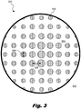
- Fig. 3 is a diagram showing an illustrative top view of a sub-wavelength grating element (300).
- a sub-wavelength grating element 300
- Such sub-wavelength grating elements may be used as described above (e.g. 214, 216, Fig. 2 ).
- the sub-wavelength grating element (300) is a two dimensional pattern formed into the grating layer (310).
- the grating layer (310) may be composed of a single elemental semiconductor such as silicon or germanium.
- the grating layer may be made of a compound semiconductor such as a III-V semiconductor.
- the Roman numerals III and V represent elements in the Ilia and Va columns of the Periodic Table of the Elements.
- the grating layer (310) is formed on top of the transparent layer.
- the grating layer (310) material is selected so that it has a higher refractive index than the underlying transparent layer. Due to this relatively high difference in refractive index between the grating layer and the transparent layer, the sub-wavelength grating element can be referred to as a high-contrast sub-wavelength grating element.
- the grating patterns can be formed into the grating layer (310) to form the sub-wavelength grating elements using Complementary Metal Oxide Semiconductor (CMOS) compatible techniques.
- CMOS Complementary Metal Oxide Semiconductor
- a sub-wavelength grating element (300) can be fabricated by depositing the grating layer (310) on a planar surface of the transparent layer using wafer bonding or chemical or physical vapor deposition. Photolithography techniques may then be used to remove portions of the grating layer (310) to expose the transparent layer (304) underneath. Removing portions of the grating layer (310) will leave a number of grating features (302).
- the grating features (302) are posts. However, in some cases, the grating features may be grooves.
- the distance between the centers of the grating features (302) is referred to as the lattice constant (308).
- the lattice constant (308) is selected so that the sub-wavelength grating element does not scatter light in an unwanted manner. Unwanted scattering can be prevented by selecting the lattice constant appropriately.
- the sub-wavelength grating may also be non-periodic. That is, the parameters of the grating features such as the diameter of the posts or the width of the grooves may vary across the area of the sub-wavelength grating element (300). Both the dimensions (306) of the grating features (302) and the length of the lattice constant (308) are less than the wavelength of light produced by the VCSELs that travels through the sub-wavelength grating element.
- the lattice constant (308) and grating feature parameters can be selected so that the sub-wavelength grating element (300) can be made to perform a specific function.
- the sub-wavelength grating element (300) may be designed to focus light in a particular manner.
- the sub-wavelength grating element (300) may be designed to collimate light.
- the sub-wavelength grating element may tilt the collimated beam at a specific angle.
- the sub-wavelength grating element may split or bend a beam of light. More detail about methods for designing such sub-wavelength grating elements for specific functions can be found at, for example, US Patent Publication No. 2011/0261856, published on Oct. 27, 2011 .
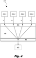
- Fig. 4 is a diagram showing an illustrative integrated sub-wavelength grating system used as a multiplexer (400).
- an optical multiplexer is used to combine different optical signals of different wavelength into the same optical transmission medium so that those signals can propagate simultaneously though the medium.
- multiple optical sources such as VCSELs are designed to project light of different wavelengths.
- the beams of light from those VCSELs (402) are projected toward an array (404) of sub-wavelength gratings.
- Each sub-wavelength grating within that array is specifically aligned and designed to direct the light from the corresponding VCSEL through a transparent medium (406) towards a single point.
- a diffraction grating from an array (408) of diffraction gratings will collect that light and direct it towards an optical transmission medium (410).
- Fig. 5 is a diagram showing an illustrative integrated sub-wavelength grating system used as a demultiplexer (500).
- an optical demultiplexer divides a beam of light according to wavelength.
- beams of light having different wavelength that were combined into a single optical transmission medium can then be separated for further processing.
- each separate beam of light reaches a sub-wavelength grating element of an array (506) of sub-wavelength grating elements. Those sub-wavelength grating elements then focus their respective beams of light towards an array of optoelectronic detector devices (508).
- the multiple wavelengths of light may be of a relative small difference.
- the difference in angle for each beam of light when passing through the diffracted grating may be relatively small.
- the transparent layer between the diffraction grating elements and the sub-wavelength grating elements may be relatively thick.
- this thickness may be undesirable. The following describes a method for using a relatively thin transparent layer even when the difference in wavelength between the discrete beams yields a relatively small angular spread.
- Fig. 6 is a diagram showing an illustrative integrated sub-wavelength grating system (600) with a thin transparent layer and reflective surfaces used to increase angular spread.
- a multi-wavelength beam of light (604) is projected from an optical transmission medium (602) to a diffraction grating element (606) formed within a second grating layer (608).
- the diffraction grating element (606) causes the multi-wavelength beam of light to be split according to wavelength. In this example, the split results in two beams of light (610, 612) of different wavelengths.
- the two beams (610, 612) are not spread far enough apart by the time they reach the first grating layer (618).
- a reflective element (614) is formed within the first grating layer (618) to reflect those beams of light back through the transparent layer (620).
- another reflective element (616) is formed within the second grating layer (608) to bounce the light beams back through the transparent layer (620) towards the first grating layer (618).
- the light beams (610, 612) may bounce back and forth several times before reaching the sub-wavelength grating elements (622, 624) formed within the first grating layer (618).
- each beam of light Upon reaching the sub-wavelength grating elements (622, 624) each beam of light will be properly redirected and focused toward a corresponding optoelectronic component.
- the first sub-wavelength grating (622) is designed to direct light from the angle at which the first beam (612) is received toward a first optoelectronic component (626).
- the second sub-wavelength grating (624) is designed to direct light from the angle at which the second beam (610) is received toward a second optoelectronic component (628).
- Various materials may be used to form the reflective elements.
- portions of the grating layer may be etched away and filled with a reflective layer.
- a reflective substance may be disposed on the transparent layer before the grating layer is disposed.
- no specific reflective elements are formed. Rather, the light bounces based on total internal reflection.
- Total internal reflection refers to the process whereby light strikes a medium boundary at an angle larger than a particular critical angle with respect to a vector normal to the surface. If the refractive index is lower on the other side of the boundary and the incident angle is greater than the critical angle, then all light will be reflected. In this case, if the material outside the boundary of the transparent layer has a lower refractive index than the transparent material, then light will be internally reflected as long as the incident angle is larger than the critical angle.
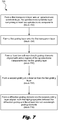
- Fig. 7 is a flowchart (700) showing an illustrative method for forming an integrated sub-wavelength grating system.
- the method includes forming (block 702) a first transparent layer onto an optoelectronic substrate layer, the optoelectronic substrate layer comprising at least two optoelectronic components, forming (block 704) a first grating layer onto the first transparent layer, forming (block 706) at least two sub-wavelength grating elements aligned with active regions of the optoelectronic components into the first grating layer, forming (block 708) a second grating at a distance from the first grating layer, and forming (block 710) a diffraction grating element into the second grating layer aligned such that light propagates between the diffraction grating and the at least two sub-wavelength grating elements.
- multiplexing and demultiplexing systems can be formed onto an integrated chip in a monolithic manner.
- no use of complicated lens systems and alignment processes are used.
- Such systems allow for less costly and more compact optical transmission systems.
Claims (15)
- Système d'éléments de réseau intégré (200) comprenant :une couche de substrat optoélectronique (226) comprenant au moins deux composants optoélectroniques (224-1 ; 224-2) ;une première couche transparente (222) formée sur ladite couche de substrat optoélectronique ;une première couche de réseau (212) disposée sur ladite première couche transparente et ayant un indice de réfraction supérieur à celui de la première couche transparente, ladite couche de réseau comprenant au moins deux éléments de réseau à sous-longueur d'onde (214, 216) formés dans celle-ci alignés avec des régions actives desdits composants optoélectroniques ; etune seconde couche de réseau (204) à une distance de ladite première couche de réseau de telle sorte que de la lumière se propage entre un élément de réseau de diffraction (206) formé à l'intérieur de ladite seconde couche de réseau et desdits au moins deux éléments de réseau à sous-longueur d'onde,dans lequel les au moins deux composants optoélectroniques comprennent des sources optiques et le système fonctionne comme un multiplexeur, ou les au moins deux composants optoélectroniques comprennent des détecteurs optiques et le système fonctionne comme un démultiplexeur.
- Système selon la revendication 1, dans lequel ladite distance entre ladite première couche de réseau et ladite seconde couche de réseau comprend une seconde couche transparente (208).
- Système selon la revendication 1, comprenant en outre des surfaces réfléchissantes positionnées pour faire rebondir de la lumière entre ladite première couche de réseau et ladite seconde couche de réseau entre ledit élément de réseau de diffraction et lesdits éléments de réseau à sous-longueur d'onde.
- Système selon la revendication 1, dans lequel lesdits au moins deux composants optoélectroniques comprennent des sources optiques pour projeter de la lumière de différentes longueurs d'onde dans lesdits éléments de réseau à sous-longueur d'onde.
- Système selon la revendication 4, dans lequel lesdits éléments de réseau à sous-longueur d'onde sont destinés à collimater et orienter de la lumière projetée provenant desdites sources optiques vers ledit élément de réseau de diffraction formé à l'intérieur de ladite seconde couche de réseau.
- Système selon la revendication 1, dans lequel lesdits au moins deux composants optoélectroniques comprennent des dispositifs de détection optique pour recevoir de la lumière de différentes longueurs d'onde provenant desdits éléments de réseau à sous-longueur d'onde.
- Système selon la revendication 6, dans lequel lesdits éléments de réseau de diffraction sont destinés à diviser de la lumière incidente en de multiples directions selon la longueur d'onde, lesdites directions pointant vers lesdits éléments de réseau à sous-longueur d'onde.
- Système selon la revendication 1, dans lequel lesdits éléments de réseau à sous-longueur d'onde comprennent des variations bidimensionnelles non périodiques de paramètres de caractéristique de réseau pour affecter de la lumière d'une manière prédéterminée.
- Procédé (700) pour former un système de réseau à sous-longueur d'onde intégré, le procédé comprenant :la formation (702) d'une première couche transparente sur une couche de substrat optoélectronique, ladite couche de substrat optoélectronique comprenant au moins deux composants optoélectroniques ;la formation (704) d'une première couche de réseau sur ladite première couche transparente ayant un indice de réfraction supérieur à celui de la première couche transparente ;la formation (706) d'au moins deux éléments de réseau à sous-longueur d'onde alignés avec des régions actives desdits composants optoélectroniques dans ladite première couche de réseau ;la formation (708) d'un second réseau à distance de ladite première couche de réseau ; etla formation (710) d'un élément de réseau de diffraction dans ladite seconde couche de réseau aligné de telle sorte que de la lumière se propage entre ledit réseau de diffraction et lesdits au moins deux éléments de réseau à sous-longueur d'onde.
- Procédé selon la revendication 9, comprenant en outre la réflexion de lumière entre ladite première couche de réseau et ladite seconde couche de réseau entre ledit élément de réseau de diffraction et lesdits éléments de réseau à sous-longueur d'onde.
- Procédé selon la revendication 9, dans lequel lesdits au moins deux composants optoélectroniques comprennent des sources optiques pour projeter de la lumière de différentes longueurs d'onde dans lesdits éléments de réseau à sous-longueur d'onde.
- Procédé selon la revendication 11, comprenant en outre, avec lesdits éléments de réseau à sous-longueur d'onde, la collimation et l'inclinaison de lumière provenant desdites sources optiques vers ledit élément de réseau de diffraction.
- Procédé selon la revendication 9, dans lequel lesdits au moins deux composants optoélectroniques comprennent des dispositifs de détection optique pour recevoir de la lumière de différentes longueurs d'onde provenant desdits éléments de réseau à sous-longueur d'onde.
- Procédé selon la revendication 13, comprenant en outre, avec ledit élément de réseau de diffraction, la division de lumière incidente en de multiples directions selon la longueur d'onde, lesdites directions pointant vers lesdits éléments de réseau à sous-longueur d'onde.
- Puce de circuit intégré comprenant le système d'éléments de réseau intégré selon la revendication 1, comprenant :
une seconde couche transparente formée sur ladite première couche de réseau, dans laquelle :ladite couche de substrat optoélectronique comprend un réseau de composants optoélectroniques ;ladite première couche de réseau comprend un réseau de deux éléments de réseau à sous-longueur d'onde formés dans celle-ci alignés avec des régions actives desdits composants optoélectroniques ;ladite seconde couche de réseau est formée sur ladite seconde couche transparente ; etladite seconde couche de réseau comprend un réseau d'éléments de réseau de diffraction, chaque élément de réseau de diffraction étant configuré pour coupler de la lumière entre au moins deux desdits éléments de réseau à sous-longueur d'onde à des longueurs d'onde différentes.
Applications Claiming Priority (1)
| Application Number | Priority Date | Filing Date | Title |
|---|---|---|---|
| PCT/US2012/021066 WO2013105959A1 (fr) | 2012-01-12 | 2012-01-12 | Système de réseau à sous-longueur d'onde intégré |
Publications (3)
| Publication Number | Publication Date |
|---|---|
| EP2803123A1 EP2803123A1 (fr) | 2014-11-19 |
| EP2803123A4 EP2803123A4 (fr) | 2015-09-23 |
| EP2803123B1 true EP2803123B1 (fr) | 2020-11-25 |
Family
ID=48781764
Family Applications (1)
| Application Number | Title | Priority Date | Filing Date |
|---|---|---|---|
| EP12864761.7A Active EP2803123B1 (fr) | 2012-01-12 | 2012-01-12 | Système de réseau à sous-longueur d'onde intégré |
Country Status (5)
| Country | Link |
|---|---|
| US (1) | US9612402B2 (fr) |
| EP (1) | EP2803123B1 (fr) |
| KR (1) | KR20140112012A (fr) |
| CN (1) | CN103999303B (fr) |
| WO (1) | WO2013105959A1 (fr) |
Families Citing this family (16)
| Publication number | Priority date | Publication date | Assignee | Title |
|---|---|---|---|---|
| WO2013109265A1 (fr) * | 2012-01-18 | 2013-07-25 | Hewlett-Packard Development Company, L.P. | Élément intégré de réseau sous-longueur d'onde |
| CN105075152A (zh) * | 2013-04-11 | 2015-11-18 | 惠普发展公司,有限责任合伙企业 | 用于光隔离的模式转换 |
| EP2999980B1 (fr) | 2013-05-22 | 2021-09-29 | Hewlett Packard Enterprise Development LP | Dispositifs optiques comprenant une lentille à réseau à grand contraste |
| WO2015065344A1 (fr) * | 2013-10-29 | 2015-05-07 | Hewlett-Packard Development Company, L.P. | Optoélectronique à réseau de diffraction à contraste élevé |
| WO2015112166A1 (fr) | 2014-01-24 | 2015-07-30 | Hewlett-Packard Development Company, L.P. | Dispositif de modulation optique mettant en œuvre une lentille à réseau haut contraste |
| CN106129789B (zh) * | 2016-08-31 | 2019-03-12 | 南方科技大学 | 光纤激光器 |
| CN110710072B (zh) * | 2017-04-12 | 2022-07-22 | 感应光子公司 | 具有结合光束转向的超小型垂直腔表面发射激光发射器的器件 |
| FR3077652B1 (fr) * | 2018-02-05 | 2022-05-27 | Commissariat Energie Atomique | Puce photonique a structure de collimation integree |
| WO2019207438A1 (fr) * | 2018-04-26 | 2019-10-31 | SM Optics S.r.l. | Dispositif optique destiné à démultiplexer et multiplexer des modes avec un moment angulaire orbital différent |
| CN110764186B (zh) * | 2018-07-27 | 2022-02-22 | 京东方科技集团股份有限公司 | 光波导基板和微流控装置 |
| US11344882B2 (en) | 2018-07-26 | 2022-05-31 | Boe Technology Group Co., Ltd. | Microfluidic apparatus, and method of detecting substance in microfluidic apparatus |
| CN109038216B (zh) * | 2018-10-29 | 2023-10-31 | 厦门乾照半导体科技有限公司 | 一种多光束垂直腔面发射激光芯片及其制作方法 |
| US10795098B2 (en) * | 2018-12-21 | 2020-10-06 | Hewlett Packard Enterprise Development Lp | Mode division multiplexing using vertical-cavity surface emitting lasers |
| US20210132196A1 (en) * | 2019-11-06 | 2021-05-06 | Lookit.ai | Flat optics with passive elements functioning as a transformation optics and a compact scanner to cover the vertical elevation field-of-view |
| CN115210619A (zh) * | 2020-01-31 | 2022-10-18 | 康宁股份有限公司 | 用于光纤通信的使用超材料的波长复用器/解复用器 |
| CN115201970B (zh) * | 2022-07-13 | 2023-10-20 | 北京摩尔芯光半导体技术有限公司 | 具有光栅耦合器的硅基光学芯片 |
Citations (1)
| Publication number | Priority date | Publication date | Assignee | Title |
|---|---|---|---|---|
| US4994664A (en) * | 1989-03-27 | 1991-02-19 | Massachusetts Institute Of Technology | Optically coupled focal plane arrays using lenslets and multiplexers |
Family Cites Families (22)
| Publication number | Priority date | Publication date | Assignee | Title |
|---|---|---|---|---|
| US4944664A (en) * | 1989-09-19 | 1990-07-31 | Allred Cecil F | Concrete wall form apparatus |
| US5061027A (en) * | 1990-09-04 | 1991-10-29 | Motorola, Inc. | Solder-bump attached optical interconnect structure utilizing holographic elements and method of making same |
| JPH08507879A (ja) * | 1993-02-26 | 1996-08-20 | イエダ リサーチ アンド デベロツプメント カンパニー リミテツド | ホログラフィー光学装置 |
| JP3119540B2 (ja) | 1993-04-12 | 2000-12-25 | 松下電器産業株式会社 | 光タップ |
| US5731874A (en) * | 1995-01-24 | 1998-03-24 | The Board Of Trustees Of The Leland Stanford Junior University | Discrete wavelength spectrometer |
| US20030002789A1 (en) * | 2000-10-31 | 2003-01-02 | Boye Robert R. | Integrated optical coupler |
| US6490393B1 (en) * | 2000-11-27 | 2002-12-03 | Advanced Interfaces, Llc | Integrated optical multiplexer and demultiplexer for wavelength division transmission of information |
| US7050675B2 (en) | 2000-11-27 | 2006-05-23 | Advanced Interfaces, Llc | Integrated optical multiplexer and demultiplexer for wavelength division transmission of information |
| US6782027B2 (en) | 2000-12-29 | 2004-08-24 | Finisar Corporation | Resonant reflector for use with optoelectronic devices |
| US7177496B1 (en) | 2001-12-27 | 2007-02-13 | Capella Photonics, Inc. | Optical spectral power monitors employing time-division-multiplexing detection schemes |
| JP3949977B2 (ja) * | 2002-02-18 | 2007-07-25 | 沖電気工業株式会社 | 波長分割多重通信用光分波器 |
| WO2004027493A1 (fr) | 2002-09-20 | 2004-04-01 | Nippon Sheet Glass Company, Limited | Spectrometre a reseau diffracteur |
| JP2004226901A (ja) | 2003-01-27 | 2004-08-12 | Ricoh Co Ltd | 波長合分波器及びその製造方法 |
| JP4425059B2 (ja) * | 2003-06-25 | 2010-03-03 | シャープ株式会社 | 偏光光学素子、およびそれを用いた表示装置 |
| EP1691224A1 (fr) | 2005-02-10 | 2006-08-16 | Konica Minolta Opto, Inc. | Élément de réseau à diffraction et module de communication optique |
| US7460231B2 (en) | 2006-03-27 | 2008-12-02 | Asml Netherlands B.V. | Alignment tool for a lithographic apparatus |
| TWI354809B (en) | 2008-06-24 | 2011-12-21 | Ind Tech Res Inst | Composite optical dividing device |
| US8400537B2 (en) * | 2008-11-13 | 2013-03-19 | Omnivision Technologies, Inc. | Image sensors having gratings for color separation |
| WO2010140998A1 (fr) | 2009-06-02 | 2010-12-09 | Vladimir Yankov | Nanospectromètre intégré optique et procédé de fabrication de celui-ci |
| US9229138B2 (en) | 2009-10-06 | 2016-01-05 | Sri International | Twin sub-wavelength grating optical signal processor |
| WO2011106553A2 (fr) * | 2010-02-24 | 2011-09-01 | The Regents Of The University Of California | Lentilles de réflexion ou de transmission planes à faible perte, à ouverture numérique élevée, comprenant des réseaux à contraste élevé sub-longueur d'onde |
| CN102073103B (zh) * | 2010-11-22 | 2013-11-13 | 北京交通大学 | 基于亚波长二元衍射光栅的波长分离器 |
-
2012
- 2012-01-12 US US14/364,702 patent/US9612402B2/en active Active
- 2012-01-12 EP EP12864761.7A patent/EP2803123B1/fr active Active
- 2012-01-12 KR KR1020147015966A patent/KR20140112012A/ko not_active Application Discontinuation
- 2012-01-12 CN CN201280061237.XA patent/CN103999303B/zh active Active
- 2012-01-12 WO PCT/US2012/021066 patent/WO2013105959A1/fr active Application Filing
Patent Citations (1)
| Publication number | Priority date | Publication date | Assignee | Title |
|---|---|---|---|---|
| US4994664A (en) * | 1989-03-27 | 1991-02-19 | Massachusetts Institute Of Technology | Optically coupled focal plane arrays using lenslets and multiplexers |
Also Published As
| Publication number | Publication date |
|---|---|
| KR20140112012A (ko) | 2014-09-22 |
| CN103999303A (zh) | 2014-08-20 |
| CN103999303B (zh) | 2018-03-13 |
| EP2803123A4 (fr) | 2015-09-23 |
| EP2803123A1 (fr) | 2014-11-19 |
| WO2013105959A1 (fr) | 2013-07-18 |
| US20150010271A1 (en) | 2015-01-08 |
| US9612402B2 (en) | 2017-04-04 |
Similar Documents
| Publication | Publication Date | Title |
|---|---|---|
| EP2803123B1 (fr) | Système de réseau à sous-longueur d'onde intégré | |
| US9817193B2 (en) | Through-substrate optical coupling to photonics chips | |
| US7376308B2 (en) | Optical off-chip interconnects in multichannel planar waveguide devices | |
| JP4789619B2 (ja) | 光学装置および光学装置を組み込んだ光学アセンブリ | |
| US9482816B2 (en) | Radiation coupler | |
| EP2626731B1 (fr) | Agencement de couplage optique | |
| JP2019168673A (ja) | コリメーション構造体が集積されたフォトニックチップ | |
| KR101420623B1 (ko) | 광 도파로와, 다른 광 도파로, 부품 또는 디바이스 간의 자유 공간 전파를 위한 광학 소자 | |
| US9077450B2 (en) | Wavelength division multiplexing with multi-core fiber | |
| US7561764B2 (en) | Integrated reflector for planar lightwave circuits | |
| US20140321495A1 (en) | Integrated sub-wavelength grating element | |
| US20160327746A1 (en) | Bidirectional optical multiplexing employing a high contrast grating | |
| KR20140082853A (ko) | 광학 연결부 | |
| JP5983479B2 (ja) | 光素子 | |
| US7277611B1 (en) | Optical interconnect platform including Bragg diffractive gratings in a bulk material | |
| JP2003066269A (ja) | 波長多重分離光学デバイス及び波長多重光伝送モジュール | |
| JP2010506201A (ja) | 反射格子を有するハイブリッド・プレーナ型光波回路 | |
| EP3995872A1 (fr) | Couplage optique de faisceau étendu à deux étages | |
| KR20100074704A (ko) | 다파장 분리용 광모듈 | |
| JP2005249966A (ja) | 光学部材とその製造方法,光モジュール | |
| JP2002169054A (ja) | 波長合分波器 | |
| JP4696521B2 (ja) | デマルチプレクサ、光導波路、及び波長多重光伝送モジュール | |
| JP2004070322A (ja) | 波長分波器 | |
| JP2005134572A (ja) | 光導波回路 |
Legal Events
| Date | Code | Title | Description |
|---|---|---|---|
| PUAI | Public reference made under article 153(3) epc to a published international application that has entered the european phase |
Free format text: ORIGINAL CODE: 0009012 |
|
| 17P | Request for examination filed |
Effective date: 20140519 |
|
| AK | Designated contracting states |
Kind code of ref document: A1 Designated state(s): AL AT BE BG CH CY CZ DE DK EE ES FI FR GB GR HR HU IE IS IT LI LT LU LV MC MK MT NL NO PL PT RO RS SE SI SK SM TR |
|
| DAX | Request for extension of the european patent (deleted) | ||
| RA4 | Supplementary search report drawn up and despatched (corrected) |
Effective date: 20150821 |
|
| RIC1 | Information provided on ipc code assigned before grant |
Ipc: H01L 31/0248 20060101ALI20150817BHEP Ipc: G02B 6/293 20060101ALI20150817BHEP Ipc: H01S 5/183 20060101AFI20150817BHEP |
|
| RAP1 | Party data changed (applicant data changed or rights of an application transferred) |
Owner name: HEWLETT PACKARD ENTERPRISE DEVELOPMENT L.P. |
|
| STAA | Information on the status of an ep patent application or granted ep patent |
Free format text: STATUS: EXAMINATION IS IN PROGRESS |
|
| 17Q | First examination report despatched |
Effective date: 20181130 |
|
| REG | Reference to a national code |
Ref country code: DE Ref legal event code: R079 Ref document number: 602012073434 Country of ref document: DE Free format text: PREVIOUS MAIN CLASS: H01S0005183000 Ipc: G02B0006293000 |
|
| GRAP | Despatch of communication of intention to grant a patent |
Free format text: ORIGINAL CODE: EPIDOSNIGR1 |
|
| STAA | Information on the status of an ep patent application or granted ep patent |
Free format text: STATUS: GRANT OF PATENT IS INTENDED |
|
| RIC1 | Information provided on ipc code assigned before grant |
Ipc: G02B 6/293 20060101AFI20200519BHEP |
|
| INTG | Intention to grant announced |
Effective date: 20200617 |
|
| GRAS | Grant fee paid |
Free format text: ORIGINAL CODE: EPIDOSNIGR3 |
|
| GRAA | (expected) grant |
Free format text: ORIGINAL CODE: 0009210 |
|
| STAA | Information on the status of an ep patent application or granted ep patent |
Free format text: STATUS: THE PATENT HAS BEEN GRANTED |
|
| AK | Designated contracting states |
Kind code of ref document: B1 Designated state(s): AL AT BE BG CH CY CZ DE DK EE ES FI FR GB GR HR HU IE IS IT LI LT LU LV MC MK MT NL NO PL PT RO RS SE SI SK SM TR |
|
| REG | Reference to a national code |
Ref country code: GB Ref legal event code: FG4D |
|
| REG | Reference to a national code |
Ref country code: CH Ref legal event code: EP |
|
| REG | Reference to a national code |
Ref country code: DE Ref legal event code: R096 Ref document number: 602012073434 Country of ref document: DE |
|
| REG | Reference to a national code |
Ref country code: AT Ref legal event code: REF Ref document number: 1338973 Country of ref document: AT Kind code of ref document: T Effective date: 20201215 |
|
| REG | Reference to a national code |
Ref country code: IE Ref legal event code: FG4D |
|
| REG | Reference to a national code |
Ref country code: AT Ref legal event code: MK05 Ref document number: 1338973 Country of ref document: AT Kind code of ref document: T Effective date: 20201125 |
|
| REG | Reference to a national code |
Ref country code: NL Ref legal event code: MP Effective date: 20201125 |
|
| PG25 | Lapsed in a contracting state [announced via postgrant information from national office to epo] |
Ref country code: GR Free format text: LAPSE BECAUSE OF FAILURE TO SUBMIT A TRANSLATION OF THE DESCRIPTION OR TO PAY THE FEE WITHIN THE PRESCRIBED TIME-LIMIT Effective date: 20210226 Ref country code: FI Free format text: LAPSE BECAUSE OF FAILURE TO SUBMIT A TRANSLATION OF THE DESCRIPTION OR TO PAY THE FEE WITHIN THE PRESCRIBED TIME-LIMIT Effective date: 20201125 Ref country code: RS Free format text: LAPSE BECAUSE OF FAILURE TO SUBMIT A TRANSLATION OF THE DESCRIPTION OR TO PAY THE FEE WITHIN THE PRESCRIBED TIME-LIMIT Effective date: 20201125 Ref country code: NO Free format text: LAPSE BECAUSE OF FAILURE TO SUBMIT A TRANSLATION OF THE DESCRIPTION OR TO PAY THE FEE WITHIN THE PRESCRIBED TIME-LIMIT Effective date: 20210225 Ref country code: PT Free format text: LAPSE BECAUSE OF FAILURE TO SUBMIT A TRANSLATION OF THE DESCRIPTION OR TO PAY THE FEE WITHIN THE PRESCRIBED TIME-LIMIT Effective date: 20210325 |
|
| PG25 | Lapsed in a contracting state [announced via postgrant information from national office to epo] |
Ref country code: AT Free format text: LAPSE BECAUSE OF FAILURE TO SUBMIT A TRANSLATION OF THE DESCRIPTION OR TO PAY THE FEE WITHIN THE PRESCRIBED TIME-LIMIT Effective date: 20201125 Ref country code: BG Free format text: LAPSE BECAUSE OF FAILURE TO SUBMIT A TRANSLATION OF THE DESCRIPTION OR TO PAY THE FEE WITHIN THE PRESCRIBED TIME-LIMIT Effective date: 20210225 Ref country code: SE Free format text: LAPSE BECAUSE OF FAILURE TO SUBMIT A TRANSLATION OF THE DESCRIPTION OR TO PAY THE FEE WITHIN THE PRESCRIBED TIME-LIMIT Effective date: 20201125 Ref country code: IS Free format text: LAPSE BECAUSE OF FAILURE TO SUBMIT A TRANSLATION OF THE DESCRIPTION OR TO PAY THE FEE WITHIN THE PRESCRIBED TIME-LIMIT Effective date: 20210325 Ref country code: LV Free format text: LAPSE BECAUSE OF FAILURE TO SUBMIT A TRANSLATION OF THE DESCRIPTION OR TO PAY THE FEE WITHIN THE PRESCRIBED TIME-LIMIT Effective date: 20201125 Ref country code: PL Free format text: LAPSE BECAUSE OF FAILURE TO SUBMIT A TRANSLATION OF THE DESCRIPTION OR TO PAY THE FEE WITHIN THE PRESCRIBED TIME-LIMIT Effective date: 20201125 |
|
| REG | Reference to a national code |
Ref country code: LT Ref legal event code: MG9D |
|
| PG25 | Lapsed in a contracting state [announced via postgrant information from national office to epo] |
Ref country code: HR Free format text: LAPSE BECAUSE OF FAILURE TO SUBMIT A TRANSLATION OF THE DESCRIPTION OR TO PAY THE FEE WITHIN THE PRESCRIBED TIME-LIMIT Effective date: 20201125 |
|
| PG25 | Lapsed in a contracting state [announced via postgrant information from national office to epo] |
Ref country code: CZ Free format text: LAPSE BECAUSE OF FAILURE TO SUBMIT A TRANSLATION OF THE DESCRIPTION OR TO PAY THE FEE WITHIN THE PRESCRIBED TIME-LIMIT Effective date: 20201125 Ref country code: EE Free format text: LAPSE BECAUSE OF FAILURE TO SUBMIT A TRANSLATION OF THE DESCRIPTION OR TO PAY THE FEE WITHIN THE PRESCRIBED TIME-LIMIT Effective date: 20201125 Ref country code: SM Free format text: LAPSE BECAUSE OF FAILURE TO SUBMIT A TRANSLATION OF THE DESCRIPTION OR TO PAY THE FEE WITHIN THE PRESCRIBED TIME-LIMIT Effective date: 20201125 Ref country code: SK Free format text: LAPSE BECAUSE OF FAILURE TO SUBMIT A TRANSLATION OF THE DESCRIPTION OR TO PAY THE FEE WITHIN THE PRESCRIBED TIME-LIMIT Effective date: 20201125 Ref country code: RO Free format text: LAPSE BECAUSE OF FAILURE TO SUBMIT A TRANSLATION OF THE DESCRIPTION OR TO PAY THE FEE WITHIN THE PRESCRIBED TIME-LIMIT Effective date: 20201125 Ref country code: LT Free format text: LAPSE BECAUSE OF FAILURE TO SUBMIT A TRANSLATION OF THE DESCRIPTION OR TO PAY THE FEE WITHIN THE PRESCRIBED TIME-LIMIT Effective date: 20201125 |
|
| REG | Reference to a national code |
Ref country code: DE Ref legal event code: R097 Ref document number: 602012073434 Country of ref document: DE |
|
| PG25 | Lapsed in a contracting state [announced via postgrant information from national office to epo] |
Ref country code: MC Free format text: LAPSE BECAUSE OF FAILURE TO SUBMIT A TRANSLATION OF THE DESCRIPTION OR TO PAY THE FEE WITHIN THE PRESCRIBED TIME-LIMIT Effective date: 20201125 Ref country code: DK Free format text: LAPSE BECAUSE OF FAILURE TO SUBMIT A TRANSLATION OF THE DESCRIPTION OR TO PAY THE FEE WITHIN THE PRESCRIBED TIME-LIMIT Effective date: 20201125 |
|
| REG | Reference to a national code |
Ref country code: CH Ref legal event code: PL |
|
| PG25 | Lapsed in a contracting state [announced via postgrant information from national office to epo] |
Ref country code: LU Free format text: LAPSE BECAUSE OF NON-PAYMENT OF DUE FEES Effective date: 20210112 |
|
| PLBE | No opposition filed within time limit |
Free format text: ORIGINAL CODE: 0009261 |
|
| STAA | Information on the status of an ep patent application or granted ep patent |
Free format text: STATUS: NO OPPOSITION FILED WITHIN TIME LIMIT |
|
| REG | Reference to a national code |
Ref country code: BE Ref legal event code: MM Effective date: 20210131 |
|
| GBPC | Gb: european patent ceased through non-payment of renewal fee |
Effective date: 20210225 |
|
| PG25 | Lapsed in a contracting state [announced via postgrant information from national office to epo] |
Ref country code: FR Free format text: LAPSE BECAUSE OF NON-PAYMENT OF DUE FEES Effective date: 20210125 Ref country code: NL Free format text: LAPSE BECAUSE OF FAILURE TO SUBMIT A TRANSLATION OF THE DESCRIPTION OR TO PAY THE FEE WITHIN THE PRESCRIBED TIME-LIMIT Effective date: 20201125 Ref country code: AL Free format text: LAPSE BECAUSE OF FAILURE TO SUBMIT A TRANSLATION OF THE DESCRIPTION OR TO PAY THE FEE WITHIN THE PRESCRIBED TIME-LIMIT Effective date: 20201125 Ref country code: IT Free format text: LAPSE BECAUSE OF FAILURE TO SUBMIT A TRANSLATION OF THE DESCRIPTION OR TO PAY THE FEE WITHIN THE PRESCRIBED TIME-LIMIT Effective date: 20201125 |
|
| 26N | No opposition filed |
Effective date: 20210826 |
|
| PG25 | Lapsed in a contracting state [announced via postgrant information from national office to epo] |
Ref country code: SI Free format text: LAPSE BECAUSE OF FAILURE TO SUBMIT A TRANSLATION OF THE DESCRIPTION OR TO PAY THE FEE WITHIN THE PRESCRIBED TIME-LIMIT Effective date: 20201125 Ref country code: LI Free format text: LAPSE BECAUSE OF NON-PAYMENT OF DUE FEES Effective date: 20210131 Ref country code: CH Free format text: LAPSE BECAUSE OF NON-PAYMENT OF DUE FEES Effective date: 20210131 |
|
| PG25 | Lapsed in a contracting state [announced via postgrant information from national office to epo] |
Ref country code: IE Free format text: LAPSE BECAUSE OF NON-PAYMENT OF DUE FEES Effective date: 20210112 Ref country code: GB Free format text: LAPSE BECAUSE OF NON-PAYMENT OF DUE FEES Effective date: 20210225 |
|
| PG25 | Lapsed in a contracting state [announced via postgrant information from national office to epo] |
Ref country code: IS Free format text: LAPSE BECAUSE OF FAILURE TO SUBMIT A TRANSLATION OF THE DESCRIPTION OR TO PAY THE FEE WITHIN THE PRESCRIBED TIME-LIMIT Effective date: 20210325 |
|
| PG25 | Lapsed in a contracting state [announced via postgrant information from national office to epo] |
Ref country code: BE Free format text: LAPSE BECAUSE OF NON-PAYMENT OF DUE FEES Effective date: 20210131 |
|
| REG | Reference to a national code |
Ref country code: DE Ref legal event code: R082 Ref document number: 602012073434 Country of ref document: DE Representative=s name: FLEUCHAUS & GALLO PARTNERSCHAFT MBB - PATENT- , DE Ref country code: DE Ref legal event code: R082 Ref document number: 602012073434 Country of ref document: DE Representative=s name: FLEUCHAUS & GALLO PARTNERSCHAFT MBB PATENTANWA, DE |
|
| PG25 | Lapsed in a contracting state [announced via postgrant information from national office to epo] |
Ref country code: HU Free format text: LAPSE BECAUSE OF FAILURE TO SUBMIT A TRANSLATION OF THE DESCRIPTION OR TO PAY THE FEE WITHIN THE PRESCRIBED TIME-LIMIT; INVALID AB INITIO Effective date: 20120112 Ref country code: CY Free format text: LAPSE BECAUSE OF FAILURE TO SUBMIT A TRANSLATION OF THE DESCRIPTION OR TO PAY THE FEE WITHIN THE PRESCRIBED TIME-LIMIT Effective date: 20201125 |
|
| PG25 | Lapsed in a contracting state [announced via postgrant information from national office to epo] |
Ref country code: ES Free format text: LAPSE BECAUSE OF FAILURE TO SUBMIT A TRANSLATION OF THE DESCRIPTION OR TO PAY THE FEE WITHIN THE PRESCRIBED TIME-LIMIT Effective date: 20201125 |
|
| PG25 | Lapsed in a contracting state [announced via postgrant information from national office to epo] |
Ref country code: MK Free format text: LAPSE BECAUSE OF FAILURE TO SUBMIT A TRANSLATION OF THE DESCRIPTION OR TO PAY THE FEE WITHIN THE PRESCRIBED TIME-LIMIT Effective date: 20201125 |
|
| PGFP | Annual fee paid to national office [announced via postgrant information from national office to epo] |
Ref country code: DE Payment date: 20240129 Year of fee payment: 13 |