EP2793074A2 - Écran couleur à cristaux liquides, son procédé de fabrication et dispositif d'affichage couleur à cristaux liquides l'utilisant - Google Patents
Écran couleur à cristaux liquides, son procédé de fabrication et dispositif d'affichage couleur à cristaux liquides l'utilisant Download PDFInfo
- Publication number
- EP2793074A2 EP2793074A2 EP20140002491 EP14002491A EP2793074A2 EP 2793074 A2 EP2793074 A2 EP 2793074A2 EP 20140002491 EP20140002491 EP 20140002491 EP 14002491 A EP14002491 A EP 14002491A EP 2793074 A2 EP2793074 A2 EP 2793074A2
- Authority
- EP
- European Patent Office
- Prior art keywords
- liquid crystal
- color
- color filter
- crystal panel
- transparent
- Prior art date
- Legal status (The legal status is an assumption and is not a legal conclusion. Google has not performed a legal analysis and makes no representation as to the accuracy of the status listed.)
- Withdrawn
Links
Images


Classifications
-
- G—PHYSICS
- G02—OPTICS
- G02F—OPTICAL DEVICES OR ARRANGEMENTS FOR THE CONTROL OF LIGHT BY MODIFICATION OF THE OPTICAL PROPERTIES OF THE MEDIA OF THE ELEMENTS INVOLVED THEREIN; NON-LINEAR OPTICS; FREQUENCY-CHANGING OF LIGHT; OPTICAL LOGIC ELEMENTS; OPTICAL ANALOGUE/DIGITAL CONVERTERS
- G02F1/00—Devices or arrangements for the control of the intensity, colour, phase, polarisation or direction of light arriving from an independent light source, e.g. switching, gating or modulating; Non-linear optics
- G02F1/01—Devices or arrangements for the control of the intensity, colour, phase, polarisation or direction of light arriving from an independent light source, e.g. switching, gating or modulating; Non-linear optics for the control of the intensity, phase, polarisation or colour
- G02F1/13—Devices or arrangements for the control of the intensity, colour, phase, polarisation or direction of light arriving from an independent light source, e.g. switching, gating or modulating; Non-linear optics for the control of the intensity, phase, polarisation or colour based on liquid crystals, e.g. single liquid crystal display cells
- G02F1/133—Constructional arrangements; Operation of liquid crystal cells; Circuit arrangements
- G02F1/1333—Constructional arrangements; Manufacturing methods
- G02F1/1335—Structural association of cells with optical devices, e.g. polarisers or reflectors
- G02F1/133509—Filters, e.g. light shielding masks
- G02F1/133514—Colour filters
- G02F1/133516—Methods for their manufacture, e.g. printing, electro-deposition or photolithography
-
- G—PHYSICS
- G02—OPTICS
- G02F—OPTICAL DEVICES OR ARRANGEMENTS FOR THE CONTROL OF LIGHT BY MODIFICATION OF THE OPTICAL PROPERTIES OF THE MEDIA OF THE ELEMENTS INVOLVED THEREIN; NON-LINEAR OPTICS; FREQUENCY-CHANGING OF LIGHT; OPTICAL LOGIC ELEMENTS; OPTICAL ANALOGUE/DIGITAL CONVERTERS
- G02F1/00—Devices or arrangements for the control of the intensity, colour, phase, polarisation or direction of light arriving from an independent light source, e.g. switching, gating or modulating; Non-linear optics
- G02F1/01—Devices or arrangements for the control of the intensity, colour, phase, polarisation or direction of light arriving from an independent light source, e.g. switching, gating or modulating; Non-linear optics for the control of the intensity, phase, polarisation or colour
- G02F1/13—Devices or arrangements for the control of the intensity, colour, phase, polarisation or direction of light arriving from an independent light source, e.g. switching, gating or modulating; Non-linear optics for the control of the intensity, phase, polarisation or colour based on liquid crystals, e.g. single liquid crystal display cells
- G02F1/133—Constructional arrangements; Operation of liquid crystal cells; Circuit arrangements
- G02F1/1333—Constructional arrangements; Manufacturing methods
- G02F1/1335—Structural association of cells with optical devices, e.g. polarisers or reflectors
- G02F1/133509—Filters, e.g. light shielding masks
- G02F1/133514—Colour filters
-
- G—PHYSICS
- G02—OPTICS
- G02F—OPTICAL DEVICES OR ARRANGEMENTS FOR THE CONTROL OF LIGHT BY MODIFICATION OF THE OPTICAL PROPERTIES OF THE MEDIA OF THE ELEMENTS INVOLVED THEREIN; NON-LINEAR OPTICS; FREQUENCY-CHANGING OF LIGHT; OPTICAL LOGIC ELEMENTS; OPTICAL ANALOGUE/DIGITAL CONVERTERS
- G02F1/00—Devices or arrangements for the control of the intensity, colour, phase, polarisation or direction of light arriving from an independent light source, e.g. switching, gating or modulating; Non-linear optics
- G02F1/01—Devices or arrangements for the control of the intensity, colour, phase, polarisation or direction of light arriving from an independent light source, e.g. switching, gating or modulating; Non-linear optics for the control of the intensity, phase, polarisation or colour
- G02F1/13—Devices or arrangements for the control of the intensity, colour, phase, polarisation or direction of light arriving from an independent light source, e.g. switching, gating or modulating; Non-linear optics for the control of the intensity, phase, polarisation or colour based on liquid crystals, e.g. single liquid crystal display cells
- G02F1/133—Constructional arrangements; Operation of liquid crystal cells; Circuit arrangements
- G02F1/1333—Constructional arrangements; Manufacturing methods
- G02F1/1335—Structural association of cells with optical devices, e.g. polarisers or reflectors
- G02F1/133553—Reflecting elements
- G02F1/133555—Transflectors
Definitions
- the present invention relates to a color liquid crystal panel suitably used as a display of a portable telephone, a method for manufacturing the same, and further a color liquid crystal display device employing the same, more particularly, to a color liquid crystal panel having an enhanced capability of displaying high quality images, a method for manufacturing the same, and further a color liquid crystal display device employing the same.
- a semi-transmissive liquid crystal display device consisting of a plurality of pixels, each having a transmissive display section and a reflective display section therein, has been developed as a liquid crystal display device equipped with both features of a transmissive liquid crystal display device and a reflective liquid crystal display device.
- a color filter for a transmissive display section and a color filter for a reflective display section are provided corresponding to each color to be displayed and therefore, totally six kinds of color filters are to be provided corresponding to each color.
- a semi-transmissive liquid crystal display device is constructed such that only one kind of color filter is formed corresponding to each color and a region in which no color filter exists is formed within a reflective display section.
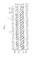
- FIG. 1 is a plan view illustrating a layout of a TFT substrate included in a conventional semi-transmissive liquid crystal display device disclosed in Japanese Patent Application Laid-open No. 2000-111902 and FIG. 2 is a cross sectional view of a liquid crystal panel employed in the conventional semi-transmissive liquid crystal display device, taken along the line A-A of FIG. 1 .
- a red color pixel 101R, a green color pixel 101G and a blue color pixel 101B are disposed in this order in a direction in which a scanning signal line extends.
- a thin film transistor (TFT) 102 is formed in each pixel.
- the thin film transistor 102 consists of a gate electrode 103a projecting from a gate line 103 as the scanning signal line and a drain electrode 104a projecting from a drain line 104 that extends in a direction perpendicular to the gate line.
- the gate line 103 and the gate electrode 103a are formed on a transparent substrate 100a and further, an insulation film 105 is formed on the transparent substrate 100a covering the gate line 103 and the gate electrode 103a.
- the drain line 104 is formed on the insulation film 105.
- An amorphous silicon layer 106 is formed on the insulation film 105 to face the gate electrode 103a and the drain electrode 104a is formed extending on the amorphous silicon layer 106.
- a source electrode 107 is formed extending from the amorphous silicon layer 106 in a direction apart from the drain electrode 104a while a part of the source electrode is at least positioned on and inside the amorphous silicon layer.
- a reflective display section of each pixel projecting portions 108 are formed on the insulation film 105 and within a transmissive display section, a transparent electrode 109 is formed on the insulation film 105.
- the reflective display section is formed to surround the transmissive display section.
- an insulation film 110 covering the projecting portions 108, the thin film transistor 102 and the like is formed and further, a contact hole 111 is formed in the insulation film 110 so as to reach the surface of the source electrode 107.
- a reflective electrode 112 is formed within the contact hole 111 and on the insulation film 105.
- the reflective electrode 112 has a convex-concave surface reflecting the profile of the projecting portions 108.
- the reflective electrode 112 is connected also to the transparent electrode 109. Furthermore, a retardation film 113 and a polarizer 114 are formed on the transparent substrate 100a on a side thereof defined as the surface on which elements such as the thin film transistor 102 are not formed.
- the elements constructed as described above constitute a TFT substrate.
- another transparent substrate 100b is disposed in parallel with the transparent substrate 100a on a side thereof defined as the surface on which the thin film transistor 102 is formed.
- a color filter (CF) 121 and an opposing electrode 122 are formed on a surface of the transparent substrate 100b on a side thereof facing the transparent substrate 100a.
- the color filter 121 is formed extending in parallel with the drain line 104 and further, when viewing a pixel in a direction perpendicular to a surface of the associated transparent substrate, the transparent electrode 109 is being formed inside with respect to both end lines of the color filter 121 whereas the reflective electrode 112 is being formed to have a width extending beyond the both lines thereof.
- a retardation film 123 and a polarizer 124 are formed on the transparent substrate 100b on a side thereof defined as the surface on which elements such as the color filter 121 are not formed.
- the elements constructed as described above constitute a CF substrate.
- liquid crystal 130 is interposed between the TFT substrate and the CF substrate to constitute the liquid crystal panel.
- the conventional color liquid crystal display device constructed as described above has one kind of color filter therein corresponding to each color and therefore, can be manufactured through a reduced number of process steps, thereby improving a yield thereof.
- the color liquid crystal display device can offer a display brightness greater than that could be achieved in a color liquid crystal display device developed before the emergence of color liquid crystal display device employing such construction of the color filter 121.
- the conventional reflective liquid crystal display device has projecting portions formed under the reflective electrode and extending in all directions.
- the projecting portions are designed to have a pattern optimal in terms of paths of an incident light and a reflected light.
- FIG. 3 illustrates a layout of projecting portions employed in the conventional liquid crystal display device.
- the projecting portions 108 are formed without especially taking into account the effect of boundaries between pixels.
- a liquid crystal display device having a transmissive display section and a reflective display section therein includes such projecting portions only within the reflective display section.
- the conventional semi-transmissive liquid crystal display device employing one kind of color filter corresponding to each pixel in order to, for example, reduce the number of process steps to be carried out to manufacture the device has an image quality inferior to that of a device employing two kinds of color filters therein, which has been developed before the emergence of the device employing one kind of color filter.
- An object of the present invention is to provide a color liquid crystal panel capable of improving quality of images to be displayed in a semi-transmissive liquid crystal display device, a method for manufacturing the same, and further a color liquid crystal display device employing the same.
- a color liquid crystal panel comprises a thin film transistor, a reflective electrode connected to the thin film transistor and a transparent electrode in each pixel thereof. Furthermore, the color liquid crystal panel is constructed such that a display surface of the color liquid crystal panel allows a light emitted from a backlight to exit from the display surface through the transparent electrode and another light inputted to the display surface to exit from the display surface after being reflected by the reflective electrode.
- the color liquid crystal panel is constructed such that the color liquid crystal panel has a color filter therein so that at least one opening varying an area thereof depending on a color to be displayed is formed in the color filter in a part thereof facing the reflective electrode, and color reproduction ranges of the light exiting from the display surface through the transparent electrode and the another light exiting from the display surface after being reflected by the reflective electrode substantially coincide with each other.
- the color liquid crystal panel of the first aspect of the present invention is further and preferably constructed as follows. That is, a red color filter, a green color filter and a blue color filter are respectively formed as the color filter and a ratio of an area of the at least one opening formed in the color filter with respect to an area of the color filter becomes maximum in the event the green color filter is selected as the color filter to calculate the ratio.
- the color liquid crystal panel is more preferably constructed as follows.
- the ratio of an area of the at least one opening formed in the green color filter with respect to an area of the green color filter is made two to four times the ratio of an area of the at least one opening formed in one of the red color filter and the blue color filter with respect to an area of associated one of the red color filter and the blue color filter.
- the color liquid crystal panel of the first aspect of the present invention described so far is preferably constructed as follows. That is, the ratio of an area of the at least one opening formed in the color filter with respect to an area of the color filter in the color filter in a part thereof facing the reflective electrode is set at a value of not greater than 50% and further, the at least one opening is formed shaped like a slit and a width of the slit is set at a value of 1 ⁇ m to 10 ⁇ m.
- a color liquid crystal panel constructed in accordance with the second aspect of the present invention has a thin film transistor, a reflective electrode connected to the thin film transistor and a transparent electrode in each pixel thereof. Furthermore, the color liquid crystal panel is constructed such that a display surface of the color liquid crystal panel allows a light emitted from a backlight to exit from the display surface through the transparent electrode and another light inputted to the display surface to exit from the display surface after being reflected by the reflective electrode.
- the color liquid crystal panel comprises a color filter and a transparent film formed between the color filter and a transparent substrate while varying a volume thereof depending on a color to be displayed, in which color reproduction ranges of the light exiting from the display surface through the transparent electrode and the another light exiting from the display surface after being reflected by the reflective electrode substantially coincide with each other.
- a color liquid crystal panel constructed in accordance with the third aspect of the present invention comprises a transparent substrate, a thin film transistor formed in each pixel on the transparent substrate, an insulation film formed on the transparent substrate to have a convex-concave surface within the each pixel, a reflective electrode formed on the insulation film and connected to the thin film transistor in the each pixel, in which the insulation film has projecting portions each extending along a boundary between adjacent pixels and having a width substantially equal to that of projecting portions constituting the convex-concave surface within the each pixel.
- the present invention has been conceived to have the following construction of liquid crystal panel. That is, as described above, an area of openings formed in a color filter within a reflective display section is made to vary depending on a color to be displayed or a transparent film is formed between a color filter and a transparent substrate while varying the volume of the transparent film depending on a color to be displayed.
- liquid crystal panel makes the color reproduction ranges of a transmissive display section and a reflective display section coincide with each other corresponding to a color to be displayed, in other words, with respect to individual colors to be displayed, thereby creating color balanced viewable images corresponding to a color to be displayed, in other words, with respect to individual colors to be displayed, and further achieving high quality images.
- the inventors found that images appearing pale yellow in color are caused by the difference in gaps between two substrates at positions thereof located within a pixel and between pixels. Normally in a reflective liquid crystal display device, a black matrix is not formed at the boundary between pixels to make a display bright. For this reason, it is believed that the above-described difference in gaps makes a light travel different distances through a liquid crystal to generate phase difference of light, making images appear pale yellow in color. Therefore, the liquid crystal panel of the present invention is constructed such that projecting portions are formed also at the boundary between pixels to reduce the difference in gaps to thereby reduce pale yellow in color and achieve high quality images.
- a method for manufacturing a color liquid crystal panel according to the present invention is constructed as follows. First, the color liquid crystal panel has a thin film transistor, a reflective electrode connected to the thin film transistor and a transparent electrode in each pixel thereof, and is further constructed such that a display surface of the color liquid crystal panel allows a light emitted from a backlight to exit from the display surface through the transparent electrode and another light inputted to the display surface to exit from the display surface after being reflected by the reflective electrode.
- the method for manufacturing the above-described color liquid crystal panel comprises the steps of: preparing a photomask in such a manner that at least one opening is formed in the photomask so as to vary an area of the at least one opening depending on a color to be displayed; and forming the pattern in a raw material film constituting the color filter by using the photomask to make the color filter have the at least one opening therein varying depending on a color to be displayed and facing the reflective electrode.
- the method for manufacturing a color liquid crystal panel prefferably has a step of forming a transparent film covering all color filters formed corresponding to colors to be displayed and a step of flattening the transparent film after a step of forming the color filter.
- the color liquid crystal panel constructed in accordance with the first aspect of the present invention and capable of displaying high quality images can be fabricated.
- a color liquid crystal display device of the present invention comprises a liquid crystal panel constructed in accordance with one of the first, second and third aspects of the present invention.
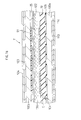
- FIG. 4 is a plan view of a layout of a TFT substrate employed in a liquid crystal panel constructed in accordance with the first embodiment of the present invention.
- FIG. 5 is a cross sectional view taken along the line A-A of FIG.4
- FIG. 6 is a cross sectional view taken along the line B-B of FIG.4
- FIG. 7 is a cross sectional view taken along the line C-C of FIG.4 .
- the first embodiment also employs the following construction of liquid crystal panel similar to that described in the conventional liquid crystal display device. That is, the liquid crystal panel of the first embodiment is constructed such that a red color pixel 101R, a green color pixel 101G and a blue color pixel 101B are disposed in this order in a direction in which a scanning signal line extends.
- a thin film transistor (TFT) 102 is formed in each pixel.
- the thin film transistor 102 consists of a gate electrode 103a projecting from a gate line 103 as the scanning signal line and a drain electrode 104a projecting from a drain line 104 that extends in a direction perpendicular to the gate line.
- the gate line 103 and the gate electrode 103a are formed on a transparent substrate 100a and further, an insulation film 105 is formed on the transparent substrate 100a covering the gate line 103 and the gate electrode 103a.
- the drain line 104 is formed on the insulation film 105.
- An amorphous silicon layer 106 is formed on the insulation film 105 to face the gate electrode 103a and the drain electrode 104a is formed extending on the amorphous silicon layer 106.
- a source electrode 107 is formed extending from the amorphous silicon layer 106 in a direction apart from the drain electrode 104a while a part of the source electrode is at least positioned on and inside the amorphous silicon layer.
- each pixel is partitioned into, for instance, nearly two equal sections, i.e., a reflective display section R and a transmissive display section T, by a line extending in parallel with the scanning signal line.
- the reflective display section R is disposed in a pixel in a section thereof including the thin film transistor 102.
- projecting portions 8 are formed on the insulation film 105.
- the projecting portions 8 consist of, for example, an insulation film.
- an insulation film 10 is formed covering the projecting portions 8, the thin film transistor 102 and the like and further, a contact hole 11 is formed in the insulation film 10 so as to reach the surface of the source electrode 107.
- a reflective electrode 12 is formed within the contact hole 11 and on the insulation film 10. The reflective electrode 12 has a convex-concave surface reflecting the profile of the projecting portions 8.
- a transparent electrode 9 is formed on the insulation film 10 and the reflective electrode 12 and the transparent electrode 9 overlap each other around the boundary between the reflective display section R and the transmissive display section T.
- a retardation film 113 and a polarizer 114 are formed on the transparent substrate 100a on a side thereof defined as the surface on which elements such as the thin film transistor 102 are not formed.
- the elements constructed as described above constitute a TFT substrate.
- another transparent substrate 100b is disposed in parallel with the transparent substrate 100a on a side thereof defined as the surface on which the thin film transistor 102 is formed.
- a color filter (CF) 21 is formed on a surface of the transparent substrate 100b on a side thereof facing the transparent substrate 100a. As shown in FIGS. 4 through 7 , the color filter 21 is formed extending in parallel with the drain line 104 and further, when viewing a pixel in a direction perpendicular to a surface of the associated transparent substrate, the transparent electrode 9 and the reflective electrode 12 are formed inside with respect to both end lines of the color filter 21. In addition, within the reflective display section R, slits 21a are formed in the color filter 21.
- the slits 21a are formed to have a width of, for instance, 1 ⁇ m to 10 ⁇ m and further, to occupy, for instance, below 50% of an area of the color filter 21 within the reflective display section R.
- the ratio of an area occupied by the slits 21a with respect to an area of the color filter 21 within the reflective display section R varies depending on a color to be displayed and in the embodiment, the ratio of an area occupied by the slits 21a that are formed in the green color pixel 101G is made, for example, three times the respective ratio of an area occupied by the slits 21a that are formed in the red color pixel 101R and the blue color pixel 101B.
- the embodiment is constructed such that the slits 21a are formed extending in a direction in parallel with the color filter 21, the embodiment is not limited to the above-described construction of slits and therefore, may be constructed by employing another slits that have patterns different from that of the slits 21a.
- an overcoat layer 25 is formed on the transparent substrate 100b filling the slits 21a while covering the color filter 21 and an opposing electrode 122 is formed on the overcoat layer 25.
- the overcoat layer 25 consists of, for example, a transparent resin and the opposing electrode 122 consists of, for example, an ITO (Indium Tin Oxide).
- a retardation film 123 and a polarizer 124 are formed on a surface of the transparent substrate 100b on a side thereof defined as the surface on which elements such as the color filter 21 are not formed.
- the elements constructed as described above constitute a CF substrate.
- a liquid crystal 130 is interposed between the TFT substrate and the CF substrate.
- a light emitted from a backlight exits to the outside through the color filter 21.
- a part of a light reaching the reflective electrode 12 through the color filter 21 exits to the outside through the slits 21a and a part of a light reaching the reflective electrode 12 through the slits 21a exits to the outside through the color filter 21.
- the following phenomenon can be seen in the reflective display section R. That is, a light reaching the reflective electrode 12 through the color filter 21 exits to the outside through the color filter 21 and a light reaching the reflective electrode 12 through the slits 21a exits to the outside through the slits 21a.
- a mean film thickness of a color filter through which lights exiting from the reflective display section R transmit during the time in which the lights travel the associated distance after they are inputted to the inside until they are outputted to the outside becomes nearly equal to that could be observed in the transmissive region T.
- the ratio is referred to as "aperture ratio"
- the color liquid crystal display panel constructed as described above can display high quality images.
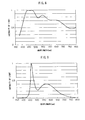
- the inventors of this application carried out a simulation in the following manner to make the above-described relationship clearer: first, decide to use a white-colored light emitting diode (LED) as a backlight; secondly, vary the film thickness of color filter; thirdly, with respect to various film thicknesses of color filter, calculate the aperture ratio so as to take the value for allowing chromaticity coordinates of the transmissive display section to substantially match to the CIE (Center for International Education) chromaticity coordinates of a white display.
- a standard light CIE "C” was used as a light incident on the reflective display section.
- FIG. 8 is a graphic illustration of a spectrum of the standard light CIE "C" and FIG.
- FIG. 9 is a graphic illustration of a spectrum of a light emitted from a white-colored LED. Note that an intensity of light along the longitudinal axis shown in FIGS. 8 and 9 is normalized such that the maximum intensity of light takes the value of one. The results obtained by carrying out the above-mentioned simulation will be illustrated in the following Tables 1 through 7.
- Table 1 Film thickness 0.8 ⁇ m Hue Aperture ratio x coordinate value y coordinate value NTSC ratio Transmissive display section Red - 0.417 0.328 Green - 0.329 0.377 Blue - 0.229 0.288 White - 0.321 0.366 0.040 Reflective display section (having optimal slits) Red 0.20 0.417 0.319 Green 0.38 0.319 0.378 Blue 0.27 0.239 0.288 White - 0.318 0.334 0.042 Reflective display section (having no slits) Red 0 0.487 0.306 Green 0 0.316 0.417 Blue 0 0.171 0.247 White - 0.311 0.336 0.142 Table 2 Film thickness 1.0 ⁇ m Hue Aperture ratio x coordinate value y coordinate value NTSC ratio Transmissive display section Red - 0.430 0.328 - Green - 0.328 0.385 - Blue - 0.217 0.279 - White - 0.321 0.337 0.054 Reflective display section (hav
- the NTSC ratio is a ratio of an area of a color reproduction range of the associated display section with respect to an area of a color reproduction range most suitable for television display and defined by NTSC (National Television System Committee).
- FIG. 10 is a CIE chromaticity diagram showing a color reproduction range most suitable for television display and defined by NTSC.
- the chromaticity coordinates and NTSC ratio calculated with respect to the transmissive display section substantially match to those calculated with respect to the reflective display section.
- the chromaticity coordinates and NTSC ratio calculated with respect to the transmissive display section are extensively different from those calculated with respect to the reflective display section.
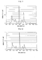
- FIG. 11 is a graphic illustration of a spectrum of the light emitted from the first three-wavelength light source. Note that an intensity of light along the longitudinal axis shown in FIG.
- Table 8 Film thickness 1.2 ⁇ m Hue Aperture ratio x coordinate value y coordinate value NTSC ratio Transmissive display section Red - 0.447 0.291 - Green - 0.335 0.387 - Blue - 0.216 0.252 - White - 0.329 0.317 0.084 Reflective display section (having optimal slits) Red 0.15 0.448 0.321 - Green 0.40 0.317 0.387 - Blue 0.10 0.191 0.252 - White - 0.313 0.331 0.082
- Table 9 Film thickness 1.6 ⁇ m Hue Aperture ratio x coordinate value y coordinate value NTSC ratio Transmissive display section Red - 0.476 0.292 - Green - 0.333 0.407 - Blue - 0.197 0.234 - White - 0.330 0.320 0.128 Reflective display section
- the film thickness of a color filter is fixed to be 1.6 ⁇ m and the aforementioned white-colored LED, the first three-wavelength light source and an additional three-wavelength light source (the second three-wavelength light source) are employed as a light source.
- FIG. 12 is a graphic illustration of a spectrum of a light emitted from the second three-wavelength light source. Note that an intensity of light along the longitudinal axis shown in FIG. 12 is normalized such that the maximum intensity of light takes the value of one.
- Tables 11 through 13 The results obtained by carrying out the above-mentioned simulation will be illustrated in the following Tables 11 through 13 in which the white-colored LED, the first three-wavelength light source and the second three-wavelength light source are employed, respectively.
- the results obtained by those simulations tell that regardless of a light source to be employed in the simulation, it is desirable to make the aperture ratio applied to the green color filter largest among three aperture ratios applied to the red, green and blue color filters. Specifically, in the case where a white-colored light source is employed in the simulation, it is preferable that the aperture ratio applied to the green color filter is made two to four times those applied to the red and blue color filters.
- the slits of the color filter are formed to have a width of 1 ⁇ m to 10 ⁇ m.
- the slits are formed to have a width narrower than 1 ⁇ m, operation for forming associated patterns in the color filter becomes difficult.
- the slits are formed to have a width wider than 10 ⁇ m, operation for flattening an overcoat layer formed on the color filter becomes difficult.
- FIGS. 13A, 13B and 13C are plan views illustrating patterns of various color filters and positional relationship between reflective display and transmissive display sections within a pixel.
- the liquid crystal panel of the present invention may employ an opening 41a that is formed in the color filter 41 so as to be positioned in the center of the reflective display section R.
- the liquid crystal panel of the present invention may employ an opening 42a that is formed in a color filter 42 so as to be positioned in the center of the reflective display section R.
- the liquid crystal panel of the present invention may employ the following construction of pixel. That is, the pixel is constructed such that a color filter 43 is formed to have its end lines 43a positioned nearer the transmissive display section T than the outer end lines of the two reflective display sections R, thereby creating regions in the pixel in which the color filter 43 is not formed.
- the ratio of an area of openings with respect to that of the reflective display section is made equal to or less than 50%.
- the reason is as follows. That is, when the color filter is formed to occupy less than 50% of an entire area of the reflective display section, the ratio of lights that have no opportunities to transmit through the color filter during the time in which the lights travel the associated distance after they are inputted to the inside until they are outputted to the outside with respect to entire lights associated with the reflective display section increases, thereby making it difficult for the color reproduction range of the reflective display section to coincide with that of the transmissive display section.
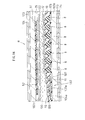
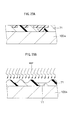
- FIGS. 14 , 15 and 16 are cross sectional views, each illustrating a structure of a liquid crystal panel of the second embodiment constructed in accordance with the present invention, taken along the line A-A of FIG.4 , the line B-B of FIG.4 and the line C-C of FIG.4 , respectively.
- the parts and components used in the second embodiment shown in FIGS. 14 , 15 , 16 and also used in the first embodiment shown in FIGS. 4 , 5 , 6 , 7 , 8 are denoted by the same numerals as those referred in the first embodiment, thereby omitting detailed explanation thereof.
- the second embodiment also includes the following construction of liquid crystal panel similar to that described in the first embodiment. That is, the liquid crystal panel of the second embodiment is constructed such that each pixel is partitioned into, for example, nearly two equal sections, i.e., a reflective display section R and a transmissive display section T, by a line extending in parallel with the scanning signal line. Furthermore, a TFT substrate is constructed in the same manner as that employed in the first embodiment.
- a CF substrate of the second embodiment is constructed such that a color filter 51 is formed on a surface of a transparent substrate 100b on a side thereof facing a transparent substrate 100a.
- a transparent resin layer 52 is formed between the color filter 51 and the transparent substrate 100b.
- the ratio of a volume of the transparent resin layer 52 with respect to an entire volume of the color filter 51 and the transparent resin layer 52 within the reflective display section R (hereinafter, the ratio is referred to as "volume ratio") is set at a value of, for example, 35% to 65%.
- the volume ratio can be adjusted by varying a film thickness or an area of the transparent resin layer 52.
- the volume ratio varies depending on a color to be displayed and in the embodiment, the volume ratio applied to a green color pixel 101G is made, for example, about three times the volume ratio applied to a red color pixel 101R and a blue color pixel 101B.
- the embodiment is constructed such that the transparent resin layer 52 is formed completely overlapping the color filter 51, the embodiment is not limited to the above-described construction of transparent resin layer and color filter. Additionally, it would be desirable that the color filter 51 has a flat surface in the same plane over two areas thereof corresponding to the reflective display section R and the transmissive display section T.
- a light emitted from a backlight exits to the outside through the color filter 51.
- a light reaching the reflective electrode 12 through the color filter 51 exits to the outside through the color filter 51.
- the substantial film thickness of color filter through which lights transmit during the time in which the lights travel the associated distance after they are inputted to the inside until they are outputted to the outside becomes nearly equal to that could be observed within the transmissive display section T.
- the volume ratio calculated with respect to the volume of the transparent resin layer 52 is made to vary depending on a color to be displayed, it becomes possible for the color reproduction range of the reflective display section R to coincide with that of the transmissive display section T, thereby allowing the liquid crystal panel to display high quality images.
- Table 14 Film thickness 2.2 ⁇ m Hue Area ratio Volume ratio x coordinate value y coordinate value NTSC ratio Transmissive display section Red - - 0.518 0.333 Green - - 0.325 0.43 Blue - - 0.161 0.227 White - - 0.319 0.342 0.175 Reflective display section (having optimal transparent resin layer) Red 0.82 0.58 0.51 0.309 Green 0.98 0.41 0.314 0.427 Blue 0.70 0.48 0.158 0.23 White - - 0.313 0.34 0.18
- Table 15 Film thickness 2.0 ⁇ m Hue Area ratio Volume ratio x coordinate value y coordinate value NTSC ratio Transmissive display section Red - - 0.506 0.331 Green - - 0.325 0.423 Blue - - 0.167 0.234 White - - 0.319 0.341 0.154 Reflective display section (having optimal transparent resin layer) Red 0.80 0.60 0.501 0.308 Green 1.00
- area ratio indicated in the tables represents the ratio of an area of transparent resin layer with respect to an area of color filter within the reflective display section and "volume ratio” represents the ratio of a volume of transparent resin layer with respect to an entire volume of color filter and transparent resin layer within the reflective display section.
- film thickness represents a film thickness of color filter within the transmissive display section, coinciding with an entire film thickness of color filter and transparent resin layer within the reflective display section.
- the chromaticity coordinates and NTSC ratio calculated with respect to the transmissive display section substantially match to those calculated with respect to the reflective display section.
- a method for manufacturing the liquid crystal panel of the first embodiment will be explained below.
- a TFT substrate can be manufactured by using the same method as that employed to manufacture the conventional liquid crystal panel.
- a CF substrate can be manufactured using, for instance, the following method: first, coat a photosensitive resin film as a raw material film that constitutes a monochrome color filter on a transparent substrate 100b; secondly, expose the photosensitive resin film using a photomask that has a predetermined slit pattern therein and then, develop the photosensitive resin film. Through those steps, the photosensitive resin film is patterned to constitute a monochrome color filter 21 having slits 21a therein. Those steps are carried out to form three color filters 21 respectively.
- the ratio of an area of a pattern to be formed in the photomask corresponding to the slits with respect to an area of the photomask is made maximum when using a photomask to form a green color filter. That is, the ratios applied to the associated color filters are individually adjusted.
- the photomasks are individually formed to have a pattern associated with a slit pattern formed in the color filter and corresponding to a color to be displayed.
- the ratio of an area of slit pattern with respect to an area of the photomask used to form a green color filter is made about two to four times that should be applied to a photomask to form a red or blue color filter.
- an overcoat layer is formed on an entire surface of the transparent substrate 100b while achieving flatness thereof and further, an opposing electrode is formed thereon. Furthermore, a retardation film and a polarizer are formed on a surface of the transparent substrate 100b on a side thereof defined as the surface on which the color filter is not formed.
- a method for manufacturing the liquid crystal panel of the second embodiment will be explained below.
- a TFT substrate can be manufactured by using the same method as that employed to manufacture the conventional liquid crystal panel.
- a CF substrate can be manufactured using, for instance, the following method: first, previously prepare photomasks in such a manner that the photomasks each are formed corresponding to a color to be displayed to have a pattern therein corresponding to a pattern of transparent resin film; secondly, coat a raw material film that constitutes a transparent resin film on a transparent substrate 100b; thirdly, form an associated pattern in the raw material film using the above-described photomask followed by formation of a transparent resin film 52 on the transparent substrate 100b; fourthly, coat another raw material film that constitutes a color filter on the transparent substrate 100b and then, carry out associated process steps of, for instance, exposing and developing the another raw material film to form the color filter so as to have a flat surface thereof corresponding to a color to be displayed.
- the ratio of an area of a pattern formed in the photomask and corresponding to a pattern of transparent resin film with respect to an area of photomask is made maximum when using the photomask to form a green color filter. That is, the ratios applied to the associated color filters are individually adjusted. In other words, the photomasks are individually formed to have a pattern corresponding to a pattern of transparent resin film and a color to be displayed.
- the ratio of an area of a pattern formed in the photomask with respect to an area of photomask, which is applied to a photomask used to form a green color filter is made about two to four times that should be applied to a photomask to form a red or blue color filter.
- an overcoat layer is formed on an entire surface of the transparent substrate 100b while achieving flatness thereof and further, an opposing electrode is formed thereon. Furthermore, a retardation film and a polarizer are formed on the transparent substrate 100b on a backside thereof defined as the surface on which the color filter is not formed.
- the liquid crystal panel employed in the first and second embodiments does not have a black matrix between the adjacent color filters of the CF substrate, the liquid crystal panel may be constructed such that the black matrix is formed between the adjacent color filters of the CF substrate.
- the liquid crystal panel employed in the first and second embodiments have a color filter formed on a transparent substrate on which a thin film transistor is not formed, the liquid crystal panel may be constructed such that the color filter is formed on a substrate on which a thin film transistor is formed. In this case, the color filter is formed on, for example, a reflective electrode or a transparent electrode.
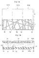
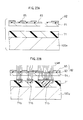
- FIG. 17A is a layout diagram indicating projecting portions formed under a reflective electrode in the liquid crystal panel of the third embodiment of the present invention and FIG. 17B is a schematic cross sectional view of the liquid crystal panel.
- the projecting portions 8 are formed under the reflective electrode in all directions to make the reflective electrode have a convex-concave surface that reflects the profile of the projecting portions.
- projecting portions 58 formed in the same step through which the projecting portions 8 are formed are formed in boundary regions between pixels that are located adjacent to each other in a direction in which a scanning signal line (gate line) extends.
- the width and height of the projecting portion 58 are substantially the same as those of the projecting portion 8.
- difference between a gap "d1" between a color filter 21 and an insulation film 10 under the reflective electrode within a pixel and a gap "d2" between a transparent substrate 100b and the insulation film 10 in the boundary regions between pixels is made to become shorter than that observed in the conventional liquid crystal panel.
- a gap between the undesirable boundary regions and the transparent substrate 100b becomes extremely long in comparison with the gap observed in the embodiment in which such undesirable boundary regions never exist.
- images appearing pale yellow in color are substantially eliminated from a display thereof.
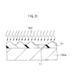
- FIG. 18 is a schematic diagram to explain the relationship between a width of projecting portion and a height thereof that varies depending on the width.
- the projecting portions 8 are omitted whereas the projecting portions 58 are drawn.
- the liquid crystal panel shown in FIG. 14 and FIG. 16 is also constructed as described above, that is, constructed such that the projecting portions 58 having the same width and height as those of the projecting portions 8 are being formed in addition to the projecting portions 8.
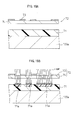
- FIGS. 19A, 19B , 20A, 20B and 21 are schematic diagrams showing the method for manufacturing the projecting portions through two exposure steps in order.
- the depth of exposure is preferably limited to the position located, for example, about half the film thickness of the resist film 71 consisting of a photosensitive resin down from the surface of the resist film.
- a photomask 75 in such a manner that a Cr film 76 having an opening only in a part thereof corresponding to a contact hole 11 is formed on a transparent substrate 74. Then, expose the resist film 71 consisting of a photosensitive resin using the photomask 75 to form another exposed portion 71a in the resist film 71, which corresponds to the portion of the resist film where the contact hole 11 will be formed later on, so as to reach the surface of a source electrode (not shown).
- FIGS. 22A, 22B , 23A and 23B are schematic diagrams showing the method for manufacturing the projecting portions through one exposure step in order.
- a photomask 82 in the following manner. That is, a semi-transparent film 83 having an opening only in a part thereof corresponding to a contact hole 11 is formed on a transparent substrate 84 and further, a Cr film 85 that prevents a light from being incident on the resist film 71 on a part thereof corresponding to the projecting portions is formed on the semi-transparent film.
- the semi-transparent film 83 consists of, for instance, a metal oxide film.
- the depth of exposure through the semi-transparent film 83 is preferably limited to the position located, for example, about half the film thickness of the resist film 71 consisting of a photosensitive resin down from the surface of the resist film.
- the exposed portion 71b is formed in the resist film 71 consisting of a photosensitive resin.
- a portion, corresponding to the contact hole 11, out of the exposed portion 71b, directly receives an exposure light that does not transmit through the semi-transparent film 83 and therefore, the depth of exposure is positioned in proximity to the surface of a source electrode (not shown).
- the embodiment employs a resist film consisting of a photosensitive resin to form projecting portions
- the embodiment may employ the following method for manufacturing projecting portions. That is, for example, form a plurality of projecting portions consisting of an insulation film and further, form another insulation film thereon covering an entire surface of the insulation film, thereby forming a convex-concave surface within pixels and in a boundary between pixels.
- liquid crystal panel of the present invention may be constructed by combining one of the constructions of liquid crystal panel employed in the first and second embodiments with the construction of liquid crystal panel employed in the third embodiment.
- FIG. 24 is a block diagram illustrating the configuration of a portable information terminal constructed in accordance with the embodiment of the present invention.
- FIG. 25 is a block diagram illustrating the configuration of a portable telephone constructed in accordance with an embodiment of the present invention.
- a portable information terminal 250 constructed in accordance with the embodiment of the present invention includes a display unit 268 comprised of a liquid crystal panel 265, a backlight unit 266 and an image signal processing unit 267 for processing an image signal. Furthermore, the portable information terminal 250 includes a control unit 269 for controlling components that constitute the portable information terminal 250, a storage unit 271 for storing programs executed by the control unit 269 and various data, a communication unit 272 for transmitting data to and receiving data from external devices, an input unit 273 comprised such as of a keyboard or a pointer and a power supply unit 274 for supplying power to the components that constitute the portable information terminal 250. Note that the first, second and third embodiments described above are applied to the liquid crystal panel 265.
- the portable information terminal 250 thus constructed in accordance with the embodiment is able to display high quality images by creating color balanced viewable images or suppressing pale yellow in color.
- a portable telephone 275 constructed in accordance with the embodiment of the present invention includes a display unit 276 comprised of a liquid crystal panel 265, a backlight unit 266 and an image signal processing unit 267 for processing an image signal. Furthermore, the portable telephone 275 includes a control unit 277 for controlling components that constitute the portable telephone 275, a storage unit 278 for storing programs executed by the control unit 277 and various data, a transmission unit 281 for transmitting a radio signal to external devices, an input unit 282 comprised such as of a keyboard or a pointer and a power supply unit 283 for supplying power to the components that constitute the portable telephone 275. Note that the first, second and third embodiments described above are applied to the liquid crystal panel 265.
- the portable telephone 275 thus constructed in accordance with the embodiments also is able to display high quality images by creating color balanced viewable images or suppressing pale yellow in color.
- a color liquid crystal panel having advantageous constructions of color liquid crystal panel described so far can be applied to a color liquid crystal display device.
Applications Claiming Priority (2)
| Application Number | Priority Date | Filing Date | Title |
|---|---|---|---|
| JP2001117041A JP4583650B2 (ja) | 2001-04-16 | 2001-04-16 | カラー液晶パネル、その製造方法及びカラー液晶表示装置 |
| EP02008507A EP1251389A3 (fr) | 2001-04-16 | 2002-04-15 | Panneau d'affichage en couleurs à cristal liquide et procédé pour sa fabrication |
Related Parent Applications (1)
| Application Number | Title | Priority Date | Filing Date |
|---|---|---|---|
| EP02008507A Division EP1251389A3 (fr) | 2001-04-16 | 2002-04-15 | Panneau d'affichage en couleurs à cristal liquide et procédé pour sa fabrication |
Publications (2)
| Publication Number | Publication Date |
|---|---|
| EP2793074A2 true EP2793074A2 (fr) | 2014-10-22 |
| EP2793074A3 EP2793074A3 (fr) | 2015-04-08 |
Family
ID=18967670
Family Applications (3)
| Application Number | Title | Priority Date | Filing Date |
|---|---|---|---|
| EP11151241.4A Withdrawn EP2348352A3 (fr) | 2001-04-16 | 2002-04-15 | Écran couleur à cristaux liquides, ses procédés de fabrication et dispositif à écran couleur à cristaux liquides l'utilisant |
| EP20140002491 Withdrawn EP2793074A3 (fr) | 2001-04-16 | 2002-04-15 | Écran couleur à cristaux liquides, son procédé de fabrication et dispositif d'affichage couleur à cristaux liquides l'utilisant |
| EP02008507A Withdrawn EP1251389A3 (fr) | 2001-04-16 | 2002-04-15 | Panneau d'affichage en couleurs à cristal liquide et procédé pour sa fabrication |
Family Applications Before (1)
| Application Number | Title | Priority Date | Filing Date |
|---|---|---|---|
| EP11151241.4A Withdrawn EP2348352A3 (fr) | 2001-04-16 | 2002-04-15 | Écran couleur à cristaux liquides, ses procédés de fabrication et dispositif à écran couleur à cristaux liquides l'utilisant |
Family Applications After (1)
| Application Number | Title | Priority Date | Filing Date |
|---|---|---|---|
| EP02008507A Withdrawn EP1251389A3 (fr) | 2001-04-16 | 2002-04-15 | Panneau d'affichage en couleurs à cristal liquide et procédé pour sa fabrication |
Country Status (6)
| Country | Link |
|---|---|
| US (5) | US6897922B2 (fr) |
| EP (3) | EP2348352A3 (fr) |
| JP (1) | JP4583650B2 (fr) |
| KR (1) | KR100468440B1 (fr) |
| NO (2) | NO336130B1 (fr) |
| TW (1) | TW591297B (fr) |
Families Citing this family (30)
| Publication number | Priority date | Publication date | Assignee | Title |
|---|---|---|---|---|
| JP3941481B2 (ja) * | 2000-12-22 | 2007-07-04 | セイコーエプソン株式会社 | 液晶表示装置および電子機器 |
| JP3642051B2 (ja) * | 2002-01-23 | 2005-04-27 | ソニー株式会社 | 液晶表示装置 |
| WO2003085450A1 (fr) * | 2002-04-04 | 2003-10-16 | Sony Corporation | Ecran a cristaux liquides |
| JP2004145275A (ja) * | 2002-08-27 | 2004-05-20 | Seiko Epson Corp | 着色層材料、カラーフィルタ基板、電気光学装置及び電子機器、カラーフィルタ基板の製造方法、並びに電気光学装置の製造方法 |
| US7248315B2 (en) * | 2002-08-30 | 2007-07-24 | Casio Computer Co., Ltd. | Liquid crystal display device capable of transmission display and reflection display |
| JP4489346B2 (ja) * | 2002-12-17 | 2010-06-23 | シャープ株式会社 | 液晶表示装置 |
| JP4233862B2 (ja) * | 2002-12-17 | 2009-03-04 | ティーピーオー ホンコン ホールディング リミテッド | カラーフィルタ及びこれを用いた液晶表示装置並びにその製造方法 |
| KR100491258B1 (ko) * | 2002-12-31 | 2005-05-24 | 엘지.필립스 엘시디 주식회사 | 반사투과형 액정표시장치용 어레이기판과 그 제조방법 |
| US7379651B2 (en) * | 2003-06-10 | 2008-05-27 | Abu-Ageel Nayef M | Method and apparatus for reducing laser speckle |
| CN100397180C (zh) * | 2003-11-17 | 2008-06-25 | 鸿富锦精密工业(深圳)有限公司 | 液晶显示器 |
| JP4123183B2 (ja) * | 2004-04-20 | 2008-07-23 | ソニー株式会社 | 定電流駆動装置、バックライト光源装置及びカラー液晶表示装置 |
| JP4647936B2 (ja) * | 2004-05-31 | 2011-03-09 | 株式会社 日立ディスプレイズ | 液晶表示装置 |
| KR20060018137A (ko) * | 2004-08-23 | 2006-02-28 | 삼성전자주식회사 | 반투과 액정표시장치와 그 제조방법 |
| JP4427436B2 (ja) * | 2004-11-25 | 2010-03-10 | シャープ株式会社 | 液晶表示装置 |
| KR101125248B1 (ko) * | 2004-12-23 | 2012-03-21 | 엘지디스플레이 주식회사 | 반투과형 컬러필터 기판 및 그 제조방법 |
| JP4305437B2 (ja) * | 2005-05-19 | 2009-07-29 | エプソンイメージングデバイス株式会社 | 電気光学装置及び電子機器 |
| JP4211773B2 (ja) * | 2005-05-19 | 2009-01-21 | エプソンイメージングデバイス株式会社 | 電気光学装置及び電子機器 |
| JP4717533B2 (ja) | 2005-07-06 | 2011-07-06 | 株式会社 日立ディスプレイズ | 表示装置 |
| WO2007026599A1 (fr) * | 2005-08-29 | 2007-03-08 | Toppan Printing Co., Ltd. | Composition colorée photosensible, substrat de filtre de couleur, et dispositif d’affichage à cristaux liquides de type semi-transmission |
| EP1785767A1 (fr) * | 2005-11-09 | 2007-05-16 | Bridgestone Corporation | Panneau d'affichage d'informations |
| WO2008027692A2 (fr) * | 2006-08-02 | 2008-03-06 | Abu-Ageel Nayef M | Système d'éclairage basé sur del |
| KR101304410B1 (ko) * | 2006-09-19 | 2013-09-05 | 삼성디스플레이 주식회사 | 액정 표시 장치 |
| JP5258277B2 (ja) * | 2006-12-26 | 2013-08-07 | 株式会社半導体エネルギー研究所 | 液晶表示装置 |
| JP4490461B2 (ja) * | 2007-08-02 | 2010-06-23 | 株式会社 日立ディスプレイズ | 液晶表示装置 |
| JP4363473B2 (ja) * | 2007-08-27 | 2009-11-11 | エプソンイメージングデバイス株式会社 | 半透過型液晶表示パネル及び電子機器 |
| CN101726938B (zh) * | 2008-10-10 | 2011-06-15 | 华映视讯(吴江)有限公司 | 像素结构 |
| US20100202129A1 (en) * | 2009-01-21 | 2010-08-12 | Abu-Ageel Nayef M | Illumination system utilizing wavelength conversion materials and light recycling |
| KR20150030907A (ko) * | 2013-09-13 | 2015-03-23 | 삼성디스플레이 주식회사 | 표시 기판의 제조 방법, 표시 패널 및 이를 포함하는 표시 장치 |
| TWI642170B (zh) * | 2013-10-18 | 2018-11-21 | 半導體能源研究所股份有限公司 | 顯示裝置及電子裝置 |
| US9373057B1 (en) * | 2013-11-01 | 2016-06-21 | Google Inc. | Training a neural network to detect objects in images |
Citations (1)
| Publication number | Priority date | Publication date | Assignee | Title |
|---|---|---|---|---|
| JP2000111902A (ja) | 1998-01-26 | 2000-04-21 | Sharp Corp | 液晶表示装置 |
Family Cites Families (19)
| Publication number | Priority date | Publication date | Assignee | Title |
|---|---|---|---|---|
| US5642176A (en) * | 1994-11-28 | 1997-06-24 | Canon Kabushiki Kaisha | Color filter substrate and liquid crystal display device |
| JPH10154817A (ja) * | 1996-09-27 | 1998-06-09 | Hoshiden Philips Display Kk | 反射型液晶表示素子 |
| US6124909A (en) * | 1996-12-25 | 2000-09-26 | Casio Computer Co., Ltd. | Color liquid crystal display device having a plurality of pixel areas which emit non-colored light |
| JPH10319386A (ja) * | 1997-05-16 | 1998-12-04 | Casio Comput Co Ltd | 液晶表示装置 |
| JP3297372B2 (ja) * | 1997-06-17 | 2002-07-02 | シャープ株式会社 | 反射型液晶表示装置の製造方法 |
| US6195140B1 (en) * | 1997-07-28 | 2001-02-27 | Sharp Kabushiki Kaisha | Liquid crystal display in which at least one pixel includes both a transmissive region and a reflective region |
| JP2001510594A (ja) * | 1997-12-04 | 2001-07-31 | コーニンクレッカ フィリップス エレクトロニクス エヌ ヴィ | 表示装置 |
| JPH11183891A (ja) * | 1997-12-22 | 1999-07-09 | Casio Comput Co Ltd | 液晶表示素子 |
| US6215538B1 (en) * | 1998-01-26 | 2001-04-10 | Sharp Kabushiki Kaisha | Liquid crystal display including both color filter and non-color filter regions for increasing brightness |
| JP4167335B2 (ja) * | 1998-01-30 | 2008-10-15 | シャープ株式会社 | 液晶表示装置 |
| KR100394023B1 (ko) * | 1998-08-06 | 2003-10-17 | 엘지.필립스 엘시디 주식회사 | 반투과 반사형 액정표시장치 |
| KR20000031459A (ko) * | 1998-11-06 | 2000-06-05 | 윤종용 | 반사형 액정표시장치 및 그의 제조방법 |
| JP3237632B2 (ja) * | 1998-11-30 | 2001-12-10 | カシオ計算機株式会社 | 液晶表示装置 |
| KR100723599B1 (ko) * | 1999-02-25 | 2007-06-04 | 가부시키가이샤 아드반스트 디스프레이 | 반사형 액정표시장치 및 그 제조방법과 반사형액정표시장치의 제조용 마스크 |
| TW548484B (en) * | 1999-07-16 | 2003-08-21 | Seiko Epson Corp | Liquid crystal display device, electronic apparatus and substrate for liquid crystal device |
| JP3488681B2 (ja) * | 1999-10-26 | 2004-01-19 | シャープ株式会社 | 液晶表示装置 |
| JP4196505B2 (ja) * | 1999-12-13 | 2008-12-17 | ソニー株式会社 | 表示装置及びその製造方法とカラーフィルタ |
| KR100667537B1 (ko) * | 2000-07-03 | 2007-01-10 | 엘지.필립스 엘시디 주식회사 | 액정표시장치의 컬러필터 및 그 제조방법 |
| US6501521B2 (en) * | 2001-03-07 | 2002-12-31 | Sharp Kabushiki Kaisha | Transmission/reflection type color liquid crystal display device |
-
2001
- 2001-04-16 JP JP2001117041A patent/JP4583650B2/ja not_active Expired - Lifetime
-
2002
- 2002-04-15 EP EP11151241.4A patent/EP2348352A3/fr not_active Withdrawn
- 2002-04-15 TW TW091107587A patent/TW591297B/zh not_active IP Right Cessation
- 2002-04-15 EP EP20140002491 patent/EP2793074A3/fr not_active Withdrawn
- 2002-04-15 EP EP02008507A patent/EP1251389A3/fr not_active Withdrawn
- 2002-04-15 NO NO20021771A patent/NO336130B1/no not_active IP Right Cessation
- 2002-04-16 KR KR10-2002-0020698A patent/KR100468440B1/ko active IP Right Grant
- 2002-04-16 US US10/122,342 patent/US6897922B2/en not_active Expired - Lifetime
-
2004
- 2004-11-08 US US10/983,195 patent/US7142269B2/en not_active Expired - Lifetime
-
2006
- 2006-07-21 US US11/490,125 patent/US7839470B2/en not_active Expired - Fee Related
- 2006-10-11 US US11/545,523 patent/US20070030422A1/en not_active Abandoned
-
2010
- 2010-09-23 US US12/888,777 patent/US7916265B2/en not_active Expired - Fee Related
-
2014
- 2014-05-09 NO NO20140594A patent/NO336608B1/no not_active IP Right Cessation
Patent Citations (1)
| Publication number | Priority date | Publication date | Assignee | Title |
|---|---|---|---|---|
| JP2000111902A (ja) | 1998-01-26 | 2000-04-21 | Sharp Corp | 液晶表示装置 |
Also Published As
| Publication number | Publication date |
|---|---|
| US7142269B2 (en) | 2006-11-28 |
| EP1251389A2 (fr) | 2002-10-23 |
| JP4583650B2 (ja) | 2010-11-17 |
| EP2348352A3 (fr) | 2013-07-31 |
| KR100468440B1 (ko) | 2005-01-27 |
| US20060256262A1 (en) | 2006-11-16 |
| NO336608B1 (no) | 2015-10-12 |
| TW591297B (en) | 2004-06-11 |
| NO336130B1 (no) | 2015-05-18 |
| US7839470B2 (en) | 2010-11-23 |
| US20050062909A1 (en) | 2005-03-24 |
| JP2002311423A (ja) | 2002-10-23 |
| EP2348352A2 (fr) | 2011-07-27 |
| EP1251389A3 (fr) | 2004-11-17 |
| NO20021771D0 (no) | 2002-04-15 |
| NO20021771L (no) | 2002-10-17 |
| KR20020081115A (ko) | 2002-10-26 |
| EP2793074A3 (fr) | 2015-04-08 |
| US20070030422A1 (en) | 2007-02-08 |
| NO20140594L (no) | 2002-10-17 |
| US7916265B2 (en) | 2011-03-29 |
| US6897922B2 (en) | 2005-05-24 |
| US20110014555A1 (en) | 2011-01-20 |
| US20030053012A1 (en) | 2003-03-20 |
Similar Documents
| Publication | Publication Date | Title |
|---|---|---|
| US7916265B2 (en) | Method of manufacturing a color liquid crystal panel | |
| US7834961B2 (en) | Color filter substrate with openings and liquid crystal display apparatus having the same | |
| US7030946B2 (en) | Liquid crystal display device, substrate assembly for liquid crystal display device, and electronic apparatus having a substantially equivalent display quality in both transmissive and reflective display modes | |
| US20220415981A1 (en) | Array substrate and manufacturing method thereof, display panel and display device | |
| JP2003195296A (ja) | 液晶表示装置および電子機器 | |
| JP2007114303A (ja) | 液晶装置及び電子機器 | |
| US20060028599A1 (en) | Color liquid crystal display device and method of manufacturing the same, and method of manufacturing a color filter substrate | |
| US7742134B2 (en) | Transflective color-balanced liquid crystal display | |
| US20050275775A1 (en) | Liquid crystal display device and electronic apparatus | |
| JP2806741B2 (ja) | カラー液晶ディスプレイ | |
| US7123327B2 (en) | Substrate for reflective-transmissive electro-optical device having opening in base layer varying in size along a first direction | |
| KR100510567B1 (ko) | 액정 표시 장치 | |
| JP2008216691A (ja) | 液晶表示装置 | |
| JP3767499B2 (ja) | 液晶パネル用基板及びその製造方法、液晶表示パネル並びに電子機器 | |
| US7580094B2 (en) | Transreflective LCD panel and electronic device using the same | |
| CN113299723A (zh) | 一种显示面板及显示装置 | |
| JP2005099455A (ja) | 液晶表示装置 | |
| JP2007147969A (ja) | 電気光学装置及び電子機器 | |
| JP2005070427A (ja) | カラーフィルタ基板、カラーフィルタ基板の製造方法、電気光学装置、電気光学装置の製造方法及び電子機器 |
Legal Events
| Date | Code | Title | Description |
|---|---|---|---|
| PUAI | Public reference made under article 153(3) epc to a published international application that has entered the european phase |
Free format text: ORIGINAL CODE: 0009012 |
|
| 17P | Request for examination filed |
Effective date: 20140717 |
|
| AC | Divisional application: reference to earlier application |
Ref document number: 1251389 Country of ref document: EP Kind code of ref document: P |
|
| AK | Designated contracting states |
Kind code of ref document: A2 Designated state(s): DE FI NL |
|
| RIC1 | Information provided on ipc code assigned before grant |
Ipc: G02F 1/1335 20060101AFI20141015BHEP |
|
| PUAL | Search report despatched |
Free format text: ORIGINAL CODE: 0009013 |
|
| AK | Designated contracting states |
Kind code of ref document: A3 Designated state(s): DE FI NL |
|
| RIC1 | Information provided on ipc code assigned before grant |
Ipc: G02F 1/1335 20060101AFI20150227BHEP |
|
| R17P | Request for examination filed (corrected) |
Effective date: 20150921 |
|
| RBV | Designated contracting states (corrected) |
Designated state(s): DE FI NL |
|
| STAA | Information on the status of an ep patent application or granted ep patent |
Free format text: STATUS: THE APPLICATION HAS BEEN WITHDRAWN |
|
| 18W | Application withdrawn |
Effective date: 20161027 |