EP2789893B1 - Lighting device - Google Patents
Lighting device Download PDFInfo
- Publication number
- EP2789893B1 EP2789893B1 EP14162130.0A EP14162130A EP2789893B1 EP 2789893 B1 EP2789893 B1 EP 2789893B1 EP 14162130 A EP14162130 A EP 14162130A EP 2789893 B1 EP2789893 B1 EP 2789893B1
- Authority
- EP
- European Patent Office
- Prior art keywords
- heat radiation
- radiation part
- cover
- lighting device
- light
- Prior art date
- Legal status (The legal status is an assumption and is not a legal conclusion. Google has not performed a legal analysis and makes no representation as to the accuracy of the status listed.)
- Active
Links
Images


Classifications
-
- F—MECHANICAL ENGINEERING; LIGHTING; HEATING; WEAPONS; BLASTING
- F21—LIGHTING
- F21V—FUNCTIONAL FEATURES OR DETAILS OF LIGHTING DEVICES OR SYSTEMS THEREOF; STRUCTURAL COMBINATIONS OF LIGHTING DEVICES WITH OTHER ARTICLES, NOT OTHERWISE PROVIDED FOR
- F21V23/00—Arrangement of electric circuit elements in or on lighting devices
- F21V23/02—Arrangement of electric circuit elements in or on lighting devices the elements being transformers, impedances or power supply units, e.g. a transformer with a rectifier
- F21V23/023—Power supplies in a casing
-
- F—MECHANICAL ENGINEERING; LIGHTING; HEATING; WEAPONS; BLASTING
- F21—LIGHTING
- F21K—NON-ELECTRIC LIGHT SOURCES USING LUMINESCENCE; LIGHT SOURCES USING ELECTROCHEMILUMINESCENCE; LIGHT SOURCES USING CHARGES OF COMBUSTIBLE MATERIAL; LIGHT SOURCES USING SEMICONDUCTOR DEVICES AS LIGHT-GENERATING ELEMENTS; LIGHT SOURCES NOT OTHERWISE PROVIDED FOR
- F21K9/00—Light sources using semiconductor devices as light-generating elements, e.g. using light-emitting diodes [LED] or lasers
- F21K9/20—Light sources comprising attachment means
- F21K9/23—Retrofit light sources for lighting devices with a single fitting for each light source, e.g. for substitution of incandescent lamps with bayonet or threaded fittings
- F21K9/232—Retrofit light sources for lighting devices with a single fitting for each light source, e.g. for substitution of incandescent lamps with bayonet or threaded fittings specially adapted for generating an essentially omnidirectional light distribution, e.g. with a glass bulb
-
- F—MECHANICAL ENGINEERING; LIGHTING; HEATING; WEAPONS; BLASTING
- F21—LIGHTING
- F21V—FUNCTIONAL FEATURES OR DETAILS OF LIGHTING DEVICES OR SYSTEMS THEREOF; STRUCTURAL COMBINATIONS OF LIGHTING DEVICES WITH OTHER ARTICLES, NOT OTHERWISE PROVIDED FOR
- F21V23/00—Arrangement of electric circuit elements in or on lighting devices
- F21V23/003—Arrangement of electric circuit elements in or on lighting devices the elements being electronics drivers or controllers for operating the light source, e.g. for a LED array
- F21V23/007—Arrangement of electric circuit elements in or on lighting devices the elements being electronics drivers or controllers for operating the light source, e.g. for a LED array enclosed in a casing
-
- F—MECHANICAL ENGINEERING; LIGHTING; HEATING; WEAPONS; BLASTING
- F21—LIGHTING
- F21V—FUNCTIONAL FEATURES OR DETAILS OF LIGHTING DEVICES OR SYSTEMS THEREOF; STRUCTURAL COMBINATIONS OF LIGHTING DEVICES WITH OTHER ARTICLES, NOT OTHERWISE PROVIDED FOR
- F21V29/00—Protecting lighting devices from thermal damage; Cooling or heating arrangements specially adapted for lighting devices or systems
- F21V29/50—Cooling arrangements
- F21V29/502—Cooling arrangements characterised by the adaptation for cooling of specific components
- F21V29/507—Cooling arrangements characterised by the adaptation for cooling of specific components of means for protecting lighting devices from damage, e.g. housings
-
- F—MECHANICAL ENGINEERING; LIGHTING; HEATING; WEAPONS; BLASTING
- F21—LIGHTING
- F21K—NON-ELECTRIC LIGHT SOURCES USING LUMINESCENCE; LIGHT SOURCES USING ELECTROCHEMILUMINESCENCE; LIGHT SOURCES USING CHARGES OF COMBUSTIBLE MATERIAL; LIGHT SOURCES USING SEMICONDUCTOR DEVICES AS LIGHT-GENERATING ELEMENTS; LIGHT SOURCES NOT OTHERWISE PROVIDED FOR
- F21K9/00—Light sources using semiconductor devices as light-generating elements, e.g. using light-emitting diodes [LED] or lasers
- F21K9/20—Light sources comprising attachment means
- F21K9/23—Retrofit light sources for lighting devices with a single fitting for each light source, e.g. for substitution of incandescent lamps with bayonet or threaded fittings
- F21K9/238—Arrangement or mounting of circuit elements integrated in the light source
-
- F—MECHANICAL ENGINEERING; LIGHTING; HEATING; WEAPONS; BLASTING
- F21—LIGHTING
- F21V—FUNCTIONAL FEATURES OR DETAILS OF LIGHTING DEVICES OR SYSTEMS THEREOF; STRUCTURAL COMBINATIONS OF LIGHTING DEVICES WITH OTHER ARTICLES, NOT OTHERWISE PROVIDED FOR
- F21V23/00—Arrangement of electric circuit elements in or on lighting devices
- F21V23/003—Arrangement of electric circuit elements in or on lighting devices the elements being electronics drivers or controllers for operating the light source, e.g. for a LED array
- F21V23/004—Arrangement of electric circuit elements in or on lighting devices the elements being electronics drivers or controllers for operating the light source, e.g. for a LED array arranged on a substrate, e.g. a printed circuit board
- F21V23/006—Arrangement of electric circuit elements in or on lighting devices the elements being electronics drivers or controllers for operating the light source, e.g. for a LED array arranged on a substrate, e.g. a printed circuit board the substrate being distinct from the light source holder
-
- F—MECHANICAL ENGINEERING; LIGHTING; HEATING; WEAPONS; BLASTING
- F21—LIGHTING
- F21V—FUNCTIONAL FEATURES OR DETAILS OF LIGHTING DEVICES OR SYSTEMS THEREOF; STRUCTURAL COMBINATIONS OF LIGHTING DEVICES WITH OTHER ARTICLES, NOT OTHERWISE PROVIDED FOR
- F21V29/00—Protecting lighting devices from thermal damage; Cooling or heating arrangements specially adapted for lighting devices or systems
- F21V29/50—Cooling arrangements
- F21V29/502—Cooling arrangements characterised by the adaptation for cooling of specific components
- F21V29/506—Cooling arrangements characterised by the adaptation for cooling of specific components of globes, bowls or cover glasses
-
- F—MECHANICAL ENGINEERING; LIGHTING; HEATING; WEAPONS; BLASTING
- F21—LIGHTING
- F21V—FUNCTIONAL FEATURES OR DETAILS OF LIGHTING DEVICES OR SYSTEMS THEREOF; STRUCTURAL COMBINATIONS OF LIGHTING DEVICES WITH OTHER ARTICLES, NOT OTHERWISE PROVIDED FOR
- F21V29/00—Protecting lighting devices from thermal damage; Cooling or heating arrangements specially adapted for lighting devices or systems
- F21V29/50—Cooling arrangements
- F21V29/70—Cooling arrangements characterised by passive heat-dissipating elements, e.g. heat-sinks
- F21V29/71—Cooling arrangements characterised by passive heat-dissipating elements, e.g. heat-sinks using a combination of separate elements interconnected by heat-conducting means, e.g. with heat pipes or thermally conductive bars between separate heat-sink elements
- F21V29/713—Cooling arrangements characterised by passive heat-dissipating elements, e.g. heat-sinks using a combination of separate elements interconnected by heat-conducting means, e.g. with heat pipes or thermally conductive bars between separate heat-sink elements in direct thermal and mechanical contact of each other to form a single system
-
- F—MECHANICAL ENGINEERING; LIGHTING; HEATING; WEAPONS; BLASTING
- F21—LIGHTING
- F21V—FUNCTIONAL FEATURES OR DETAILS OF LIGHTING DEVICES OR SYSTEMS THEREOF; STRUCTURAL COMBINATIONS OF LIGHTING DEVICES WITH OTHER ARTICLES, NOT OTHERWISE PROVIDED FOR
- F21V29/00—Protecting lighting devices from thermal damage; Cooling or heating arrangements specially adapted for lighting devices or systems
- F21V29/50—Cooling arrangements
- F21V29/70—Cooling arrangements characterised by passive heat-dissipating elements, e.g. heat-sinks
- F21V29/74—Cooling arrangements characterised by passive heat-dissipating elements, e.g. heat-sinks with fins or blades
- F21V29/77—Cooling arrangements characterised by passive heat-dissipating elements, e.g. heat-sinks with fins or blades with essentially identical diverging planar fins or blades, e.g. with fan-like or star-like cross-section
- F21V29/773—Cooling arrangements characterised by passive heat-dissipating elements, e.g. heat-sinks with fins or blades with essentially identical diverging planar fins or blades, e.g. with fan-like or star-like cross-section the planes containing the fins or blades having the direction of the light emitting axis
-
- F—MECHANICAL ENGINEERING; LIGHTING; HEATING; WEAPONS; BLASTING
- F21—LIGHTING
- F21V—FUNCTIONAL FEATURES OR DETAILS OF LIGHTING DEVICES OR SYSTEMS THEREOF; STRUCTURAL COMBINATIONS OF LIGHTING DEVICES WITH OTHER ARTICLES, NOT OTHERWISE PROVIDED FOR
- F21V29/00—Protecting lighting devices from thermal damage; Cooling or heating arrangements specially adapted for lighting devices or systems
- F21V29/85—Protecting lighting devices from thermal damage; Cooling or heating arrangements specially adapted for lighting devices or systems characterised by the material
- F21V29/86—Ceramics or glass
-
- F—MECHANICAL ENGINEERING; LIGHTING; HEATING; WEAPONS; BLASTING
- F21—LIGHTING
- F21V—FUNCTIONAL FEATURES OR DETAILS OF LIGHTING DEVICES OR SYSTEMS THEREOF; STRUCTURAL COMBINATIONS OF LIGHTING DEVICES WITH OTHER ARTICLES, NOT OTHERWISE PROVIDED FOR
- F21V29/00—Protecting lighting devices from thermal damage; Cooling or heating arrangements specially adapted for lighting devices or systems
- F21V29/85—Protecting lighting devices from thermal damage; Cooling or heating arrangements specially adapted for lighting devices or systems characterised by the material
- F21V29/87—Organic material, e.g. filled polymer composites; Thermo-conductive additives or coatings therefor
-
- F—MECHANICAL ENGINEERING; LIGHTING; HEATING; WEAPONS; BLASTING
- F21—LIGHTING
- F21V—FUNCTIONAL FEATURES OR DETAILS OF LIGHTING DEVICES OR SYSTEMS THEREOF; STRUCTURAL COMBINATIONS OF LIGHTING DEVICES WITH OTHER ARTICLES, NOT OTHERWISE PROVIDED FOR
- F21V3/00—Globes; Bowls; Cover glasses
-
- F—MECHANICAL ENGINEERING; LIGHTING; HEATING; WEAPONS; BLASTING
- F21—LIGHTING
- F21V—FUNCTIONAL FEATURES OR DETAILS OF LIGHTING DEVICES OR SYSTEMS THEREOF; STRUCTURAL COMBINATIONS OF LIGHTING DEVICES WITH OTHER ARTICLES, NOT OTHERWISE PROVIDED FOR
- F21V3/00—Globes; Bowls; Cover glasses
- F21V3/04—Globes; Bowls; Cover glasses characterised by materials, surface treatments or coatings
-
- F—MECHANICAL ENGINEERING; LIGHTING; HEATING; WEAPONS; BLASTING
- F21—LIGHTING
- F21Y—INDEXING SCHEME ASSOCIATED WITH SUBCLASSES F21K, F21L, F21S and F21V, RELATING TO THE FORM OR THE KIND OF THE LIGHT SOURCES OR OF THE COLOUR OF THE LIGHT EMITTED
- F21Y2115/00—Light-generating elements of semiconductor light sources
- F21Y2115/10—Light-emitting diodes [LED]
Definitions
- Embodiments may relate to a lighting device.
- a light emitting diode is an energy device for converting electric energy into light energy. Compared with an electric bulb, the LED has higher conversion efficiency, lower power consumption and a longer life span. As the advantages are widely known, more and more attentions are now paid to a lighting apparatus using the LED.
- the invention is a lighting device.
- the lighting device includes: a heat sink having an optical transmittance; a light source module including a substrate disposed on the heat sink and a light emitting device disposed on the substrate; and a cover which is disposed on the light source module and outwardly emits a part of light from the light source module.
- the cover has an inner surface which reflects a part of light from the light emitting device.
- the heat sink receives the light from the inner surface of the cover and outwardly emits a part of the received light.
- a lighting device with similar charcteristics is known from DE 20 2012 009 071 .
- the heat sink includes. a first heat radiation part including an upper portion on which the light source module is disposed, a lower portion connected to the upper portion, and a receiver; and a second heat radiation part including an inner portion which is disposed in the receiver of the first heat radiation part, and an outer portion which encloses the lower portion of the first heat radiation part.
- the second heat radiation part has the optical transmittance. The outer portion of the second heat radiation part emits outwardly a part of light incident from the inner surface of the cover.
- the outer portion of the second heat radiation part may include an outer circumferential portion which extends from a top of the outer portion and emits outwardly a part of light incident from the inner surface of the cover.
- a top surface of the first heat radiation part may be disposed on the same plane with a top surface of the outer circumferential portion.
- the first heat radiation part may be formed of a metallic material.
- the second heat radiation part may be formed of a resin material.
- the first heat radiation part may have a first thermal conductivity.
- the second heat radiation part may have a second thermal conductivity.
- the first thermal conductivity may be greater than the second thermal conductivity.
- the first heat radiation part and the second heat radiation part may be integrally formed with each other.
- the lighting device may further include a power supply unit supplying power to the light source module.
- the second heat radiation part may be formed of an insulating material.
- the inner portion of the second heat radiation part may include a receiver receiving the power supply unit.
- the lighting device may further include a base which is coupled to the heat sink.
- the power supply unit may include a support plate electrically connected to the base, and a plurality of parts disposed on the support plate.
- the second heat radiation part may further include a connection portion which is formed of an insulating material and allows the second heat radiation part to be connected to the base.
- the connection portion may have at least one hole.
- the support plate may have a protrusion which is inserted into the hole of the connection portion.
- the protrusion may have a hook structure.
- the power supply unit may include a support plate and a plurality of parts disposed on the support plate.
- the second heat radiation part may include a first guide and a second guide which are disposed in the receiver of the second heat radiation part and guide both sides of one edge of the support plate. An interval between the first guide and the second guide may be reduced toward a bottom surface of the receiver of the second heat radiation part from an entrance of the receiver of the second heat radiation part.
- the heat sink may have at least one fin.
- the number of the fins may be from 2 to 4.
- the cover may include a first cover part disposed on the substrate, and a second cover part connected to an outer circumference of the first cover part.
- An optical reflectance of the first cover part may be greater than an optical reflectance of the second cover part.
- the first cover part may include an optical part reflecting at least a part of light from the light emitting device out of a top surface of the substrate.
- the second cover part may further include an optical part reflecting at least a part of light from the light emitting device out of the top surface of the substrate.
- a light diffusion rate of the first cover part may be higher than a light diffusion rate of the second cover part.
- the optical part may have a prism shape.
- a thickness or a size of each layer may be magnified, omitted or schematically shown for the purpose of convenience and clearness of description.
- the size of each component may not necessarily mean its actual size.
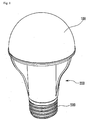
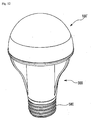
- Fig. 1 is a top perspective view of a lighting device according to a first embodiment.
- Fig. 2 is a bottom perspective view of the lighting device shown in Fig. 1 .
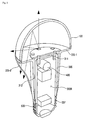
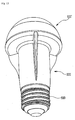
- Fig. 3 is an exploded perspective view of the lighting device shown in Fig. 1 .
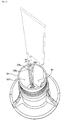
- Fig. 4 is an exploded perspective view of the lighting device shown in Fig. 2 .
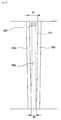
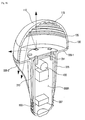
- Fig. 5 is a sectional perspective view of the lighting device shown in Fig. 1 .
- the lighting device may include a cover 100, a light source module 200, a heat sink 300, a power supply unit 400, and a base 500.
- a cover 100 a light source module 200
- a heat sink 300 a heat sink 300
- a power supply unit 400 a power supply unit 400
- the cover 100 has a hemispherical shape or a bulb shape.
- the cover 100 has an empty interior and a partial opening 100G.
- the hemispherical shape includes a shape similar to the hemisphere as well as a geometric hemisphere.
- An inner diameter of the cover 100 may become greater toward a lower portion from an upper portion of the cover 100.
- the cover 100 is optically coupled to the light source module 200. Specifically, the cover 100 may reflect, transmit or diffuse light emitted from the light source module 200.
- the cover 100 is coupled to the heat sink 300. Specifically, the cover 100 may be coupled to a second heat radiation part 330 of the heat sink 300. The lower portion of the cover 100 may be coupled to an outer portion 335 of the second heat radiation part 330 of the heat sink 300. Due to the coupling of the cover 100 and the heat sink 300, the light source module 200 is isolated from the outside. Therefore, the light source module 200 can be protected from external impurities or water.
- the cover 100 has an outer surface and an inner surface.
- the inner surface may reflect a part of the light from the light source module 200 and transmit the rest of the light.
- the inner surface of the cover 100 may reflect a part of light from a light emitting device 230 of the light source module 200 toward the outer portion 335 of the second heat radiation part 330 of the heat sink 300.
- the cover 100 may have a predetermined light diffusion rate.
- the cover 100 has a predetermined light diffusion rate (or an optical diffusion material), user's glare can be reduced.
- the cover 100 may be formed of any one of glass, plastic, polypropylene (PP), and polyethylene (PE).
- the cover 100 may be manufactured by a blow molding process.
- the light source module 200 is disposed on the heat sink 300 and includes the light emitting device 230 emitting predetermined light toward the cover 100. More specifically, the light source module 200 may include a substrate 210 and the light emitting device 230 disposed on the substrate 210.
- the substrate 210 may be formed by printing a circuit pattern on an insulator.
- the substrate 210 may include a printed circuit board (PCB), a metal core PCB, a flexible PCB, a ceramic PCB and the like.
- PCB printed circuit board
- metal core PCB metal core PCB
- flexible PCB flexible PCB
- ceramic PCB ceramic PCB
- the substrate 210 may be formed by printing a predetermined circuit pattern on a transparent or opaque resin.
- the resin may be a thin insulating sheet having the circuit pattern.
- the substrate 210 may have a circular plate shape. However, there is no limit to this.
- the substrate 210 may have a polygonal plate shape or an elliptical plate shape.
- the substrate 210 may be disposed on an upper portion 311 of a first heat radiation part 310 and on the outer portion 335 of the second heat radiation part 330. Specifically, a central portion of the substrate 210 may be disposed on a top surface of the upper portion 311 of the first heat radiation part 310, and the rest portion other than the central portion may be disposed on an outer circumferential portion 335-1 of the outer portion 335 of the second heat radiation part 330.
- the shape of the substrate 210 may correspond to the shape of the upper portion 311 of the first heat radiation part 310 of the heat sink 300.
- a diameter of the substrate 210 may be larger than that of the upper portion 311 of the first heat radiation part 310.
- a rear light distribution performance of the lighting device according to the first embodiment can be improved. Specifically, if the diameter of the substrate 210 is less than that of the upper portion 311, a part of light reflected by the cover 100 may be blocked by the upper portion 311 incapable of transmitting the light. This may cause the rear light distribution performance of the lighting device to be degraded. Therefore, it is preferred that the diameter of the substrate 210 be larger than that of the upper portion 311.
- the surface of the substrate 210 may be coated with a material capable of efficiently reflecting light or may be coated with a color, for example, white, silver and the like.
- the substrate 210 having the surface made of such a reflective material is able to reflect light incident thereon to the cover 100 again.
- the substrate 210 may have a first hole H1 allowing the substrate 210 to be coupled to the power supply unit 400. Specifically, this will be described with reference to Figs. 6 to 8 .
- Figs. 6 and 7 are perspective views showing a state where the light source module 200 and the power supply unit 400 shown in Fig. 3 have been coupled to each other.
- Fig. 8 is a conceptual diagram for describing an electrical connection between a substrate 210 and an extension part 450 which are shown in Figs. 3 and 4 .
- the substrate 210 has the first hole H1.
- the extension part 450 of the power supply unit 400 is disposed in the first hole H1.
- a height D1 from a top surface of the substrate 210 to the end of the extension part 450 which has passed through the first hole H1 of the substrate 210 may be from 1.5 mm to 2.0 mm. If the D1 is less than 1.5 mm, it is difficult to electrically connect the substrate 210 and the extension part 450, so that poor contact may occur between the substrate 210 and the extension part 450. Specifically, the electrical connection between the substrate 210 and the extension part 450 can be performed by soldering.
- a terminal 211 of the substrate 210 and a terminal 451 of the extension part 450 are required to contact with a soldering portion 700.
- the D1 is less than 1.5 mm, it is difficult for the terminal 451 of the extension part 450 to sufficiently contact with the soldering portion 700. In this case, the poor contact may occur between the substrate 210 and the extension part 450. Therefore, it is recommended that the D1 should be greater than 1.5 mm.
- the D1 is greater than 2.0 mm, a dark portion may be generated at the time of driving the light source module 200. Specifically, the dark portion may be generated in the vicinity of the extension part 450. The dark portion may degrade an optical efficiency of the lighting device and give an unpleasant appearance to users. Therefore, it is recommended that the D1 should be than 2.0 mm.
- the shape of the first hole H1 may correspond to the shape of the extended substrate 450.
- the diameter of the first hole H1 may be larger than the diameter of the extended substrate 450. That is, the size of the first hole H1 may be so large that the extended substrate 450 is inserted into the first hole H1. Therefore, the extended substrate 450 inserted into the first hole H1 may not contact with the substrate 210.
- an interval D2 between the substrate 210 and the extended substrate 450 may be greater than 0 and equal to or less than 0.2 mm. If the D2 is 0, the it may be difficult to insert the extended substrate 450 into the first hole H1 of the substrate 210, and an unintended electrical short-circuit may occur between the extended substrate 450 and the substrate 210.
- soldering materials may pass through the first hole H1 and flow down to a support plate 410 while performing the soldering process.
- a printed circuit formed in the support plate 410 may be electrically short-circuited by the soldering materials, and it may be difficult to accurately place the extended substrate 450 at a point where the extended substrate 450 is expected to be disposed in the first hole H1. Therefore, it is recommended that the D2 should be greater than 0 and equal to or less than 0.2 mm.
- the substrate 210 may have a second hole H2 for fixing the substrate 210 to the heat sink 300.
- a coupling means like a screw, passes through the second hole H2 of the substrate 210 and is inserted sequentially into a fourth hole H4 and a sixth hole H6 of the heat sink 300, thereby fixing the substrate 210 to the heat sink 300.
- a plurality of the light emitting devices 230 may be disposed on one side (or top surface) of the substrate 210. Specifically, the plurality of the light emitting devices 230 may be disposed radially on the one side of the substrate 210.
- the light emitting device 230 may be a light emitting diode chip emitting red, green and blue light or a light emitting diode chip emitting ultraviolet light.
- the light emitting diode chip may have a lateral type or vertical type.
- the light emitting device 230 may be a high-voltage (HV) LED package.
- a HV LED chip within the HV LED package is driven by a DC power supplier and is turned on at a voltage higher than 20V.
- the HV LED package has a high power consumption of about 1W.
- a conventional common LED chip is turned on at a voltage of 2V to 3V. Since the light emitting device 230 which is the HV LED package has the high power consumption of about 1W, the performance equivalent to or similar to that of the conventional common LED chip can be obtained only by a small number of the light emitting devices 230, so that it is possible to reduce the production cost of the lighting device according to the embodiment.
- a lens (not shown) may be disposed on the light emitting device 230.
- the lens (not shown) is disposed to cover the light emitting device 230.
- the lens (not shown) is able to adjust the orientation angle or direction of the light emitted from the light emitting device 230.
- the lens (not shown) has a hemispherical shape and may be formed of a light-transmitting resin such as a silicone resin or an epoxy resin without an empty space.
- the light-transmitting resin may include a wholly or partially distributed phosphor.
- the phosphor included in the light-transmitting resin may include at least one of garnet based phosphor (YAG, TAG), silicate based phosphor, nitride based phosphor and oxynitride based phosphor.
- an addition ratio of the color of the phosphor may be formed such that the green phosphor is more used than the red phosphor, and the yellow phosphor is more used than the green phosphor.
- the garnet based phosphor (YAG), the silicate based phosphor and the oxynitride based phosphor may be used as the yellow phosphor.
- the silicate based phosphor and the oxynitride based phosphor may be used as the green phosphor.
- the nitride based phosphor may be used as the red phosphor.
- the light-transmitting resin may be mixed with various kinds of the phosphors or may be configured by a layer including the red phosphor, a layer including the green phosphor and a layer including the yellow phosphor, which are formed separately from each other.
- the light source module 200 is disposed on the heat sink 300.
- the heat sink 300 may receive heat radiated from the light source module 200 and radiate the heat.
- the power supply unit 400 is disposed in the heat sink 300.
- the heat sink 300 may receive heat radiated from the power supply unit 400 and radiate the heat.
- the heat sink 300 may include the first heat radiation part 310 and the second heat radiation part 330.
- the first heat radiation part 310 may directly receive the heat from the light source module 200 and radiate the heat.
- the second heat radiation part 330 may transmit a part of the light reflected from the cover 100 and outwardly emit the light.
- the material of the first heat radiation part 310 may be different from that of the second heat radiation part 330.
- the first heat radiation part 310 may be formed of a material incapable of transmitting the light, that is, a material without an optical transmittance
- the second heat radiation part 330 may be formed of a material having a predetermined optical transmittance.
- the second heat radiation part 330 is formed of a material having an optical transmittance, a part of the light reflected from the cover 100 can be transmitted outwardly. Accordingly, the rear light distribution performance of the lighting device according to the first embodiment can be improved, and a light distribution angle of the lighting device according to the first embodiment can be increased. Also, the rear light distribution specifications (more than 5 % of total flux at 270° to 360° in C 90-270 ) of Energy Star can be satisfied.
- the material of the second heat radiation part 330 may be polycarbonate (PC), Poly-dimethyl cyclohexane terephthalate (PCT) and the like.
- PC polycarbonate
- PCT Poly-dimethyl cyclohexane terephthalate
- the material of the second heat radiation part 330 is not limited to what is mentioned above. Any material having a predetermined optical transmittance can be used as the material of the second heat radiation part 330.
- the power supply unit 400 disposed within the first heat radiation part 310 is not visible from the outside, aesthetic effect can be obtained.
- the first heat radiation part 310 may be formed of a non-insulating material
- the second heat radiation part 330 may be formed of an insulating material.
- the first heat radiation part 310 formed of the non-insulating material is able to quickly radiate the heat emitted from the light source module 200.
- the outer surface of the heat sink 300 becomes insulating due to the second heat radiation part 330 formed of the insulating material, thereby improving a withstand voltage characteristic of the lighting device and protecting a user from electrical energy. Since the second heat radiation part 330 encloses the power supply unit 400, the power supply unit 400 can be electrically protected.
- the first heat radiation part 310 may be formed of a metallic material such as aluminum, copper, magnesium and the like
- the second heat radiation part 330 may be formed of a resin material such as Polycarbonate (PC), Poly-dimethyl cyclohexane terephthalate (PCT), Acrylonitrile (AN), Butadiene (BD) and styrene (SM) (ABS), and the like.
- the resin-made second heat radiation part 330 may include a heat radiating filler.
- the heat radiating filler may include at least one of metal powder, ceramic, carbon fiber, graphene, and a carbon nanotube.
- a first thermal conductivity (W/(mk) or W/m°C) of the material constituting the first heat radiation part 310 may be greater than a second thermal conductivity of the material constituting the second heat radiation part 330. Since the light source module 200 is disposed closer to the first heat radiation part 310 than to the second heat radiation part 330, when the thermal conductivity of the first heat radiation part 310 is greater than the thermal conductivity of the second heat radiation part 330, it is advantageous for the improvement of heat radiation performance.
- the first heat radiation part 310 may be formed of aluminum having a high thermal conductivity
- the second heat radiation part 330 may be formed of polycarbonate (PC) or Poly-dimethyl cyclohexane terephthalate (PCT) having a thermal conductivity less than that of the first heat radiation part 310.
- the first heat radiation part 310 is not limited to the aluminum
- the second heat radiation part 330 is not limited to the PC.
- the light source module 200 is disposed on the first heat radiation part 310. Specifically, the substrate 210 and the light emitting devices 230 of the light source module 200 may be disposed on the upper portion 311 of the first heat radiation part 310.
- the first heat radiation part 310 may have a receiver 310R receiving the power supply unit 400 and an inner portion 331 of the second heat radiation part 330.
- the first heat radiation part 310 may include the upper portion 311 and a lower portion 313.
- the upper portion 311 and the lower portion 313 may define the receiver 310R.
- the upper portion 311 may have a flat plate shape.
- the substrate 210 and the light emitting devices 230 of the light source module 200 are disposed on the top surface of the upper portion 311, so that the upper portion 311 receives directly the heat from the light source module 200.
- the upper portion 311 may radiate the heat received from the light source module 200 to the outside or transfer to the lower portion 313.
- the top surface of the upper portion 311 may be disposed on the same plane with a top surface 355-1 of the outer portion 335 of the second heat radiation part 330.
- the substrate 210 can be stably disposed even though the size of the substrate 210 of the light source module 200 becomes larger than that of the top surface of the upper portion 311.
- the shape of the upper portion 311 is not limited to the flat plate shape.
- the shape of the upper portion 311 may be a plate shape of which a portion, especially, the central portion is upwardly or downwardly convex or may be a hemispherical shape.
- the upper portion 311 may have various shapes such as a circular shape, an elliptical shape or the like.
- the shape of the upper portion 311 may correspond to the shape of the substrate 210. Specifically, the upper portion 311 and the substrate 210 may have a circular shape. The diameter of the upper portion 311 may be less than that of the substrate 210. When the diameter of the upper portion 311 is less than that of the substrate 210, the rear light distribution performance of the lighting device according to the first embodiment can be enhanced. Specifically, unlike the second heat radiation part 330, the first heat radiation part 310 including the upper portion 311 is formed of a material without an optical transmittance.
- the diameter of the upper portion 311 is greater than that of the substrate 210, a part of the light reflected from the cover 100 is blocked by the upper portion 311, so that the rear light distribution performance of the lighting device according to the first embodiment may be degraded. Accordingly, it is preferred that the diameter of the upper portion 311 should be less than that of the substrate 210.
- the upper portion 3112 may have a third hole H3 through which the extension part 450 of the power supply unit 400 passes.
- the upper portion 311 may have the fourth hole H4 for fixing the first heat radiation part 310 to the second heat radiation part 330.
- a coupling means like a screw may pass through the fourth hole H4 and be inserted into the sixth hole H6 of the second heat radiation part 330.
- the upper portion 311 may be disposed on the inner portion 331 of the second heat radiation part 330. Specifically, the upper portion 311 may be disposed on a top surface of the second heat radiation part 330.
- a heat transfer means may be disposed between the upper portion 311 and the substrate 210 of the light source module 200 in order to quickly conduct the heat from the light source module 200 to the upper portion 311.
- the heat transfer means may be a heat radiating plate (not shown) or a thermal grease.
- the lower portion 313 may be disposed within the second heat radiation part 330. Specifically, the lower portion 313 may be disposed in a first receiver 333 of the second heat radiation part 330.
- the metallic lower portion 313 does not form the appearance of the lighting device. Accordingly, it is possible to protect users from electrical energy generated from the power supply unit 400. Since a heat sink of an existing lighting device is fully formed of a metallic material and the outer surface of the existing lighting device is formed of a metallic material, electrical energy caused by an inner power supply unit might affect the user. Therefore, by disposing the lower portion 313 in the first receiver 333 of the second heat radiation part 330, it is possible to prevent electrical accidents caused by the power supply unit 400.
- the lower portion 313 may be disposed between the inner portion 331 and the outer portion 335 of the second heat radiation part 330.
- the metallic lower portion 313 does not form the appearance of the lighting device according to the first embodiment. Accordingly, it is possible to protect users from electrical energy generated from the power supply unit 400.
- the lower portion 313 may have a tubular shape with an empty interior or may have a pipe shape. Specifically, the lower portion 313 may have any one of a cylindrical shape, an elliptical tubular shape and a polygonal box shape.
- the tubular shaped-lower portion 313 may have a constant diameter. Specifically, the diameter of the lower portion 313 may be constant from the top to the bottom of the lower portion 313. With the constant diameter of the lower portion 313 in manufacturing the lighting device according to the first embodiment, it may be possible to easily couple and separate the first heat radiation part 310 to and from the second heat radiation part 330.
- the lower portion 313 may have a predetermined length along the longitudinal direction of the second heat radiation part 330.
- the length of the lower portion 313 may extend from the top to the bottom of the second heat radiation part 330 or may extend from the top to the middle of the second heat radiation part 330. Therefore, the length of the lower portion 313 is not limited to what is shown in the drawings.
- the heat radiation performance may be enhanced with the increase of the length of the lower portion 313.
- a fin structure or an embossed structure may be included on at least one of the outer surface and the inner surface of the lower portion 313.
- the surface area of the lower portion 313 itself is increased, so that the heat radiating area is increased. As a result, the heat radiation performance of the heat sink 300 can be improved.
- the upper portion 311 and the lower portion 313 may be integrally formed with each other.
- it may mean that the individual upper portion 311 and the individual lower portion 313 are not connected by welding or bonding them, but the upper portion 311 and the lower portion 313 are connected as one to each other without being physically separated.
- the contact resistance between the upper portion 311 and the lower portion 313 is close to 0. Therefore, a heat transfer rate from the upper portion 311 to the lower portion 313 is higher than that when the upper portion 311 and the lower portion 313 are not integrally formed with each other.
- a process of coupling them for example, a press processing and the like, is not required, so that the cost in the manufacturing process can be reduced.
- the second heat radiation part 330 together with the cover 100, may form the appearance of the lighting device according to the embodiment and may receive the first heat radiation part 310 and the power supply unit 400.
- the first heat radiation part 310 is disposed within the second heat radiation part 330.
- the second heat radiation part 330 may include the first receiver 330 receiving the lower portion 313.
- the first receiver 333 may receive the upper portion 311 of the first heat radiation part 310 as well.
- the first receiver 333 is formed between the inner portion 331 and the outer portion 335 of the second heat radiation part 330, and may have a predetermined depth corresponding to the length of the lower portion 313.
- the second heat radiation part 330 may include a second receiver 330R receiving the power supply unit 400.
- the second receiver 330R is formed of a non-insulating resin material. Therefore, the power supply unit 400 received in the second receiver 330R can be used as a non-insulating PSU.
- the manufacturing cost of the non-insulating PSU is lower than that of an insulating PSU, so that the manufacturing cost of the lighting device can be reduced.
- the second heat radiation part 330 may include the inner portion 331, the outer portion 335, and a connection portion 337.
- the inner portion 331 of the second heat radiation part 330 is disposed in the receiver 310R of the first heat radiation part 310.
- the inner portion 331 of the second heat radiation part 330 may have a shape corresponding to the shape of the receiver 310R of the first heat radiation part 310.
- the substrate 210 of the light source module 200 is disposed on the top surface of the inner portion 331.
- the inner portion 331 may have the second receiver 330R receiving the power supply unit 400.
- the inner portion 331 may have a fifth hole H5 through which the extension part 450 of the power supply unit 400 disposed in the second receiver 330R passes. Also, the inner portion 331 may have the sixth hole H6 for fixing the substrate 210 and the first heat radiation part 310 to the second heat radiation part 330.
- the outer portion 335 of the second heat radiation part 330 encloses the first heat radiation part 310.
- the outer portion 335 of the second heat radiation part 330 may have a shape corresponding to the appearance of the first heat radiation part 310. Therefore, the inner portion 331 of the second heat radiation part 330, the first heat radiation part 310, and the outer portion 335 of the second heat radiation part 330 may have shapes corresponding to each other.
- the outer portion 335 may include the outer circumferential portion 335-1.
- the outer circumferential portion 335-1 may extend outwardly from the top of the outer portion 335.
- the top surface of the outer circumferential portion 335-1 may be disposed on the same plane with the top surface of the inner portion 331.
- the edge of the outer circumferential portion 335-1 is coupled to the end of the cover 100.
- the substrate 210 may be disposed on the top surface of the outer circumferential portion 335-1.
- the outer circumferential portion 335-1 may transmit at least a part of the light from the cover 100 and reflect the rest of the light to the cover 100 again. Since the outer circumferential portion 335-1 transmits the light, the lighting device is able to emit the light backward. Therefore, the rear light distribution performance of the lighting device according to the first embodiment can be improved.
- the outer portion 335 may have a fin 335-3.
- the fin 335-3 increases the surface area of the outer portion 335 of the second heat radiation part 330, so that the heat radiation performance of the heat sink 300 can be improved.
- the fin 335-3 increases the thickness of the outer portion 335, the light is not able to transmit through the fin 335-3, so that a dark portion may be generated in the fin 335-3. Therefore, it is recommended that the number of the fins 335-3 should be as small as possible, specifically, should be from 2 to 4.
- connection portion 337 of the second heat radiation part 330 may be formed of an insulating material and connected to the lower portions of the inner portion 331 and the outer portion 335.
- the connection portion 337 is coupled the base 500.
- the connection portion 337 may have a screw thread corresponding to a screw groove formed in the base 500.
- the connection portion 337, together with the inner portion 331, may form the second receiver 330R.
- connection portion 337 is coupled to the power supply unit 400, and thereby fixing the power supply unit 400 within the second receiver 330R.
- this will be described with reference to Fig. 9 .
- Fig. 9 is a view for describing a coupling structure between the connection portion 337 and the power supply unit 400.
- connection portion 337 has a coupling recess 337h.
- the coupling recess 337h has a predetermined diameter allowing a protrusion 470 of the support plate 410 to be inserted into the coupling recess 337h.
- the protrusion 470 may be formed in accordance with the number of the protrusions 470 of the support plate 410.
- the support plate 410 of the power supply unit 400 has the protrusion 470 which is coupled to the coupling recess 337h of the connection portion 337.
- the protrusion 470 may extend outwardly from both corners of the lower portion of the support plate 410.
- the protrusion 470 has a shape in such manner that it is easy for the support plate 410 to be received in the second receiver 330R and it is hard for the support plate 410 to come out of the second receiver 330R.
- the protrusion 470 may have a hook shape.
- the first receiver 333 of the second heat radiation part 330 is formed between the inner portion 331 and the outer portion 335 of the second heat radiation part 330, and receives the lower portion 313 of the first heat radiation part 310.
- the first receiver 333 may have a predetermined depth as much as the length of the lower portion 313 of the first heat radiation part 310.
- the first receiver 333 does not completely separate the inner portion 331 and the outer portion 335. That is, it is intended that the first receiver 333 is not formed between the lower portion of the inner portion 331 and the lower portion of the outer portion 335, so that the inner portion 331 and the outer portion 335 may be connected to each other.
- the first heat radiation part 310 may be coupled to the second heat radiation part 330. Specifically, after the first heat radiation part 310 is inserted into the first receiver 333 of the second heat radiation part 330, the first heat radiation part 310 and the second heat radiation part 330 may be coupled to each other through a bonding process or a coupling process.
- first heat radiation part 310 and the second heat radiation part 330 are integrally formed with each other. Also, the mutually coupled first and second heat radiation parts 310 and 330 may be limited to separate from each other. Specifically, the first heat radiation part 310 and the second heat radiation part 330 are in a state of being stuck together by a predetermined process. Therefore, the first heat radiation part 310 and the second heat radiation part 330 are difficult to separate.
- first heat radiation part 310 and the second heat radiation part 330 have been separated in Figs. 3 to 4 for the sake of convenience of the description.
- first heat radiation part 310 and the second heat radiation part 330 are integrally formed with each other or limited to separate from each other does not mean that they are not separated by any force, but means that it is possible to separate them by a predetermined force relatively greater than the force of human, for example, a mechanical force, and means that it is difficult to return to the previous state of having been coupled if the first heat radiation part 310 and the second heat radiation part 330 are separated from each other by the predetermined force.
- a contact resistance between the metallic first heat radiation part 310 and the resin made-second heat radiation part 330 may be less than a contact resistance in a case where the first heat radiation part 310 and the second heat radiation part 330 are not integrally formed with each other. Thanks to the reduced contact resistance, it is possible to obtain a heat radiation performance same as or similar to that of the conventional heat sink (entirely formed of a metallic material).
- first and second heat radiation parts 310 and 330 are integrally formed, the breakage and damage of the second heat radiation part 330 caused by external impact can be more reduced than when the first heat radiation part 310 and the second heat radiation part 330 are not integrally formed with each other.
- An insert injection process may be used to integrally form the first heat radiation part 310 and the second heat radiation part 330.
- the insert injection process is formed as follows. After, the previously manufactured first heat radiation part 310 is put into a mold (frame) for molding the second heat radiation part 330, a material constituting the second heat radiation part 330 is molten and put into the mold, and then is injected.
- the power supply unit 400 may include the support plate 410 and a plurality of parts 430.
- the support plate 410 mounts the plurality of parts 430.
- the support plate 410 may receive a power signal supplied through the base 500 and may have a printed pattern through which a predetermined power signal is supplied to the light source module 200.
- the support plate 410 may have a quadrangular plate shape.
- the support plate 410 is received in the second receiver 330R of the second heat radiation part 330. Specifically, this will be described with reference to Figs. 10 to 11 .
- Figs. 10 to 11 are views for describing a coupling structure between the support plate 410 and the heat sink 300.
- the second heat radiation part 330 may include a first and a second guides 338a and 338b which guide both sides of one edge of the support plate 410 respectively.
- the first and second guides 338a and 338b are disposed within the second receiver 330R of the second heat radiation part 330.
- the first and second guides 338a and 338b have a predetermined length toward the bottom surface of the second receiver 330R from the entrance of the second receiver 330R.
- the first and second guides 338a and 338b may protrude upwardly from the inner surface of the second heat radiation part 330 which forms the second receiver 330R.
- a guide recess 338g into which one side of the support plate 410 is inserted may be formed between the first guide 338a and the second guide 338b.
- An interval between the first guide 338a and the second guide 338b may be reduced toward the inside of the second receiver 330R (W1>W2).
- a diameter of the guide recess 338g may be reduced toward the inside of the second receiver 330R (W1>W2).
- the interval W1 between the first guide 338a and the second guide 338b should be greater than a value obtained by adding 1 mm to the thickness of the support plate 410. In other words, it is recommended that an interval between the first guide 338a and one surface of the support plate 410 should be greater than 0.5 mm.
- the interval W2 between the first guide 338a and the second guide 338b should be greater than the thickness of the support plate 410 and less than a value obtained by adding 0.1 mm to the thickness of the support plate 410. In other words, it is recommended that the interval between the first guide 338a and one surface of the support plate 410 should be greater than 0.05 mm.
- the coupling recess 337h into which the protrusion 470 of the support plate 410 is inserted is formed between the first guide 338a and the second guide 338b. Since the coupling recess 337h is formed between the first guide 338a and the second guide 338b, the support plate 410 can be disposed at a more accurate position and prevented from being separated.
- the support plate 410 may include the extended substrate 450.
- the extended substrate 450 extends outwardly from the top of the support plate 410.
- the extended substrate 450 passes through the fifth hole H5 of the heat sink 300 and the first hole H1 of the substrate 210, and then is electrically connected to the substrate 210 through the soldering process.
- the extension part 450 may be designated as an extended substrate.
- the support plate 410 may include the protrusion 470.
- the protrusion 470 extends outwardly from both corners of the lower portion of the support plate 410.
- the protrusion 470 is coupled to the connection portion 337 of the heat sink 300.
- the plurality of the parts 430 are mounted on the support plate 410.
- the plurality of the parts 430 may include, for example, a DC converter converting AC power supply supplied by an external power supply into DC power supply, a driving chip controlling the driving of the light source module 200, and an electrostatic discharge (ESD) protective device for protecting the light source module 200.
- ESD electrostatic discharge
- the power supply unit 400 may be the non-insulating PSU. If the power supply unit 400 is the non-insulating PSU, the manufacturing cost of the lighting device can be reduced.
- the base 500 is coupled to the connection portion 337 of the heat sink 300 and is electrically connected to the power supply unit 400.
- the base 500 transmits external AC power to the power supply unit 400.
- the base 500 may have the same size and shape as those of the base of a conventional incandescent bulb. For this reason, the lighting device according to the embodiment can take the place of the conventional incandescent bulb.
- the heat sink of the lighting device according to the embodiment also emits predetermined light. Therefore, without necessities of vertically disposing the light source module and of disposing a separate lens on the light source module for the purpose of the rear light distribution, the lighting device according to the embodiment is able to obtain the rear light distribution. Further, the light distribution angle of the lighting device according to the embodiment is greater than that of the conventional heat sink.
- Fig. 12 is a top perspective view of a lighting device according to a second embodiment.
- Fig. 13 is a bottom perspective view of the lighting device shown in Fig. 12 .
- Fig. 14 is an exploded perspective view of the lighting device shown in Fig. 12 .
- Fig. 15 is an exploded perspective view of the lighting device shown in Fig. 13 .
- Fig. 16 is a sectional perspective view of the lighting device shown in Fig. 12 .
- the lighting device may include a cover 100', the light source module 200, the heat sink 300, the power supply unit 400, and the base 500.
- the light source module 200, the heat sink 300, the power supply unit 400, and the base 500 are the same as the light source module 200, the heat sink 300, the power supply unit 400, and the base 500 of the lighting device according to the first embodiment shown in Figs. 1 to 11 , detailed descriptions of the light source module 200, the heat sink 300, the power supply unit 400, and the base 500 will be replaced by the foregoing descriptions.
- the cover 100' will be described in detail.
- the material of the cover 100' may be the same as that of the cover 100 shown in Figs. 1 to 11 .
- the cover 100' may include a first cover part 110 and a second cover part 130.
- the first cover part 110 may be designated as an upper portion
- the second cover part 130 may be designated a lower portion.
- the cover 100' is not limited to only the two of the first cover part 110 and the second cover part 130.
- the cover 100' may be comprised of three cover parts. Therefore, the cover 100' may be comprised of at least two cover parts.
- the first cover part 110 and the second cover part 130 are coupled to each other, thereby forming the cover 100' having a hemispherical shape or a bulb shape.
- the first cover part 110 and the second cover part 130 can be coupled to each other by an adhesive material or by a predetermined coupling structure, for example, a screw thread/screw groove structure, a hook structure, and the like.
- the first cover part 110 may be disposed on the substrate 210 of the light source module 200, and the second cover part 130 may be disposed around the substrate 210 of the light source module 200.
- the second cover part 130 may be disposed under the first cover part 110 and may be connected to an outer circumference of the first cover part 110.
- the diameter of the cover 100' becomes larger toward the lower portion of the second cover part 130 from the upper portion of the first cover part 110.
- the first cover part 110 may have an outer surface and an inner surface.
- An optical part 115 may be disposed on the inner surface of the first cover part 110.
- the optical part 115 may transmit a part of the light from the light emitting device 230 of the light source module 200 and reflect the rest of the light toward the outer circumferential portion 335-1 of the heat sink 300 or out of the top surface of the substrate 210.
- the optical part 115 is the inner surface itself of the first cover part 110 and may have a prism shape.
- the optical part 115 may be a prism sheet attached to the inner surface of the first cover part 110. Due to the optical part 115, the rear light distribution performance of the lighting device according to the second embodiment can be more improved than that of the lighting device according to the first embodiment.
- the optical part 115 may be disposed on the entire inner surface of the first cover part 110.
- the optical part 115 is not limited to this.
- the optical part 115 may be disposed on a portion of the inner surface of the first cover part 110.
- the optical part 115 is disposed on the entire or a portion of the inner surface of the first cover part 110 in accordance with the shape of the light source module 200 or the light distribution of the lighting device.
- the second cover part 130 is disposed under the first cover part 110 and has an inner surface and an outer surface.
- An optical part 135 may be disposed on the inner surface of the second cover part 130.
- the optical part 135 may transmit a part of the light from the light source module 200 and reflect the rest of the light toward the outer circumferential portion 335-1 of the heat sink 300 or out of the top surface of the substrate 210.
- the optical part 135 is the inner surface itself of the second cover part 130 and may have a prism shape.
- the optical part 135 may be a prism sheet attached to the inner surface of the second cover part 130. Due to the optical part 135, the rear light distribution performance of the lighting device according to the second embodiment can be more improved than that of the lighting device according to the first embodiment.
- the optical part 135 may be disposed on a portion of the inner surface of the second cover part 130.
- the optical part 135 is not limited to this.
- the optical part 135 may be disposed on the entire inner surface of the second cover part 130.
- the optical part 135 is disposed on a portion of or the entire inner surface of the second cover part 130 in accordance with the shape of the light source module 200 or the light distribution of the lighting device.
- the second cover part 130 may be coupled to the heat sink 300. Specifically, the lower portion of the second cover part 130 may be coupled to the outer circumferential portion 335-1 of the second heat radiation part 330 of the heat sink 300. Due to the coupling of the second cover part 130 and the heat sink 300, the light source module 200 is isolated from the outside. Therefore, the light source module 200 can be protected from external impurities or water.
- the material of the cover 100' may have an optical diffusion material for the purpose of preventing a user from feeling glare caused by the light emitted from the light source module 200.
- a light diffusion rate of the first cover part 110 may be higher than that of the second cover part 130.
- the rear light distribution performance of the lighting device according to the second embodiment can be more improved.
- the first cover part 110 is able to reflect more light from the light source module 200 than the second cover part 130. More specifically, referring to Fig. 5 , since the first cover part 110 is disposed on the light source module 200 and the second cover part 130 is disposed around the light source module 200, the first cover part 110 receives more light from the light source module 200 than the second cover part 130. Therefore, when the light diffusion rate of the first cover part 110 is higher than that of the second cover part 130, the amount of the light which is reflected to the heat sink 300 becomes increased, so that the rear light distribution performance of the lighting device according to the second embodiment can be more enhanced.
- the light diffusion rate of the first cover part 110 is higher than that of the second cover part 130, user's glare can be alleviated.
- the light emitting device 230 of the light source module 200 is an LED
- the LED irradiates strong light in a vertical axis. Therefore, the first cover part 110 disposed on the light source module 200 emits light stronger than that from the second cover part 130 disposed around the light source module 200. Accordingly, the light diffusion rate of the first cover part 110 becomes higher than that of the second cover part 130, so that it is possible to alleviate the user's glare.
- An optical reflectance of the first cover part 110 may be greater than that of the second cover part 130.
- the optical reflectance of the first cover part 110 is greater than that of the second cover part 130, the rear light distribution performance of the lighting device according to the second embodiment can be more enhanced and the user's glare can be alleviated.
- any reference in this specification to "one embodiment,” “an embodiment,” “example embodiment,” etc. means that a particular feature, structure, or characteristic described in connection with the embodiment is included in at least one embodiment of the invention.
- the appearances of such phrases in various places in the specification are not necessarily all referring to the same embodiment.
Description
- Embodiments may relate to a lighting device.
- A light emitting diode (LED) is an energy device for converting electric energy into light energy. Compared with an electric bulb, the LED has higher conversion efficiency, lower power consumption and a longer life span. As the advantages are widely known, more and more attentions are now paid to a lighting apparatus using the LED.
- The invention is a lighting device. The lighting device includes: a heat sink having an optical transmittance; a light source module including a substrate disposed on the heat sink and a light emitting device disposed on the substrate; and a cover which is disposed on the light source module and outwardly emits a part of light from the light source module. The cover has an inner surface which reflects a part of light from the light emitting device. The heat sink receives the light from the inner surface of the cover and outwardly emits a part of the received light. A lighting device with similar charcteristics is known from
DE 20 2012 009 071 . - The heat sink includes. a first heat radiation part including an upper portion on which the light source module is disposed, a lower portion connected to the upper portion, and a receiver; and a second heat radiation part including an inner portion which is disposed in the receiver of the first heat radiation part, and an outer portion which encloses the lower portion of the first heat radiation part. The second heat radiation part has the optical transmittance. The outer portion of the second heat radiation part emits outwardly a part of light incident from the inner surface of the cover.
- The outer portion of the second heat radiation part may include an outer circumferential portion which extends from a top of the outer portion and emits outwardly a part of light incident from the inner surface of the cover. A top surface of the first heat radiation part may be disposed on the same plane with a top surface of the outer circumferential portion.
- The first heat radiation part may be formed of a metallic material. The second heat radiation part may be formed of a resin material.
- The first heat radiation part may have a first thermal conductivity. The second heat radiation part may have a second thermal conductivity. The first thermal conductivity may be greater than the second thermal conductivity.
- The first heat radiation part and the second heat radiation part may be integrally formed with each other.
- The lighting device may further include a power supply unit supplying power to the light source module. The second heat radiation part may be formed of an insulating material. The inner portion of the second heat radiation part may include a receiver receiving the power supply unit.
- The lighting device may further include a base which is coupled to the heat sink. The power supply unit may include a support plate electrically connected to the base, and a plurality of parts disposed on the support plate. The second heat radiation part may further include a connection portion which is formed of an insulating material and allows the second heat radiation part to be connected to the base. The connection portion may have at least one hole. The support plate may have a protrusion which is inserted into the hole of the connection portion.
- The protrusion may have a hook structure.
- The power supply unit may include a support plate and a plurality of parts disposed on the support plate. The second heat radiation part may include a first guide and a second guide which are disposed in the receiver of the second heat radiation part and guide both sides of one edge of the support plate. An interval between the first guide and the second guide may be reduced toward a bottom surface of the receiver of the second heat radiation part from an entrance of the receiver of the second heat radiation part.
- The heat sink may have at least one fin. The number of the fins may be from 2 to 4.
- The cover may include a first cover part disposed on the substrate, and a second cover part connected to an outer circumference of the first cover part. An optical reflectance of the first cover part may be greater than an optical reflectance of the second cover part. The first cover part may include an optical part reflecting at least a part of light from the light emitting device out of a top surface of the substrate.
- The second cover part may further include an optical part reflecting at least a part of light from the light emitting device out of the top surface of the substrate.
- A light diffusion rate of the first cover part may be higher than a light diffusion rate of the second cover part.
- The optical part may have a prism shape.
- Arrangements and embodiments may be described in detail with reference to the following drawings in which like reference numerals refer to like elements and wherein:
-
Fig. 1 is a top perspective view of a lighting device according to a first embodiment; -
Fig. 2 is a bottom perspective view of the lighting device shown inFig. 1 ; -
Fig. 3 is an exploded perspective view of the lighting device shown inFig. 1 ; -
Fig. 4 is an exploded perspective view of the lighting device shown inFig. 2 ; -
Fig. 5 is a sectional perspective view of the lighting device shown inFig. 1 ; -
Figs. 6 and 7 are perspective views showing a state where alight source module 200 and apower supply unit 400 shown inFig. 3 have been coupled to each other; -
Fig. 8 is a conceptual diagram for describing an electrical connection between asubstrate 210 and anextension part 450 which are shown inFigs. 3 and4 ; -
Fig. 9 is a view for describing a coupling structure between aconnection portion 337 and thepower supply unit 400; -
Figs. 10 to 11 are views for describing a coupling structure between asupport plate 400 and aheat sink 300; -
Fig. 12 is a top perspective view of a lighting device according to a second embodiment; -
Fig. 13 is a bottom perspective view of the lighting device shown inFig. 12 ; -
Fig. 14 is an exploded perspective view of the lighting device shown inFig. 12 ; -
Fig. 15 is an exploded perspective view of the lighting device shown inFig. 13 ; and -
Fig. 16 is a sectional perspective view of the lighting device shown inFig. 12 . - A thickness or a size of each layer may be magnified, omitted or schematically shown for the purpose of convenience and clearness of description. The size of each component may not necessarily mean its actual size.
- It should be understood that when an element is referred to as being 'on' or "under" another element, it may be directly on/under the element, and/or one or more intervening elements may also be present. When an element is referred to as being 'on' or 'under', 'under the element' as well as 'on the element' may be included based on the element.
- An embodiment may be described in detail with reference to the accompanying drawings.
-
Fig. 1 is a top perspective view of a lighting device according to a first embodiment.Fig. 2 is a bottom perspective view of the lighting device shown inFig. 1 .Fig. 3 is an exploded perspective view of the lighting device shown inFig. 1 .Fig. 4 is an exploded perspective view of the lighting device shown inFig. 2 .Fig. 5 is a sectional perspective view of the lighting device shown inFig. 1 . - Referring to
Figs. 1 to 5 , the lighting device according to the first embodiment may include acover 100, alight source module 200, aheat sink 300, apower supply unit 400, and abase 500. Hereafter, the respective components will be described in detail. - The
cover 100 has a hemispherical shape or a bulb shape. Thecover 100 has an empty interior and apartial opening 100G. Here, it should be understood that the hemispherical shape includes a shape similar to the hemisphere as well as a geometric hemisphere. - An inner diameter of the
cover 100 may become greater toward a lower portion from an upper portion of thecover 100. - The
cover 100 is optically coupled to thelight source module 200. Specifically, thecover 100 may reflect, transmit or diffuse light emitted from thelight source module 200. - The
cover 100 is coupled to theheat sink 300. Specifically, thecover 100 may be coupled to a secondheat radiation part 330 of theheat sink 300. The lower portion of thecover 100 may be coupled to anouter portion 335 of the secondheat radiation part 330 of theheat sink 300. Due to the coupling of thecover 100 and theheat sink 300, thelight source module 200 is isolated from the outside. Therefore, thelight source module 200 can be protected from external impurities or water. - The
cover 100 has an outer surface and an inner surface. The inner surface may reflect a part of the light from thelight source module 200 and transmit the rest of the light. Particularly, the inner surface of thecover 100 may reflect a part of light from alight emitting device 230 of thelight source module 200 toward theouter portion 335 of the secondheat radiation part 330 of theheat sink 300. - When the
light emitting device 230 of thelight source module 200 is an LED, the LED irradiates strong light in a direction of a vertical axis. Therefore, thecover 100 may have a predetermined light diffusion rate. When thecover 100 has a predetermined light diffusion rate (or an optical diffusion material), user's glare can be reduced. - The
cover 100 may be formed of any one of glass, plastic, polypropylene (PP), and polyethylene (PE). - The
cover 100 may be manufactured by a blow molding process. - The
light source module 200 is disposed on theheat sink 300 and includes thelight emitting device 230 emitting predetermined light toward thecover 100. More specifically, thelight source module 200 may include asubstrate 210 and thelight emitting device 230 disposed on thesubstrate 210. - The
substrate 210 may be formed by printing a circuit pattern on an insulator. For example, thesubstrate 210 may include a printed circuit board (PCB), a metal core PCB, a flexible PCB, a ceramic PCB and the like. - The
substrate 210 may be formed by printing a predetermined circuit pattern on a transparent or opaque resin. Here, the resin may be a thin insulating sheet having the circuit pattern. - The
substrate 210 may have a circular plate shape. However, there is no limit to this. Thesubstrate 210 may have a polygonal plate shape or an elliptical plate shape. - The
substrate 210 may be disposed on anupper portion 311 of a firstheat radiation part 310 and on theouter portion 335 of the secondheat radiation part 330. Specifically, a central portion of thesubstrate 210 may be disposed on a top surface of theupper portion 311 of the firstheat radiation part 310, and the rest portion other than the central portion may be disposed on an outer circumferential portion 335-1 of theouter portion 335 of the secondheat radiation part 330. - The shape of the
substrate 210 may correspond to the shape of theupper portion 311 of the firstheat radiation part 310 of theheat sink 300. - A diameter of the
substrate 210 may be larger than that of theupper portion 311 of the firstheat radiation part 310. When the diameter of thesubstrate 210 is larger than that of theupper portion 311, a rear light distribution performance of the lighting device according to the first embodiment can be improved. Specifically, if the diameter of thesubstrate 210 is less than that of theupper portion 311, a part of light reflected by thecover 100 may be blocked by theupper portion 311 incapable of transmitting the light. This may cause the rear light distribution performance of the lighting device to be degraded. Therefore, it is preferred that the diameter of thesubstrate 210 be larger than that of theupper portion 311. - The surface of the
substrate 210 may be coated with a material capable of efficiently reflecting light or may be coated with a color, for example, white, silver and the like. Thesubstrate 210 having the surface made of such a reflective material is able to reflect light incident thereon to thecover 100 again. - The
substrate 210 may have a first hole H1 allowing thesubstrate 210 to be coupled to thepower supply unit 400. Specifically, this will be described with reference toFigs. 6 to 8 . -
Figs. 6 and 7 are perspective views showing a state where thelight source module 200 and thepower supply unit 400 shown inFig. 3 have been coupled to each other.Fig. 8 is a conceptual diagram for describing an electrical connection between asubstrate 210 and anextension part 450 which are shown inFigs. 3 and4 . - Referring to
Figs. 3 to 8 , thesubstrate 210 has the first hole H1. Theextension part 450 of thepower supply unit 400 is disposed in the first hole H1. - Here, as shown in
Fig. 8 , a height D1 from a top surface of thesubstrate 210 to the end of theextension part 450 which has passed through the first hole H1 of thesubstrate 210, that is to say, a length D1 of a portion of theextension part 450, which has passed through the first hole H1 of thesubstrate 210 may be from 1.5 mm to 2.0 mm. If the D1 is less than 1.5 mm, it is difficult to electrically connect thesubstrate 210 and theextension part 450, so that poor contact may occur between thesubstrate 210 and theextension part 450. Specifically, the electrical connection between thesubstrate 210 and theextension part 450 can be performed by soldering. For the sake of the soldering process, aterminal 211 of thesubstrate 210 and aterminal 451 of theextension part 450 are required to contact with asoldering portion 700. If the D1 is less than 1.5 mm, it is difficult for theterminal 451 of theextension part 450 to sufficiently contact with thesoldering portion 700. In this case, the poor contact may occur between thesubstrate 210 and theextension part 450. Therefore, it is recommended that the D1 should be greater than 1.5 mm. If the D1 is greater than 2.0 mm, a dark portion may be generated at the time of driving thelight source module 200. Specifically, the dark portion may be generated in the vicinity of theextension part 450. The dark portion may degrade an optical efficiency of the lighting device and give an unpleasant appearance to users. Therefore, it is recommended that the D1 should be than 2.0 mm. - The shape of the first hole H1 may correspond to the shape of the
extended substrate 450. Here, the diameter of the first hole H1 may be larger than the diameter of theextended substrate 450. That is, the size of the first hole H1 may be so large that theextended substrate 450 is inserted into the first hole H1. Therefore, theextended substrate 450 inserted into the first hole H1 may not contact with thesubstrate 210. In the first hole H1, an interval D2 between thesubstrate 210 and theextended substrate 450 may be greater than 0 and equal to or less than 0.2 mm. If the D2 is 0, the it may be difficult to insert theextended substrate 450 into the first hole H1 of thesubstrate 210, and an unintended electrical short-circuit may occur between theextended substrate 450 and thesubstrate 210. On the other hand, if the D2 is greater than 0.2 mm, soldering materials may pass through the first hole H1 and flow down to asupport plate 410 while performing the soldering process. In this case, a printed circuit formed in thesupport plate 410 may be electrically short-circuited by the soldering materials, and it may be difficult to accurately place theextended substrate 450 at a point where theextended substrate 450 is expected to be disposed in the first hole H1. Therefore, it is recommended that the D2 should be greater than 0 and equal to or less than 0.2 mm. - Referring back to
Figs. 3 to 5 , thesubstrate 210 may have a second hole H2 for fixing thesubstrate 210 to theheat sink 300. A coupling means like a screw, passes through the second hole H2 of thesubstrate 210 and is inserted sequentially into a fourth hole H4 and a sixth hole H6 of theheat sink 300, thereby fixing thesubstrate 210 to theheat sink 300. - A plurality of the
light emitting devices 230 may be disposed on one side (or top surface) of thesubstrate 210. Specifically, the plurality of thelight emitting devices 230 may be disposed radially on the one side of thesubstrate 210. - The
light emitting device 230 may be a light emitting diode chip emitting red, green and blue light or a light emitting diode chip emitting ultraviolet light. Here, the light emitting diode chip may have a lateral type or vertical type. - The
light emitting device 230 may be a high-voltage (HV) LED package. A HV LED chip within the HV LED package is driven by a DC power supplier and is turned on at a voltage higher than 20V. The HV LED package has a high power consumption of about 1W. For reference, a conventional common LED chip is turned on at a voltage of 2V to 3V. Since thelight emitting device 230 which is the HV LED package has the high power consumption of about 1W, the performance equivalent to or similar to that of the conventional common LED chip can be obtained only by a small number of thelight emitting devices 230, so that it is possible to reduce the production cost of the lighting device according to the embodiment. - A lens (not shown) may be disposed on the
light emitting device 230. The lens (not shown) is disposed to cover thelight emitting device 230. The lens (not shown) is able to adjust the orientation angle or direction of the light emitted from thelight emitting device 230. The lens (not shown) has a hemispherical shape and may be formed of a light-transmitting resin such as a silicone resin or an epoxy resin without an empty space. The light-transmitting resin may include a wholly or partially distributed phosphor. - When the
light emitting device 230 is a blue light emitting diode, the phosphor included in the light-transmitting resin may include at least one of garnet based phosphor (YAG, TAG), silicate based phosphor, nitride based phosphor and oxynitride based phosphor. - It is possible to create natural sunlight (white light) by including only yellow phosphor to the light-transmitting resin. Additionally, green phosphor or red phosphor may be further included in order to improve a color rendering index and to reduce a color temperature.
- When many kinds of fluorescent materials are mixed in the light-transmitting resin, an addition ratio of the color of the phosphor may be formed such that the green phosphor is more used than the red phosphor, and the yellow phosphor is more used than the green phosphor. The garnet based phosphor (YAG), the silicate based phosphor and the oxynitride based phosphor may be used as the yellow phosphor. The silicate based phosphor and the oxynitride based phosphor may be used as the green phosphor. The nitride based phosphor may be used as the red phosphor. The light-transmitting resin may be mixed with various kinds of the phosphors or may be configured by a layer including the red phosphor, a layer including the green phosphor and a layer including the yellow phosphor, which are formed separately from each other.
- The
light source module 200 is disposed on theheat sink 300. Theheat sink 300 may receive heat radiated from thelight source module 200 and radiate the heat. - The
power supply unit 400 is disposed in theheat sink 300. Theheat sink 300 may receive heat radiated from thepower supply unit 400 and radiate the heat. - The
heat sink 300 may include the firstheat radiation part 310 and the secondheat radiation part 330. The firstheat radiation part 310 may directly receive the heat from thelight source module 200 and radiate the heat. The secondheat radiation part 330 may transmit a part of the light reflected from thecover 100 and outwardly emit the light. - The material of the first
heat radiation part 310 may be different from that of the secondheat radiation part 330. Specifically, the firstheat radiation part 310 may be formed of a material incapable of transmitting the light, that is, a material without an optical transmittance, and the secondheat radiation part 330 may be formed of a material having a predetermined optical transmittance. When the secondheat radiation part 330 is formed of a material having an optical transmittance, a part of the light reflected from thecover 100 can be transmitted outwardly. Accordingly, the rear light distribution performance of the lighting device according to the first embodiment can be improved, and a light distribution angle of the lighting device according to the first embodiment can be increased. Also, the rear light distribution specifications (more than 5 % of total flux at 270° to 360° in C90-270) of Energy Star can be satisfied. - The material of the second
heat radiation part 330 may be polycarbonate (PC), Poly-dimethyl cyclohexane terephthalate (PCT) and the like. Here, the material of the secondheat radiation part 330 is not limited to what is mentioned above. Any material having a predetermined optical transmittance can be used as the material of the secondheat radiation part 330. - When the first
heat radiation part 310 is formed of a material without an optical transmittance, thepower supply unit 400 disposed within the firstheat radiation part 310 is not visible from the outside, aesthetic effect can be obtained. - The first
heat radiation part 310 may be formed of a non-insulating material, and the secondheat radiation part 330 may be formed of an insulating material. The firstheat radiation part 310 formed of the non-insulating material is able to quickly radiate the heat emitted from thelight source module 200. The outer surface of theheat sink 300 becomes insulating due to the secondheat radiation part 330 formed of the insulating material, thereby improving a withstand voltage characteristic of the lighting device and protecting a user from electrical energy. Since the secondheat radiation part 330 encloses thepower supply unit 400, thepower supply unit 400 can be electrically protected. - The first
heat radiation part 310 may be formed of a metallic material such as aluminum, copper, magnesium and the like, and the secondheat radiation part 330 may be formed of a resin material such as Polycarbonate (PC), Poly-dimethyl cyclohexane terephthalate (PCT), Acrylonitrile (AN), Butadiene (BD) and styrene (SM) (ABS), and the like. Here, the resin-made secondheat radiation part 330 may include a heat radiating filler. The heat radiating filler may include at least one of metal powder, ceramic, carbon fiber, graphene, and a carbon nanotube. - It is easier to form the external appearance of the resin-made second
heat radiation part 330 than to form the external appearance of a conventional metallic heat sink. Also, poor appearance caused by coating or anodizing the conventional heat sink does not occur in the resin-made secondheat radiation part 330. Also, an AC LED can be directly applied. Also, it is possible to reduce the weight and material cost of the entire lighting device. - A first thermal conductivity (W/(mk) or W/m°C) of the material constituting the first
heat radiation part 310 may be greater than a second thermal conductivity of the material constituting the secondheat radiation part 330. Since thelight source module 200 is disposed closer to the firstheat radiation part 310 than to the secondheat radiation part 330, when the thermal conductivity of the firstheat radiation part 310 is greater than the thermal conductivity of the secondheat radiation part 330, it is advantageous for the improvement of heat radiation performance. For example, the firstheat radiation part 310 may be formed of aluminum having a high thermal conductivity, and the secondheat radiation part 330 may be formed of polycarbonate (PC) or Poly-dimethyl cyclohexane terephthalate (PCT) having a thermal conductivity less than that of the firstheat radiation part 310. Here, the firstheat radiation part 310 is not limited to the aluminum, and the secondheat radiation part 330 is not limited to the PC. - The
light source module 200 is disposed on the firstheat radiation part 310. Specifically, thesubstrate 210 and thelight emitting devices 230 of thelight source module 200 may be disposed on theupper portion 311 of the firstheat radiation part 310. - The first
heat radiation part 310 may have areceiver 310R receiving thepower supply unit 400 and aninner portion 331 of the secondheat radiation part 330. - The first
heat radiation part 310 may include theupper portion 311 and alower portion 313. Theupper portion 311 and thelower portion 313 may define thereceiver 310R. - The
upper portion 311 may have a flat plate shape. Thesubstrate 210 and thelight emitting devices 230 of thelight source module 200 are disposed on the top surface of theupper portion 311, so that theupper portion 311 receives directly the heat from thelight source module 200. Theupper portion 311 may radiate the heat received from thelight source module 200 to the outside or transfer to thelower portion 313. - The top surface of the
upper portion 311 may be disposed on the same plane with a top surface 355-1 of theouter portion 335 of the secondheat radiation part 330. When the top surface of theupper portion 311 is disposed on the same plane with a top surface of the outer circumferential portion 335-1 of theouter portion 335, thesubstrate 210 can be stably disposed even though the size of thesubstrate 210 of thelight source module 200 becomes larger than that of the top surface of theupper portion 311. - The shape of the
upper portion 311 is not limited to the flat plate shape. For example, the shape of theupper portion 311 may be a plate shape of which a portion, especially, the central portion is upwardly or downwardly convex or may be a hemispherical shape. Also, theupper portion 311 may have various shapes such as a circular shape, an elliptical shape or the like. - The shape of the
upper portion 311 may correspond to the shape of thesubstrate 210. Specifically, theupper portion 311 and thesubstrate 210 may have a circular shape. The diameter of theupper portion 311 may be less than that of thesubstrate 210. When the diameter of theupper portion 311 is less than that of thesubstrate 210, the rear light distribution performance of the lighting device according to the first embodiment can be enhanced. Specifically, unlike the secondheat radiation part 330, the firstheat radiation part 310 including theupper portion 311 is formed of a material without an optical transmittance. Therefore, if the diameter of theupper portion 311 is greater than that of thesubstrate 210, a part of the light reflected from thecover 100 is blocked by theupper portion 311, so that the rear light distribution performance of the lighting device according to the first embodiment may be degraded. Accordingly, it is preferred that the diameter of theupper portion 311 should be less than that of thesubstrate 210. - The upper portion 3112 may have a third hole H3 through which the
extension part 450 of thepower supply unit 400 passes. - The
upper portion 311 may have the fourth hole H4 for fixing the firstheat radiation part 310 to the secondheat radiation part 330. A coupling means (not shown) like a screw may pass through the fourth hole H4 and be inserted into the sixth hole H6 of the secondheat radiation part 330. - The
upper portion 311 may be disposed on theinner portion 331 of the secondheat radiation part 330. Specifically, theupper portion 311 may be disposed on a top surface of the secondheat radiation part 330. - A heat transfer means may be disposed between the
upper portion 311 and thesubstrate 210 of thelight source module 200 in order to quickly conduct the heat from thelight source module 200 to theupper portion 311. Here, the heat transfer means may be a heat radiating plate (not shown) or a thermal grease. - The
lower portion 313 may be disposed within the secondheat radiation part 330. Specifically, thelower portion 313 may be disposed in afirst receiver 333 of the secondheat radiation part 330. When thelower portion 313 is disposed in thefirst receiver 333 of the secondheat radiation part 330, the metalliclower portion 313 does not form the appearance of the lighting device. Accordingly, it is possible to protect users from electrical energy generated from thepower supply unit 400. Since a heat sink of an existing lighting device is fully formed of a metallic material and the outer surface of the existing lighting device is formed of a metallic material, electrical energy caused by an inner power supply unit might affect the user. Therefore, by disposing thelower portion 313 in thefirst receiver 333 of the secondheat radiation part 330, it is possible to prevent electrical accidents caused by thepower supply unit 400. - The
lower portion 313 may be disposed between theinner portion 331 and theouter portion 335 of the secondheat radiation part 330. When thelower portion 313 is disposed between theinner portion 331 and theouter portion 335 of the secondheat radiation part 330, the metalliclower portion 313 does not form the appearance of the lighting device according to the first embodiment. Accordingly, it is possible to protect users from electrical energy generated from thepower supply unit 400. - The
lower portion 313 may have a tubular shape with an empty interior or may have a pipe shape. Specifically, thelower portion 313 may have any one of a cylindrical shape, an elliptical tubular shape and a polygonal box shape. The tubular shaped-lower portion 313 may have a constant diameter. Specifically, the diameter of thelower portion 313 may be constant from the top to the bottom of thelower portion 313. With the constant diameter of thelower portion 313 in manufacturing the lighting device according to the first embodiment, it may be possible to easily couple and separate the firstheat radiation part 310 to and from the secondheat radiation part 330. - The
lower portion 313 may have a predetermined length along the longitudinal direction of the secondheat radiation part 330. The length of thelower portion 313 may extend from the top to the bottom of the secondheat radiation part 330 or may extend from the top to the middle of the secondheat radiation part 330. Therefore, the length of thelower portion 313 is not limited to what is shown in the drawings. The heat radiation performance may be enhanced with the increase of the length of thelower portion 313. - A fin structure or an embossed structure (not shown) may be included on at least one of the outer surface and the inner surface of the
lower portion 313. When the fin or the embossed structure is included on thelower portion 313, the surface area of thelower portion 313 itself is increased, so that the heat radiating area is increased. As a result, the heat radiation performance of theheat sink 300 can be improved. - The
upper portion 311 and thelower portion 313 may be integrally formed with each other. In the present specification, it may mean that the individualupper portion 311 and the individuallower portion 313 are not connected by welding or bonding them, but theupper portion 311 and thelower portion 313 are connected as one to each other without being physically separated. When theupper portion 311 and thelower portion 313 are integrally formed with each other, the contact resistance between theupper portion 311 and thelower portion 313 is close to 0. Therefore, a heat transfer rate from theupper portion 311 to thelower portion 313 is higher than that when theupper portion 311 and thelower portion 313 are not integrally formed with each other. Also, when theupper portion 311 and thelower portion 313 are integrally formed with each other, a process of coupling them, for example, a press processing and the like, is not required, so that the cost in the manufacturing process can be reduced. - The second
heat radiation part 330, together with thecover 100, may form the appearance of the lighting device according to the embodiment and may receive the firstheat radiation part 310 and thepower supply unit 400. - The first
heat radiation part 310 is disposed within the secondheat radiation part 330. Specifically, the secondheat radiation part 330 may include thefirst receiver 330 receiving thelower portion 313. Here, thefirst receiver 333 may receive theupper portion 311 of the firstheat radiation part 310 as well. Thefirst receiver 333 is formed between theinner portion 331 and theouter portion 335 of the secondheat radiation part 330, and may have a predetermined depth corresponding to the length of thelower portion 313. - The second
heat radiation part 330 may include asecond receiver 330R receiving thepower supply unit 400. Here, unlike a receiver of the heat sink of a conventional lighting device, thesecond receiver 330R is formed of a non-insulating resin material. Therefore, thepower supply unit 400 received in thesecond receiver 330R can be used as a non-insulating PSU. The manufacturing cost of the non-insulating PSU is lower than that of an insulating PSU, so that the manufacturing cost of the lighting device can be reduced. - The second
heat radiation part 330 may include theinner portion 331, theouter portion 335, and aconnection portion 337. - The
inner portion 331 of the secondheat radiation part 330 is disposed in thereceiver 310R of the firstheat radiation part 310. In order that theinner portion 331 of the secondheat radiation part 330 is disposed in thereceiver 310R of the firstheat radiation part 310, theinner portion 331 of the secondheat radiation part 330 may have a shape corresponding to the shape of thereceiver 310R of the firstheat radiation part 310. - The
substrate 210 of thelight source module 200 is disposed on the top surface of theinner portion 331. - The
inner portion 331 may have thesecond receiver 330R receiving thepower supply unit 400. - The
inner portion 331 may have a fifth hole H5 through which theextension part 450 of thepower supply unit 400 disposed in thesecond receiver 330R passes. Also, theinner portion 331 may have the sixth hole H6 for fixing thesubstrate 210 and the firstheat radiation part 310 to the secondheat radiation part 330. - The
outer portion 335 of the secondheat radiation part 330 encloses the firstheat radiation part 310. Here, theouter portion 335 of the secondheat radiation part 330 may have a shape corresponding to the appearance of the firstheat radiation part 310. Therefore, theinner portion 331 of the secondheat radiation part 330, the firstheat radiation part 310, and theouter portion 335 of the secondheat radiation part 330 may have shapes corresponding to each other. - The
outer portion 335 may include the outer circumferential portion 335-1. The outer circumferential portion 335-1 may extend outwardly from the top of theouter portion 335. The top surface of the outer circumferential portion 335-1 may be disposed on the same plane with the top surface of theinner portion 331. The edge of the outer circumferential portion 335-1 is coupled to the end of thecover 100. Thesubstrate 210 may be disposed on the top surface of the outer circumferential portion 335-1. - As shown in
Fig. 5 , the outer circumferential portion 335-1 may transmit at least a part of the light from thecover 100 and reflect the rest of the light to thecover 100 again. Since the outer circumferential portion 335-1 transmits the light, the lighting device is able to emit the light backward. Therefore, the rear light distribution performance of the lighting device according to the first embodiment can be improved. - The
outer portion 335 may have a fin 335-3. The fin 335-3 increases the surface area of theouter portion 335 of the secondheat radiation part 330, so that the heat radiation performance of theheat sink 300 can be improved. However, since the fin 335-3 increases the thickness of theouter portion 335, the light is not able to transmit through the fin 335-3, so that a dark portion may be generated in the fin 335-3. Therefore, it is recommended that the number of the fins 335-3 should be as small as possible, specifically, should be from 2 to 4. - The
connection portion 337 of the secondheat radiation part 330 may be formed of an insulating material and connected to the lower portions of theinner portion 331 and theouter portion 335. Theconnection portion 337 is coupled thebase 500. Theconnection portion 337 may have a screw thread corresponding to a screw groove formed in thebase 500. Theconnection portion 337, together with theinner portion 331, may form thesecond receiver 330R. - The
connection portion 337 is coupled to thepower supply unit 400, and thereby fixing thepower supply unit 400 within thesecond receiver 330R. Hereafter, this will be described with reference toFig. 9 . -
Fig. 9 is a view for describing a coupling structure between theconnection portion 337 and thepower supply unit 400. - Referring to
Fig. 9 , theconnection portion 337 has acoupling recess 337h. Thecoupling recess 337h has a predetermined diameter allowing aprotrusion 470 of thesupport plate 410 to be inserted into thecoupling recess 337h. Theprotrusion 470 may be formed in accordance with the number of theprotrusions 470 of thesupport plate 410. - The
support plate 410 of thepower supply unit 400 has theprotrusion 470 which is coupled to thecoupling recess 337h of theconnection portion 337. Theprotrusion 470 may extend outwardly from both corners of the lower portion of thesupport plate 410. Theprotrusion 470 has a shape in such manner that it is easy for thesupport plate 410 to be received in thesecond receiver 330R and it is hard for thesupport plate 410 to come out of thesecond receiver 330R. For example, theprotrusion 470 may have a hook shape. - When the
protrusion 470 of thesupport plate 410 is coupled to thecoupling recess 337h of theconnection portion 337, it is hard for thesupport plate 410 to come out of thesecond receiver 330R, thereby firmly fixing thesupport plate 410 within thesecond receiver 330R. Therefore, a separate additional process, for example, a molding process of thepower supply unit 400 is not required, so that the manufacturing cost of the lighting device can be reduced. - Referring back to
Figs. 1 to 5 , thefirst receiver 333 of the secondheat radiation part 330 is formed between theinner portion 331 and theouter portion 335 of the secondheat radiation part 330, and receives thelower portion 313 of the firstheat radiation part 310. Thefirst receiver 333 may have a predetermined depth as much as the length of thelower portion 313 of the firstheat radiation part 310. Here, thefirst receiver 333 does not completely separate theinner portion 331 and theouter portion 335. That is, it is intended that thefirst receiver 333 is not formed between the lower portion of theinner portion 331 and the lower portion of theouter portion 335, so that theinner portion 331 and theouter portion 335 may be connected to each other. - After the first
heat radiation part 310 and the secondheat radiation part 330 are separately produced, the firstheat radiation part 310 may be coupled to the secondheat radiation part 330. Specifically, after the firstheat radiation part 310 is inserted into thefirst receiver 333 of the secondheat radiation part 330, the firstheat radiation part 310 and the secondheat radiation part 330 may be coupled to each other through a bonding process or a coupling process. - Meanwhile, the first
heat radiation part 310 and the secondheat radiation part 330 are integrally formed with each other. Also, the mutually coupled first and secondheat radiation parts heat radiation part 310 and the secondheat radiation part 330 are in a state of being stuck together by a predetermined process. Therefore, the firstheat radiation part 310 and the secondheat radiation part 330 are difficult to separate. Here, it is noted that the firstheat radiation part 310 and the secondheat radiation part 330 have been separated inFigs. 3 to 4 for the sake of convenience of the description. In the present specification, it should be understood that the fact that firstheat radiation part 310 and the secondheat radiation part 330 are integrally formed with each other or limited to separate from each other does not mean that they are not separated by any force, but means that it is possible to separate them by a predetermined force relatively greater than the force of human, for example, a mechanical force, and means that it is difficult to return to the previous state of having been coupled if the firstheat radiation part 310 and the secondheat radiation part 330 are separated from each other by the predetermined force. - When the first
heat radiation part 310 and the secondheat radiation part 330 are integrally formed with each other or limited to separate from each other, a contact resistance between the metallic firstheat radiation part 310 and the resin made-secondheat radiation part 330 may be less than a contact resistance in a case where the firstheat radiation part 310 and the secondheat radiation part 330 are not integrally formed with each other. Thanks to the reduced contact resistance, it is possible to obtain a heat radiation performance same as or similar to that of the conventional heat sink (entirely formed of a metallic material). Further, when the first and secondheat radiation parts heat radiation part 330 caused by external impact can be more reduced than when the firstheat radiation part 310 and the secondheat radiation part 330 are not integrally formed with each other. - An insert injection process may be used to integrally form the first
heat radiation part 310 and the secondheat radiation part 330. The insert injection process is formed as follows. After, the previously manufactured firstheat radiation part 310 is put into a mold (frame) for molding the secondheat radiation part 330, a material constituting the secondheat radiation part 330 is molten and put into the mold, and then is injected. - The
power supply unit 400 may include thesupport plate 410 and a plurality ofparts 430. - The
support plate 410 mounts the plurality ofparts 430. Thesupport plate 410 may receive a power signal supplied through thebase 500 and may have a printed pattern through which a predetermined power signal is supplied to thelight source module 200. - The
support plate 410 may have a quadrangular plate shape. Thesupport plate 410 is received in thesecond receiver 330R of the secondheat radiation part 330. Specifically, this will be described with reference toFigs. 10 to 11 . -
Figs. 10 to 11 are views for describing a coupling structure between thesupport plate 410 and theheat sink 300. - Referring to
Figs. 10 to 11 , the secondheat radiation part 330 may include a first and asecond guides support plate 410 respectively. The first andsecond guides second receiver 330R of the secondheat radiation part 330. The first andsecond guides second receiver 330R from the entrance of thesecond receiver 330R. The first andsecond guides heat radiation part 330 which forms thesecond receiver 330R. Aguide recess 338g into which one side of thesupport plate 410 is inserted may be formed between thefirst guide 338a and thesecond guide 338b. - An interval between the
first guide 338a and thesecond guide 338b may be reduced toward the inside of thesecond receiver 330R (W1>W2). In other words, a diameter of theguide recess 338g may be reduced toward the inside of thesecond receiver 330R (W1>W2). As such, when the interval between thefirst guide 338a and thesecond guide 338b or the diameter of theguide recess 338g is reduced toward the inside of thesecond receiver 330R (W1>W2), a process of inserting thesupport plate 410 into thesecond receiver 330R becomes easier, and thesupport plate 410 can be precisely coupled to the inside of theheat sink 300. - In the entrance of the
second receiver 330R, for the purpose of improving the work efficiency of a worker by allowing thesupport plate 410 to be easily inserted into thesecond receiver 330R, it is recommended that the interval W1 between thefirst guide 338a and thesecond guide 338b should be greater than a value obtained by adding 1 mm to the thickness of thesupport plate 410. In other words, it is recommended that an interval between thefirst guide 338a and one surface of thesupport plate 410 should be greater than 0.5 mm. - In the bottom surface of the
second receiver 330R, for the purpose of accurately disposing thesupport plate 410 at a designed position, it is recommended that the interval W2 between thefirst guide 338a and thesecond guide 338b should be greater than the thickness of thesupport plate 410 and less than a value obtained by adding 0.1 mm to the thickness of thesupport plate 410. In other words, it is recommended that the interval between thefirst guide 338a and one surface of thesupport plate 410 should be greater than 0.05 mm. - The
coupling recess 337h into which theprotrusion 470 of thesupport plate 410 is inserted is formed between thefirst guide 338a and thesecond guide 338b. Since thecoupling recess 337h is formed between thefirst guide 338a and thesecond guide 338b, thesupport plate 410 can be disposed at a more accurate position and prevented from being separated. - The
support plate 410 may include theextended substrate 450. Theextended substrate 450 extends outwardly from the top of thesupport plate 410. Theextended substrate 450 passes through the fifth hole H5 of theheat sink 300 and the first hole H1 of thesubstrate 210, and then is electrically connected to thesubstrate 210 through the soldering process. Here, theextension part 450 may be designated as an extended substrate. - The
support plate 410 may include theprotrusion 470. Theprotrusion 470 extends outwardly from both corners of the lower portion of thesupport plate 410. Theprotrusion 470 is coupled to theconnection portion 337 of theheat sink 300. - The plurality of the
parts 430 are mounted on thesupport plate 410. The plurality of theparts 430 may include, for example, a DC converter converting AC power supply supplied by an external power supply into DC power supply, a driving chip controlling the driving of thelight source module 200, and an electrostatic discharge (ESD) protective device for protecting thelight source module 200. However, there is no limit to this. - Since walls defining the
second receiver 330R of the secondheat radiation part 330 are formed of an insulating material, for example, a resin material, thepower supply unit 400 may be the non-insulating PSU. If thepower supply unit 400 is the non-insulating PSU, the manufacturing cost of the lighting device can be reduced. - The
base 500 is coupled to theconnection portion 337 of theheat sink 300 and is electrically connected to thepower supply unit 400. The base 500 transmits external AC power to thepower supply unit 400. - The base 500 may have the same size and shape as those of the base of a conventional incandescent bulb. For this reason, the lighting device according to the embodiment can take the place of the conventional incandescent bulb.
- Unlike a conventional lighting device including a heat sink incapable of transmitting the light, it can be found that the heat sink of the lighting device according to the embodiment also emits predetermined light. Therefore, without necessities of vertically disposing the light source module and of disposing a separate lens on the light source module for the purpose of the rear light distribution, the lighting device according to the embodiment is able to obtain the rear light distribution. Further, the light distribution angle of the lighting device according to the embodiment is greater than that of the conventional heat sink.
-
Fig. 12 is a top perspective view of a lighting device according to a second embodiment.Fig. 13 is a bottom perspective view of the lighting device shown inFig. 12 .Fig. 14 is an exploded perspective view of the lighting device shown inFig. 12 .Fig. 15 is an exploded perspective view of the lighting device shown inFig. 13 .Fig. 16 is a sectional perspective view of the lighting device shown inFig. 12 . - Referring to
Figs. 12 to 16 , the lighting device according to the second embodiment may include a cover 100', thelight source module 200, theheat sink 300, thepower supply unit 400, and thebase 500. - Since the
light source module 200, theheat sink 300, thepower supply unit 400, and the base 500 are the same as thelight source module 200, theheat sink 300, thepower supply unit 400, and thebase 500 of the lighting device according to the first embodiment shown inFigs. 1 to 11 , detailed descriptions of thelight source module 200, theheat sink 300, thepower supply unit 400, and the base 500 will be replaced by the foregoing descriptions. Hereafter, the cover 100' will be described in detail. - The material of the cover 100' may be the same as that of the
cover 100 shown inFigs. 1 to 11 . - The cover 100' may include a
first cover part 110 and asecond cover part 130. Here, thefirst cover part 110 may be designated as an upper portion, and thesecond cover part 130 may be designated a lower portion. Here, the cover 100' is not limited to only the two of thefirst cover part 110 and thesecond cover part 130. For example, the cover 100' may be comprised of three cover parts. Therefore, the cover 100' may be comprised of at least two cover parts. - The
first cover part 110 and thesecond cover part 130 are coupled to each other, thereby forming the cover 100' having a hemispherical shape or a bulb shape. Thefirst cover part 110 and thesecond cover part 130 can be coupled to each other by an adhesive material or by a predetermined coupling structure, for example, a screw thread/screw groove structure, a hook structure, and the like. - The
first cover part 110 may be disposed on thesubstrate 210 of thelight source module 200, and thesecond cover part 130 may be disposed around thesubstrate 210 of thelight source module 200. - The
second cover part 130 may be disposed under thefirst cover part 110 and may be connected to an outer circumference of thefirst cover part 110. - The diameter of the cover 100' becomes larger toward the lower portion of the
second cover part 130 from the upper portion of thefirst cover part 110. - The
first cover part 110 may have an outer surface and an inner surface. Anoptical part 115 may be disposed on the inner surface of thefirst cover part 110. - As shown in
Fig. 5 , theoptical part 115 may transmit a part of the light from thelight emitting device 230 of thelight source module 200 and reflect the rest of the light toward the outer circumferential portion 335-1 of theheat sink 300 or out of the top surface of thesubstrate 210. Theoptical part 115 is the inner surface itself of thefirst cover part 110 and may have a prism shape. - The
optical part 115 may be a prism sheet attached to the inner surface of thefirst cover part 110. Due to theoptical part 115, the rear light distribution performance of the lighting device according to the second embodiment can be more improved than that of the lighting device according to the first embodiment. - Here, as shown in
Fig. 5 , theoptical part 115 may be disposed on the entire inner surface of thefirst cover part 110. However, theoptical part 115 is not limited to this. Theoptical part 115 may be disposed on a portion of the inner surface of thefirst cover part 110. Theoptical part 115 is disposed on the entire or a portion of the inner surface of thefirst cover part 110 in accordance with the shape of thelight source module 200 or the light distribution of the lighting device. - The
second cover part 130 is disposed under thefirst cover part 110 and has an inner surface and an outer surface. Anoptical part 135 may be disposed on the inner surface of thesecond cover part 130. - As shown in
Fig. 5 , theoptical part 135 may transmit a part of the light from thelight source module 200 and reflect the rest of the light toward the outer circumferential portion 335-1 of theheat sink 300 or out of the top surface of thesubstrate 210. Theoptical part 135 is the inner surface itself of thesecond cover part 130 and may have a prism shape. Theoptical part 135 may be a prism sheet attached to the inner surface of thesecond cover part 130. Due to theoptical part 135, the rear light distribution performance of the lighting device according to the second embodiment can be more improved than that of the lighting device according to the first embodiment. - Here, as shown in
Fig. 5 , theoptical part 135 may be disposed on a portion of the inner surface of thesecond cover part 130. However, theoptical part 135 is not limited to this. Theoptical part 135 may be disposed on the entire inner surface of thesecond cover part 130. Theoptical part 135 is disposed on a portion of or the entire inner surface of thesecond cover part 130 in accordance with the shape of thelight source module 200 or the light distribution of the lighting device. - The
second cover part 130 may be coupled to theheat sink 300. Specifically, the lower portion of thesecond cover part 130 may be coupled to the outer circumferential portion 335-1 of the secondheat radiation part 330 of theheat sink 300. Due to the coupling of thesecond cover part 130 and theheat sink 300, thelight source module 200 is isolated from the outside. Therefore, thelight source module 200 can be protected from external impurities or water. - The material of the cover 100' may have an optical diffusion material for the purpose of preventing a user from feeling glare caused by the light emitted from the
light source module 200. - A light diffusion rate of the
first cover part 110 may be higher than that of thesecond cover part 130. When the light diffusion rate of thefirst cover part 110 is higher than that of thesecond cover part 130, the rear light distribution performance of the lighting device according to the second embodiment can be more improved. Specifically, when the light diffusion rate of thefirst cover part 110 is higher than that of thesecond cover part 130, thefirst cover part 110 is able to reflect more light from thelight source module 200 than thesecond cover part 130. More specifically, referring toFig. 5 , since thefirst cover part 110 is disposed on thelight source module 200 and thesecond cover part 130 is disposed around thelight source module 200, thefirst cover part 110 receives more light from thelight source module 200 than thesecond cover part 130. Therefore, when the light diffusion rate of thefirst cover part 110 is higher than that of thesecond cover part 130, the amount of the light which is reflected to theheat sink 300 becomes increased, so that the rear light distribution performance of the lighting device according to the second embodiment can be more enhanced. - Also, when the light diffusion rate of the
first cover part 110 is higher than that of thesecond cover part 130, user's glare can be alleviated. Specifically, when thelight emitting device 230 of thelight source module 200 is an LED, the LED irradiates strong light in a vertical axis. Therefore, thefirst cover part 110 disposed on thelight source module 200 emits light stronger than that from thesecond cover part 130 disposed around thelight source module 200. Accordingly, the light diffusion rate of thefirst cover part 110 becomes higher than that of thesecond cover part 130, so that it is possible to alleviate the user's glare. - An optical reflectance of the
first cover part 110 may be greater than that of thesecond cover part 130. When the optical reflectance of thefirst cover part 110 is greater than that of thesecond cover part 130, the rear light distribution performance of the lighting device according to the second embodiment can be more enhanced and the user's glare can be alleviated. - Any reference in this specification to "one embodiment," "an embodiment," "example embodiment," etc., means that a particular feature, structure, or characteristic described in connection with the embodiment is included in at least one embodiment of the invention. The appearances of such phrases in various places in the specification are not necessarily all referring to the same embodiment. Further, when a particular feature, structure, or characteristic is described in connection with any embodiment, it is submitted that it is within the purview of one skilled in the art to affect such feature, structure, or characteristic in connection with other ones of the embodiments.
- Although embodiments have been described with reference to a number of illustrative embodiments thereof, it should be understood that numerous other modifications and embodiments can be devised by those skilled in the art that will fall within the scope of the principles of this disclosure. More particularly, various variations and modifications are possible in the component parts and/or arrangements of the subject combination arrangement within the scope of the disclosure, the drawings and the appended claims. In addition to variations and modifications in the component parts and/or arrangements, alternative uses will also be apparent to those skilled in the art.
Claims (14)
- A lighting device comprising:a heat sink (300) having an optical transmittance;a light source module (200) including a substrate (210) disposed on the heat sink (300) and a light emitting device (230) disposed on the substrate (210); anda cover (100, 100') which is disposed on the light source module (200) and outwardly emits a part of light from the light source module (200),wherein the cover (100, 100') has an inner surface which reflects a part of light from the light emitting device (230), and wherein the heat sink (300) receives the light from the inner surface of the cover (100, 100') and outwardly emits a part of the received light,Characterized in that the heat sink (300) comprises:a first heat radiation part (310) including an upper portion (311) on which the light source module (200) is disposed, a lower portion (313) connected to the upper portion (311), and a receiver (31 OR); anda second heat radiation part (330) including an inner portion (331) which is disposed in the receiver (310R) of the first heat radiation part (310), and an outer portion (335) which encloses the lower portion (313) of the first heat radiation part (310),wherein the second heat radiation part (330) has the optical transmittance, and wherein the outer portion (335) of the second heat radiation part (330) emits outwardly a part of light incident from the inner surface of the cover (100, 100').
- The lighting device of claim 1, wherein the outer portion (335) of the second heat radiation part (330) comprises an outer circumferential portion (335-1) which extends from a top of the outer portion (335) and emits outwardly a part of light incident from the inner surface of the cover (100, 100'), and wherein a top surface of the first heat radiation part (310) is disposed on the same plane with a top surface of the outer circumferential portion (335-1).
- The lighting device of claim 1 or 2, wherein the first heat radiation part (310) is formed of a metallic material, and wherein the second heat radiation part (330) is formed of a resin material.
- The lighting device of any one of claims 1 to 3, wherein the first heat radiation part (310) has a first thermal conductivity, wherein the second heat radiation part (330) has a second thermal conductivity, and wherein the first thermal conductivity is greater than the second thermal conductivity.
- The lighting device of any one of claims 1 to 4, wherein the first heat radiation part (310) and the second heat radiation part (330) are integrally formed with each other.
- The lighting device of any one of claims 1 to 5, further comprising a power supply unit (400) supplying power to the light source module (200), wherein the second heat radiation part (330) is formed of an insulating material, and wherein the inner portion (331) of the second heat radiation part (330) comprises a receiver (330R) receiving the power supply unit (400).
- The lighting device of claim 6, further comprising a base (500) which is coupled to the heat sink (300), wherein the power supply unit (400) comprises a support plate (410) electrically connected to the base (500), and a plurality of parts (430) disposed on the support plate (410), wherein the second heat radiation part (330) further comprises a connection portion (337) which is formed of an insulating material and allows the second heat radiation part (330) to be connected to the base (500), wherein the connection portion (337) has at least one hole (337h), and wherein the support plate (410) has a protrusion (470) which is inserted into the hole (337h) of the connection portion (337).
- The lighting device of claim 7, wherein the protrusion (470) has a hook structure.
- The lighting device of claim 6,
wherein the power supply unit (400) comprises a support plate (410) and a plurality of parts (430) disposed on the support plate (410),
wherein the second heat radiation part (330) comprises a first guide (338a) and a second guide (338b) which are disposed in the receiver (330R) of the second heat radiation part (330) and guide both sides of one edge of the support plate (410), and
wherein an interval (W1) between the first guide (338a) and the second guide (338b) is reduced toward a bottom surface of the receiver (330R) of the second heat radiation part (330) from an entrance of the receiver (330R) of the second heat radiation part (330). - The lighting device of any one of claims 1 to 9, wherein the heat sink (300) has at least one fin (335-3), and wherein the number of the fins (335-3) is from 2 to 4.
- The lighting device of any one of claims 1 to 10,
wherein the cover (100') includes a first cover part (110) disposed on the substrate (210), and a second cover part (130) connected to an outer circumference of the first cover part (110),
wherein an optical reflectance of the first cover part (110) is greater than an optical reflectance of the second cover part (130), and
wherein the first cover part (110) includes an optical part (115) reflecting at least a part of light from the light emitting device (230) out of a top surface of the substrate (210). - The lighting device of claim 11, wherein the second cover part (130) further comprises an optical part (135) reflecting at least a part of light from the light emitting device (230) out of the top surface of the substrate (210).
- The lighting device of claim 11 or 12, wherein a light diffusion rate of the first cover part (110) is higher than a light diffusion rate of the second cover part (130).
- The lighting device of any one of claims 11 to 13, wherein the optical part (115, 135) has a prism shape.
Priority Applications (1)
| Application Number | Priority Date | Filing Date | Title |
|---|---|---|---|
| EP16162680.9A EP3064824B1 (en) | 2013-04-11 | 2014-03-27 | Lighting device |
Applications Claiming Priority (2)
| Application Number | Priority Date | Filing Date | Title |
|---|---|---|---|
| KR1020130039836A KR102014174B1 (en) | 2013-04-11 | 2013-04-11 | Lighting device |
| KR1020130049520A KR102014173B1 (en) | 2013-05-02 | 2013-05-02 | Lighting device |
Related Child Applications (2)
| Application Number | Title | Priority Date | Filing Date |
|---|---|---|---|
| EP16162680.9A Division EP3064824B1 (en) | 2013-04-11 | 2014-03-27 | Lighting device |
| EP16162680.9A Division-Into EP3064824B1 (en) | 2013-04-11 | 2014-03-27 | Lighting device |
Publications (2)
| Publication Number | Publication Date |
|---|---|
| EP2789893A1 EP2789893A1 (en) | 2014-10-15 |
| EP2789893B1 true EP2789893B1 (en) | 2016-05-18 |
Family
ID=50735823
Family Applications (2)
| Application Number | Title | Priority Date | Filing Date |
|---|---|---|---|
| EP14162130.0A Active EP2789893B1 (en) | 2013-04-11 | 2014-03-27 | Lighting device |
| EP16162680.9A Active EP3064824B1 (en) | 2013-04-11 | 2014-03-27 | Lighting device |
Family Applications After (1)
| Application Number | Title | Priority Date | Filing Date |
|---|---|---|---|
| EP16162680.9A Active EP3064824B1 (en) | 2013-04-11 | 2014-03-27 | Lighting device |
Country Status (4)
| Country | Link |
|---|---|
| US (1) | US20140307427A1 (en) |
| EP (2) | EP2789893B1 (en) |
| JP (1) | JP6300607B2 (en) |
| CN (1) | CN104100862B (en) |
Families Citing this family (18)
| Publication number | Priority date | Publication date | Assignee | Title |
|---|---|---|---|---|
| TW201445082A (en) * | 2013-05-29 | 2014-12-01 | Genesis Photonics Inc | Light emitting device |
| US9951910B2 (en) * | 2014-05-19 | 2018-04-24 | Cree, Inc. | LED lamp with base having a biased electrical interconnect |
| US9435521B2 (en) * | 2014-05-21 | 2016-09-06 | Technical Consumer Products, Inc. | Antenna element for a directional lighting fixture |
| WO2016074139A1 (en) * | 2014-11-10 | 2016-05-19 | 刘美婵 | Automatically producible lamp and manufacturing method therefor |
| CN104482435B (en) * | 2014-12-11 | 2017-06-16 | 东莞市闻誉实业有限公司 | LED illumination lamp |
| CN109163246B (en) * | 2014-12-12 | 2021-11-19 | 欧普照明股份有限公司 | Optical module, lighting module and lighting lamp |
| TWI558947B (en) | 2015-01-28 | 2016-11-21 | Chai Kao Teh | Multi-directional light bulb |
| US9702512B2 (en) * | 2015-03-13 | 2017-07-11 | Cree, Inc. | Solid-state lamp with angular distribution optic |
| US9909723B2 (en) | 2015-07-30 | 2018-03-06 | Cree, Inc. | Small form-factor LED lamp with color-controlled dimming |
| US10172215B2 (en) | 2015-03-13 | 2019-01-01 | Cree, Inc. | LED lamp with refracting optic element |
| FR3035200A1 (en) * | 2015-04-16 | 2016-10-21 | Valeo Vision | BI-MATERIAL HEAT DISSIPER MODULE |
| JP6591783B2 (en) * | 2015-05-26 | 2019-10-16 | コイズミ照明株式会社 | lighting equipment |
| TWI570357B (en) * | 2015-10-16 | 2017-02-11 | Unity Opto Technology Co Ltd | The heat lamp using LED bulb |
| CN105351794B (en) * | 2015-11-18 | 2018-05-01 | 漳州立达信光电子科技有限公司 | LEDbulb lamp |
| US11134618B2 (en) | 2016-08-30 | 2021-10-05 | Current Lighting Solutions, Llc | Luminaire including a heat dissipation structure |
| CN208204571U (en) * | 2018-04-11 | 2018-12-07 | 宁波亚茂光电股份有限公司 | A kind of once light-distribution structure of directional light sources |
| JP7019207B2 (en) * | 2020-05-29 | 2022-02-15 | アイリスオーヤマ株式会社 | Lighting equipment |
| CA3155752A1 (en) * | 2021-04-23 | 2022-10-23 | Eaton Intelligent Power Limited | Composite luminaire |
Citations (1)
| Publication number | Priority date | Publication date | Assignee | Title |
|---|---|---|---|---|
| US20110234078A1 (en) * | 2010-06-04 | 2011-09-29 | Lg Innotek Co., Ltd. | Lighting device |
Family Cites Families (56)
| Publication number | Priority date | Publication date | Assignee | Title |
|---|---|---|---|---|
| US20110128742A9 (en) * | 2007-01-07 | 2011-06-02 | Pui Hang Yuen | High efficiency low cost safety light emitting diode illumination device |
| US7999283B2 (en) * | 2007-06-14 | 2011-08-16 | Cree, Inc. | Encapsulant with scatterer to tailor spatial emission pattern and color uniformity in light emitting diodes |
| CA2722585C (en) * | 2008-05-05 | 2014-10-14 | Dialight Corporation | Surface mount circuit board indicator |
| EP2256402A4 (en) * | 2008-06-27 | 2012-08-15 | Toshiba Lighting & Technology | Light-emitting element lamp and lighting fixture |
| US9022612B2 (en) * | 2008-08-07 | 2015-05-05 | Mag Instrument, Inc. | LED module |
| US8760043B2 (en) * | 2008-11-18 | 2014-06-24 | Koninklijke Philips N.V. | LED-based electric lamp |
| US8858039B2 (en) * | 2009-01-20 | 2014-10-14 | Panasonic Corporation | Illuminating apparatus |
| DE202009001828U1 (en) * | 2009-02-12 | 2009-07-16 | Zumtobel Lighting Gmbh | Luminaire, in particular ceiling or wall lamp |
| US20100277067A1 (en) * | 2009-04-30 | 2010-11-04 | Lighting Science Group Corporation | Dimmable led luminaire |
| JP4957927B2 (en) * | 2009-05-29 | 2012-06-20 | 東芝ライテック株式会社 | Light bulb shaped lamp and lighting equipment |
| CN101649965B (en) * | 2009-08-20 | 2012-08-22 | 艾迪光电(杭州)有限公司 | Liquid-cooled light distribution hollow type LED lamp |
| US8414151B2 (en) * | 2009-10-02 | 2013-04-09 | GE Lighting Solutions, LLC | Light emitting diode (LED) based lamp |
| US9103507B2 (en) * | 2009-10-02 | 2015-08-11 | GE Lighting Solutions, LLC | LED lamp with uniform omnidirectional light intensity output |
| EP2418415B1 (en) * | 2009-11-06 | 2014-10-15 | Panasonic Corporation | Spot light source and bulb-type light source |
| CN101839415B (en) * | 2010-01-23 | 2013-01-09 | 鸿富锦精密工业(深圳)有限公司 | LED lighting lamp |
| US8773007B2 (en) * | 2010-02-12 | 2014-07-08 | Cree, Inc. | Lighting devices that comprise one or more solid state light emitters |
| JP4907726B2 (en) * | 2010-04-19 | 2012-04-04 | シャープ株式会社 | Heat dissipation device and lighting device |
| JP4854798B2 (en) * | 2010-05-31 | 2012-01-18 | シャープ株式会社 | Lighting device |
| JP5052647B2 (en) * | 2010-05-31 | 2012-10-17 | シャープ株式会社 | Lighting device |
| US8575836B2 (en) * | 2010-06-08 | 2013-11-05 | Cree, Inc. | Lighting devices with differential light transmission regions |
| CN203115538U (en) * | 2010-08-31 | 2013-08-07 | 东芝照明技术株式会社 | Lens, illumination device, bulb-shaped lamp and illumination apparatus |
| JP5557105B2 (en) * | 2010-09-10 | 2014-07-23 | 東芝ライテック株式会社 | Lamp with lamp and lighting equipment |
| EP2597355A4 (en) * | 2010-09-27 | 2015-01-07 | Toshiba Lighting & Technology | Lightbulb-formed lamp and illumination apparatus |
| US20120126699A1 (en) * | 2010-11-18 | 2012-05-24 | Michael Zittel | LED Light Bulb with Battery Backup and Remote Operation |
| TW201224355A (en) * | 2010-12-01 | 2012-06-16 | Foxsemicon Integrated Tech Inc | LED lamp |
| WO2012099251A1 (en) * | 2011-01-21 | 2012-07-26 | シチズン電子株式会社 | Manufacturing method for lighting device and holder |
| US8608341B2 (en) * | 2011-03-07 | 2013-12-17 | Lighting Science Group Corporation | LED luminaire |
| JP5010751B1 (en) * | 2011-03-11 | 2012-08-29 | 株式会社東芝 | Lighting device |
| JP4907737B1 (en) * | 2011-03-15 | 2012-04-04 | シャープ株式会社 | Lighting device |
| US20120262915A1 (en) * | 2011-04-18 | 2012-10-18 | Jade Yang Co., Ltd. | Led (light-emitting diode) lamp with light reflection |
| CN102759020B (en) * | 2011-04-26 | 2014-07-02 | 光宝电子(广州)有限公司 | Ball type light emitting diode lamp bulb |
| KR101826946B1 (en) * | 2011-05-06 | 2018-02-07 | 서울반도체 주식회사 | A led candle lamp |
| US8324790B1 (en) * | 2011-06-07 | 2012-12-04 | Wen-Sung Hu | High illumination LED bulb with full emission angle |
| DK2718616T3 (en) * | 2011-06-09 | 2016-01-25 | Elumigen Llc | The semiconductor lighting device, which uses hot channels in a housing |
| TWI413748B (en) * | 2011-06-15 | 2013-11-01 | Lextar Electronics Corp | Led lighting device |
| JP2013020812A (en) * | 2011-07-11 | 2013-01-31 | Toshiba Lighting & Technology Corp | Electric bulb |
| EP2732202B1 (en) * | 2011-07-15 | 2017-06-28 | Philips Lighting Holding B.V. | Illumination device with carrier and envelope |
| JP5280496B2 (en) * | 2011-07-20 | 2013-09-04 | シャープ株式会社 | Lighting device |
| CN202613085U (en) * | 2011-08-12 | 2012-12-19 | 惠州元晖光电股份有限公司 | LED lighting device |
| KR101876948B1 (en) * | 2011-08-24 | 2018-07-10 | 엘지이노텍 주식회사 | Illuminating lamp |
| WO2013040289A2 (en) * | 2011-09-15 | 2013-03-21 | Porex Corporation | Thermally conductive porous media |
| TW201314112A (en) * | 2011-09-29 | 2013-04-01 | Foxsemicon Integrated Tech Inc | Lamp |
| US8946978B2 (en) * | 2011-10-19 | 2015-02-03 | Koninklijke Philips N.V. | Lighting device with omnidirectional light distribution |
| US8789979B2 (en) * | 2011-11-29 | 2014-07-29 | Cal-Comp Electronics & Communications Company Limited | Illuminating device |
| US20130201680A1 (en) * | 2012-02-06 | 2013-08-08 | Gary Robert Allen | Led lamp with diffuser having spheroid geometry |
| CN202469983U (en) * | 2012-02-29 | 2012-10-03 | 正屋(厦门)电子有限公司 | Heat dissipation structure of LED (light emitting diode) lamp |
| WO2014017781A1 (en) * | 2012-07-23 | 2014-01-30 | Lg Innotek Co., Ltd. | Lighting apparatus |
| TW201407091A (en) * | 2012-08-09 | 2014-02-16 | Sheng-Yi Chuang | Light-emitting diode bulb structure that enhances heat dissipation efficiency |
| DE202012009071U1 (en) * | 2012-09-21 | 2012-11-08 | Carsten Schmidt | LED light with improved reflection behavior |
| EP2799758A1 (en) * | 2012-09-24 | 2014-11-05 | Suzhou Jingpin Optoelectronic Co., Ltd | Led lamp emitting light almost omnidirectionally |
| US9255674B2 (en) * | 2012-10-04 | 2016-02-09 | Once Innovations, Inc. | Method of manufacturing a light emitting diode lighting assembly |
| US9016899B2 (en) * | 2012-10-17 | 2015-04-28 | Lighting Science Group Corporation | Luminaire with modular cooling system and associated methods |
| US9322516B2 (en) * | 2012-11-07 | 2016-04-26 | Lighting Science Group Corporation | Luminaire having vented optical chamber and associated methods |
| TW201420938A (en) * | 2012-11-26 | 2014-06-01 | Lextar Electronics Corp | Detachable bulb |
| TW201514416A (en) * | 2013-10-07 | 2015-04-16 | Lextar Electronics Corp | Lamp and electrode module thereof |
| TWM502792U (en) * | 2014-11-10 | 2015-06-11 | Kunshan Nano New Material Technology Co Ltd | Lamp head structure and its LED lamp |
-
2014
- 2014-03-24 US US14/223,629 patent/US20140307427A1/en not_active Abandoned
- 2014-03-27 EP EP14162130.0A patent/EP2789893B1/en active Active
- 2014-03-27 EP EP16162680.9A patent/EP3064824B1/en active Active
- 2014-04-02 JP JP2014076274A patent/JP6300607B2/en active Active
- 2014-04-11 CN CN201410145433.6A patent/CN104100862B/en active Active
Patent Citations (1)
| Publication number | Priority date | Publication date | Assignee | Title |
|---|---|---|---|---|
| US20110234078A1 (en) * | 2010-06-04 | 2011-09-29 | Lg Innotek Co., Ltd. | Lighting device |
Also Published As
| Publication number | Publication date |
|---|---|
| CN104100862B (en) | 2017-11-24 |
| US20140307427A1 (en) | 2014-10-16 |
| EP3064824A1 (en) | 2016-09-07 |
| JP6300607B2 (en) | 2018-03-28 |
| JP2014207226A (en) | 2014-10-30 |
| EP3064824B1 (en) | 2017-12-20 |
| CN104100862A (en) | 2014-10-15 |
| EP2789893A1 (en) | 2014-10-15 |
Similar Documents
| Publication | Publication Date | Title |
|---|---|---|
| EP2789893B1 (en) | Lighting device | |
| EP2787798B1 (en) | Lighting device | |
| US10001250B2 (en) | Lighting device | |
| EP2796782B1 (en) | Lighting device | |
| US8419240B2 (en) | Lighting device | |
| EP2753873B1 (en) | Lighting device | |
| KR102014173B1 (en) | Lighting device | |
| KR102062086B1 (en) | Lighting device | |
| KR102079971B1 (en) | Lighting device | |
| KR102062085B1 (en) | Lighting device | |
| KR102014174B1 (en) | Lighting device | |
| KR102089625B1 (en) | Lighting device | |
| KR102076007B1 (en) | Lighting device | |
| KR102062087B1 (en) | Lighting device | |
| KR102066101B1 (en) | Lighting device | |
| KR102050354B1 (en) | Lighting device | |
| KR102066102B1 (en) | Lighting device | |
| KR102082687B1 (en) | Lighting device |
Legal Events
| Date | Code | Title | Description |
|---|---|---|---|
| PUAI | Public reference made under article 153(3) epc to a published international application that has entered the european phase |
Free format text: ORIGINAL CODE: 0009012 |
|
| 17P | Request for examination filed |
Effective date: 20140327 |
|
| AK | Designated contracting states |
Kind code of ref document: A1 Designated state(s): AL AT BE BG CH CY CZ DE DK EE ES FI FR GB GR HR HU IE IS IT LI LT LU LV MC MK MT NL NO PL PT RO RS SE SI SK SM TR |
|
| AX | Request for extension of the european patent |
Extension state: BA ME |
|
| R17P | Request for examination filed (corrected) |
Effective date: 20150409 |
|
| RBV | Designated contracting states (corrected) |
Designated state(s): AL AT BE BG CH CY CZ DE DK EE ES FI FR GB GR HR HU IE IS IT LI LT LU LV MC MK MT NL NO PL PT RO RS SE SI SK SM TR |
|
| GRAP | Despatch of communication of intention to grant a patent |
Free format text: ORIGINAL CODE: EPIDOSNIGR1 |
|
| INTG | Intention to grant announced |
Effective date: 20151130 |
|
| GRAS | Grant fee paid |
Free format text: ORIGINAL CODE: EPIDOSNIGR3 |
|
| GRAA | (expected) grant |
Free format text: ORIGINAL CODE: 0009210 |
|
| AK | Designated contracting states |
Kind code of ref document: B1 Designated state(s): AL AT BE BG CH CY CZ DE DK EE ES FI FR GB GR HR HU IE IS IT LI LT LU LV MC MK MT NL NO PL PT RO RS SE SI SK SM TR |
|
| REG | Reference to a national code |
Ref country code: GB Ref legal event code: FG4D |
|
| REG | Reference to a national code |
Ref country code: CH Ref legal event code: EP |
|
| REG | Reference to a national code |
Ref country code: IE Ref legal event code: FG4D Ref country code: AT Ref legal event code: REF Ref document number: 800808 Country of ref document: AT Kind code of ref document: T Effective date: 20160615 |
|
| REG | Reference to a national code |
Ref country code: DE Ref legal event code: R096 Ref document number: 602014001937 Country of ref document: DE |
|
| REG | Reference to a national code |
Ref country code: NL Ref legal event code: FP |
|
| REG | Reference to a national code |
Ref country code: LT Ref legal event code: MG4D |
|
| PG25 | Lapsed in a contracting state [announced via postgrant information from national office to epo] |
Ref country code: LT Free format text: LAPSE BECAUSE OF FAILURE TO SUBMIT A TRANSLATION OF THE DESCRIPTION OR TO PAY THE FEE WITHIN THE PRESCRIBED TIME-LIMIT Effective date: 20160518 Ref country code: FI Free format text: LAPSE BECAUSE OF FAILURE TO SUBMIT A TRANSLATION OF THE DESCRIPTION OR TO PAY THE FEE WITHIN THE PRESCRIBED TIME-LIMIT Effective date: 20160518 Ref country code: NO Free format text: LAPSE BECAUSE OF FAILURE TO SUBMIT A TRANSLATION OF THE DESCRIPTION OR TO PAY THE FEE WITHIN THE PRESCRIBED TIME-LIMIT Effective date: 20160818 |
|
| REG | Reference to a national code |
Ref country code: AT Ref legal event code: MK05 Ref document number: 800808 Country of ref document: AT Kind code of ref document: T Effective date: 20160518 |
|
| PG25 | Lapsed in a contracting state [announced via postgrant information from national office to epo] |
Ref country code: GR Free format text: LAPSE BECAUSE OF FAILURE TO SUBMIT A TRANSLATION OF THE DESCRIPTION OR TO PAY THE FEE WITHIN THE PRESCRIBED TIME-LIMIT Effective date: 20160819 Ref country code: RS Free format text: LAPSE BECAUSE OF FAILURE TO SUBMIT A TRANSLATION OF THE DESCRIPTION OR TO PAY THE FEE WITHIN THE PRESCRIBED TIME-LIMIT Effective date: 20160518 Ref country code: PT Free format text: LAPSE BECAUSE OF FAILURE TO SUBMIT A TRANSLATION OF THE DESCRIPTION OR TO PAY THE FEE WITHIN THE PRESCRIBED TIME-LIMIT Effective date: 20160919 Ref country code: ES Free format text: LAPSE BECAUSE OF FAILURE TO SUBMIT A TRANSLATION OF THE DESCRIPTION OR TO PAY THE FEE WITHIN THE PRESCRIBED TIME-LIMIT Effective date: 20160518 Ref country code: SE Free format text: LAPSE BECAUSE OF FAILURE TO SUBMIT A TRANSLATION OF THE DESCRIPTION OR TO PAY THE FEE WITHIN THE PRESCRIBED TIME-LIMIT Effective date: 20160518 Ref country code: HR Free format text: LAPSE BECAUSE OF FAILURE TO SUBMIT A TRANSLATION OF THE DESCRIPTION OR TO PAY THE FEE WITHIN THE PRESCRIBED TIME-LIMIT Effective date: 20160518 Ref country code: LV Free format text: LAPSE BECAUSE OF FAILURE TO SUBMIT A TRANSLATION OF THE DESCRIPTION OR TO PAY THE FEE WITHIN THE PRESCRIBED TIME-LIMIT Effective date: 20160518 |
|
| PG25 | Lapsed in a contracting state [announced via postgrant information from national office to epo] |
Ref country code: IT Free format text: LAPSE BECAUSE OF FAILURE TO SUBMIT A TRANSLATION OF THE DESCRIPTION OR TO PAY THE FEE WITHIN THE PRESCRIBED TIME-LIMIT Effective date: 20160518 |
|
| PG25 | Lapsed in a contracting state [announced via postgrant information from national office to epo] |
Ref country code: SK Free format text: LAPSE BECAUSE OF FAILURE TO SUBMIT A TRANSLATION OF THE DESCRIPTION OR TO PAY THE FEE WITHIN THE PRESCRIBED TIME-LIMIT Effective date: 20160518 Ref country code: EE Free format text: LAPSE BECAUSE OF FAILURE TO SUBMIT A TRANSLATION OF THE DESCRIPTION OR TO PAY THE FEE WITHIN THE PRESCRIBED TIME-LIMIT Effective date: 20160518 Ref country code: DK Free format text: LAPSE BECAUSE OF FAILURE TO SUBMIT A TRANSLATION OF THE DESCRIPTION OR TO PAY THE FEE WITHIN THE PRESCRIBED TIME-LIMIT Effective date: 20160518 Ref country code: CZ Free format text: LAPSE BECAUSE OF FAILURE TO SUBMIT A TRANSLATION OF THE DESCRIPTION OR TO PAY THE FEE WITHIN THE PRESCRIBED TIME-LIMIT Effective date: 20160518 Ref country code: RO Free format text: LAPSE BECAUSE OF FAILURE TO SUBMIT A TRANSLATION OF THE DESCRIPTION OR TO PAY THE FEE WITHIN THE PRESCRIBED TIME-LIMIT Effective date: 20160518 |
|
| REG | Reference to a national code |
Ref country code: FR Ref legal event code: PLFP Year of fee payment: 4 |
|
| REG | Reference to a national code |
Ref country code: DE Ref legal event code: R097 Ref document number: 602014001937 Country of ref document: DE |
|
| PG25 | Lapsed in a contracting state [announced via postgrant information from national office to epo] |
Ref country code: BE Free format text: LAPSE BECAUSE OF FAILURE TO SUBMIT A TRANSLATION OF THE DESCRIPTION OR TO PAY THE FEE WITHIN THE PRESCRIBED TIME-LIMIT Effective date: 20160518 Ref country code: SM Free format text: LAPSE BECAUSE OF FAILURE TO SUBMIT A TRANSLATION OF THE DESCRIPTION OR TO PAY THE FEE WITHIN THE PRESCRIBED TIME-LIMIT Effective date: 20160518 Ref country code: PL Free format text: LAPSE BECAUSE OF FAILURE TO SUBMIT A TRANSLATION OF THE DESCRIPTION OR TO PAY THE FEE WITHIN THE PRESCRIBED TIME-LIMIT Effective date: 20160518 Ref country code: AT Free format text: LAPSE BECAUSE OF FAILURE TO SUBMIT A TRANSLATION OF THE DESCRIPTION OR TO PAY THE FEE WITHIN THE PRESCRIBED TIME-LIMIT Effective date: 20160518 |
|
| PLBE | No opposition filed within time limit |
Free format text: ORIGINAL CODE: 0009261 |
|
| STAA | Information on the status of an ep patent application or granted ep patent |
Free format text: STATUS: NO OPPOSITION FILED WITHIN TIME LIMIT |
|
| 26N | No opposition filed |
Effective date: 20170221 |
|
| PG25 | Lapsed in a contracting state [announced via postgrant information from national office to epo] |
Ref country code: SI Free format text: LAPSE BECAUSE OF FAILURE TO SUBMIT A TRANSLATION OF THE DESCRIPTION OR TO PAY THE FEE WITHIN THE PRESCRIBED TIME-LIMIT Effective date: 20160518 |
|
| REG | Reference to a national code |
Ref country code: CH Ref legal event code: PL |
|
| PG25 | Lapsed in a contracting state [announced via postgrant information from national office to epo] |
Ref country code: MC Free format text: LAPSE BECAUSE OF FAILURE TO SUBMIT A TRANSLATION OF THE DESCRIPTION OR TO PAY THE FEE WITHIN THE PRESCRIBED TIME-LIMIT Effective date: 20160518 |
|
| REG | Reference to a national code |
Ref country code: IE Ref legal event code: MM4A |
|
| PG25 | Lapsed in a contracting state [announced via postgrant information from national office to epo] |
Ref country code: LU Free format text: LAPSE BECAUSE OF NON-PAYMENT OF DUE FEES Effective date: 20170327 |
|
| REG | Reference to a national code |
Ref country code: FR Ref legal event code: PLFP Year of fee payment: 5 |
|
| PG25 | Lapsed in a contracting state [announced via postgrant information from national office to epo] |
Ref country code: CH Free format text: LAPSE BECAUSE OF NON-PAYMENT OF DUE FEES Effective date: 20170331 Ref country code: LI Free format text: LAPSE BECAUSE OF NON-PAYMENT OF DUE FEES Effective date: 20170331 Ref country code: IE Free format text: LAPSE BECAUSE OF NON-PAYMENT OF DUE FEES Effective date: 20170327 |
|
| PGFP | Annual fee paid to national office [announced via postgrant information from national office to epo] |
Ref country code: NL Payment date: 20180207 Year of fee payment: 5 |
|
| PG25 | Lapsed in a contracting state [announced via postgrant information from national office to epo] |
Ref country code: MT Free format text: LAPSE BECAUSE OF NON-PAYMENT OF DUE FEES Effective date: 20170327 |
|
| PG25 | Lapsed in a contracting state [announced via postgrant information from national office to epo] |
Ref country code: AL Free format text: LAPSE BECAUSE OF FAILURE TO SUBMIT A TRANSLATION OF THE DESCRIPTION OR TO PAY THE FEE WITHIN THE PRESCRIBED TIME-LIMIT Effective date: 20160518 |
|
| PG25 | Lapsed in a contracting state [announced via postgrant information from national office to epo] |
Ref country code: HU Free format text: LAPSE BECAUSE OF FAILURE TO SUBMIT A TRANSLATION OF THE DESCRIPTION OR TO PAY THE FEE WITHIN THE PRESCRIBED TIME-LIMIT; INVALID AB INITIO Effective date: 20140327 |
|
| PG25 | Lapsed in a contracting state [announced via postgrant information from national office to epo] |
Ref country code: BG Free format text: LAPSE BECAUSE OF FAILURE TO SUBMIT A TRANSLATION OF THE DESCRIPTION OR TO PAY THE FEE WITHIN THE PRESCRIBED TIME-LIMIT Effective date: 20160518 |
|
| PG25 | Lapsed in a contracting state [announced via postgrant information from national office to epo] |
Ref country code: CY Free format text: LAPSE BECAUSE OF FAILURE TO SUBMIT A TRANSLATION OF THE DESCRIPTION OR TO PAY THE FEE WITHIN THE PRESCRIBED TIME-LIMIT Effective date: 20160518 |
|
| REG | Reference to a national code |
Ref country code: NL Ref legal event code: MM Effective date: 20190401 |
|
| PG25 | Lapsed in a contracting state [announced via postgrant information from national office to epo] |
Ref country code: MK Free format text: LAPSE BECAUSE OF FAILURE TO SUBMIT A TRANSLATION OF THE DESCRIPTION OR TO PAY THE FEE WITHIN THE PRESCRIBED TIME-LIMIT Effective date: 20160518 |
|
| PG25 | Lapsed in a contracting state [announced via postgrant information from national office to epo] |
Ref country code: NL Free format text: LAPSE BECAUSE OF NON-PAYMENT OF DUE FEES Effective date: 20190401 |
|
| PG25 | Lapsed in a contracting state [announced via postgrant information from national office to epo] |
Ref country code: TR Free format text: LAPSE BECAUSE OF FAILURE TO SUBMIT A TRANSLATION OF THE DESCRIPTION OR TO PAY THE FEE WITHIN THE PRESCRIBED TIME-LIMIT Effective date: 20160518 |
|
| PG25 | Lapsed in a contracting state [announced via postgrant information from national office to epo] |
Ref country code: IS Free format text: LAPSE BECAUSE OF FAILURE TO SUBMIT A TRANSLATION OF THE DESCRIPTION OR TO PAY THE FEE WITHIN THE PRESCRIBED TIME-LIMIT Effective date: 20160918 |
|
| REG | Reference to a national code |
Ref country code: GB Ref legal event code: 732E Free format text: REGISTERED BETWEEN 20210722 AND 20210728 |
|
| REG | Reference to a national code |
Ref country code: DE Ref legal event code: R081 Ref document number: 602014001937 Country of ref document: DE Owner name: SUZHOU LEKIN SEMICONDUCTOR CO. LTD., TAICANG, CN Free format text: FORMER OWNER: LG INNOTEK CO., LTD., SEOUL, KR |
|
| PGFP | Annual fee paid to national office [announced via postgrant information from national office to epo] |
Ref country code: FR Payment date: 20230221 Year of fee payment: 10 |
|
| PGFP | Annual fee paid to national office [announced via postgrant information from national office to epo] |
Ref country code: GB Payment date: 20230216 Year of fee payment: 10 Ref country code: DE Payment date: 20230214 Year of fee payment: 10 |