EP2775583A2 - Resonator und drahtlose Leistungsübertragungsvorrichtung - Google Patents
Resonator und drahtlose Leistungsübertragungsvorrichtung Download PDFInfo
- Publication number
- EP2775583A2 EP2775583A2 EP14154829.7A EP14154829A EP2775583A2 EP 2775583 A2 EP2775583 A2 EP 2775583A2 EP 14154829 A EP14154829 A EP 14154829A EP 2775583 A2 EP2775583 A2 EP 2775583A2
- Authority
- EP
- European Patent Office
- Prior art keywords
- parasitic loop
- loop element
- magnetic core
- resonator
- parasitic
- Prior art date
- Legal status (The legal status is an assumption and is not a legal conclusion. Google has not performed a legal analysis and makes no representation as to the accuracy of the status listed.)
- Withdrawn
Links
Images


Classifications
-
- H—ELECTRICITY
- H02—GENERATION; CONVERSION OR DISTRIBUTION OF ELECTRIC POWER
- H02J—CIRCUIT ARRANGEMENTS OR SYSTEMS FOR SUPPLYING OR DISTRIBUTING ELECTRIC POWER; SYSTEMS FOR STORING ELECTRIC ENERGY
- H02J50/00—Circuit arrangements or systems for wireless supply or distribution of electric power
- H02J50/80—Circuit arrangements or systems for wireless supply or distribution of electric power involving the exchange of data, concerning supply or distribution of electric power, between transmitting devices and receiving devices
-
- H—ELECTRICITY
- H01—ELECTRIC ELEMENTS
- H01F—MAGNETS; INDUCTANCES; TRANSFORMERS; SELECTION OF MATERIALS FOR THEIR MAGNETIC PROPERTIES
- H01F38/00—Adaptations of transformers or inductances for specific applications or functions
- H01F38/14—Inductive couplings
-
- H—ELECTRICITY
- H02—GENERATION; CONVERSION OR DISTRIBUTION OF ELECTRIC POWER
- H02J—CIRCUIT ARRANGEMENTS OR SYSTEMS FOR SUPPLYING OR DISTRIBUTING ELECTRIC POWER; SYSTEMS FOR STORING ELECTRIC ENERGY
- H02J50/00—Circuit arrangements or systems for wireless supply or distribution of electric power
- H02J50/10—Circuit arrangements or systems for wireless supply or distribution of electric power using inductive coupling
- H02J50/12—Circuit arrangements or systems for wireless supply or distribution of electric power using inductive coupling of the resonant type
-
- H—ELECTRICITY
- H02—GENERATION; CONVERSION OR DISTRIBUTION OF ELECTRIC POWER
- H02J—CIRCUIT ARRANGEMENTS OR SYSTEMS FOR SUPPLYING OR DISTRIBUTING ELECTRIC POWER; SYSTEMS FOR STORING ELECTRIC ENERGY
- H02J50/00—Circuit arrangements or systems for wireless supply or distribution of electric power
- H02J50/90—Circuit arrangements or systems for wireless supply or distribution of electric power involving detection or optimisation of position, e.g. alignment
-
- H—ELECTRICITY
- H02—GENERATION; CONVERSION OR DISTRIBUTION OF ELECTRIC POWER
- H02J—CIRCUIT ARRANGEMENTS OR SYSTEMS FOR SUPPLYING OR DISTRIBUTING ELECTRIC POWER; SYSTEMS FOR STORING ELECTRIC ENERGY
- H02J50/00—Circuit arrangements or systems for wireless supply or distribution of electric power
- H02J50/60—Circuit arrangements or systems for wireless supply or distribution of electric power responsive to the presence of foreign objects, e.g. detection of living beings
-
- H—ELECTRICITY
- H02—GENERATION; CONVERSION OR DISTRIBUTION OF ELECTRIC POWER
- H02J—CIRCUIT ARRANGEMENTS OR SYSTEMS FOR SUPPLYING OR DISTRIBUTING ELECTRIC POWER; SYSTEMS FOR STORING ELECTRIC ENERGY
- H02J50/00—Circuit arrangements or systems for wireless supply or distribution of electric power
- H02J50/70—Circuit arrangements or systems for wireless supply or distribution of electric power involving the reduction of electric, magnetic or electromagnetic leakage fields
Definitions
- Embodiments described herein relate generally to a resonator and a wireless power transmitting apparatus.
- a wireless power transmission system configured to wirelessly transmit electric power by a mutual inductance between a power transmitting coil and a power receiving coil in a noncontact manner has been known.
- the wireless power transmission system there has been a problem in that a self-inductance value changes, a resonant frequency changes, and an electric power transmission efficiency is degraded, due to a distance between coils and misalignment of the coils.
- a resonator in one embodiment, includes a magnetic core, a winding wound around the magnetic core, and a parasitic loop element.
- the parasitic loop element is arranged so as to be interlinked with magnetic field generated by current flowing through the winding. In the parasitic loop element, an amount of flux linkage is adjusted.
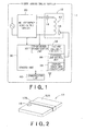
- FIG. 1 illustrates a schematic configuration of a power transmitting apparatus according to the present exemplary embodiment.
- a power transmitting apparatus 1 includes a resonator 10, a high-frequency power supply circuit 20, a control unit 30, and a communication unit 40.
- the power transmitting apparatus 1 transmits electric power to a power receiving apparatus, by mutual coupling between the resonator 10 and a resonator of the power receiving apparatus (not illustrated).
- the power transmitting apparatus 1 may include a temperature sensor configured to monitor heating of the power transmitting apparatus 1, a sensor configured to monitor a foreign object by electromagnetic wave radar and ultrasonic wave radar, and a sensor such as an RFID for detecting the position of the resonator of the power receiving apparatus.
- the resonator 10 has a coil 12, a capacitor 14, and a parasitic loop element 16.
- the capacitor 14 may be a parasitic capacitor.
- the parasitic loop element 16 will be described below.
- the high-frequency power supply circuit 20 supplies AC power to the resonator 10.
- the AC power may be supplied via a wiring or may be supplied wirelessly.
- the communication unit 40 can communicate with a communication unit (not illustrated) of the power receiving apparatus, and receives the power receiving status and the amount of required power of the power receiving apparatus, or transmits the power transmitting status of the power transmitting apparatus 1.
- the control unit 30 has a transmission power monitor unit 32, a resonant frequency monitor unit 34, a parasitic loop control unit 36, and a coupling coefficient monitor unit 38.
- the transmission power monitor unit 32 has an ammeter, a voltmeter or the like for detecting the power transmission current, voltage, and electric power.
- the control unit 30 controls the output of the high-frequency power supply circuit 20 based on the power transmitting current, the voltage, and the electric power detected by the transmission power monitor unit 32, or the power receiving current, the voltage, and the electric power of the power receiving apparatus received via the communication unit 40.
- the resonant frequency monitor unit 34 determines whether or not the resonator 10 is in the resonant condition. For example, in a series resonant circuit in which a capacitor and a coil are connected in series, the impedance is minimized at the resonant frequency, and the current is maximized. For that reason, by sweeping the output frequency of the high-frequency power supply circuit 20, the frequency at which a current value of an input end of the resonator 10 is maximized can be determined as the resonant frequency. The resonant frequency monitor unit 34 determines whether or not the resonator 10 is in the resonant condition based on the change in the current value of the input end of the resonator 10.
- the parasitic loop control unit 36 controls the parasitic loop element 16 so that the resonant frequency (resonant condition) of the resonator 10, the inductance value, or an LC product becomes a desired value based on the monitoring results of the transmission power monitor unit 32, the resonant frequency monitor unit 34, and the coupling coefficient monitor unit 38, and the power receiving status of the power receiving apparatus received via the communication unit 40.
- the control of the parasitic loop element 16 will be described below.
- FIG. 2 is a perspective view of the coil 12 and the parasitic loop element 16 included in the resonator 10.
- the coil 12 includes a magnetic core 12A, and a winding portion 12B that is wound around the magnetic core 12A.
- the magnetic core 12A for example, ferrite can be used.
- the winding portion 12B and the parasitic loop element 16 for example, a copper wire can be used.
- the parasitic loop element 16 is a parasitic element formed in a loop shape arranged near the coil 12 and on a surface of the magnetic core 12A.
- the parasitic loop element 16 is arranged in a peripheral portion of the magnetic core 12A and in the vicinity of the winding portion 12B.
- the parasitic loop element 16 includes a switch, not illustrated, when the switch is turned on, a loop is formed, and when the switch is turned off, the loop is opened. That is, the loop is opened and closed by turning on/off the switch.
- the parasitic loop control unit 36 controls turning on-off of the switch.
- the switch may be a mechanical switch, or may be an electrical switch such as a semiconductor switch.
- the power receiving apparatus includes a power receiving side resonator configured to receive the electric power by mutual inductance between the power receiving apparatus and the resonator 10 of the power transmitting apparatus 1, a rectifier configured to convert AC power received via the power receiving side resonator into DC power, a buck-boost circuit configured to raise and/or lower the voltage based on the operating voltage of the load, a control unit configured to control each portion of the power receiving apparatus, and a communication unit.
- the communication unit can communicate with the communication unit 40 of the power transmitting apparatus 1, and transmits the power receiving status of the power receiving apparatus or receives the power transmitting status of the power transmitting apparatus 1.
- the power receiving side coil receives AC power from the power transmitting side coil 12 through the coupling with mutual coupling.
- the power receiving side resonator may supply AC power to the rectifier via the wiring, and may supply AC power wirelessly.
- the AC power from the power receiving side resonator may be connected to the rectifier after being boosted and bucked in the buck-boost circuit, and may be boosted and bucked in a DC/DC converter after being converted to DC power by the rectifier.
- the load supplied with the DC power from the rectifier or the buck-boost circuit is a load circuit or a battery, and immediately consumes or charges the supplied DC power.
- FIG. 3 illustrates an equivalent circuit of the coil 12 on which the parasitic loop element 16 is arranged.
- a self-inductance value of the coil 12 is assumed to be L 1
- a self-inductance value of the parasitic loop element 16 is assumed to be L L
- a mutual inductance generated by magnetically coupling the coil 12 and the parasitic loop element 16 is assumed to be M.
- an impedance Z of the coil 12 is expressed by the following Formula 2.
- Z j ⁇ ⁇ ⁇ L 1 - k 2 ⁇ L L
- the self-inductance value of the coil 12 in consideration of the parasitic loop element 16 is expressed in the following Formula 5.
- the current I L flowing through the parasitic loop element 16 is M/L L times the current I 1 flowing through the coil 12. Therefore, when L L increases, it is possible to reduce the current flowing through the parasitic loop element 16. For example, when the number of winding of the parasitic loop element 16 is assumed to be an N winding, as compared with the case of one winding, the flowing current can be reduced to 1/N.
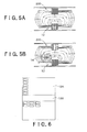
- FIG. 5A is an example of the magnetic field distribution when there is no parasitic loop element 16, that is, when the loop is opened by turning off the switch.
- FIG. 5B is an example of the magnetic field distribution when there is the parasitic loop element 16, that is, when that loop is closed by turning on the switch.
- the parasitic loop element 16 is illustrated above the coil 12 in FIG. 5B .
- the leak inductance value (self-inductance value) of the coil 12 decreases.
- the loop of the parasitic loop element 16 is kept open by turning off the switch. Moreover, when the coil 12 and the power receiving side coil 200 approach to each other or are displaced in each other, the inductance value increases, and the resonant frequency is varied, the loop of the parasitic loop element 16 is closed by turning on the switch. Accordingly, it is possible to reduce the self-inductance value of the coil 12, and maintain the resonant condition.
- the parasitic loop control unit 36 may perform the opening and closing control of the parasitic loop element 16 based on the deviation (a change in resonant condition) of the resonant frequency monitored by the resonant frequency monitor unit 34, and the parasitic loop control unit 36 may perform the opening and closing control of the parasitic loop element 16 by separately preparing tables of the coupling coefficient and the inductance value, and detecting the fluctuation of the inductance value from the monitoring result of the coupling coefficient monitor unit 38.
- the opening and closing of the parasitic loop element 16 by switching the opening and closing of the parasitic loop element 16 to adjust an amount of flux linkage of the parasitic loop element 16, it is possible to vary the self-inductance value of the coil 12. Accordingly, when the resonant frequency (resonant condition) fluctuates by distance between the transmitting and receiving coils or the misalignment therebetween, it is possible to keep the resonant condition by changing the inductance value of the coil 12, thereby suppressing the degradation of transmission efficiency.
- the amount of flux linkage may be adjusted by providing the parasitic loop element 16 so as to be movable on the surface of the magnetic core 12A and by changing the position of the parasitic loop element 16. For example, when the parasitic loop element 16 is arranged at positions P1 to P6 illustrated in FIG. 6 , an amount of variation of the inductance value is as illustrated in FIG. 7 .
- the parasitic loop element 16 is set to be movable at positions P1, P2, and P3. That is, the parasitic loop element 16 is set to be movable between a central portion of the magnetic core 12A and the peripheral portion (side portion) along the winding portion 12B.
- the parasitic loop control unit 36 is able to maintain the resonant condition by changing the position of the parasitic loop element 16 based on the deviation of the resonant frequency or the like to vary the inductance value.
- the parasitic loop element 16 may be set to be movable at the positions P4, P5, and P6. That is, the parasitic loop element 16 may be set to be movable between the central portion and the corner of the magnetic core 12A along the peripheral portion of the magnetic core 12A.
- a plurality of the parasitic loop elements 16 including a switch for switching the opening and closing of the loop may be provided on the surface of the magnetic core 12A such that the parasitic loop control unit 36 may control the opening and closing of each of the parasitic loop elements 16.
- the plurality of the parasitic loop elements 16 may have the same size, or may have different sizes. By increasing the size of the parasitic loop element 16, it is possible to increase the amount of change in inductance value.
- the parasitic loop element 16 may be arranged on the surface of the magnetic core 12A in the vicinity of the winding portion 12B to be perpendicular to the surface of the magnetic core 12A, and the parasitic loop element 16 may be rotated around the perpendicular line to the surface of the magnetic core 12A.
- the amount of flux linkage changes by the rotation angle of the parasitic loop element 16, and the resonant condition can be maintained by changing the inductance value.
- the rotation of the parasitic loop element 16 may be performed, for example, by the use of a motor, not illustrated.
- the parasitic loop element 16 may be arranged obliquely with respect to the surface of the magnetic core 12A, and an inclination angle (an angle formed between the parasitic loop element 16 and the surface of the magnetic core 12A) of the parasitic loop element 16 may be changed.
- the amount of flux linkage changes by the inclination angle of the parasitic loop element 16, and the resonant condition can be maintained by changing the inductance value.
- the inclination angle of the parasitic loop element 16 may be adjusted, for example, by the use of a motor (not illustrated).
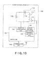
- a parasitic loop element 116 may be provided in a resonator 110 of a power receiving apparatus 100.
- the power receiving apparatus 100 includes the resonator 110, a load 120, a control unit 130, and a communication unit 140. Power is transmitted to the power receiving apparatus 100 from the power transmitting apparatus 1 by mutual coupling between resonator 110 and the resonator 10 (refer to FIG. 1 ) of the power transmitting apparatus 1.
- the resonator 110 has a coil 112, a capacitor 114, and the parasitic loop element 116.
- the capacitor 114 may be a parasitic capacitor.
- the load 120 is supplied with the power from the resonator 110.
- the communication unit 140 is able to communicate with the communication unit 40 (refer to FIG. 1 ) of the power transmitting apparatus 1, and receives the transmitting status of the power transmitting apparatus 1 or transmits the receiving status of the power receiving apparatus 100 or the required amount of power.
- the control unit 130 has a power receiving monitor unit 132, a resonant frequency monitor unit 134, and a parasitic loop control unit 136.
- the power receiving monitor unit 132 has a voltmeter, an ammeter or the like for detecting the receiving current, the voltage, and the power.
- the resonant frequency monitor unit 134 determines whether or not the resonator 110 is in the resonant condition based on the change in the current value of the output end of the resonator 110.
- the parasitic loop control unit 136 controls the parasitic loop element 116 based on the monitoring results of the power receiving monitor unit 132 and the resonant frequency monitor unit 134, and the power transmitting status of the power transmitting apparatus 1 received via the communication unit 140 so that the resonant frequency (resonant condition) of the resonator 110, the inductance value, or the LC product is a desired value.
- a method of controlling the parasitic loop element 116 is similar to the method of controlling the parasitic loop element 16 described above.
- a fixed parasitic loop element without opening and closing the loop may be arranged in the vicinity of the magnetic core.
Applications Claiming Priority (1)
| Application Number | Priority Date | Filing Date | Title |
|---|---|---|---|
| JP2013044387A JP6071655B2 (ja) | 2013-03-06 | 2013-03-06 | 無線電力伝送装置 |
Publications (2)
| Publication Number | Publication Date |
|---|---|
| EP2775583A2 true EP2775583A2 (de) | 2014-09-10 |
| EP2775583A3 EP2775583A3 (de) | 2014-11-19 |
Family
ID=50071530
Family Applications (1)
| Application Number | Title | Priority Date | Filing Date |
|---|---|---|---|
| EP14154829.7A Withdrawn EP2775583A3 (de) | 2013-03-06 | 2014-02-12 | Resonator und drahtlose Leistungsübertragungsvorrichtung |
Country Status (4)
| Country | Link |
|---|---|
| US (1) | US20140252868A1 (de) |
| EP (1) | EP2775583A3 (de) |
| JP (1) | JP6071655B2 (de) |
| CN (1) | CN104037950A (de) |
Families Citing this family (15)
| Publication number | Priority date | Publication date | Assignee | Title |
|---|---|---|---|---|
| JP6071654B2 (ja) | 2013-03-06 | 2017-02-01 | 株式会社東芝 | コイル、受電装置、及び送電装置 |
| JP2014204603A (ja) * | 2013-04-08 | 2014-10-27 | ソニー株式会社 | 給電装置および給電システム |
| JP6315382B2 (ja) * | 2013-12-19 | 2018-04-25 | パナソニックIpマネジメント株式会社 | 無線電力伝送のための送電装置および受電装置ならびに無線電力伝送システム |
| US10170939B2 (en) * | 2014-02-28 | 2019-01-01 | Panasonic Intellectual Property Management Co. Ltd. | Foreign object detector, power transmitting device and power receiving device for wireless power transmission, and wireless power transmission system |
| US10224753B2 (en) | 2015-05-27 | 2019-03-05 | Qualcomm Incorporated | Wireless power transfer using a field altering circuit |
| JP6287993B2 (ja) * | 2015-08-04 | 2018-03-07 | トヨタ自動車株式会社 | 車両 |
| JP6988643B2 (ja) * | 2018-03-29 | 2022-01-05 | Tdk株式会社 | ワイヤレス受電装置、及びワイヤレス電力伝送システム |
| US10505394B2 (en) * | 2018-04-21 | 2019-12-10 | Tectus Corporation | Power generation necklaces that mitigate energy absorption in the human body |
| US10895762B2 (en) | 2018-04-30 | 2021-01-19 | Tectus Corporation | Multi-coil field generation in an electronic contact lens system |
| US10838239B2 (en) | 2018-04-30 | 2020-11-17 | Tectus Corporation | Multi-coil field generation in an electronic contact lens system |
| US10790700B2 (en) | 2018-05-18 | 2020-09-29 | Tectus Corporation | Power generation necklaces with field shaping systems |
| US11137622B2 (en) | 2018-07-15 | 2021-10-05 | Tectus Corporation | Eye-mounted displays including embedded conductive coils |
| US10838232B2 (en) | 2018-11-26 | 2020-11-17 | Tectus Corporation | Eye-mounted displays including embedded solenoids |
| US10644543B1 (en) | 2018-12-20 | 2020-05-05 | Tectus Corporation | Eye-mounted display system including a head wearable object |
| US10944290B2 (en) | 2019-08-02 | 2021-03-09 | Tectus Corporation | Headgear providing inductive coupling to a contact lens |
Family Cites Families (11)
| Publication number | Priority date | Publication date | Assignee | Title |
|---|---|---|---|---|
| JPH08162331A (ja) * | 1994-12-05 | 1996-06-21 | Hitachi Ltd | 可変インダクタ及びそれを用いた半導体集積回路 |
| JPH1140428A (ja) * | 1997-07-23 | 1999-02-12 | Hokko Denshi Kk | うず電流を利用した可変コイル |
| US6549096B2 (en) * | 2001-03-19 | 2003-04-15 | International Business Machines Corporation | Switched inductor/varactor tuning circuit having a variable integrated inductor |
| JP2006148518A (ja) * | 2004-11-19 | 2006-06-08 | Matsushita Electric Works Ltd | 非接触icカードの調整装置および調整方法 |
| JP4468297B2 (ja) * | 2005-12-28 | 2010-05-26 | 株式会社東芝 | 可変インダクタ素子およびその製造方法、移動無線装置 |
| JP4911148B2 (ja) * | 2008-09-02 | 2012-04-04 | ソニー株式会社 | 非接触給電装置 |
| US20120256494A1 (en) * | 2008-09-27 | 2012-10-11 | Kesler Morris P | Tunable wireless energy transfer for medical applications |
| JP5240786B2 (ja) * | 2009-08-25 | 2013-07-17 | 国立大学法人埼玉大学 | 非接触給電装置 |
| US8934857B2 (en) * | 2010-05-14 | 2015-01-13 | Qualcomm Incorporated | Controlling field distribution of a wireless power transmitter |
| JP5404573B2 (ja) * | 2010-09-27 | 2014-02-05 | 株式会社東芝 | 無線電力伝送装置および無線電力受信装置 |
| EP2632762B1 (de) * | 2010-10-29 | 2017-05-31 | Qualcomm Incorporated(1/3) | Drahtlose energieübertragung über gekoppelte parasitäre resonatoren |
-
2013
- 2013-03-06 JP JP2013044387A patent/JP6071655B2/ja active Active
-
2014
- 2014-02-12 EP EP14154829.7A patent/EP2775583A3/de not_active Withdrawn
- 2014-02-20 US US14/185,035 patent/US20140252868A1/en not_active Abandoned
- 2014-03-05 CN CN201410077790.3A patent/CN104037950A/zh active Pending
Non-Patent Citations (1)
| Title |
|---|
| None |
Also Published As
| Publication number | Publication date |
|---|---|
| JP6071655B2 (ja) | 2017-02-01 |
| CN104037950A (zh) | 2014-09-10 |
| EP2775583A3 (de) | 2014-11-19 |
| JP2014176139A (ja) | 2014-09-22 |
| US20140252868A1 (en) | 2014-09-11 |
Similar Documents
| Publication | Publication Date | Title |
|---|---|---|
| EP2775583A2 (de) | Resonator und drahtlose Leistungsübertragungsvorrichtung | |
| US10493856B2 (en) | System, apparatus and method for optimizing wireless charging alignment | |
| JP6092017B2 (ja) | 送電装置、非接触給電システム、及び制御方法 | |
| US10250079B2 (en) | Method and apparatus for wirelessly transmitting power and power transmission information | |
| KR102014126B1 (ko) | 무선 전력 수신기 시스템 | |
| US9984814B2 (en) | Wireless power transmitter, wireless power relay apparatus, and wireless power receiver | |
| US9680336B2 (en) | Wireless power repeater and method thereof | |
| EP2949024B1 (de) | Vorrichtung zur drahtlosen stromübertragung und verfahren zur drahtlosen stromübertragung damit | |
| KR101783727B1 (ko) | 수전 장치, 급전 시스템 | |
| US20140265615A1 (en) | Method and apparatus for controlling wireless power transmission | |
| US20130069753A1 (en) | High frequency pcb coils | |
| US20130207603A1 (en) | Wireless energy transmission | |
| JP6305517B2 (ja) | 共振型電力伝送装置 | |
| JP6089464B2 (ja) | 非接触電力伝送装置 | |
| US20240079909A1 (en) | Systems and Methods for Dynamically Tuning a Wireless Power Transfer System | |
| US10651657B2 (en) | Dynamic adjustment of power for wireless power transmission | |
| EP2427957B1 (de) | Elektromagnetische Vorrichtung mit geteiltem Fluss in einer magnetischen Parallelschaltung mit mehreren Verbrauchern und Betriebsverfahren dafür | |
| JP6858151B2 (ja) | 無線給電装置及びそのインピーダンス調整方法 | |
| Usikalu et al. | Investigation into wireless power transfer in near field using induction technique | |
| Hua et al. | Extending the inductive power transfer range by using passive power repeaters |
Legal Events
| Date | Code | Title | Description |
|---|---|---|---|
| PUAI | Public reference made under article 153(3) epc to a published international application that has entered the european phase |
Free format text: ORIGINAL CODE: 0009012 |
|
| 17P | Request for examination filed |
Effective date: 20140212 |
|
| AK | Designated contracting states |
Kind code of ref document: A2 Designated state(s): AL AT BE BG CH CY CZ DE DK EE ES FI FR GB GR HR HU IE IS IT LI LT LU LV MC MK MT NL NO PL PT RO RS SE SI SK SM TR |
|
| AX | Request for extension of the european patent |
Extension state: BA ME |
|
| PUAL | Search report despatched |
Free format text: ORIGINAL CODE: 0009013 |
|
| AK | Designated contracting states |
Kind code of ref document: A3 Designated state(s): AL AT BE BG CH CY CZ DE DK EE ES FI FR GB GR HR HU IE IS IT LI LT LU LV MC MK MT NL NO PL PT RO RS SE SI SK SM TR |
|
| AX | Request for extension of the european patent |
Extension state: BA ME |
|
| RIC1 | Information provided on ipc code assigned before grant |
Ipc: H02J 5/00 20060101AFI20141016BHEP Ipc: H04B 5/00 20060101ALI20141016BHEP |
|
| STAA | Information on the status of an ep patent application or granted ep patent |
Free format text: STATUS: EXAMINATION IS IN PROGRESS |
|
| 17Q | First examination report despatched |
Effective date: 20171031 |
|
| STAA | Information on the status of an ep patent application or granted ep patent |
Free format text: STATUS: THE APPLICATION IS DEEMED TO BE WITHDRAWN |
|
| 18D | Application deemed to be withdrawn |
Effective date: 20180512 |