EP2753964B1 - Hermetic small form factor optical device packaging for plastic optical fiber networks - Google Patents
Hermetic small form factor optical device packaging for plastic optical fiber networks Download PDFInfo
- Publication number
- EP2753964B1 EP2753964B1 EP12759291.3A EP12759291A EP2753964B1 EP 2753964 B1 EP2753964 B1 EP 2753964B1 EP 12759291 A EP12759291 A EP 12759291A EP 2753964 B1 EP2753964 B1 EP 2753964B1
- Authority
- EP
- European Patent Office
- Prior art keywords
- optical fiber
- section
- enclosure
- fiber lead
- pcs
- Prior art date
- Legal status (The legal status is an assumption and is not a legal conclusion. Google has not performed a legal analysis and makes no representation as to the accuracy of the status listed.)
- Active
Links
Images


Classifications
-
- G—PHYSICS
- G02—OPTICS
- G02B—OPTICAL ELEMENTS, SYSTEMS OR APPARATUS
- G02B6/00—Light guides; Structural details of arrangements comprising light guides and other optical elements, e.g. couplings
- G02B6/24—Coupling light guides
- G02B6/42—Coupling light guides with opto-electronic elements
- G02B6/4201—Packages, e.g. shape, construction, internal or external details
- G02B6/4248—Feed-through connections for the hermetical passage of fibres through a package wall
-
- G—PHYSICS
- G02—OPTICS
- G02B—OPTICAL ELEMENTS, SYSTEMS OR APPARATUS
- G02B6/00—Light guides; Structural details of arrangements comprising light guides and other optical elements, e.g. couplings
- G02B6/24—Coupling light guides
- G02B6/42—Coupling light guides with opto-electronic elements
- G02B6/4201—Packages, e.g. shape, construction, internal or external details
- G02B6/4251—Sealed packages
-
- G—PHYSICS
- G02—OPTICS
- G02B—OPTICAL ELEMENTS, SYSTEMS OR APPARATUS
- G02B6/00—Light guides; Structural details of arrangements comprising light guides and other optical elements, e.g. couplings
- G02B6/02—Optical fibres with cladding with or without a coating
- G02B6/02033—Core or cladding made from organic material, e.g. polymeric material
Definitions
- the present disclosure is generally related to hermetically-sealed optical components for plastic optical fiber networks used in harsh aerospace environment.
- Optical networking using plastic optical fibers may provide advantages over networking using copper or other metal wiring.
- Plastic optical fiber networking may have lower installation and maintenance costs.
- using plastic optical fibers may result in appreciable weight savings.
- the weight savings may be significant for networks aboard vehicles, such as aircraft, where the weight savings may result in reduced fuel consumption and lower emissions.
- Document EP 0 872 748 A2 shows conventional optical fiber not coated with a metal layer.
- a solder layer is filled into between a case, for an optical module wherein an optical element is optically coupled with the optical fiber within the case, and a cover conforming to the shape of the case, thereby simply conducting hermetical sealing.
- a resin such as a silicone resin, is potted in the optical fiber introducing section.
- the two-layer hermetical sealing can realize a method for hermetically sealing an optical fiber introducing section which can maintain airtightness high enough to ensure long-term reliability of an optical module. This can facilitate the hermetical sealing of an optical device particularly in its optical fiber introducing section.
- Document US 2004/0114884 A1 shows an optical-electronic package for an electronic device providing electrical connections to the electronic device and optical fiber connections to the electronic device.
- the package includes a high thermal conductivity base which has a pedestal to support and provide heat transfer connection to the electronic device.
- a seal band is formed on the base and a casing is bonded to the seal band.
- the casing has side feedthroughs for the electrical connections from the electronic device, and the casing has top feedthroughs or grooves for the optical fiber connections from the electronic device.
- a lid is hermetically sealed to the top of the casing.
- the lid has retractable means for forming a bend in the optical fibers to provide strain relief when the lid is placed on the casing.
- the retractable means for forming a bend in the optical fibers is retractable once the lid is sealed on the casing.
- Document EP 1 596 233 A1 shows an optical module, wherein an optical fiber and an optical semi-conductor element are connected optically.
- optical devices such as transmitters, receivers, and transceivers may be hermetically sealed.
- optical devices may be deployed in locations on the exterior of the aircraft, such as near engines or near the landing gear, that may not be pressurized or insulated against the ambient environment. If the optical devices in such locations are not hermetically sealed, condensation, particulates, and other undesired material may form on the optical devices or on exposed ends of the plastic optical fibers.
- Conventional methods of hermetic sealing optical devices may involve many precise manufacturing steps that are expensive. In addition, certain steps of conventional methods may use processing temperatures that can damage plastic optical fiber.
- an optical device including one or more optoelectronic devices within an enclosure
- the optical fiber leads may include a portion or length of a polymer-clad silica fiber, such as HCS® fiber, which is a registered trademark of FURUKAWA ELECTRIC NORTH AMERICA, INC.
- Hermetically sealing the optical device to the one or more optical fiber leads enables use of the hermetically sealed optical component in potentially harsh environments. Production of the hermetically sealed optical components involves relatively few steps, thus, enabling the hermetically sealed optical components to be produced at relatively low cost.
- a particular enclosure for a hermetically sealed optical component may include a first section that includes a base portion and wall portions to receive an optoelectronic device.
- the first section includes an open-ended slot in one of the wall portions through which a polymer-clad silica (PCS) optical fiber lead may be received.
- the PCS optical fiber lead may be guided in place adjacent the optoelectronic device housed in the first section by an alignment body.
- the PCS optical fiber lead may have a metalized section at a point where the PCS optical fiber lead is received into the open-ended slot in the wall portion of the first section.
- the PCS optical fiber lead may be aligned to the optoelectronic device and may be mechanically coupled to the first section, such as by epoxy, to secure the PCS optical fiber lead to the first section outside the wall portion of the first section.
- a second section of the enclosure is installed over the first section.
- the second section may be shaped to engage edges of the wall portion of the first section.
- the second section may include or be coupled to a layer of solder to join the second section to the edges of the wall section and to the metalized portion of the PCS optical fiber lead. Heat may be applied to the second section adjacent to locations where the second section meets the edges of the first section to melt the solder.
- the second section may be joined to the first section and the PCS optical fiber lead may be soldered in place and sealed to the first section and to the second section of the enclosure.
- the enclosure housing the optoelectronic device and the PCS optical fiber leads together from an optical component that can be coupled to a plastic optical fiber with low insertion loss.
- an apparatus in a particular embodiment, includes an enclosure configured to contain at least one optoelectronic device and to interface the at least one optoelectronic device to a PCS optical fiber lead.
- the enclosure includes a first section that includes a base portion and a wall portion.
- the wall portion is coupled to a perimeter about the base portion.
- the wall portion defines an open-ended slot in a first edge, which includes an open end that is configured to receive a first portion of the PCS optical fiber lead extending through the wall portion.
- a second section is configured to sealingly engage the first edge of the wall portion and the first portion of the PCS optical fiber lead at the open end of the open-ended slot.
- a method in another particular embodiment, includes, at a first section of an enclosure having a base portion and a wall portion coupled to a perimeter of the base portion, receiving a first portion of a PCS optical fiber lead at an open end of an open-ended slot in a first edge of the wall portion.
- the first portion of the PCS optical fiber lead is received such that an end of the PCS optical fiber lead is aligned with an optical surface of an optoelectronic device and the first portion of the PCS optical fiber lead extends through the wall portion.
- the PCS optical fiber lead is physically secured to the first portion of the enclosure outside the wall portion.
- the enclosure is hermetically sealed by fixably joining a second section of the enclosure to the first edge of the wall portion and to the first portion of the PCS optical fiber lead.
- an enclosure in still another particular embodiment, includes a first section that includes a base portion and a wall portion.
- the wall portion is coupled to a perimeter about the base portion.
- the wall portion includes a first open-ended slot configured to receive a first metalized portion of a first PCS optical fiber lead extending through the wall portion.
- the enclosure also includes a second section.
- the second section includes a second edge with a preformed solder layer to fixably engage the first edge of the wall portion and the first metalized portion of the first PCS optical fiber lead at the open-ended slot when heat is applied adjacent to the second edge.
- an apparatus which includes an enclosure configured to contain at least one optoelectronic device and to interface the at least one optoelectronic device to a polymer-clad silica (PCS) optical fiber.
- the enclosure includes a first section including a base portion and a wall portion coupled to a perimeter about the base portion.
- the wall portion defines an open-ended slot in a first edge and the open-ended slot includes an open end that is configured to receive a first portion of a PCS optical fiber lead extending through the wall portion.
- a second section is configured to sealingly engage the first edge of the wall portion and the first portion of the optical fiber lead at the open end of the open-ended slot.
- the first portion of the PCS optical fiber lead includes a metalized outer region.
- the second section may include a cap portion surrounded by a second wall portion extending to a second edge.
- the second edge is configured to sealingly engage the first edge of the wall portion and the first portion of the PCS optical fiber lead.
- the cap portion may include a concave surface and the concave surface is configured to accommodate the at least one optoelectronic device.
- the present invention may further comprise a preformed solder layer of the second edge and heat applied proximate to the second edge causes the preformed solder layer to flow to seal the second edge to the first edge of the first section and to the first portion of the PCS optical fiber lead.
- the first section includes a first cable support member extending from the wall portion adjacent to the open-ended slot, wherein the first cable support member is configured to engage the PCS optical fiber lead outside the wall portion.
- the second section includes a second cable support member, wherein the second cable support member is configured to engage the PCS optical fiber lead.
- the present invention may further comprise an adhesive coupling the PCS optical fiber lead to the first cable support member and to the second cable support member.
- the present invention may further comprise a boot configured to be slidably positioned over the first cable support member and the second cable support member.
- the present invention may further comprise an alignment body coupled to the base portion and configured to guide alignment of the PCS optical fiber lead to an optical surface of the at least one optoelectronic device.
- the present invention may further comprise a plurality of conductive pins extending through the base portion, wherein the base portion is sealingly engaged with the plurality of conductive pins.
- a method which includes, at a first section of an enclosure having a base portion and a wall portion coupled to a perimeter of the base portion, receiving a first portion of a polymer-clad silica (PCS) optical fiber lead at an open end of an open-ended slot in a first edge of the wall portion such that an end of the PCS optical fiber lead is aligned with an optical surface of an optoelectronic device and the first portion of the PCS optical fiber lead extends through the wall portion, physically securing the PCS optical fiber lead to the first portion of the enclosure outside the wall portion, and hermetically sealing the enclosure by fixably joining a second section of the enclosure to the first edge of the wall portion and to the first portion of the PCS optical fiber lead.
- PCS polymer-clad silica
- the first portion of the PCS optical fiber lead may include a metalized outer region and wherein fixably joining the second section of the enclosure to the first edge of the wall portion and to the first portion of the PCS optical fiber lead includes soldering the second section to the first edge and to the metalized outer region of the first portion of the PCS optical fiber lead.
- the present invention may further include positioning a preformed solder layer along the second section and applying heat adjacent to the second section using heated rollers
- a silica core of the PCS optical fiber lead may extend through the wall portion of the first section and an outer jacket of the PCS optical fiber lead is physically secured to the enclosure outside the wall portion.
- the present invention may further include physically securing the first portion of the PCS optical fiber lead to a second cable support member extending from the second section of the enclosure.
- the present invention may further include coupling a boot over the first cable support member, the second cable support member, and the first portion of the PCS optical fiber lead.
- an enclosure including a first section which includes a base portion and a wall portion coupled to the base portion.
- the wall portion includes a first open-ended slot configured to receive a metalized portion of a polymer-clad silica (PCS) optical fiber lead that extends through the wall portion.
- the enclosure also includes a second section which includes a second edge configured to support a preformed solder layer to sealingly engage a first edge of the wall portion and the metalized portion of the PCS optical fiber lead when heat is applied adjacent to the second edge.
- PCS polymer-clad silica
- the present invention may further include an alignment block attached to at least one of the base portion and the wall portion using a metal-to-ceramic brazing.
- the alignment block may be configured to receive an optoelectronic device and a portion of the PCS optical fiber such that an optical surface of the optoelectronic device and an end for the PCS optical fiber lead are aligned.
- the optoelectronic device may have a TO18 type packaging.
- the optoelectronic device may have a ceramic or metal submount type packaging.
- the alignment block may be formed using a ceramic molding process.
- the hermetically sealed optical components may house one or more optoelectronic devices and may be adapted to be coupled to optical fibers as part of an optical fiber network.
- the hermetically sealed optical components may be formed using low-cost, high volume manufacturing processes.
- the hermetically sealed optical components may be particularly well suited for coupling to plastic optical fibers with relatively low insertion losses.
- an enclosure in a particular embodiment, includes a first section that includes a base portion and wall portions to receive one or more optoelectronic devices.
- the first section includes one or more open-ended slots in one of the wall portions through which one or more optical fiber leads may be received.
- An optical fiber lead may be guided into alignment with an optoelectronic device housed in the first section by a high precision alignment body (e.g., a precision molded ceramic block).
- the optical fiber lead may have a metalized region at a point where the optical fiber lead is received into an open-ended slot in the wall portion of the first section.
- a portion of the optical fiber lead may be physically coupled to the first section, such as by epoxy or another adhesive, to secure the optical fiber lead to the first section outside the wall portion.
- the optical fiber lead may include a silica core and a hard polymer cladding.
- the optical fiber lead may include a portion or length of polymer-clad silica (PCS) fiber.
- PCS polymer-clad silica
- the optical fiber lead may be adapted to couple to a plastic optical fiber with relatively low insertion loses.
- the optical fiber lead may have an outer diameter and numerical aperture that is substantially equal to a standard poly(methyl methacrylate) (PMMA) plastic optical fiber.
- a second section of the enclosure may be installed over the first section.
- the second section may be shaped to engage edges of the wall portion of the first section.
- the second section may include or be coupled to a layer of solder to join the second section to the edges of the wall section and to the metalized portion of the optical fiber lead.
- the metalized portion may be a metalized outer region. Heat may be applied to the second section adjacent to locations where the second section meets the edges of the first section to melt the solder.
- the second section may be sealed to the first section and the optical fiber lead to form a hermetically sealed optical component.
- FIG. 1 is a side cross-sectional view of a particular embodiment of an enclosure 100 having a first section 110 and a second section 160 configured to receive one or more optoelectronic devices (not shown in FIG. 1 ) and to hermetically seal the one or more optoelectronic devices at an end of an optical fiber lead (also not shown in FIG. 1 ).
- the first section includes a base portion 120.
- a plurality of conductive pins 124 extend through the base portion 120 to enable the optoelectronic devices within the first section 110 to be electrically coupled to other devices outside the enclosure 100.
- the conductive pins 124 are hermetically sealed to the base portion 120.
- the base portion 120 may be molded around the conductive pins 124 so that the surfaces of the conductive pins 124 are integral with the base portion 120.
- the enclosure 100 and the conductive pins 124 may be arrange to conform to the Multi-Source Agreement (MSA) Small Form-Factor (SFF) specification.
- MSA Multi-Source Agreement
- SFF Small Form-Factor
- the conductive pins 124 may be arranged in a 2x5 dual-in-line configuration.
- the enclosure 100 may have physical dimensions that conform to the MSA SFF specification.
- the enclosure 100 may also include alignments posts 128 as prescribed by the MSA SFF specification.
- the base portion 120 may be joined with a first wall portion 130 that extends about a perimeter 122 of the base portion 120.
- the first wall portion 130 of the enclosure 100 includes a first edge 140 that extends around the periphery of the first wall portion 130.
- the first edge 140 of the first wall portion 130 is configured to be sealed to a second edge 180 of the second section 160, as further described below.
- the first wall portion 130 includes a first wall 132 at one end of the base portion 120 and a second wall 134 at an opposite end of the base portion 120.
- the first wall 132 includes an open-ended slot 142 formed in the first edge 140.
- the open-ended slot 142 includes an open end 144 that is configured to receive an end of an optical fiber lead (not shown in FIG. 1 ).
- the optical fiber lead may be received into the open-ended slot 142, in the frame of reference of FIG. 1 , by lowering the optical fiber lead through the open end 144 of the open-ended slot 142 until the optical fiber lead rests within the open ended slot 142.
- the first wall 132 may also include or be coupled to a first cable support member 150 that extends outwardly from the first wall 132.
- the optical fiber lead may be physically coupled to the first cable support member 150, such as by an adhesive, to hold the optical fiber lead in place while the enclosure 100 is hermetically sealed.
- the first section 110 of the enclosure 100 also may include or be coupled to a high precision alignment body 156.
- the high precision alignment body 156 may include a precision molded ceramic element that is coupled to one or both of the base portion 120 and the first wall portion 132.
- the alignment body 156 includes one or more grooves 158 and 159, e.g., one groove for each optical fiber lead that is to be received by the enclosure 100.
- Each of the grooves 158 or 159 may be configured to align an end of an optical fiber lead with an optoelectronic device (not shown in FIG. 1 ) within the enclosure 100 such that the optical fiber leads and optoelectronic devices are properly aligned after the enclosure 100 is hermetically sealed.
- precision molding of the alignment body 156 enables the optoelectronic devices and optical fiber leads to be aligned passively (e.g., by the accurate physical placement of the components inside 110) and no active alignment is needed.
- active alignment refers to passing light through an optical fiber lead and moving the optical fiber lead to test whether the optical fiber lead is properly aligned with an optoelectronic device.
- the second section 160 of the enclosure 100 includes a cap portion 170 surrounded by a second wall portion 172.
- the cap portion 170 may have a concave inner surface in order to accommodate devices within the enclosure 100 (e.g. one or more optoelectronic devices and interface circuitry 126).
- the second wall portion 172 extends to the second edge 180, which is configured to sealingly engage the first edge 140 of the first section 110 and the optical fiber leads, as further described with reference to FIG. 5 .
- the second edge 180 may include or be coupled to a preformed solder layer 190 that fully extends around a perimeter of the second edge 180.
- the preformed solder layer 190 is configured so that, when heat is applied to the second section 160 adjacent to the second edge 180, the preformed solder layer 190 melts to sealingly engage the second edge 180 of the second section 160 with the first edge 140 of the first section 110 and the optical fiber leads, as further described with reference to FIG. 5 .
- a second cable support member 1 66 may extend from the second edge 180 of the second section 160 opposite the first cable support member 150 of the first section 110 of the enclosure 100 to support one or more optical fiber leads (not shown in FIG. 1 ).
- FIG. 2 is a top view of the first section 110 of the enclosure 100 of FIG. 1 .
- the base portion 120 supports the conductive pins 124 that permit electrical connection of optoelectronic devices (not shown in FIG. 2 ) received within the first section 110 with electrical systems or devices outside the enclosure 100.
- the first section also includes the alignment body 156 which includes one groove for each optical fiber lead.
- the alignment body 156 includes two grooves 158 and 159 to align two optical fiber leads with optoelectronic devices (not shown in FIG. 2 ) within the first section 110 of the enclosure.
- the first wall portion 130 of the first section 110 extends around the perimeter 122 of the base portion 120.
- the first wall portion 130 extends to a first edge 140 that surrounds the first section 110 with the exception of open-ended slots 142 and 143 in the first wall 132 of the first wall portion 130.
- the optical fiber leads and the first edge 140 may form a surface that is joined with the second section 160 ( FIG. 1 ) by the preformed solder layer 190.
- the first cable support member 150 extends outwardly from the first wall 132 of the first wall portion 130 to physically engage and support the optical fiber leads (not shown in FIG. 2 ).
- FIG. 3 is a bottom view of the second section 160 of the enclosure of FIG. 1 .
- the second section 160 includes the cap portion 170 that is surrounded by the second wall portion 172.
- the second wall portion 172 extends to the second edge 180 that will be mated to the first edge 140 of the first section 110 of the enclosure ( FIGS. 1 and 2 ).
- the preformed solder layer 190 extends around a perimeter of the second edge 180 to enable the second section 1 60 to sealingly engage the first section 110 of the enclosure 100 ( FIG. 1 ).
- the second cable support member 166 extends outwardly from the second edge 180 to support one or more optical fiber leads (not shown in FIG. 3 ).
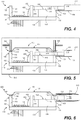
- FIG. 4 is a side cross-sectional view of the first section 110 of the enclosure 100 of FIG. 1 in which an optoelectronic device 402 and an end 410 of an optical fiber lead 412 are installed.
- the optoelectronic device 402 may include a detector, a light-emitting diode (LED), a laser diode or another optical device.
- the optoelectronic device 402 includes an optical surface 404 from which optical signals are transmitted, received, or both, depending on the nature of the optoelectronic device 402.
- the optoelectronic device 402 is joined by electrical leads 406 and the interface circuitry 126 to two or more of the conductive pins 124 to enable the optoelectronic device 402 to be electrically connected to systems or devices outside of the enclosure 100 of FIG. 1 once the enclosure 100 is sealed.
- the optoelectronic device 402 also may be mechanically secured to the base portion 120 of the first section 110, such as by an adhesive, solder, metal-to-ceramic brazing, or another physical coupling process or device (not shown in FIG. 4 ).
- positioning of the optoelectronic device 402 may be guided by the alignment body 156.
- the alignment body 156 may include an opening (as shown in illustrative embodiments of FIGS. 8B , 16A and related figures) into which the optoelectronic device 402 is position to facilitate alignment of the optical fiber lead 412 with the optical surface 404 of the optoelectronic device 402.
- the end 410 of the optical fiber lead 412 extends through the first wall 132 of the first wall portion 130 of the first section 110 of the enclosure 100 by passing through the open-ended slot 142 ( FIGS. 1 and 2 ) in the first wall 132.
- the end 410 of the optical fiber lead 412 may be received in the groove 158 in the alignment body 156 to align the end 410 of the optical fiber lead 412 with the optical surface 404 of the optoelectronic device 402 while the enclosure 1 00 is being assembled and sealed.
- the optical fiber lead 412 may be physically coupled to the first cable support member 150 using an adhesive 420 or another attachment process or device.
- the adhesive 420 may hold the optical fiber lead 412 in place while other steps are performed to hermetically seal the enclosure 100.
- the optical fiber lead 412 is a polymer-clad silica fiber having a silica core 418 and a hard polymer cladding 416.
- the adhesive 420 may secure the polymer cladding 416 or a portion of the silica core 418 to the first cable support member 150 and a portion of the silica core 418 may extend through the first wall 132 of the enclosure 100.
- the optical fiber lead 412 may include a metalized portion 414 located approximately at a point where the silica core 418 extends through the first wall 132 of the wall portion 130. The metalized portion 414 may sealingly engage the open-ended slot (not shown in FIG. 4 ) and the second edge 180 of the second section 160 of the enclosure 100 when the enclosure 100 is hermetically sealed, as described with reference to FIG. 5 .
- FIG. 5 is a side cross-sectional view of the first section 110 and the second section 160 of the enclosure 100 of FIG. 1 being hermetically sealed in a controlled atmosphere chamber 510.
- the controlled atmosphere chamber 510 may be filled with an inert gas (not shown in FIG. 5 ) so that the enclosure 100 will be filled with the inert gas after it is hermetically sealed.
- the insert gas environment may prevent condensation from forming on the optical surface 404 of the optoelectronic device 402 and/or on the end 410 of the optical fiber lead 412.
- heated sealing rollers 520 or another heated device may be applied to the second section 160 adjacent to the second edges 180.
- Application of the heated sealing rollers 520 causes the preformed solder layer 190 on the second edge 180 of the second section 160 of the enclosure 100 to melt.
- the melted, preformed solder layer 190 joins the second edge 180 of the second section 160 to the first edge 140 of the first section 110 and to the metalized portion 414 of the optical fiber lead 412.
- the enclosure 100 and the optical fiber lead 412 are hermetically sealed.
- FIG. 6 is a side cross-sectional view of a completed, hermetically sealed optical component 600 fitted with a cable strain relieve boot 610.
- the completed, hermetically sealed optical component 600 is sealed when it is removed from the controlled atmosphere chamber 510, with the first section 110, the second section 160, and the optical fiber lead 412 bonded together.
- adhesive 620 may be added between the optical fiber lead 412 and the second cable support member 166. The adhesive 620 may also fill an area between optical fiber leads when hermetically sealed optical component includes more than one optical fiber lead 412.
- the cable strain relief boot 610 may be moved into place over the optical fiber lead 412, the first cable support member 150, and the second cable support member 166.
- the completed, hermetically sealed optical component 600 may be ready for installation and use, e.g., by coupling a second end face of the optical fiber lead 412 to an optical fiber, such as a plastic optical fiber (e.g., a PMMA optical fiber).
- an optical fiber such as a plastic optical fiber (e.g., a PMMA optical fiber).
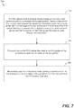
- FIG. 7 is a flow diagram of a particular embodiment of a method of forming a hermetically sealed optical component.
- a first portion of an optical fiber lead e.g., a portion of a polymer-clad silica fiber
- the first portion of the optical fiber lead is received and aligned with an optical surface of an optoelectronic device and the first portion of the optical cable extends through the wall portion.
- the enclosure 100 includes the base portion 120 to which the wall portion 130 is coupled around the perimeter 122 of the base portion 120.
- the end 410 of the optical fiber lead 412 is received at the open end 144 of the open-ended slot 142 in the first edge 140 of the wall portion 130 at the first wall 132.
- the end 410 of the optical fiber lead 412 is received in the alignment body 156 so that the end 410 is aligned with the optical surface 404 of the optoelectronic device 402 mounted in the first section 110 of the enclosure 100.
- the optical fiber lead is physically secured to the first portion of the enclosure outside the perimeter of the wall portion, at 704.
- the optical fiber lead 412 is secured to the first cable support member 150 of the first section 110 by the adhesive 420 to hold the optical fiber lead 412 in place while the enclosure 100 is hermetically sealed.
- the enclosure is hermetically sealed by fixably joining a second section of the enclosure to the first edge of the wall portion and to the first portion of the optical fiber lead, at 706. For example, as described with reference to FIG.
- the heated sealing rollers 520 may be applied adjacent to the second edge 180 of the second section 160 of the enclosure 100, causing the preformed solder layer 190 on the second edge 180 to bond the second section 160 with both the first edge 140 of the first section 110 of the enclosure 100 and to the metalized portion 414 of the optical fiber lead 412.
- FIGS. 8-15 illustrate formation of a hermetically sealed optical component including first types of optoelectronic device (i.e., a laser diode on a Kovar submount and a detector on a ceramic submount) and FIGS. 16-18 illustrate formation of a hermetically sealed optical component including second types of optoelectronic device (i.e., a laser and a detector in TO18 type headers).
- first and second types of optoelectronic devices are examples of commercially available optoelectronic devices that have different form factors.
- Embodiments disclosed herein enable assembly of hermetically sealed optical components using various form factors of optoelectronic devices, including the first type of optoelectronic device, the second type of optoelectronic device, and potentially other types optoelectronic devices.
- Each hermetically sealed optical component may have an align block that is designed for use with a particular form factor of optoelectronic device.
- Other constituent parts of the hermetically sealed optical components may be unchanged regardless of the form factor of the optoelectronic device or devices used.
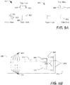
- FIG. 8A is top views of a particular embodiment of an enclosure body 800.
- the enclosure body 800 may correspond to the first section 110 of the enclosure 100 of FIGS. 1-6 .
- the enclosure body 800 may have two rows of 2x5 dual-in-line pins 824 for wire bonding to electronic components inside the enclosure body 800 (e.g., one or more optoelectronic devices and interface circuitry, as further described below).
- the pins 824 may be arranged in compliance with the industrial Multi-Source Agreement (MSA) standard.
- the enclosure body 800 may also include two mechanical package alignment posts 826 that are arranged in compliance with the industrial MSA standard.
- FIG. 8B is several views of a particular embodiment of a fiber alignment block 850.
- the fiber alignment block 850 may correspond to a particular embodiment of the alignment body of FIGS. 1-6 .
- the fiber alignment block 850 is shown from multiple views, including a top view, a side view, a back view (i.e., a view from the right side of the top view in the orientation illustrated of FIG. 8B ) and a front view (i.e., a view from the left side of the top view in the orientation illustrated in FIG. 8B ).
- the fiber alignment block 850 is formed using a high precision ceramic molding process.
- the enclosure body 800 includes two U-grooves 828 near a fiber snout 830.
- the U-grooves 828 may correspond to the open-ended slots 142 and 143 of FIGS. 1-6 and the fiber snout 830 may correspond to the first cable support member 150 of FIGS. 1-6 .
- the two U-grooves 828 are arranged to receive and facilitate alignment of two optical fiber leads (not shown in FIG. 8A ).
- the U-grooves 828 may have a width that corresponds to a diameter of a portion of the optical fiber leads that is to extend into the enclosure body 800.
- the dimensions and locations of the U-grooves 828 may be configured to accommodate two polymer-clad silica fibers, each with a 1 mm core diameter and a 3 mm diameter with an outer jacket.
- the enclosure body 800 may include one U-groove for each optical fiber lead.
- the fiber alignment block 850 may be configured to accommodate one or more optoelectronic devices, such as a detector and a laser (or another light source) mounted on precision submounts.
- the fiber alignment block 850 may include an opening 852 to receive and align each of the optoelectronic devices.
- the fiber alignment block 850 may also include a U-groove 854 with substantially the same width and depth as the U-grooves 828 of the enclosure body 800.
- the U-grooves 854 may be sized to receive polymer-clad silica fiber with a 1 mm core diameter.
- the openings 852 and the U-grooves 854 of the fiber alignment block 850 may be arranged such that when an optoelectronic device is positioned in one of the openings 852 and an optical fiber lead is positioned in the U-grooves 854 and 828, an end-face of the optical fiber lead is aligned with an optical surface of the optoelectronic device.
- FIG. 8C is several views of a particular embodiment of the fiber alignment block 850 of FIG. 8B within the enclosure body 800 of FIG. 8A .
- FIG. 8C shows a top view and a front view (from an end nearest the fiber snout 830) of the enclosure body 800 and fiber alignment block 850.
- the fiber alignment block 850 may be attached permanently to the enclosure body 800 (e.g., using high temperature blazing or another ceramic to metal bonding process).
- the U-grooves 828 of the enclosure body 800 wall and the U-grooves 854 of the fiber alignment block 850 may be precisely aligned for placement of optical fiber leads in a later processing step.
- FIG. 9A is several views of particular embodiments of optoelectronic devices 900 and 950.
- the optoelectronic devices 900 and 950 may be of the same type or may be different.
- a first optoelectronic device 900 may include an optical detector to receive signals and a second optoelectronic device 950 may include a light source to generate and send light signals.
- Each of the optoelectronic devices 900 and 950 may include an optical surface, such as a first optical surface 902 of the first optoelectronic device 900 and a second optical surface 952 of the second optoelectronic device 950.
- the first optical surface 902 may be arranged to detect light output from the optical fiber lead and the second optical surface 952 may be a light emitting surface of a laser or other light source to be coupled to the optical fiber lead.
- the optoelectronic devices 900 and 950 may each include a mounting surface, such as first mounting surface 904 of the first optoelectronic device 900 and a second mounting surface 954 of the second optoelectronic device 900.
- the optoelectronic devices 900 and 950 may be commercial off-the-shelf components. Accordingly, the mounting surfaces 904, 954 may have various configurations depending on which component is used. To illustrate, the mounting surfaces 904, 954 may formed of ceramic, a metal (e.g., Kovar), another material, or a combination thereof. In some embodiments, one or more of the mounting surfaces 904, 954 may include a submount.
- the submount of a particular optoelectronic device may be configured to adjust a height 908 of the optical surface of the particular optoelectronic device to align with the optical center of an optical fiber lead within a U-groove 854 of the fiber alignment block 850.
- a submount for a detector e.g., the first optoelectronic device 900
- the submount for a transmitter e.g., the second optoelectronic device 950
- Kovar or another metal or alloy to improve heat sink characteristics of the submount and to lower thermal resistance of the submount.
- FIG. 9B is a top view of a particular embodiment of the optoelectronic devices of FIG. 9A and interface circuitry 910 within the enclosure body 800 of FIG. 8C .
- the mounting surfaces 904, 954 of the optoelectronic devices 900, 950 have been mounted to an interior surface of the enclosure body 800.
- the optoelectronic devices 900, 950 are mounted within the openings 852 of the fiber alignment block 850.
- Each of the openings 852 has a width that corresponds to a width 906, 956 of the optoelectronic device 900, 950 to be mounted within the opening 852.
- the openings 852 guide installation of the optoelectronic devices 900, 950 in a manner that aligns each optical surface 902, 952 with a corresponding U-groove 854 of the fiber alignment block 850.
- the optoelectronic devices 900, 950 can be mounted on respective submounts in a manner that easily and precisely aligns them with the U-grooves 854 of the fiber alignment block 850 and the U-grooves 828 of the enclosure body 800.
- the optoelectronic devices 900, 950 are mounted to the enclosure body 800, the optoelectronic devices 900, 950 are attached (e.g., wire bonded) to interface circuit 910.
- the pins 824 connect the interface circuitry 910 to an external system (not shown) which inputs an electrical signal to drive the light source 950 and/or receives an electrical signal converted from the detector 900.
- FIG. 10 is a top view of a particular embodiment of an optical fiber lead 1000.
- the optical fiber lead 1000 may correspond to the optical fiber lead 412 of FIGS. 4-6 .
- the optical fiber lead 1000 may be a portion of a polymer-clad silica (PCS) optical fiber with a silica core 1018 and a polymer cladding with an outer jacket 1016. A portion of the silica core 1018 may be exposed.
- the optical fiber lead 1000 may also include a metalized portion 1014 over the exposed portion of the silica core 1018.
- PCS polymer-clad silica
- FIG. 11 is a top view of a particular embodiment of a pair of optical fiber leads 1000 of FIG. 10 inserted into the enclosure body 800 of FIG. 9B .
- Each of the optical fiber leads 1000 is placed into a corresponding U-groove of the fiber alignment block 850 and a correspond U-groove of the enclosure body 800.
- the metalized portion 1014 of each of the optical fiber leads 1000 may be fully embedded in the corresponding U-grooves of the fiber alignment block 850 and the enclosure body 800.
- the polymer cladding with the outer jacket 1016 of each of the optical fiber leads 1000 may be coupled to the fiber snout 830 of the enclosure body 800 using a quick cure adhesive 1102.
- the adhesive 1102 holds the optical fiber leads 1000 in place (e.g., inside the U-grooves) during subsequent manufacturing process steps.
- the optical fiber leads 1000 are automatically aligned to optical surfaces of the optoelectronic devices 900, 950 without using the active fiber alignment processes.
- the optical fiber leads 1000 may have a core diameter of about 1 mm (i.e., the diameter of the silica core 1018).
- the polymer cladding with the outer jacket 1016 may have an outer diameter of about 3 mm.
- the location and length of the metalized portion 1014 may be designed to match the U-groove of the enclosure body 800 and the U-groove of the fiber alignment block 850.
- the metalized portion 1014 may include gold (Au) and nickel (Ni) layers with thicknesses of about 0.2 micron and 4 micron, respectively. The Au/Ni layers facilitate sealing of the optical fiber leads 1000 to the enclosure body 800 in subsequent package hermetic sealing steps.
- FIG. 12 is a cross-sectional side view of a particular embodiment of the enclosure body 800 of FIG. 11 and an enclosure top 1200.
- the enclosure top 1200 may be sealed to the enclosure body 800.
- a bottom portion of the enclosure top 1200 may include or be coupled to a layer of solder 1202 for package sealing.
- the solder 1202 may be coated on the bottom portion of enclosure top 1200 as a solder perform.
- the solder 1202 may be Au/Sn solder to make a high reliability solder joint.
- the melting temperature of the Au/Sn solder may be about 280 degree C, which is higher than most of the commonly used solder alloys.
- a high temperature lid seal process may be used to form reliable hermetic package with the Au/Sn solder.
- the metalized portion 1014 of the optical fiber lead 1000 may be subject to significant heating during the high temperature lid seal process. Accordingly, the metalized portion 1014 is applied over the silica core 1018, which can withstand the heating more readily than the polymer cladding with the outer jacket 1016 can.
- FIG. 13 is a cross-sectional side view of a particular embodiment of the enclosure top 1200 of FIG. 12 being sealed to the enclosure body 800 of FIG. 12 by sealing rollers 1300.
- a seam sealer may be used to melt the solder 1202.
- a pair of parallel seam sealing rollers 1300 may be moved along the edges of the enclosure top 1200.
- the sealing rollers 1300 may be heated to about 300 degree C as they move along the edges of the enclosure top 1200.
- the solder 1202 may reflow over the U-grooves and the metalized portion 1014 of the optical fiber leads.
- the solder 1202 may fill the U-grooves with melted solder. After the sealing rollers 1300 complete their movement along the edges of the enclosure top 1200, heating stops and the solder 1202 solidifies forming a hermetic seal between the enclosure top 1200, the enclosure body 800 and the optical fiber leads.
- the seam sealing process may be performed in a controlled environment, such as inside a dry enclosure filled with an inert gas (e.g., nitrogen). Thus, an interior of the hermetically sealed enclosure body may be filled with the inert gas.
- an inert gas e.g., nitrogen
- FIG. 14 is several views of a particular embodiment of the sealed enclosure body 800 and enclosure top 1 200 of FIG. 13 .
- additional adhesive e.g., epoxy
- fiber snout 830 for fiber strain relieve.
- FIG. 15 is side cross-sectional view of a particular embodiment of the sealed enclosure body 800 and enclosure top 1200 of FIG. 14 with a fiber boot 1500 forming a complete, hermetically sealed optical component.
- the fiber boot 1500 may be installed on the fiber snout 830.
- the fiber boot 1500 may support an outer jacket of the optical fiber lead 1000.
- the fiber boot 1500 may also protects the optical fiber lead 1000 from bending more than its allowable bend radius.
- one or more optoelectronic devices used to form a hermetically sealed optical component may be in a TO18 package.
- a fiber alignment block may be adapted to receive the TO18 package and to facilitate alignment of the optoelectronic devices with optical fiber leads.
- an enclosure top may be taller to accommodate the TO18 package.
- FIGS. 16-18 illustrate embodiments of forming a hermetically sealed optical component using optoelectronic devices in TO18 packages (also call TO headers).
- FIGS. 16-18 certain components are similar to components described above with reference to FIGS. 8-15 . Accordingly, detailed description of those components is omitted. Reference numerals that are used in FIGS. 8-15 are also used in FIGS. 16-18 to denote elements that are the same or similar with minor variations.
- FIG. 16A is several views of a particular embodiment of a fiber alignment block 1650.
- fiber alignment block 1650 may correspond to the alignment body 156 of FIGS. 1-6 .
- the fiber alignment block 1650 is shown from multiple views, including a top view, a cross-sectional side view, a back view (i.e., a view from the right side of the top view in the orientation illustrated of FIG. 16A ) and a front view (i.e., a view from the left side of the top view in the orientation illustrated in FIG. 16A ).
- the fiber alignment block 1650 is formed using a high precision ceramic molding process.
- the fiber alignment block 1650 may be adapted to receive optoelectronic devices, e.g., a detector and a laser, in TO18 packages, at openings 1652.
- a location and a size of fiber alignment U-grooves 1654 may be substantially the same as the U-grooves 854 of the fiber alignment block 850 of FIG. 8B ; however, a front side 1656 of the fiber alignment block 1650 may be taller to accommodate the TO18 packages and to align the optoelectronic devices with centers of the U-grooves 1654.
- FIG. 16B is a top views of a particular embodiment of the fiber alignment block 1650 of FIG. 16A within the enclosure body 800 of FIG. 8A .
- the fiber alignment block 1650 may be attached permanently to the enclosure body 800 (e.g., using high temperature blazing or another ceramic to metal bonding process).
- the U-grooves 828 of the enclosure body 800 wall and the U-grooves 1654 of the fiber alignment block 1650 may be precisely aligned for placement of optical fiber leads in a later processing step.
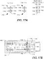
- FIG. 17A is several views of particular embodiments of optoelectronic devices 1700 and 1750 in TO18 packaging.
- the optoelectronic devices 1700 and 1750 may be of the same type or may be of different types.
- a first optoelectronic device 1700 may include an optical detector to receive signals and a second optoelectronic device 1750 may include a light source to generate and send light signals.
- Each of the optoelectronic devices 1700 and 1750 may include an optical surface, such as a first optical surface 1704 of the first optoelectronic device 1700 and a second optical surface 1754 of the second optoelectronic device 1750.
- the first optical surface 1704 may be arranged to detect light of a light based signal and the second optical surface 1754 may be a light emitting surface of a laser or other light source.
- Each of the optoelectronic devices 1700 and 1750 may include a TO18 header 1702, 1752 and leads 1706, 1756, respectively.
- the TO18 headers 1702, 1752 may be received into the fiber alignment block 1 650 in alignment with the U-grooves 1654 of the fiber alignment block 1650.
- the leads 1706, 1756 may be electrically coupled to the pins 824 via the interface circuitry 910 (e.g., via wire bonding).
- FIG. 18 is a top view of a particular embodiment of the optical fiber leads 1 000 of FIG. 10 inserted into the enclosure body of FIG. 17B .
- the optical fiber leads 1000 are automatically aligned with the optoelectronic components 1700, 1750.
- the optical fiber leads 1000 may be coupled to the enclosure body 800 using an adhesive 1802, which holds the optical fiber leads 1000 in place (e.g., inside the U-grooves) during subsequent manufacturing process steps.
- the subsequent manufacturing process steps may be performed in the same manner as described with reference to FIGS. 12-15 .
- an enclosure top (sized to accommodate the fiber alignment block 1650) may be placed over the enclosure body 800 and seam sealed to hermetically seal the enclosure body 800, the enclosure top, and the optical fiber leads 1000.
- Adhesive may be backfilled into the fiber snout of the enclosure body, and a fiber boot may be positioned over the optical fiber leads and the fiber snout.
- hermetically sealed optical components can be manufactured using processes disclosed herein.
- the hermetically sealed optical components may be well suited to coupling to PMM A plastic optical fibers since the core and cladding diameters of the optical fiber leads used provide relatively low coupling losses when the hermetically sealed optical components are coupled to PMMA plastic optical fibers.
- the hermetically sealed optical components may include transmitters, receivers, transceivers or other optical or optoelectronic devices.
Landscapes
- Physics & Mathematics (AREA)
- General Physics & Mathematics (AREA)
- Optics & Photonics (AREA)
- Optical Couplings Of Light Guides (AREA)
- Led Device Packages (AREA)
- Semiconductor Lasers (AREA)
Applications Claiming Priority (2)
| Application Number | Priority Date | Filing Date | Title |
|---|---|---|---|
| US13/227,428 US8596886B2 (en) | 2011-09-07 | 2011-09-07 | Hermetic small form factor optical device packaging for plastic optical fiber networks |
| PCT/US2012/049634 WO2013036338A1 (en) | 2011-09-07 | 2012-08-03 | Hermetic small form factor optical device packaging for plastic optical fiber networks |
Publications (2)
| Publication Number | Publication Date |
|---|---|
| EP2753964A1 EP2753964A1 (en) | 2014-07-16 |
| EP2753964B1 true EP2753964B1 (en) | 2020-10-07 |
Family
ID=46851580
Family Applications (1)
| Application Number | Title | Priority Date | Filing Date |
|---|---|---|---|
| EP12759291.3A Active EP2753964B1 (en) | 2011-09-07 | 2012-08-03 | Hermetic small form factor optical device packaging for plastic optical fiber networks |
Country Status (5)
| Country | Link |
|---|---|
| US (1) | US8596886B2 (enExample) |
| EP (1) | EP2753964B1 (enExample) |
| JP (1) | JP6086914B2 (enExample) |
| CN (1) | CN103782212B (enExample) |
| WO (1) | WO2013036338A1 (enExample) |
Families Citing this family (6)
| Publication number | Priority date | Publication date | Assignee | Title |
|---|---|---|---|---|
| US10572423B2 (en) | 2013-05-17 | 2020-02-25 | The Boeing Company | Systems and methods of data communication |
| DE102014101794B4 (de) * | 2014-02-13 | 2020-02-13 | Hanon Systems | Vorrichtung zur Expansion von Kältemittel |
| CN109416446B (zh) * | 2016-10-11 | 2020-09-25 | 华为技术有限公司 | 一种光收发组件 |
| US20190278036A1 (en) * | 2018-03-07 | 2019-09-12 | Lightwave Logic Inc. | Embedded hermetic capsule and method |
| US11029475B2 (en) * | 2019-04-08 | 2021-06-08 | Cisco Technology, Inc. | Frame lid for in-package optics |
| CN113745963A (zh) * | 2020-05-29 | 2021-12-03 | 方强 | 防止光纤耦合半导体激光模块壳体产生冷凝水的装置 |
Citations (1)
| Publication number | Priority date | Publication date | Assignee | Title |
|---|---|---|---|---|
| EP1596233A1 (en) * | 2003-02-19 | 2005-11-16 | Hamamatsu Photonics K. K. | Optical module |
Family Cites Families (25)
| Publication number | Priority date | Publication date | Assignee | Title |
|---|---|---|---|---|
| US4307934A (en) | 1978-05-08 | 1981-12-29 | General Dynamics, Pomona Division | Packaged fiber optic modules |
| JPH04191706A (ja) * | 1990-11-27 | 1992-07-10 | Mitsubishi Rayon Co Ltd | 光フアイバ及びその製造法 |
| US5212762A (en) * | 1990-11-27 | 1993-05-18 | Mitsubishi Rayon Co., Ltd. | Plastic-clad silica (PCS) fibers and methods and apparatuses for producing the same |
| US5202943A (en) | 1991-10-04 | 1993-04-13 | International Business Machines Corporation | Optoelectronic assembly with alignment member |
| SE9403574L (sv) * | 1994-10-19 | 1996-04-20 | Ericsson Telefon Ab L M | Optokomponentkapsel med optiskt gränssnitt |
| JPH09318849A (ja) * | 1996-05-24 | 1997-12-12 | Fujitsu Ltd | 光伝送モジュールおよびその製造方法 |
| US5745624A (en) | 1996-08-23 | 1998-04-28 | The Boeing Company | Automatic alignment and locking method and apparatus for fiber optic module manufacturing |
| JP2943760B2 (ja) | 1997-04-18 | 1999-08-30 | 日本電気株式会社 | 光ファイバ導入部の気密封止方法及び気密封止構造 |
| US6056447A (en) * | 1998-04-06 | 2000-05-02 | Lucent Technologies, Inc. | Covariant optical module |
| JP2000019360A (ja) * | 1998-07-03 | 2000-01-21 | Hitachi Ltd | 光モジュール |
| US6888169B2 (en) | 2000-09-29 | 2005-05-03 | Optical Communication Products, Inc. | High speed optical subassembly with ceramic carrier |
| DE10112274B4 (de) | 2001-03-14 | 2006-05-24 | Finisar Corp.(N.D.Ges.D.Staates Delaware), Sunnyvale | Optoelektonisches Sendemodul und Verfahren zu dessen Herstellung |
| US20030053169A1 (en) | 2001-06-07 | 2003-03-20 | The Furukawa Electric Co., Ltd. | Optical transmitter, WDM optical transmission device and optical module |
| FR2830087B1 (fr) | 2001-09-27 | 2003-12-19 | Cit Alcatel | Fibre optique silice a double gaine polymere |
| US6757308B1 (en) | 2002-05-22 | 2004-06-29 | Optical Communication Products, Inc. | Hermetically sealed transmitter optical subassembly |
| US6827505B2 (en) | 2002-12-16 | 2004-12-07 | International Business Machines Corporation | Optoelectronic package structure and process for planar passive optical and optoelectronic devices |
| US20040240804A1 (en) | 2003-06-02 | 2004-12-02 | Amaresh Mahapatra | Liquid crystal polymer clad optical fiber and its use in hermetic packaging |
| US6900509B2 (en) | 2003-09-19 | 2005-05-31 | Agilent Technologies, Inc. | Optical receiver package |
| US7309174B2 (en) | 2004-01-22 | 2007-12-18 | Finisar Corporation | Integrated optical devices and methods of making same |
| JP2006066875A (ja) * | 2004-07-26 | 2006-03-09 | Fuji Photo Film Co Ltd | レーザモジュール |
| WO2008111218A1 (ja) | 2007-03-15 | 2008-09-18 | Ibiden Co., Ltd. | 熱電変換装置 |
| US7841781B2 (en) | 2007-08-29 | 2010-11-30 | Avago Technologies Fiber Ip (Singapore) Pte. Ltd. | Methods and apparatuses for providing a hermetic sealing system for an optical transceiver module |
| JP5216714B2 (ja) * | 2009-02-25 | 2013-06-19 | 矢崎総業株式会社 | 1芯双方向光通信モジュール及び1芯双方向光通信コネクタ |
| JP2010237636A (ja) | 2009-03-12 | 2010-10-21 | Toshiba Corp | 光リンク装置及びその製造方法 |
| JP2010217323A (ja) * | 2009-03-13 | 2010-09-30 | Fujikura Ltd | 光結合構造および光送受信モジュール |
-
2011
- 2011-09-07 US US13/227,428 patent/US8596886B2/en active Active
-
2012
- 2012-08-03 WO PCT/US2012/049634 patent/WO2013036338A1/en not_active Ceased
- 2012-08-03 EP EP12759291.3A patent/EP2753964B1/en active Active
- 2012-08-03 JP JP2014529719A patent/JP6086914B2/ja active Active
- 2012-08-03 CN CN201280043536.0A patent/CN103782212B/zh active Active
Patent Citations (1)
| Publication number | Priority date | Publication date | Assignee | Title |
|---|---|---|---|---|
| EP1596233A1 (en) * | 2003-02-19 | 2005-11-16 | Hamamatsu Photonics K. K. | Optical module |
Also Published As
| Publication number | Publication date |
|---|---|
| CN103782212B (zh) | 2018-08-07 |
| EP2753964A1 (en) | 2014-07-16 |
| CN103782212A (zh) | 2014-05-07 |
| WO2013036338A1 (en) | 2013-03-14 |
| JP6086914B2 (ja) | 2017-03-01 |
| US20130058617A1 (en) | 2013-03-07 |
| JP2014525609A (ja) | 2014-09-29 |
| US8596886B2 (en) | 2013-12-03 |
Similar Documents
| Publication | Publication Date | Title |
|---|---|---|
| US9442255B2 (en) | Low profile fiber-to-module interface with relaxed alignment tolerances | |
| EP2753964B1 (en) | Hermetic small form factor optical device packaging for plastic optical fiber networks | |
| US8079125B2 (en) | Manufacturing method of multi-channel optical module | |
| US9151916B2 (en) | Compact optical package made with planar structures | |
| JP4180537B2 (ja) | 光学素子の封止構造体および光結合器ならびに光学素子の封止方法 | |
| US7629537B2 (en) | Single layer flex circuit | |
| KR100411577B1 (ko) | 광섬유 접속부 및 그것의 사용 방법 | |
| CN100516953C (zh) | 具有集成柔性电路的小型光学分组件 | |
| JPWO1998045741A1 (ja) | 光モジュール、光モジュールの製造方法及び光伝送装置 | |
| WO1998045741A1 (fr) | Module optique, procede de fabrication d'un module optique, et dispositif optique de transmission | |
| CN104169767A (zh) | 透镜部件以及具备该透镜部件的光学模块 | |
| US9052476B2 (en) | Wafer-level packaged optical subassembly and transceiver module having same | |
| CN101303439A (zh) | 光学组件及其形成方法 | |
| WO2013097449A1 (zh) | 一种光电子器件的光导纤维的安装固定结构 | |
| US7268368B1 (en) | Semiconductor package having optical receptacles and light transmissive/opaque portions and method of making same | |
| US20040240803A1 (en) | Use of chip-on-board technology to mount optical transmitting and detecting devices with a protective covering with multiple optical interface options | |
| US7419311B2 (en) | Surface mount optical coupler, method of mounting the same, and method of producing the same | |
| EP1722258A1 (en) | Optical radiation coupling module | |
| US9297967B2 (en) | Device for converting signal | |
| US20100002984A1 (en) | Optical waveguide device | |
| JP5297870B2 (ja) | 光モジュールの製造方法 | |
| US8581173B2 (en) | Fiber optic transceiver module having a molded cover in which an optical beam transformer made of an elastomer is integrally formed | |
| JP2013231895A (ja) | 光モジュール | |
| JP2007333912A (ja) | 光モジュール | |
| JP4744268B2 (ja) | 光モジュール |
Legal Events
| Date | Code | Title | Description |
|---|---|---|---|
| PUAI | Public reference made under article 153(3) epc to a published international application that has entered the european phase |
Free format text: ORIGINAL CODE: 0009012 |
|
| 17P | Request for examination filed |
Effective date: 20140331 |
|
| AK | Designated contracting states |
Kind code of ref document: A1 Designated state(s): AL AT BE BG CH CY CZ DE DK EE ES FI FR GB GR HR HU IE IS IT LI LT LU LV MC MK MT NL NO PL PT RO RS SE SI SK SM TR |
|
| DAX | Request for extension of the european patent (deleted) | ||
| 17Q | First examination report despatched |
Effective date: 20160923 |
|
| STAA | Information on the status of an ep patent application or granted ep patent |
Free format text: STATUS: EXAMINATION IS IN PROGRESS |
|
| GRAP | Despatch of communication of intention to grant a patent |
Free format text: ORIGINAL CODE: EPIDOSNIGR1 |
|
| STAA | Information on the status of an ep patent application or granted ep patent |
Free format text: STATUS: GRANT OF PATENT IS INTENDED |
|
| INTG | Intention to grant announced |
Effective date: 20191105 |
|
| GRAJ | Information related to disapproval of communication of intention to grant by the applicant or resumption of examination proceedings by the epo deleted |
Free format text: ORIGINAL CODE: EPIDOSDIGR1 |
|
| STAA | Information on the status of an ep patent application or granted ep patent |
Free format text: STATUS: EXAMINATION IS IN PROGRESS |
|
| GRAP | Despatch of communication of intention to grant a patent |
Free format text: ORIGINAL CODE: EPIDOSNIGR1 |
|
| STAA | Information on the status of an ep patent application or granted ep patent |
Free format text: STATUS: GRANT OF PATENT IS INTENDED |
|
| INTC | Intention to grant announced (deleted) | ||
| INTG | Intention to grant announced |
Effective date: 20200324 |
|
| GRAS | Grant fee paid |
Free format text: ORIGINAL CODE: EPIDOSNIGR3 |
|
| GRAA | (expected) grant |
Free format text: ORIGINAL CODE: 0009210 |
|
| STAA | Information on the status of an ep patent application or granted ep patent |
Free format text: STATUS: THE PATENT HAS BEEN GRANTED |
|
| AK | Designated contracting states |
Kind code of ref document: B1 Designated state(s): AL AT BE BG CH CY CZ DE DK EE ES FI FR GB GR HR HU IE IS IT LI LT LU LV MC MK MT NL NO PL PT RO RS SE SI SK SM TR |
|
| REG | Reference to a national code |
Ref country code: GB Ref legal event code: FG4D |
|
| REG | Reference to a national code |
Ref country code: CH Ref legal event code: EP Ref country code: AT Ref legal event code: REF Ref document number: 1321765 Country of ref document: AT Kind code of ref document: T Effective date: 20201015 |
|
| REG | Reference to a national code |
Ref country code: DE Ref legal event code: R096 Ref document number: 602012072685 Country of ref document: DE |
|
| REG | Reference to a national code |
Ref country code: IE Ref legal event code: FG4D |
|
| REG | Reference to a national code |
Ref country code: NL Ref legal event code: MP Effective date: 20201007 |
|
| REG | Reference to a national code |
Ref country code: AT Ref legal event code: MK05 Ref document number: 1321765 Country of ref document: AT Kind code of ref document: T Effective date: 20201007 |
|
| PG25 | Lapsed in a contracting state [announced via postgrant information from national office to epo] |
Ref country code: GR Free format text: LAPSE BECAUSE OF FAILURE TO SUBMIT A TRANSLATION OF THE DESCRIPTION OR TO PAY THE FEE WITHIN THE PRESCRIBED TIME-LIMIT Effective date: 20210108 Ref country code: RS Free format text: LAPSE BECAUSE OF FAILURE TO SUBMIT A TRANSLATION OF THE DESCRIPTION OR TO PAY THE FEE WITHIN THE PRESCRIBED TIME-LIMIT Effective date: 20201007 Ref country code: FI Free format text: LAPSE BECAUSE OF FAILURE TO SUBMIT A TRANSLATION OF THE DESCRIPTION OR TO PAY THE FEE WITHIN THE PRESCRIBED TIME-LIMIT Effective date: 20201007 Ref country code: NL Free format text: LAPSE BECAUSE OF FAILURE TO SUBMIT A TRANSLATION OF THE DESCRIPTION OR TO PAY THE FEE WITHIN THE PRESCRIBED TIME-LIMIT Effective date: 20201007 Ref country code: PT Free format text: LAPSE BECAUSE OF FAILURE TO SUBMIT A TRANSLATION OF THE DESCRIPTION OR TO PAY THE FEE WITHIN THE PRESCRIBED TIME-LIMIT Effective date: 20210208 Ref country code: NO Free format text: LAPSE BECAUSE OF FAILURE TO SUBMIT A TRANSLATION OF THE DESCRIPTION OR TO PAY THE FEE WITHIN THE PRESCRIBED TIME-LIMIT Effective date: 20210107 |
|
| REG | Reference to a national code |
Ref country code: LT Ref legal event code: MG4D |
|
| PG25 | Lapsed in a contracting state [announced via postgrant information from national office to epo] |
Ref country code: PL Free format text: LAPSE BECAUSE OF FAILURE TO SUBMIT A TRANSLATION OF THE DESCRIPTION OR TO PAY THE FEE WITHIN THE PRESCRIBED TIME-LIMIT Effective date: 20201007 Ref country code: LV Free format text: LAPSE BECAUSE OF FAILURE TO SUBMIT A TRANSLATION OF THE DESCRIPTION OR TO PAY THE FEE WITHIN THE PRESCRIBED TIME-LIMIT Effective date: 20201007 Ref country code: SE Free format text: LAPSE BECAUSE OF FAILURE TO SUBMIT A TRANSLATION OF THE DESCRIPTION OR TO PAY THE FEE WITHIN THE PRESCRIBED TIME-LIMIT Effective date: 20201007 Ref country code: IS Free format text: LAPSE BECAUSE OF FAILURE TO SUBMIT A TRANSLATION OF THE DESCRIPTION OR TO PAY THE FEE WITHIN THE PRESCRIBED TIME-LIMIT Effective date: 20210207 Ref country code: ES Free format text: LAPSE BECAUSE OF FAILURE TO SUBMIT A TRANSLATION OF THE DESCRIPTION OR TO PAY THE FEE WITHIN THE PRESCRIBED TIME-LIMIT Effective date: 20201007 Ref country code: AT Free format text: LAPSE BECAUSE OF FAILURE TO SUBMIT A TRANSLATION OF THE DESCRIPTION OR TO PAY THE FEE WITHIN THE PRESCRIBED TIME-LIMIT Effective date: 20201007 Ref country code: BG Free format text: LAPSE BECAUSE OF FAILURE TO SUBMIT A TRANSLATION OF THE DESCRIPTION OR TO PAY THE FEE WITHIN THE PRESCRIBED TIME-LIMIT Effective date: 20210107 |
|
| PG25 | Lapsed in a contracting state [announced via postgrant information from national office to epo] |
Ref country code: HR Free format text: LAPSE BECAUSE OF FAILURE TO SUBMIT A TRANSLATION OF THE DESCRIPTION OR TO PAY THE FEE WITHIN THE PRESCRIBED TIME-LIMIT Effective date: 20201007 |
|
| REG | Reference to a national code |
Ref country code: DE Ref legal event code: R097 Ref document number: 602012072685 Country of ref document: DE |
|
| PG25 | Lapsed in a contracting state [announced via postgrant information from national office to epo] |
Ref country code: EE Free format text: LAPSE BECAUSE OF FAILURE TO SUBMIT A TRANSLATION OF THE DESCRIPTION OR TO PAY THE FEE WITHIN THE PRESCRIBED TIME-LIMIT Effective date: 20201007 Ref country code: CZ Free format text: LAPSE BECAUSE OF FAILURE TO SUBMIT A TRANSLATION OF THE DESCRIPTION OR TO PAY THE FEE WITHIN THE PRESCRIBED TIME-LIMIT Effective date: 20201007 Ref country code: SM Free format text: LAPSE BECAUSE OF FAILURE TO SUBMIT A TRANSLATION OF THE DESCRIPTION OR TO PAY THE FEE WITHIN THE PRESCRIBED TIME-LIMIT Effective date: 20201007 Ref country code: LT Free format text: LAPSE BECAUSE OF FAILURE TO SUBMIT A TRANSLATION OF THE DESCRIPTION OR TO PAY THE FEE WITHIN THE PRESCRIBED TIME-LIMIT Effective date: 20201007 Ref country code: SK Free format text: LAPSE BECAUSE OF FAILURE TO SUBMIT A TRANSLATION OF THE DESCRIPTION OR TO PAY THE FEE WITHIN THE PRESCRIBED TIME-LIMIT Effective date: 20201007 Ref country code: RO Free format text: LAPSE BECAUSE OF FAILURE TO SUBMIT A TRANSLATION OF THE DESCRIPTION OR TO PAY THE FEE WITHIN THE PRESCRIBED TIME-LIMIT Effective date: 20201007 |
|
| PLBE | No opposition filed within time limit |
Free format text: ORIGINAL CODE: 0009261 |
|
| STAA | Information on the status of an ep patent application or granted ep patent |
Free format text: STATUS: NO OPPOSITION FILED WITHIN TIME LIMIT |
|
| PG25 | Lapsed in a contracting state [announced via postgrant information from national office to epo] |
Ref country code: DK Free format text: LAPSE BECAUSE OF FAILURE TO SUBMIT A TRANSLATION OF THE DESCRIPTION OR TO PAY THE FEE WITHIN THE PRESCRIBED TIME-LIMIT Effective date: 20201007 |
|
| 26N | No opposition filed |
Effective date: 20210708 |
|
| PG25 | Lapsed in a contracting state [announced via postgrant information from national office to epo] |
Ref country code: AL Free format text: LAPSE BECAUSE OF FAILURE TO SUBMIT A TRANSLATION OF THE DESCRIPTION OR TO PAY THE FEE WITHIN THE PRESCRIBED TIME-LIMIT Effective date: 20201007 Ref country code: IT Free format text: LAPSE BECAUSE OF FAILURE TO SUBMIT A TRANSLATION OF THE DESCRIPTION OR TO PAY THE FEE WITHIN THE PRESCRIBED TIME-LIMIT Effective date: 20201007 |
|
| PG25 | Lapsed in a contracting state [announced via postgrant information from national office to epo] |
Ref country code: SI Free format text: LAPSE BECAUSE OF FAILURE TO SUBMIT A TRANSLATION OF THE DESCRIPTION OR TO PAY THE FEE WITHIN THE PRESCRIBED TIME-LIMIT Effective date: 20201007 |
|
| REG | Reference to a national code |
Ref country code: CH Ref legal event code: PL |
|
| PG25 | Lapsed in a contracting state [announced via postgrant information from national office to epo] |
Ref country code: MC Free format text: LAPSE BECAUSE OF FAILURE TO SUBMIT A TRANSLATION OF THE DESCRIPTION OR TO PAY THE FEE WITHIN THE PRESCRIBED TIME-LIMIT Effective date: 20201007 |
|
| REG | Reference to a national code |
Ref country code: BE Ref legal event code: MM Effective date: 20210831 |
|
| PG25 | Lapsed in a contracting state [announced via postgrant information from national office to epo] |
Ref country code: LI Free format text: LAPSE BECAUSE OF NON-PAYMENT OF DUE FEES Effective date: 20210831 Ref country code: CH Free format text: LAPSE BECAUSE OF NON-PAYMENT OF DUE FEES Effective date: 20210831 |
|
| PG25 | Lapsed in a contracting state [announced via postgrant information from national office to epo] |
Ref country code: IS Free format text: LAPSE BECAUSE OF FAILURE TO SUBMIT A TRANSLATION OF THE DESCRIPTION OR TO PAY THE FEE WITHIN THE PRESCRIBED TIME-LIMIT Effective date: 20210207 Ref country code: LU Free format text: LAPSE BECAUSE OF NON-PAYMENT OF DUE FEES Effective date: 20210803 |
|
| PG25 | Lapsed in a contracting state [announced via postgrant information from national office to epo] |
Ref country code: IE Free format text: LAPSE BECAUSE OF NON-PAYMENT OF DUE FEES Effective date: 20210803 Ref country code: BE Free format text: LAPSE BECAUSE OF NON-PAYMENT OF DUE FEES Effective date: 20210831 |
|
| PG25 | Lapsed in a contracting state [announced via postgrant information from national office to epo] |
Ref country code: HU Free format text: LAPSE BECAUSE OF FAILURE TO SUBMIT A TRANSLATION OF THE DESCRIPTION OR TO PAY THE FEE WITHIN THE PRESCRIBED TIME-LIMIT; INVALID AB INITIO Effective date: 20120803 Ref country code: CY Free format text: LAPSE BECAUSE OF FAILURE TO SUBMIT A TRANSLATION OF THE DESCRIPTION OR TO PAY THE FEE WITHIN THE PRESCRIBED TIME-LIMIT Effective date: 20201007 |
|
| P01 | Opt-out of the competence of the unified patent court (upc) registered |
Effective date: 20230516 |
|
| PG25 | Lapsed in a contracting state [announced via postgrant information from national office to epo] |
Ref country code: MK Free format text: LAPSE BECAUSE OF FAILURE TO SUBMIT A TRANSLATION OF THE DESCRIPTION OR TO PAY THE FEE WITHIN THE PRESCRIBED TIME-LIMIT Effective date: 20201007 |
|
| PG25 | Lapsed in a contracting state [announced via postgrant information from national office to epo] |
Ref country code: MT Free format text: LAPSE BECAUSE OF FAILURE TO SUBMIT A TRANSLATION OF THE DESCRIPTION OR TO PAY THE FEE WITHIN THE PRESCRIBED TIME-LIMIT Effective date: 20201007 |
|
| PGFP | Annual fee paid to national office [announced via postgrant information from national office to epo] |
Ref country code: DE Payment date: 20250827 Year of fee payment: 14 |
|
| PGFP | Annual fee paid to national office [announced via postgrant information from national office to epo] |
Ref country code: GB Payment date: 20250827 Year of fee payment: 14 |
|
| PGFP | Annual fee paid to national office [announced via postgrant information from national office to epo] |
Ref country code: FR Payment date: 20250825 Year of fee payment: 14 |
|
| PG25 | Lapsed in a contracting state [announced via postgrant information from national office to epo] |
Ref country code: TR Free format text: LAPSE BECAUSE OF FAILURE TO SUBMIT A TRANSLATION OF THE DESCRIPTION OR TO PAY THE FEE WITHIN THE PRESCRIBED TIME-LIMIT Effective date: 20201007 |