EP2748924B1 - Radio frequency power amplifier circuit and method - Google Patents
Radio frequency power amplifier circuit and method Download PDFInfo
- Publication number
- EP2748924B1 EP2748924B1 EP12714304.8A EP12714304A EP2748924B1 EP 2748924 B1 EP2748924 B1 EP 2748924B1 EP 12714304 A EP12714304 A EP 12714304A EP 2748924 B1 EP2748924 B1 EP 2748924B1
- Authority
- EP
- European Patent Office
- Prior art keywords
- signal
- input
- radio frequency
- output
- amplifier
- Prior art date
- Legal status (The legal status is an assumption and is not a legal conclusion. Google has not performed a legal analysis and makes no representation as to the accuracy of the status listed.)
- Not-in-force
Links
Images





Classifications
-
- H—ELECTRICITY
- H03—ELECTRONIC CIRCUITRY
- H03F—AMPLIFIERS
- H03F3/00—Amplifiers with only discharge tubes or only semiconductor devices as amplifying elements
- H03F3/20—Power amplifiers, e.g. Class B amplifiers, Class C amplifiers
- H03F3/21—Power amplifiers, e.g. Class B amplifiers, Class C amplifiers with semiconductor devices only
- H03F3/211—Power amplifiers, e.g. Class B amplifiers, Class C amplifiers with semiconductor devices only using a combination of several amplifiers
-
- H—ELECTRICITY
- H03—ELECTRONIC CIRCUITRY
- H03F—AMPLIFIERS
- H03F1/00—Details of amplifiers with only discharge tubes, only semiconductor devices or only unspecified devices as amplifying elements
- H03F1/02—Modifications of amplifiers to raise the efficiency, e.g. gliding Class A stages, use of an auxiliary oscillation
- H03F1/0205—Modifications of amplifiers to raise the efficiency, e.g. gliding Class A stages, use of an auxiliary oscillation in transistor amplifiers
- H03F1/0211—Modifications of amplifiers to raise the efficiency, e.g. gliding Class A stages, use of an auxiliary oscillation in transistor amplifiers with control of the supply voltage or current
- H03F1/0216—Continuous control
- H03F1/0233—Continuous control by using a signal derived from the output signal, e.g. bootstrapping the voltage supply
-
- H—ELECTRICITY
- H03—ELECTRONIC CIRCUITRY
- H03F—AMPLIFIERS
- H03F1/00—Details of amplifiers with only discharge tubes, only semiconductor devices or only unspecified devices as amplifying elements
- H03F1/02—Modifications of amplifiers to raise the efficiency, e.g. gliding Class A stages, use of an auxiliary oscillation
- H03F1/0205—Modifications of amplifiers to raise the efficiency, e.g. gliding Class A stages, use of an auxiliary oscillation in transistor amplifiers
- H03F1/0288—Modifications of amplifiers to raise the efficiency, e.g. gliding Class A stages, use of an auxiliary oscillation in transistor amplifiers using a main and one or several auxiliary peaking amplifiers whereby the load is connected to the main amplifier using an impedance inverter, e.g. Doherty amplifiers
-
- H—ELECTRICITY
- H03—ELECTRONIC CIRCUITRY
- H03F—AMPLIFIERS
- H03F3/00—Amplifiers with only discharge tubes or only semiconductor devices as amplifying elements
- H03F3/189—High-frequency amplifiers, e.g. radio frequency amplifiers
- H03F3/19—High-frequency amplifiers, e.g. radio frequency amplifiers with semiconductor devices only
- H03F3/193—High-frequency amplifiers, e.g. radio frequency amplifiers with semiconductor devices only with field-effect devices
-
- H—ELECTRICITY
- H03—ELECTRONIC CIRCUITRY
- H03F—AMPLIFIERS
- H03F2200/00—Indexing scheme relating to amplifiers
- H03F2200/102—A non-specified detector of a signal envelope being used in an amplifying circuit
-
- H—ELECTRICITY
- H03—ELECTRONIC CIRCUITRY
- H03F—AMPLIFIERS
- H03F2200/00—Indexing scheme relating to amplifiers
- H03F2200/451—Indexing scheme relating to amplifiers the amplifier being a radio frequency amplifier
-
- H—ELECTRICITY
- H03—ELECTRONIC CIRCUITRY
- H03F—AMPLIFIERS
- H03F2203/00—Indexing scheme relating to amplifiers with only discharge tubes or only semiconductor devices as amplifying elements covered by H03F3/00
- H03F2203/20—Indexing scheme relating to power amplifiers, e.g. Class B amplifiers, Class C amplifiers
- H03F2203/21—Indexing scheme relating to power amplifiers, e.g. Class B amplifiers, Class C amplifiers with semiconductor devices only
- H03F2203/211—Indexing scheme relating to power amplifiers, e.g. Class B amplifiers, Class C amplifiers with semiconductor devices only using a combination of several amplifiers
- H03F2203/21106—An input signal being distributed in parallel over the inputs of a plurality of power amplifiers
Definitions
- the present invention relates to an amplifier circuit for providing a radio frequency output signal having a variable signal envelope.
- the present invention furthermore relates to a method of providing a power amplified radio frequency signal having a variable signal envelope.
- the power efficiency of radio frequency signal amplifiers deployed in mobile communication terminals is an important requirement.
- the power efficiency of the RF amplifier will have a strong impact on the amount of electrical power drawn by the mobile station from the battery when transmitting RF signals and thus influences how long the mobile terminal can be operated without connection to a battery charger.
- RF amplifiers output stages operating in class B or class C are known to be quite power efficient.
- Output stages operating in class B or C essentially use a half wave or less than a half wave of the RF input signal to drive an amplifier device having a load impedance.
- the operating point of this kind of output stage can be set such that sufficiently low power dissipation in the amplifier device and thus, high power efficiency is achieved.
- maximum power efficiency is achieved when the amplifier device is driven at such a level that the RF voltage level across the amplifier device is as large as possible. At lower driving levels however, the power efficiency will then be less than the optimal value.
- RF signals having a variable signal envelope therefore impose additional challenges on the design of power efficient RF amplifiers. If the signal envelope of the RF signal is not constant but variable, this results in that the output stage is driven at variable power levels in accordance with the instantaneous signal envelope and thus at the average below levels at which the amplifier can operate with high efficiency. This results in a reduced average power efficiency of the amplifier.
- the average power efficiency of the RF amplifier for RF signals with varying signal envelope can be improved if instead of a single amplifier device, a main amplifier device and one or more auxiliary amplifiers are used to provide the RF output signal through a combiner network.
- a main amplifier device is designed for example such that it reaches its operating point of optimum power efficiency already at a point below the upper limit of the dynamic range of the input signal. If the input signal level reaches beyond this point, an auxiliary amplifier device contributes to the output signal through the combiner network.
- the Doherty type radio frequency power amplifiers use a main amplifier and an auxiliary amplifier in this manner such that they are efficient for RF signals having a signal envelope that is variable over time.
- the combiner network in an RF power amplifier having a main amplifier device and at least an auxiliary amplifier device will inherently exhibit some kind of band limited frequency response.
- a Doherty type amplifier uses a quarter wavelength transmission line or an equivalent reactive network for combining the RF power contributions of the main amplifier device and the auxiliary amplifier device.
- the level at which the auxiliary amplifier is driven shows a strongly non-linear functional dependency from the signal envelope of the RF signal.
- the auxiliary amplifier has to be driven by a signal that is obtained by applying this non-linear function on the time varying signal envelope of the RF signal. This causes a widening of the bandwidth of the signal driving the auxiliary amplifier. As long as the signal envelope varies slowly, this bandwidth widening would not be critical for the operation of the combiner network or of the auxiliary amplifier device.
- the band widening effect of the non-linearity of the functional dependency of the driving level of the auxiliary amplifier from the signal envelope can result in that the bandwidth of at least some of the components of the RF power amplifier may no longer be sufficient to keep the power efficiency of the amplifier at an acceptable level.
- the degree of non-linearity of the non-linear dependency is higher if the amplitude characteristic varies at a first, slow rate than if the amplitude characteristic varies at a faster rate.
- the power amplifier circuit according to this embodiment of the present invention dynamically restricts the bandwidth expansion of the signal driving the auxiliary amplifier device.
- the present invention is, however, not limited to any polynomial representation of the non-linearity f. Rather, the term 'degree of non-linearity' is intended to comprise any measure that allows distinguishing between strongly non-linear dependencies and less strongly non-linear dependencies. According to a non-limiting example, at a rate of variation of zero or close to zero, the non-linearity exhibits two or more sections of different yet positive slopes joined by a sharp bend.
- the non-linear dependency can be provided in any suitable manner including digital signal processing, overshoot extraction circuits, adders/subtractors and filters for frequency selective filtering of the extracted overshoot of the input signal.
- the non-linear dependency can be implemented using analogue or digital circuits or a combination of both.
- the amplitude characteristic subject to non-linear processing of the input signal can be processed in a digital signal processing means to obtain a control signal that controls the signal envelope of a radio frequency signal driving the auxiliary amplifier device.
- the signal processing circuit provides a suitable signal directly at the radio frequency or at a suitable intermediate frequency.
- Some embodiments of the present invention achieve high efficiency and low bandwidth expansion by the dynamic non-linear dependency of the signal envelope of at least the signal driving the auxiliary amplifier device from the input signal.
- the power efficiency of the power amplifier circuit can remain high particularly when the signal envelope of the RF output signal varies slowly, that is at a low rate, such that an advantageous average power efficiency of the amplifier circuit can be achieved.
- the signal driving the main amplifier device has a signal envelope that shows a non-linear dynamic dependency from an amplitude characteristic of the input signal, which will, however, be different from and preferably complementary to the non-linear dependency used for driving the first amplifier device.
- the term 'envelope' of a signal denotes the difference between any local maximum and the adjacent local minimum of the signal. For example, if the local maxima (the local positive peaks) of the RF signal are joined by an upper line and all local minima (the local negative peaks) of the RF signal are joined by a lower line, the vertical extension between the upper and the lower line yields the signal envelope.
- An RF signal carrying an amplitude modulation has a signal envelope that is variable over time. The signal envelope may or may not correspond to the amplitude modulated signal, depending on the kind of amplitude modulation that is used.
- amplitude modulated signals are useful examples of signals having a variable signal envelope
- an RF signal having a variable signal envelope does not always have to carry an amplitude modulation.
- a very simple yet non-limiting example of obtaining a measure of the envelope of a signal is rectifying the signal and smoothing the result by a capacitor.
- the RF power amplifier circuit can be designed such that the input signal to the power amplifier circuit can be an amplitude modulated signal at radio frequency or at a suitable intermediate frequency, such that the above mentioned amplitude characteristic of the input signal is the envelope of the input signal.
- the input signal can be a base band signal such that the amplitude characteristic of the input signal would then be the instantaneous input signal amplitude.
- the input signal is time and amplitude discrete and represents in digital form an amplitude characteristic to control the envelope of the output signal of the RF power amplifier.
- the present invention also relates to a mobile communication device comprising an RF power amplifier as claimed.
- mobile communication devices include mobile radio telephones, smart phones, portable computers like tablet PCs and the like.
- the present invention furthermore relates to a base station for a mobile communication network, the base station comprising an RF power amplifier as claimed.
- the term base station includes Base Transceiver Stations BTS, Node B, eNode B, Radio Network Controllers and the like.
- the present invention also relates to a method of providing a power amplified radio frequency signal having a variable signal envelope, comprising providing a first radio frequency output signal by a main amplifier device; providing a second radio frequency output signal by an auxiliary amplifier device; combining at least a component of said first radio frequency output signal from said first amplifier device and at least a component of said second radio frequency output signal from said second amplifier device in a combiner network to provide a combined output signal of variable signal envelope to a load; signal processing an input signal in a signal processing circuit to provide a first output signal to the input of the main amplifier device for providing a first radio frequency signal to be amplified by said first amplifier device; and a second output signal to the input of the second amplifier device for providing a second radio frequency signal to be amplified by said second amplifier device; said signal processing comprising non-linear processing of said input signal to provide a non-linear dependency of the envelope of at least said second radio frequency signal from an amplitude characteristic of the input signal; wherein the degree of non-linearity of the
- Fig. 1 shows a block diagram of an exemplary embodiment of a radio frequency power amplifier according to the present invention.
- 1 and 2 denote a main amplifier device and an auxiliary amplifier device, respectively la and 2a denote inputs of the respective amplifier devices.
- 1b and 2b denote outputs of the respective amplifier devices.
- 3 denotes a signal processing circuit having an input for receiving a signal In as well as outputs Out1 and Out2 respectively coupled to the inputs 1a and 2a of the main and auxiliary amplifier devices 1 and, resp.
- the amplifier devices 1 and 2 each include a solid state device and a load impedance, z1 and Z2, in the drain circuit, resp., such that the respective amplifier device can operate for example in class B or class C by virtue of a suitable bias network which is well known as such and, therefore, not shown.
- 4 denotes a combiner network for combining RF output signals from the main and auxiliary amplifier devices at the output of the RF power amplifier 10 into a load ZL, for example an antenna network.
- the output network that connects the transistor output terminals to a common load needs to be designed according to certain rules.
- the output signals (RF currents and voltages) need to be shaped to include both linear and nonlinear components, the nonlinear components being nonlinear functions of the desired RF output signal envelope. This invention deals with this shaping of these nonlinear parts, or a combination of nonlinear and linear parts, of the output signals.
- the nonlinear parts of the output signals can be seen as extra voltages (compared to a regular amplifier) that push up the transistor output voltages so they stay close to the maximum allowed voltage for the upper part of the amplitude range. They can alternatively be seen as the extra currents that push down (reduce) the RF currents so that their sum stays close to a parabolic curve (vs. composite amplifier output voltage). (An entirely parabolic sum current gives constant efficiency under constant supply voltage.)
- the nonlinear parts of the output currents or the output voltages are, because they are nonlinear functions of the (envelope of the) RF signal, more wideband than the output signal.
- the wideband nonlinear components in the outputs of the transistors have to have high precision in order to achieve the linearity and efficiency required in many applications. This means that they often in practice have to be created in the digital domain. When they are created digitally, they must each fit inside the bandwidth of a Digital-to-Analog Converter (DAC) which can be comprised, for example, in the signal processing circuit (3) shown in Fig. 1 , or at any other suitable location.
- DAC Digital-to-Analog Converter
- a wideband DAC is more expensive than a narrowband one. For wideband systems the large bandwidth expansion factor combined with the large output signal bandwidth may mean that the appropriate DAC is prohibitively expensive, or even impossible to manufacture.
- the wideband nonlinear signals After being converted into analog form, the wideband nonlinear signals must be translated to the right frequency, filtered and amplified. These processing stages become more difficult the more wideband the signals are.
- a high-order function follows more closely the ideal nonlinear (sharp-kneed) curve than does a low-order non-linear function.
- the difference between the ideal and actual transistor voltage amplitudes is therefore less than for the low-order function, resulting in higher efficiency.
- the bandwidth of the high-order function is larger than that of the low-order function.
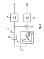
- Fig. 3 shows an example block diagram of the signal processing section 3 shown in Fig. 1 .
- 31 denotes a non-linear processing section that provides a dynamically non-linear dependency f1 from an amplitude characteristic of the input signal In input into the RF power amplifier circuit 10 shown in Fig. 1 .
- Which particular amplitude characteristic will be used depends on whether the input signal In is an RF signal with varying signal envelope, or whether according to another embodiment the signal In is a base band representation of the signal envelope of the RF signal to be generated by the power amplifier circuit 10, or whether the input signal In is a digital representation of the signal envelope to be to be generated by the RF power amplifier 10 according to yet another embodiment.
- 32 denotes a delay element to provide a delayed version InD of the amplitude characteristic of the input signal In to the RF power amplifier circuit as shown in Fig. 1 .
- 33 denotes a subtractor for subtracting the dynamically non-linearly processed input signal from the delayed version of the input signal In.
- the delayed version of the input signal and the output of the subtractor 33 are further processed in Up-Converters 34 and 35, respectively, in order to provide the RF signals to be amplified by the main amplifier deveice and auxiliary amplifier device, resp.
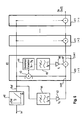
- Fig. 4 shows another example block diagram of the signal processing section 3 shown in Fig. 1 .
- the same reference numerals are used as in Fig. 3 to denote the same or corresponding parts, such that these parts need not be described again.
- 36 denotes an adder for adding a filtered version of the output from the dynamically non-linear processing section 31 to the delayed version InD of the amplitude characteristic of the input signal In.
- H12 and H22 denote filter circuits for cross coupling the branch signals in the main amplifier branch (Out1) and the auxiliary amplifier branch (Out2).
- the main amplifier signal branch includes a portion of the dynamic non-linear function.
- the filters H12 and H22 are designed such that the dynamic non-linear function cancels at the output of the RF power amplifier 10.
- the nonlinear signals of this invention are dynamic functions, which are by way of non-limiting example embodiments created by nonlinear filtering operations.
- the nonlinear filtering is carried out with respect to one or more boundaries.
- the boundaries can for example be constant amplitude limits or functions of the input signal amplitude or input signal level.
- the bandwidth-restricted nonlinear signals can in many cases be created and successfully applied without detailed knowledge of the output network's frequency dependences.
- a more optimal design may include the output network's frequency dependence.
- An additional filter at the input can be used to obtain a desired frequency response, for example one that gives maximum output power or maximal efficiency in the whole bandwidth, at the output node of the main amplifier.
- the nonlinear signal can be shaped independently using a single amplitude function as boundary. This translates into a cylindrical boundary in the 3-dimensional (complex signal as two dimensions plus the signal's amplitude as the third) space.
- the amplitude limit is constant, usually set to half the maximum output level.
- the resulting signal can be subtracted from a scaled version of the original signal, or a scaled version of the original signal can be subtracted from it.
- the signals that are input to the power transistors are made from combinations of scaled linear and nonlinear signals (made with the present method).
- the scaling can (suboptimally) be made frequency dependent, with generally different frequency dependencies for the different components and for the same component in the different combinations.
- Fig. 6 shows another example block diagram of a dynamic non-linear processing section for dynamic non-linear signal shaping.
- the peak (auxiliary) amplifier drive signal is built up from zero by successively adding filtered, rectified differences between the signal under construction and the desired (without bandwidth restrictions) nonlinear signal.
- Signal shaping for a Doherty amplifier with frequency dependence in the output network can thus be achieved with the structure shown in Fig. 6 , with the input signal optionally pre-filtered to achieve flat frequency response at the output node (by Z11/zo1, Z being Z-parameters of the output network and subscript o referring to output node).
- Another method for generating the dynamic nonlinear function of Doherty and similar amplifiers includes generating the optimal drive signals without bandwidth limitations.
- the overshooting parts (outside of boundaries) of bandwidth-limited versions of these signals are then extracted, recalculated into reinsertion signals, and filtered with the bandwidth-limiting filter in subsequent stages.
- the optimal direction for the reinsertion signal can be calculated. This works for moderate bandlimiting, since the filtered signals are close to the optimal ones.
- Yet another method is similar to the previous one, except that the optimal direction of reinsertion is assumed to be in the direction of the optimal drive signals without bandwidth limitations. This way, the derivatives do not have to be stored.
- the starting material is the drive signal that would give the highest efficiency without voltage limitations. Usually this means that a single transistor is driven.
- Fig. 7 shows an embodiment of a method of providing a power amplified radio frequency signal having a variable signal amplitude.
- the operations S12 and S22 relate to processing signals for the auxiliary amplifier branch 2 shown in Fig. 1 .
- the operations S11 and S21 relate to processing signals for the main amplifier 1 branch shown in Fig. 1 .
- the input signal In to the RF power amplifier 10 shown in Fig. 1 is processed to obtain the signal Out 1 for driving the main amplifier 1.
- the input signal In is processed with dynamic non-linearity to obtain the signal Out2 for driving the auxiliary amplifier 2.
- the main amplifier device and the auxiliary amplifier device are driven in accordance with the signals Out 1 and Out2, resp.
- the outputs of the main amplifier device and of the auxiliary amplifier device are combined together using the combiner network 4 shown in Fig. 1 in order to feed the combined output to a load ZL, as shown in S4.
- the invention allows operation with high efficiency, under restricted bandwidth conditions.
- the bandwidth expansion may be considerably reduced. Consequently, the invention also allows operation with increased signal bandwidth while retaining an acceptable efficiency.
Landscapes
- Engineering & Computer Science (AREA)
- Power Engineering (AREA)
- Amplifiers (AREA)
Applications Claiming Priority (2)
| Application Number | Priority Date | Filing Date | Title |
|---|---|---|---|
| US201161577741P | 2011-12-20 | 2011-12-20 | |
| PCT/EP2012/056429 WO2013091905A1 (en) | 2011-12-20 | 2012-04-10 | Radio frequency power amplifier circuit and method |
Publications (2)
| Publication Number | Publication Date |
|---|---|
| EP2748924A1 EP2748924A1 (en) | 2014-07-02 |
| EP2748924B1 true EP2748924B1 (en) | 2015-09-09 |
Family
ID=45954664
Family Applications (1)
| Application Number | Title | Priority Date | Filing Date |
|---|---|---|---|
| EP12714304.8A Not-in-force EP2748924B1 (en) | 2011-12-20 | 2012-04-10 | Radio frequency power amplifier circuit and method |
Country Status (4)
| Country | Link |
|---|---|
| US (1) | US8917141B2 (https=) |
| EP (1) | EP2748924B1 (https=) |
| IN (1) | IN2014CN03801A (https=) |
| WO (1) | WO2013091905A1 (https=) |
Families Citing this family (1)
| Publication number | Priority date | Publication date | Assignee | Title |
|---|---|---|---|---|
| US10181867B2 (en) * | 2015-10-08 | 2019-01-15 | Telefonaktiebolaget Lm Ericsson (Publ) | Crest factor reduction in a radio transmitter |
Family Cites Families (16)
| Publication number | Priority date | Publication date | Assignee | Title |
|---|---|---|---|---|
| SE516145C2 (sv) | 2000-06-06 | 2001-11-26 | Ericsson Telefon Ab L M | Sammansatt förstärkare |
| SE516847C2 (sv) * | 2000-07-07 | 2002-03-12 | Ericsson Telefon Ab L M | Sammansatt förstärkare samt sändare som innefattar en sådan förstärkare |
| SE516852C2 (sv) | 2000-07-07 | 2002-03-12 | Ericsson Telefon Ab L M | Sammansatt förstärkare, sändare med sådan förstärkare samt förfarande för att driva en dylik förstärkare resp. sändare |
| SE521268C2 (sv) | 2001-05-18 | 2003-10-14 | Ericsson Telefon Ab L M | Sammansatt förstärkare med optimerad linjäritet och effektivitet |
| SE521673C2 (sv) * | 2001-11-29 | 2003-11-25 | Ericsson Telefon Ab L M | Sammansatt förstärkare |
| US7260157B2 (en) * | 2002-11-21 | 2007-08-21 | Sotoudeh Hamedi Hagh | Phase shifted transmitter architecture for communication systems |
| US7038539B2 (en) * | 2003-05-06 | 2006-05-02 | Powerwave Technologies, Inc. | RF amplifier employing active load linearization |
| EP1758242A4 (en) | 2004-06-18 | 2008-04-09 | Mitsubishi Electric Corp | AMPLIFIER WITH HIGH EFFICIENCY |
| GB2418087B (en) | 2004-09-08 | 2008-03-19 | Filtronic Plc | A method and apparatus for pre-conditoning an electrical signal |
| US7711067B2 (en) | 2004-12-21 | 2010-05-04 | Telefonaktiebolaget L M Ericsson (Publ) | Bandwidth-constrained signal conditioning |
| DE602004029292D1 (de) | 2004-12-21 | 2010-11-04 | Ericsson Telefon Ab L M | Erzeugung von modulierten hochfrequenzsignalen |
| US7586428B2 (en) | 2005-02-25 | 2009-09-08 | Telefonaktiebolaget L M Ericsson (Publ) | Non-linear processing of signals |
| JP2007243491A (ja) * | 2006-03-07 | 2007-09-20 | R & K:Kk | 増幅回路 |
| US8165539B2 (en) | 2006-07-03 | 2012-04-24 | Telefonaktiebolaget L M Ericsson (Publ) | Apparatuses and a method for reducing peak power in telecommunications systems |
| US7961045B2 (en) * | 2007-03-30 | 2011-06-14 | Nortel Networks Limited | Amplifier pre-distortion systems and methods |
| US8848824B2 (en) * | 2008-03-07 | 2014-09-30 | Andrew M. Teetzel | High efficiency RF system linearizer using controlled complex nonlinear distortion generators |
-
2012
- 2012-04-10 IN IN3801CHN2014 patent/IN2014CN03801A/en unknown
- 2012-04-10 US US13/505,777 patent/US8917141B2/en active Active
- 2012-04-10 WO PCT/EP2012/056429 patent/WO2013091905A1/en not_active Ceased
- 2012-04-10 EP EP12714304.8A patent/EP2748924B1/en not_active Not-in-force
Also Published As
| Publication number | Publication date |
|---|---|
| US8917141B2 (en) | 2014-12-23 |
| EP2748924A1 (en) | 2014-07-02 |
| IN2014CN03801A (https=) | 2015-10-16 |
| WO2013091905A1 (en) | 2013-06-27 |
| US20140320213A1 (en) | 2014-10-30 |
Similar Documents
| Publication | Publication Date | Title |
|---|---|---|
| KR101767297B1 (ko) | 포락선 추적을 위한 장치 및 방법 | |
| KR100749899B1 (ko) | 전력 증폭기 | |
| JP5614273B2 (ja) | 増幅装置 | |
| KR102890918B1 (ko) | 가변 전력 증폭기 바이어스 임피던스 | |
| US20230020495A1 (en) | Load-modulated push-pull power amplifier | |
| WO2002005421A1 (en) | Transmitter including a composite amplifier | |
| EP3205015B1 (en) | Amplifier circuit and method | |
| JP2009260658A (ja) | 電力増幅器 | |
| US9590564B2 (en) | Multiband power amplification apparatus | |
| WO2013176147A1 (ja) | 電力増幅回路 | |
| WO2016182485A1 (en) | Composite power amplifier | |
| JP4784558B2 (ja) | 電力増幅装置およびこれを用いた無線通信装置 | |
| WO2015133003A1 (ja) | 送信機、送信方法 | |
| JP2015220680A (ja) | 高効率増幅器 | |
| EP2748924B1 (en) | Radio frequency power amplifier circuit and method | |
| JP2009284174A (ja) | 送信回路、電力制御方法およびコンピュータプログラム | |
| CN112019167A (zh) | 放大装置和方法 | |
| JP4825495B2 (ja) | 歪制御機能付き増幅装置 | |
| KR101477715B1 (ko) | 클래스 e 전력증폭기의 효율 및 이득 향상을 위한 다중모드 동적 바이어싱 시스템 및 그 방법 | |
| JP4722384B2 (ja) | 多段高出力増幅器 | |
| KR100774385B1 (ko) | 전력 증폭기 | |
| US20240396501A1 (en) | Distributed power amplifier | |
| WO2012163875A1 (en) | Envelope path processing for envelope tracking amplification stage | |
| JP2008277908A (ja) | デジタルプレディストータ | |
| HK1190834B (en) | Apparatus and methods for envelope tracking |
Legal Events
| Date | Code | Title | Description |
|---|---|---|---|
| PUAI | Public reference made under article 153(3) epc to a published international application that has entered the european phase |
Free format text: ORIGINAL CODE: 0009012 |
|
| 17P | Request for examination filed |
Effective date: 20140325 |
|
| AK | Designated contracting states |
Kind code of ref document: A1 Designated state(s): AL AT BE BG CH CY CZ DE DK EE ES FI FR GB GR HR HU IE IS IT LI LT LU LV MC MK MT NL NO PL PT RO RS SE SI SK SM TR |
|
| RIN1 | Information on inventor provided before grant (corrected) |
Inventor name: KLINGBERG, MATS Inventor name: HELLBERG, RICHARD Inventor name: FONDEN, TONY |
|
| DAX | Request for extension of the european patent (deleted) | ||
| GRAP | Despatch of communication of intention to grant a patent |
Free format text: ORIGINAL CODE: EPIDOSNIGR1 |
|
| RIC1 | Information provided on ipc code assigned before grant |
Ipc: H03F 1/02 20060101AFI20150422BHEP Ipc: H03F 3/21 20060101ALI20150422BHEP Ipc: H03F 3/193 20060101ALI20150422BHEP |
|
| INTG | Intention to grant announced |
Effective date: 20150513 |
|
| GRAS | Grant fee paid |
Free format text: ORIGINAL CODE: EPIDOSNIGR3 |
|
| GRAA | (expected) grant |
Free format text: ORIGINAL CODE: 0009210 |
|
| AK | Designated contracting states |
Kind code of ref document: B1 Designated state(s): AL AT BE BG CH CY CZ DE DK EE ES FI FR GB GR HR HU IE IS IT LI LT LU LV MC MK MT NL NO PL PT RO RS SE SI SK SM TR |
|
| REG | Reference to a national code |
Ref country code: GB Ref legal event code: FG4D |
|
| REG | Reference to a national code |
Ref country code: AT Ref legal event code: REF Ref document number: 748855 Country of ref document: AT Kind code of ref document: T Effective date: 20150915 Ref country code: CH Ref legal event code: EP |
|
| REG | Reference to a national code |
Ref country code: IE Ref legal event code: FG4D |
|
| REG | Reference to a national code |
Ref country code: DE Ref legal event code: R096 Ref document number: 602012010314 Country of ref document: DE |
|
| PG25 | Lapsed in a contracting state [announced via postgrant information from national office to epo] |
Ref country code: GR Free format text: LAPSE BECAUSE OF FAILURE TO SUBMIT A TRANSLATION OF THE DESCRIPTION OR TO PAY THE FEE WITHIN THE PRESCRIBED TIME-LIMIT Effective date: 20151210 Ref country code: LT Free format text: LAPSE BECAUSE OF FAILURE TO SUBMIT A TRANSLATION OF THE DESCRIPTION OR TO PAY THE FEE WITHIN THE PRESCRIBED TIME-LIMIT Effective date: 20150909 Ref country code: FI Free format text: LAPSE BECAUSE OF FAILURE TO SUBMIT A TRANSLATION OF THE DESCRIPTION OR TO PAY THE FEE WITHIN THE PRESCRIBED TIME-LIMIT Effective date: 20150909 Ref country code: LV Free format text: LAPSE BECAUSE OF FAILURE TO SUBMIT A TRANSLATION OF THE DESCRIPTION OR TO PAY THE FEE WITHIN THE PRESCRIBED TIME-LIMIT Effective date: 20150909 Ref country code: NO Free format text: LAPSE BECAUSE OF FAILURE TO SUBMIT A TRANSLATION OF THE DESCRIPTION OR TO PAY THE FEE WITHIN THE PRESCRIBED TIME-LIMIT Effective date: 20151209 |
|
| REG | Reference to a national code |
Ref country code: LT Ref legal event code: MG4D Ref country code: NL Ref legal event code: FP |
|
| REG | Reference to a national code |
Ref country code: AT Ref legal event code: MK05 Ref document number: 748855 Country of ref document: AT Kind code of ref document: T Effective date: 20150909 |
|
| PG25 | Lapsed in a contracting state [announced via postgrant information from national office to epo] |
Ref country code: HR Free format text: LAPSE BECAUSE OF FAILURE TO SUBMIT A TRANSLATION OF THE DESCRIPTION OR TO PAY THE FEE WITHIN THE PRESCRIBED TIME-LIMIT Effective date: 20150909 Ref country code: RS Free format text: LAPSE BECAUSE OF FAILURE TO SUBMIT A TRANSLATION OF THE DESCRIPTION OR TO PAY THE FEE WITHIN THE PRESCRIBED TIME-LIMIT Effective date: 20150909 Ref country code: SE Free format text: LAPSE BECAUSE OF FAILURE TO SUBMIT A TRANSLATION OF THE DESCRIPTION OR TO PAY THE FEE WITHIN THE PRESCRIBED TIME-LIMIT Effective date: 20150909 Ref country code: ES Free format text: LAPSE BECAUSE OF FAILURE TO SUBMIT A TRANSLATION OF THE DESCRIPTION OR TO PAY THE FEE WITHIN THE PRESCRIBED TIME-LIMIT Effective date: 20150909 |
|
| PG25 | Lapsed in a contracting state [announced via postgrant information from national office to epo] |
Ref country code: CZ Free format text: LAPSE BECAUSE OF FAILURE TO SUBMIT A TRANSLATION OF THE DESCRIPTION OR TO PAY THE FEE WITHIN THE PRESCRIBED TIME-LIMIT Effective date: 20150909 Ref country code: EE Free format text: LAPSE BECAUSE OF FAILURE TO SUBMIT A TRANSLATION OF THE DESCRIPTION OR TO PAY THE FEE WITHIN THE PRESCRIBED TIME-LIMIT Effective date: 20150909 Ref country code: IS Free format text: LAPSE BECAUSE OF FAILURE TO SUBMIT A TRANSLATION OF THE DESCRIPTION OR TO PAY THE FEE WITHIN THE PRESCRIBED TIME-LIMIT Effective date: 20160109 Ref country code: IT Free format text: LAPSE BECAUSE OF FAILURE TO SUBMIT A TRANSLATION OF THE DESCRIPTION OR TO PAY THE FEE WITHIN THE PRESCRIBED TIME-LIMIT Effective date: 20150909 Ref country code: SK Free format text: LAPSE BECAUSE OF FAILURE TO SUBMIT A TRANSLATION OF THE DESCRIPTION OR TO PAY THE FEE WITHIN THE PRESCRIBED TIME-LIMIT Effective date: 20150909 |
|
| PG25 | Lapsed in a contracting state [announced via postgrant information from national office to epo] |
Ref country code: PT Free format text: LAPSE BECAUSE OF FAILURE TO SUBMIT A TRANSLATION OF THE DESCRIPTION OR TO PAY THE FEE WITHIN THE PRESCRIBED TIME-LIMIT Effective date: 20160111 Ref country code: PL Free format text: LAPSE BECAUSE OF FAILURE TO SUBMIT A TRANSLATION OF THE DESCRIPTION OR TO PAY THE FEE WITHIN THE PRESCRIBED TIME-LIMIT Effective date: 20150909 Ref country code: AT Free format text: LAPSE BECAUSE OF FAILURE TO SUBMIT A TRANSLATION OF THE DESCRIPTION OR TO PAY THE FEE WITHIN THE PRESCRIBED TIME-LIMIT Effective date: 20150909 Ref country code: RO Free format text: LAPSE BECAUSE OF FAILURE TO SUBMIT A TRANSLATION OF THE DESCRIPTION OR TO PAY THE FEE WITHIN THE PRESCRIBED TIME-LIMIT Effective date: 20150909 |
|
| REG | Reference to a national code |
Ref country code: DE Ref legal event code: R097 Ref document number: 602012010314 Country of ref document: DE |
|
| PLBE | No opposition filed within time limit |
Free format text: ORIGINAL CODE: 0009261 |
|
| STAA | Information on the status of an ep patent application or granted ep patent |
Free format text: STATUS: NO OPPOSITION FILED WITHIN TIME LIMIT |
|
| 26N | No opposition filed |
Effective date: 20160610 |
|
| PG25 | Lapsed in a contracting state [announced via postgrant information from national office to epo] |
Ref country code: SI Free format text: LAPSE BECAUSE OF FAILURE TO SUBMIT A TRANSLATION OF THE DESCRIPTION OR TO PAY THE FEE WITHIN THE PRESCRIBED TIME-LIMIT Effective date: 20150909 Ref country code: DK Free format text: LAPSE BECAUSE OF FAILURE TO SUBMIT A TRANSLATION OF THE DESCRIPTION OR TO PAY THE FEE WITHIN THE PRESCRIBED TIME-LIMIT Effective date: 20150909 Ref country code: BE Free format text: LAPSE BECAUSE OF NON-PAYMENT OF DUE FEES Effective date: 20160430 |
|
| REG | Reference to a national code |
Ref country code: CH Ref legal event code: PL |
|
| PG25 | Lapsed in a contracting state [announced via postgrant information from national office to epo] |
Ref country code: BE Free format text: LAPSE BECAUSE OF FAILURE TO SUBMIT A TRANSLATION OF THE DESCRIPTION OR TO PAY THE FEE WITHIN THE PRESCRIBED TIME-LIMIT Effective date: 20150909 Ref country code: LU Free format text: LAPSE BECAUSE OF FAILURE TO SUBMIT A TRANSLATION OF THE DESCRIPTION OR TO PAY THE FEE WITHIN THE PRESCRIBED TIME-LIMIT Effective date: 20160410 |
|
| REG | Reference to a national code |
Ref country code: IE Ref legal event code: MM4A |
|
| REG | Reference to a national code |
Ref country code: FR Ref legal event code: ST Effective date: 20161230 |
|
| PG25 | Lapsed in a contracting state [announced via postgrant information from national office to epo] |
Ref country code: CH Free format text: LAPSE BECAUSE OF NON-PAYMENT OF DUE FEES Effective date: 20160430 Ref country code: LI Free format text: LAPSE BECAUSE OF NON-PAYMENT OF DUE FEES Effective date: 20160430 Ref country code: FR Free format text: LAPSE BECAUSE OF NON-PAYMENT OF DUE FEES Effective date: 20160502 |
|
| PG25 | Lapsed in a contracting state [announced via postgrant information from national office to epo] |
Ref country code: IE Free format text: LAPSE BECAUSE OF NON-PAYMENT OF DUE FEES Effective date: 20160410 |
|
| PG25 | Lapsed in a contracting state [announced via postgrant information from national office to epo] |
Ref country code: HU Free format text: LAPSE BECAUSE OF FAILURE TO SUBMIT A TRANSLATION OF THE DESCRIPTION OR TO PAY THE FEE WITHIN THE PRESCRIBED TIME-LIMIT; INVALID AB INITIO Effective date: 20120410 Ref country code: SM Free format text: LAPSE BECAUSE OF FAILURE TO SUBMIT A TRANSLATION OF THE DESCRIPTION OR TO PAY THE FEE WITHIN THE PRESCRIBED TIME-LIMIT Effective date: 20150909 |
|
| PG25 | Lapsed in a contracting state [announced via postgrant information from national office to epo] |
Ref country code: MT Free format text: LAPSE BECAUSE OF NON-PAYMENT OF DUE FEES Effective date: 20160430 Ref country code: MC Free format text: LAPSE BECAUSE OF FAILURE TO SUBMIT A TRANSLATION OF THE DESCRIPTION OR TO PAY THE FEE WITHIN THE PRESCRIBED TIME-LIMIT Effective date: 20150909 Ref country code: CY Free format text: LAPSE BECAUSE OF FAILURE TO SUBMIT A TRANSLATION OF THE DESCRIPTION OR TO PAY THE FEE WITHIN THE PRESCRIBED TIME-LIMIT Effective date: 20150909 Ref country code: MK Free format text: LAPSE BECAUSE OF FAILURE TO SUBMIT A TRANSLATION OF THE DESCRIPTION OR TO PAY THE FEE WITHIN THE PRESCRIBED TIME-LIMIT Effective date: 20150909 |
|
| PG25 | Lapsed in a contracting state [announced via postgrant information from national office to epo] |
Ref country code: BG Free format text: LAPSE BECAUSE OF FAILURE TO SUBMIT A TRANSLATION OF THE DESCRIPTION OR TO PAY THE FEE WITHIN THE PRESCRIBED TIME-LIMIT Effective date: 20150909 |
|
| PG25 | Lapsed in a contracting state [announced via postgrant information from national office to epo] |
Ref country code: AL Free format text: LAPSE BECAUSE OF FAILURE TO SUBMIT A TRANSLATION OF THE DESCRIPTION OR TO PAY THE FEE WITHIN THE PRESCRIBED TIME-LIMIT Effective date: 20150909 Ref country code: TR Free format text: LAPSE BECAUSE OF FAILURE TO SUBMIT A TRANSLATION OF THE DESCRIPTION OR TO PAY THE FEE WITHIN THE PRESCRIBED TIME-LIMIT Effective date: 20150909 |
|
| PGFP | Annual fee paid to national office [announced via postgrant information from national office to epo] |
Ref country code: NL Payment date: 20220426 Year of fee payment: 11 |
|
| PGFP | Annual fee paid to national office [announced via postgrant information from national office to epo] |
Ref country code: GB Payment date: 20220427 Year of fee payment: 11 Ref country code: DE Payment date: 20220427 Year of fee payment: 11 |
|
| REG | Reference to a national code |
Ref country code: DE Ref legal event code: R119 Ref document number: 602012010314 Country of ref document: DE |
|
| REG | Reference to a national code |
Ref country code: NL Ref legal event code: MM Effective date: 20230501 |
|
| GBPC | Gb: european patent ceased through non-payment of renewal fee |
Effective date: 20230410 |
|
| PG25 | Lapsed in a contracting state [announced via postgrant information from national office to epo] |
Ref country code: GB Free format text: LAPSE BECAUSE OF NON-PAYMENT OF DUE FEES Effective date: 20230410 |
|
| PG25 | Lapsed in a contracting state [announced via postgrant information from national office to epo] |
Ref country code: NL Free format text: LAPSE BECAUSE OF NON-PAYMENT OF DUE FEES Effective date: 20230501 Ref country code: GB Free format text: LAPSE BECAUSE OF NON-PAYMENT OF DUE FEES Effective date: 20230410 Ref country code: DE Free format text: LAPSE BECAUSE OF NON-PAYMENT OF DUE FEES Effective date: 20231103 |