EP2743762A1 - Liquid crystal display device - Google Patents
Liquid crystal display device Download PDFInfo
- Publication number
- EP2743762A1 EP2743762A1 EP20130192070 EP13192070A EP2743762A1 EP 2743762 A1 EP2743762 A1 EP 2743762A1 EP 20130192070 EP20130192070 EP 20130192070 EP 13192070 A EP13192070 A EP 13192070A EP 2743762 A1 EP2743762 A1 EP 2743762A1
- Authority
- EP
- European Patent Office
- Prior art keywords
- layer
- liquid crystal
- lines
- crystal panel
- line
- Prior art date
- Legal status (The legal status is an assumption and is not a legal conclusion. Google has not performed a legal analysis and makes no representation as to the accuracy of the status listed.)
- Granted
Links
Images





Classifications
-
- G—PHYSICS
- G02—OPTICS
- G02F—OPTICAL DEVICES OR ARRANGEMENTS FOR THE CONTROL OF LIGHT BY MODIFICATION OF THE OPTICAL PROPERTIES OF THE MEDIA OF THE ELEMENTS INVOLVED THEREIN; NON-LINEAR OPTICS; FREQUENCY-CHANGING OF LIGHT; OPTICAL LOGIC ELEMENTS; OPTICAL ANALOGUE/DIGITAL CONVERTERS
- G02F1/00—Devices or arrangements for the control of the intensity, colour, phase, polarisation or direction of light arriving from an independent light source, e.g. switching, gating or modulating; Non-linear optics
- G02F1/01—Devices or arrangements for the control of the intensity, colour, phase, polarisation or direction of light arriving from an independent light source, e.g. switching, gating or modulating; Non-linear optics for the control of the intensity, phase, polarisation or colour
- G02F1/13—Devices or arrangements for the control of the intensity, colour, phase, polarisation or direction of light arriving from an independent light source, e.g. switching, gating or modulating; Non-linear optics for the control of the intensity, phase, polarisation or colour based on liquid crystals, e.g. single liquid crystal display cells
- G02F1/133—Constructional arrangements; Operation of liquid crystal cells; Circuit arrangements
- G02F1/13306—Circuit arrangements or driving methods for the control of single liquid crystal cells
-
- G—PHYSICS
- G02—OPTICS
- G02F—OPTICAL DEVICES OR ARRANGEMENTS FOR THE CONTROL OF LIGHT BY MODIFICATION OF THE OPTICAL PROPERTIES OF THE MEDIA OF THE ELEMENTS INVOLVED THEREIN; NON-LINEAR OPTICS; FREQUENCY-CHANGING OF LIGHT; OPTICAL LOGIC ELEMENTS; OPTICAL ANALOGUE/DIGITAL CONVERTERS
- G02F1/00—Devices or arrangements for the control of the intensity, colour, phase, polarisation or direction of light arriving from an independent light source, e.g. switching, gating or modulating; Non-linear optics
- G02F1/01—Devices or arrangements for the control of the intensity, colour, phase, polarisation or direction of light arriving from an independent light source, e.g. switching, gating or modulating; Non-linear optics for the control of the intensity, phase, polarisation or colour
- G02F1/13—Devices or arrangements for the control of the intensity, colour, phase, polarisation or direction of light arriving from an independent light source, e.g. switching, gating or modulating; Non-linear optics for the control of the intensity, phase, polarisation or colour based on liquid crystals, e.g. single liquid crystal display cells
- G02F1/133—Constructional arrangements; Operation of liquid crystal cells; Circuit arrangements
- G02F1/1333—Constructional arrangements; Manufacturing methods
- G02F1/1343—Electrodes
- G02F1/134309—Electrodes characterised by their geometrical arrangement
- G02F1/134363—Electrodes characterised by their geometrical arrangement for applying an electric field parallel to the substrate, i.e. in-plane switching [IPS]
-
- G—PHYSICS
- G02—OPTICS
- G02F—OPTICAL DEVICES OR ARRANGEMENTS FOR THE CONTROL OF LIGHT BY MODIFICATION OF THE OPTICAL PROPERTIES OF THE MEDIA OF THE ELEMENTS INVOLVED THEREIN; NON-LINEAR OPTICS; FREQUENCY-CHANGING OF LIGHT; OPTICAL LOGIC ELEMENTS; OPTICAL ANALOGUE/DIGITAL CONVERTERS
- G02F1/00—Devices or arrangements for the control of the intensity, colour, phase, polarisation or direction of light arriving from an independent light source, e.g. switching, gating or modulating; Non-linear optics
- G02F1/01—Devices or arrangements for the control of the intensity, colour, phase, polarisation or direction of light arriving from an independent light source, e.g. switching, gating or modulating; Non-linear optics for the control of the intensity, phase, polarisation or colour
- G02F1/13—Devices or arrangements for the control of the intensity, colour, phase, polarisation or direction of light arriving from an independent light source, e.g. switching, gating or modulating; Non-linear optics for the control of the intensity, phase, polarisation or colour based on liquid crystals, e.g. single liquid crystal display cells
- G02F1/133—Constructional arrangements; Operation of liquid crystal cells; Circuit arrangements
-
- G—PHYSICS
- G02—OPTICS
- G02F—OPTICAL DEVICES OR ARRANGEMENTS FOR THE CONTROL OF LIGHT BY MODIFICATION OF THE OPTICAL PROPERTIES OF THE MEDIA OF THE ELEMENTS INVOLVED THEREIN; NON-LINEAR OPTICS; FREQUENCY-CHANGING OF LIGHT; OPTICAL LOGIC ELEMENTS; OPTICAL ANALOGUE/DIGITAL CONVERTERS
- G02F1/00—Devices or arrangements for the control of the intensity, colour, phase, polarisation or direction of light arriving from an independent light source, e.g. switching, gating or modulating; Non-linear optics
- G02F1/01—Devices or arrangements for the control of the intensity, colour, phase, polarisation or direction of light arriving from an independent light source, e.g. switching, gating or modulating; Non-linear optics for the control of the intensity, phase, polarisation or colour
- G02F1/13—Devices or arrangements for the control of the intensity, colour, phase, polarisation or direction of light arriving from an independent light source, e.g. switching, gating or modulating; Non-linear optics for the control of the intensity, phase, polarisation or colour based on liquid crystals, e.g. single liquid crystal display cells
- G02F1/133—Constructional arrangements; Operation of liquid crystal cells; Circuit arrangements
- G02F1/1333—Constructional arrangements; Manufacturing methods
- G02F1/1345—Conductors connecting electrodes to cell terminals
-
- G—PHYSICS
- G02—OPTICS
- G02F—OPTICAL DEVICES OR ARRANGEMENTS FOR THE CONTROL OF LIGHT BY MODIFICATION OF THE OPTICAL PROPERTIES OF THE MEDIA OF THE ELEMENTS INVOLVED THEREIN; NON-LINEAR OPTICS; FREQUENCY-CHANGING OF LIGHT; OPTICAL LOGIC ELEMENTS; OPTICAL ANALOGUE/DIGITAL CONVERTERS
- G02F1/00—Devices or arrangements for the control of the intensity, colour, phase, polarisation or direction of light arriving from an independent light source, e.g. switching, gating or modulating; Non-linear optics
- G02F1/01—Devices or arrangements for the control of the intensity, colour, phase, polarisation or direction of light arriving from an independent light source, e.g. switching, gating or modulating; Non-linear optics for the control of the intensity, phase, polarisation or colour
- G02F1/13—Devices or arrangements for the control of the intensity, colour, phase, polarisation or direction of light arriving from an independent light source, e.g. switching, gating or modulating; Non-linear optics for the control of the intensity, phase, polarisation or colour based on liquid crystals, e.g. single liquid crystal display cells
- G02F1/133—Constructional arrangements; Operation of liquid crystal cells; Circuit arrangements
- G02F1/136—Liquid crystal cells structurally associated with a semi-conducting layer or substrate, e.g. cells forming part of an integrated circuit
- G02F1/1362—Active matrix addressed cells
- G02F1/136286—Wiring, e.g. gate line, drain line
-
- G—PHYSICS
- G02—OPTICS
- G02F—OPTICAL DEVICES OR ARRANGEMENTS FOR THE CONTROL OF LIGHT BY MODIFICATION OF THE OPTICAL PROPERTIES OF THE MEDIA OF THE ELEMENTS INVOLVED THEREIN; NON-LINEAR OPTICS; FREQUENCY-CHANGING OF LIGHT; OPTICAL LOGIC ELEMENTS; OPTICAL ANALOGUE/DIGITAL CONVERTERS
- G02F1/00—Devices or arrangements for the control of the intensity, colour, phase, polarisation or direction of light arriving from an independent light source, e.g. switching, gating or modulating; Non-linear optics
- G02F1/01—Devices or arrangements for the control of the intensity, colour, phase, polarisation or direction of light arriving from an independent light source, e.g. switching, gating or modulating; Non-linear optics for the control of the intensity, phase, polarisation or colour
- G02F1/13—Devices or arrangements for the control of the intensity, colour, phase, polarisation or direction of light arriving from an independent light source, e.g. switching, gating or modulating; Non-linear optics for the control of the intensity, phase, polarisation or colour based on liquid crystals, e.g. single liquid crystal display cells
- G02F1/133—Constructional arrangements; Operation of liquid crystal cells; Circuit arrangements
- G02F1/1333—Constructional arrangements; Manufacturing methods
- G02F1/1345—Conductors connecting electrodes to cell terminals
- G02F1/13456—Cell terminals located on one side of the display only
-
- G—PHYSICS
- G02—OPTICS
- G02F—OPTICAL DEVICES OR ARRANGEMENTS FOR THE CONTROL OF LIGHT BY MODIFICATION OF THE OPTICAL PROPERTIES OF THE MEDIA OF THE ELEMENTS INVOLVED THEREIN; NON-LINEAR OPTICS; FREQUENCY-CHANGING OF LIGHT; OPTICAL LOGIC ELEMENTS; OPTICAL ANALOGUE/DIGITAL CONVERTERS
- G02F1/00—Devices or arrangements for the control of the intensity, colour, phase, polarisation or direction of light arriving from an independent light source, e.g. switching, gating or modulating; Non-linear optics
- G02F1/01—Devices or arrangements for the control of the intensity, colour, phase, polarisation or direction of light arriving from an independent light source, e.g. switching, gating or modulating; Non-linear optics for the control of the intensity, phase, polarisation or colour
- G02F1/13—Devices or arrangements for the control of the intensity, colour, phase, polarisation or direction of light arriving from an independent light source, e.g. switching, gating or modulating; Non-linear optics for the control of the intensity, phase, polarisation or colour based on liquid crystals, e.g. single liquid crystal display cells
- G02F1/133—Constructional arrangements; Operation of liquid crystal cells; Circuit arrangements
- G02F1/136—Liquid crystal cells structurally associated with a semi-conducting layer or substrate, e.g. cells forming part of an integrated circuit
- G02F1/1362—Active matrix addressed cells
- G02F1/136286—Wiring, e.g. gate line, drain line
- G02F1/13629—Multilayer wirings
-
- G—PHYSICS
- G09—EDUCATION; CRYPTOGRAPHY; DISPLAY; ADVERTISING; SEALS
- G09G—ARRANGEMENTS OR CIRCUITS FOR CONTROL OF INDICATING DEVICES USING STATIC MEANS TO PRESENT VARIABLE INFORMATION
- G09G2310/00—Command of the display device
- G09G2310/02—Addressing, scanning or driving the display screen or processing steps related thereto
- G09G2310/0264—Details of driving circuits
- G09G2310/0281—Arrangement of scan or data electrode driver circuits at the periphery of a panel not inherent to a split matrix structure
Definitions
- the present invention relates to a flat panel display device, and more particularly, to a liquid crystal display (LCD) device with a reduced bezel size and an enhanced aesthetic design appearance.
- LCD liquid crystal display
- LCD liquid crystal display
- PDP plasma display panels
- FED field emission display
- OLED organic light emitting diode
- the LCD devices are being continuously expanded in application field because the LCD devices are easily manufactured due to the advance of manufacturing technology and realize drivability of a driver, low power consumption, a high-quality image, and a large screen.
- FIG. 1 is a view schematically illustrating a related art LCD device
- FIG. 2 is a view schematically illustrating a pixel structure of the related art LCD device.
- the related art LCD device a liquid crystal panel in which a plurality of pixels are arranged in a matrix type, a driving circuit unit that drives the liquid crystal panel, a backlight unit (not shown) that supplies light to the liquid crystal panel, and a bezel (not shown) that is formed to surround the liquid crystal panel and the driving circuit unit.
- the liquid crystal panel includes a lower substrate (TFT array substrate) in which the plurality of pixels and a plurality of lines for driving the pixels are provided, an upper substrate (color filter array substrate) in which a plurality of color filters and a plurality of black matrixes are formed, and a liquid crystal layer disposed between the two substrates.
- TFT array substrate TFT array substrate
- color filter array substrate color filter array substrate
- a plurality of gate lines and a plurality of data lines are formed to intersect each other in the lower substrate of the liquid crystal panel, and the plurality of pixels are respectively formed in a plurality of areas in which the gate lines and the data lines intersect each other.
- a thin film transistor (TFT), a switching element, is formed in each of the pixels, and a pixel electrode and a common electrode for applying an electric field are formed in each of the pixels.
- the liquid crystal panel includes a display area 10 that displays an image and a non-display area that cannot display an image.
- a data driver 40 is connected to an upper non-display area of the liquid crystal panel.
- a pad area in which a plurality of pads receiving external signals for driving the respective pixels are provided, is formed in an outer non-display area of the lower substrate of the liquid crystal panel, and a link line that links a corresponding pad to a corresponding TFT and electrode is formed in plurality.
- FIG. 3 is a sectional view illustrating the non-display area of the liquid crystal panel of the related art.
- a seal 30 is formed in an outer portion (i.e., non-display area) of an active area in which the plurality of pixels are formed, and the upper substrate 1 and the lower substrate 2 are coupled to each other with the seal 30.
- a gate-in panel (GIP) type in which a built-in shift register is disposed in the lower substrate 2, is applied for reducing the manufacturing cost of the LCD device due to the driving circuit unit adhered to the liquid crystal panel and reducing a volume and a weight.
- GIP gate-in panel
- the gate driver and the data driver receive different driving signals from a timing controller mounted on a printed circuit board (PCB) 50 and receive a driving voltage supplied from a power supply to thereby be driven.
- PCB printed circuit board
- the GIP type gate driver is disposed in each of the left and right non-display areas of the lower substrate 2. In FIG. 3 , only the gate driver disposed at a left side of the lower substrate 2 is illustrated.
- the GIP type gate driver includes a common voltage link area 22 receiving a common voltage (Vcom), a ground (GND) link area 24, and a shift register logic area 26 that generates a scan signal for turning on the TFTs of the liquid crystal panel.
- the manufacturing cost of the LCD device can be reduced by applying the GIP type gate driver, and a volume and a weight can be reduced.
- bezel sizes of the left and right sides of the liquid crystal panel increase.
- the ground link area 24 overlaps the seal 30, for increasing a bezel size.
- the common voltage link area 22 is formed to have a width of about 1mm
- the shift register logic area 26 of the GIP type gate driver is formed to have a width of 5 mm to 6 mm.
- a left bezel width and a right bezel width are formed at 7 mm to 8 mm, and thus, there is a limitation in reducing a size, causing a reduction in an aesthetic design appearance.
- a structure was proposed in which the TFT array substrate and the color filter array substrate are switched in disposed position, and the TFT array substrate is disposed at an upper side.
- external light is reflected by a plurality of lines formed in the TFT array substrate, causing a reduction in visibility of an image.
- the present invention is directed to provide a flat panel display device that substantially obviates one or more problems due to limitations and disadvantages of the related art.
- An aspect of the present invention is directed to provide an LCD device with a reduced size of a bezel formed at an outer portion of a liquid crystal panel.
- Another aspect of the present invention is directed to provide an LCD device with a good aesthetic design appearance.
- Another aspect of the present invention is directed to provide an LCD device with a reduced size of a pad area.
- Another aspect of the present invention is directed to provide an LCD device of which the manufacturing cost is reduced.
- an LCD device including: a plurality of first gate lines and a plurality of data lines vertically formed in a liquid crystal panel; a plurality of second gate lines horizontally formed in the liquid crystal panel, the plurality of second gate lines and the plurality of first gate lines being formed on different layers; and a plurality of driving ICs disposed in an upper or lower non-display area of the liquid crystal panel, connected to the plurality of first gate lines to supply a scan signal, and connected to the plurality of data lines to supply data voltages, wherein, the plurality of first gate lines and the plurality of second gate lines are electrically connected to each other in pairs through a contact in an overlapping area therebetween, and the plurality of first gate lines and the plurality of data lines are formed on different layers.
- FIG. 1 is a view schematically illustrating a related art LCD device
- FIG. 2 is a view schematically illustrating a pixel structure of the related art LCD device
- FIG. 3 is a sectional view illustrating a non-display area of a related art liquid crystal panel
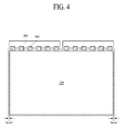
- FIG. 4 is a view schematically illustrating an LCD device according to an embodiment of the present invention.
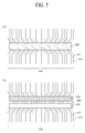
- FIG. 5 is views illustrating a driving IC of the LCD device according to an embodiment of the present invention.
- FIG. 6 is a view illustrating a pixel structure of an LCD device according to a first embodiment of the present invention.
- FIG. 7 is views for describing a left bezel size and right bezel size of the LCD device according to an embodiment of the present invention.
- FIG. 8 is a view specifically illustrating the pixel structure of the LCD device according to the first embodiment of the present invention.
- FIG. 9 is a sectional view taken along A1-A2 line of FIG. 8 ;
- FIG. 10 is a view specifically illustrating a pixel structure of an LCD device according to a second embodiment of the present invention.
- FIG. 11 is a sectional view taken along B1-B2 line of FIG. 10 , and is a view illustrating an opening area of each pixel being enlarged;
- FIG. 12 is a view illustrating a parasitic capacitance being generated between a vertical gate line and a common electrode, in the pixel structure according to the first embodiment of the present invention
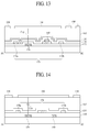
- FIG. 13 is a sectional view illustrating a pixel structure of an LCD device according to a third embodiment of the present invention.
- FIG. 14 is a sectional view illustrating a pixel structure of an LCD device according to a fourth embodiment of the present invention.
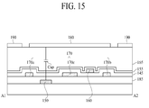
- FIG. 15 is a sectional view illustrating a pixel structure of an LCD device according to a fifth embodiment of the present invention.
- FIG. 16 is a view illustrating a liquid crystal panel being long provided in a vertical direction, in another embodiment of the present invention.
- At least one should be understood as including any and all combinations of one or more of the associated listed items.
- the meaning of "at least one of a first item, a second item, and a third item” denotes the combination of all items proposed from two or more of the first item, the second item, and the third item as well as the first item, the second item, or the third item.
- a structure for example, an electrode, a line, a wiring, a layer, or a contact
- this description should be construed as including a case where the structures contact each other and moreover a case where a third structure is disposed therebetween.
- LCD devices have been variously developed in a twisted nematic (TN) mode, a vertical alignment (VA) mode, an in-plane switching (IPS) mode, and a fringe field switching (FFS) mode according to a scheme of adjusting the alignment of liquid crystal.
- TN twisted nematic
- VA vertical alignment
- IPS in-plane switching
- FFS fringe field switching
- the IPS mode and the FFS mode are modes in which a plurality of pixel electrodes and a common electrode are arranged on a lower substrate, thereby adjusting the alignment of liquid crystal with electric fields between the pixel electrodes and the common electrode.
- An LCD device according to an embodiment of the present invention may be applied irrespective of modes, but the IPS mode will be described as an example.
- the main contents of the present invention are to reduce a bezel size of an LCD device. Therefore, an instrument irrelevant to a bezel and a backlight unit supplying light to a liquid crystal panel may not be illustrated, and their detailed description may not be provided.
- FIG. 4 is a view schematically illustrating an LCD device according to an embodiment of the present invention.
- the LCD device includes a liquid crystal panel 100 in which a plurality of pixels are arranged in a matrix type, a plurality of driving ICs 400 for driving the liquid crystal panel 100, a printed circuit board (PCB) 300 on which a control unit supplying a control signal for driving the plurality of driving ICs 400 and a power supply generating driving power are mounted, a backlight unit that supplies light to the liquid crystal panel 100, and a bezel and an external case that are provided to surround the liquid crystal panel 100 and a driving circuit unit.
- PCB printed circuit board
- FIG. 5 is views illustrating a driving IC of the LCD device according to an embodiment of the present invention.
- one of the plurality of driving ICs 400 is illustrated.
- the plurality of driving ICs 400 may be provided in a chip-on glass (COG) type or a chip-on film (COF, chip-on flexible printed circuit) type.
- COG chip-on glass
- COF chip-on film
- a gate driving logic and a data driving logic are merged into one chip.
- a data driving IC 420 and a gate driving IC 430 are merged into one chip.
- the data driving logic or the data driving IC 420 generates analog data voltages supplied to the respective pixels by using a data control signal and digital image data which are applied from the control unit mounted on the PCB 300.
- the gate driving logic or the gate driving IC 430 generates a scan signal (gate signal) for turning on a plurality of TFTs formed in the respective pixels, by using a gate control signal applied from the control unit mounted on the PCB 300.
- a plurality of link lines 410 are formed at both sides of the driving IC 400.
- the plurality of link lines 410 include a plurality of gate link lines 412 and a plurality of data link lines 414.
- the driving IC 400 receives the gate control signal from the control unit through the plurality of gate link lines 412, and generates the scan signal on the basis of the gate control signal.
- the driving IC 400 supplies the generated scan signal to the pixels formed in the liquid crystal panel 100.
- the driving IC 400 receives the data control signal and the digital image data from the control unit through the data link lines 414, and generates analog data voltages on the basis of the data control signal and the digital image data.
- the driving IC 400 supplies the generated analog data voltages to the pixels formed in the liquid crystal panel 100.
- the number of data lines DL formed in the liquid crystal panel 100 is not necessarily equal to that of first gate lines (VGL, vertical gate lines), and therefore, the number of gate link lines 412 is not equal to that of data link lines 414, and the gate link lines 412 and the data link lines 414 are not alternately disposed.
- two data link lines 414 may be provided in correspondence with one gate link line 412 depending on pitches and resolution of the pixels.
- FIG. 6 is a view illustrating a pixel structure of an LCD device according to a first embodiment of the present invention
- FIG. 7 is views for describing a left bezel size and right bezel size of the LCD device according to an embodiment of the present invention.
- the liquid crystal panel 100 includes an upper substrate (color filter array substrate) 110, a lower substrate (TFT array substrate) 120, and a liquid crystal layer disposed between the two substrates 110 and 120.
- the upper substrate 110 and the lower substrate 120 are coupled to each other with a seal 130.
- the upper substrate 110 of the liquid crystal panel 100 includes a plurality of red (R), green (G), and blue color filters for displaying a color image, and a black matrix (BM) 112 that is formed between adjacent pixels to divide the pixels.
- the black matrix (BM) is formed in plurality.
- FIG. 7 a left non-display area of the liquid crystal panel 100 is illustrated, and thus, the color filters formed in an active area are not shown.
- the lower substrate 120 of the liquid crystal panel 100 includes a display area (active area) in which the plurality of pixels for displaying an image are formed, and a non-display area in which a plurality of link lines linking the plurality of driving ICs 400 to the pixels are formed.
- a plurality of first gate lines (vertical gate lines) VGL, a plurality of second gate lines (horizontal gate lines) HGL, and a plurality of data lines DL are formed in the active area of the TFT array substrate 120.
- the plurality of pixels are defined by the plurality of first gate lines VGL, the plurality of second gate lines HGL, and the plurality of data lines DL.
- Each of the pixels includes a common electrode that receives a common voltage (Vcom), a pixel electrode that receives data voltage (Vdata), a storage capacitor (Cst), and a TFT that is a switching element.
- an active layer of the TFT may be formed of amorphous silicon (a-Si), low temperature poly silicon (LTPS), or indium gallium zinc oxide (IGZO).
- a-Si amorphous silicon
- LTPS low temperature poly silicon
- IGZO indium gallium zinc oxide
- the LCD device including the above-described elements changes alignment of liquid crystal with an electric field generated between paired pixel electrode and common electrode, and adjusts a transmittance of light supplied from the backlight unit by aligning the liquid crystal, thereby displaying an image.
- the driving IC 400 in which the gate driving IC (or gate driving logic) and the data driving IC (or data driving logic) are merged into one chip is disposed at an upper side (or lower side) of the liquid crystal panel 100 in a planar view. Therefore, the present invention applies a new gate line structure, for supplying the scan signal to the pixels of the liquid crystal panel 100.
- the driving IC 400 is illustrated as being disposed at the upper side of the liquid crystal panel 100 in a planar view, but is not limited thereto. As another example, the driving IC 400 may be disposed at the lower side of the liquid crystal panel 100 in a planar view.
- the plurality of first gate lines VGL and the plurality of data lines DL are formed in parallel across a vertical direction in the liquid crystal panel 100. That is, the plurality of first gate lines VGL are formed in parallel and in the same direction as the plurality of data lines DL.
- the plurality of second gate lines HGL are formed to intersect the plurality of first gate lines VGL and the plurality of data lines DL. That is, the plurality of gate lines HGL are formed in a horizontal direction.
- the plurality of first gate lines VGL and the plurality of data lines are vertically formed from an upper side to a lower side along to a long-axis direction of the liquid crystal panel 100.
- the plurality of second gate lines HGL are horizontally formed from a left side to a right side (or from a right side to a left side) along to a short-axis direction of the liquid crystal panel 100.
- the vertically formed plurality of first gate lines VGL and the plurality of horizontally formed second gate lines HGL are formed of the same number in one-to-one correspondence relationship.
- the plurality of horizontally formed second gate lines HGL are disposed on a first layer in the liquid crystal panel
- the vertically formed plurality of first gate lines VGL and the vertically formed plurality of data lines DL are disposed on a second layer in the liquid crystal panel.
- the vertically formed plurality of first gate lines VGL and the plurality of second gate lines HGL are disposed on different layers in the liquid crystal panel with an insulating layer therebetween, but the plurality of first gate lines VGL and the plurality of second gate lines HGL are selectively brought into contact with each other through a contact CNT in an overlapping area therebetween. That is, the plurality of first gate lines VGL and the plurality of second gate lines HGL are electrically connected to each other by pair through the contact CNT in the overlapping area therebetween.
- a vertically formed first-order first gate line VGL1 and a horizontally formed first-order second gate line HGL1 are electrically connected to each other through a first contact CNT1 in an overlapping area therebetween.
- a pair of vertical gate line and horizontal gate line namely, the first-order vertical gate line VGL1 and the first-order horizontal gate line HGL1 are electrically connected to each other through the first contact CNT1.
- a vertically formed second-order first gate line VGL2 and a horizontally formed second-order second gate line HGL2 are electrically connected to each other through a second contact CNT2 in an overlapping area therebetween.
- a pair of vertical gate line and horizontal gate line namely, the second-order vertical gate line VGL2 and the second-order horizontal gate line HGL2 are electrically connected to each other through the second contact CNT2.
- a vertically formed third-order first gate line VGL3 and a horizontally formed third-order second gate line HGL3 are electrically connected to each other through a third contact CNT3 in an overlapping area therebetween.
- a pair of vertical gate line and horizontal gate line namely, the third-order vertical gate line VGL3 and the third-order horizontal gate line HGL3 are electrically connected to each other through the third contact CNT3.
- n number of first gate lines VGL and n number of second gate lines HGL are paired and electrically connected to each other through a contact.
- first-order, second-order, and third-order are for describing an order and relationship between a plurality of lines, and the expression of first-order does not denote a first-order line of all lines but is for describing the present invention with reference to the drawing.
- first-order, second-order, and third-order are also applied identically to contents of the specification.
- the vertically formed plurality of first gate lines VGL are respectively connected to the plurality of gate link lines 412 illustrated in FIG. 5 .
- the scan signal output from the driving IC 400 is applied to the plurality of first gate lines VGL.
- the scan signal is supplied to the TFTs of the pixels formed in the liquid crystal panel 100 via the plurality of second gate lines HGL connected to the plurality of first gate lines VGL, thereby turning on the TFTs..
- the scan signal is sequentially supplied to all the pixels of the liquid crystal panel 100 in units of one horizontal line.
- the vertically formed plurality of data lines DL are respectively connected to the plurality of data link lines 414 illustrated in FIG. 5 .
- data voltages (Vdata) output from the driving IC 400 are applied to the respective data lines DL.
- Vdata a data voltage supplied to a source electrode of a specific TFT formed in the liquid crystal panel 100 via a corresponding data line DL to turn on the TFT
- the data voltage (Vdata) supplied to the source electrode is supplied to a pixel electrode via a drain electrode.
- the driving IC 400 in which the gate driving IC (or gate driving logic) and the data driving IC (or data driving logic) are merged into one chip is disposed at the upper side of the liquid crystal panel 100 in a planar view.
- a link line and a GIP logic can be removed from the left and right non-display areas of the related art liquid crystal panel.
- the common voltage link area 122 may be formed to overlap the seal 130.
- the ground voltage link area 124 may be formed to overlap the seal 130.
- the common voltage link area 122 and the ground voltage link area 124 are formed to have a minimum of bezel width margin necessary for coupling of the upper substrate 110 and the lower substrate 120, thereby realizing a narrow bezel.
- the left bezel width and right bezel width of the liquid crystal panel 100 may be affected by the line width of the seal used to couple the upper and lower substrates, and thus, since the line width of the seal can be realized to less than 1 mm at the present technical level, the left bezel width and right bezel width of the LCD device according to the embodiments of the present invention can be sufficiently reduced to 1 mm or less.
- the left bezel width and right bezel width of the LCD device according to the embodiments of the present invention can decrease.
- FIG. 8 is a view specifically illustrating the pixel structure of the LCD device according to the first embodiment of the present invention
- FIG. 9 is a sectional view taken along A1-A2 line of FIG. 8 .
- the pixels have a single domain and a square and rectangular shape, but is not limited thereto.
- the pixels may be formed to have a multi-domain.
- a common electrode 180 receiving the common voltage (Vcom) and a pixel electrode 190 receiving a data voltage (Vdata) are formed in each pixel of the liquid crystal panel 100.
- FIGS. 8 and 9 a pixel structure driven in the IPS mode is illustrated, and thus, the common electrode 180 and the pixel electrode 190 are disposed on the same layer.
- the common electrode 180 and the pixel electrode are patterned in a finger shape, and are formed in order for the patterns to intersect each other.
- a horizontal gate line 140 is provided in a width direction (X-axis direction), and a data line 160 and a vertical gate line 150 are provided in a length direction (Y-axis direction).
- Two common voltage lines 170 for applying the common voltage (Vcom) to the common electrode 180 of each pixel are vertically disposed in parallel with and next to the vertical gate line 150 and data line 160 disposed therebetween.
- a first common voltage line 170a is disposed next to the vertical gate line 150, a second common voltage line 170b is disposed next to the data line 160, and a third common voltage line 170c is disposed between the vertical gate line 150 and the data line 160.
- first to third common voltage lines 170a to 170c are separated from each other, the first to third common voltage lines 170a to 170c contact the common line (not shown) which is formed in parallel and in the same direction as the horizontal gate line 140, and the same common voltage (Vcom) is supplied to the first to third common voltage lines 170a to 170c.
- the data line 160 and the vertical gate line 150 are formed on the same layer, and the common voltage line 170 is formed on a layer thereunder. That is, the common voltage line 170 is formed on the first layer in the liquid crystal panel, and the data line 160 and the vertical gate line 150 are formed on the second layer in the liquid crystal panel. Active layers may be formed under the vertical gate line 150 and the data line 160.
- the horizontal gate line 140 is formed under the layer on which the data line 160 and the vertical gate line 150 are formed.
- the horizontal gate line 140 and the vertical gate line 150 are formed on different layers, and electrically connected through a contact.
- the common voltage line 170 is formed on the first layer, and a gate insulating layer 145 is formed thereon.
- the vertical gate line 150 and the data line 160 are formed on the second layer on the gate insulating layer 145.
- an active pattern remains in a process that forms a TFT under the vertical gate line 150 and data line 160. This is because a source electrode and drain electrode of the TFT, the vertical gate line 150, and the data line 160 are formed in a single process. Even in the following embodiment, the active pattern of the TFT can remain under a specific line.
- a passivation layer 155 is formed to cover the vertical gate line 150 and the data line 160, and a planarization layer 165 is formed of photoacryl (PAC) on the passivation layer 155.
- PAC photoacryl
- the common electrode 180 and the pixel electrode 190 are formed on the planarization layer 165.
- a gate driving voltage of the scan signal applied from the driving IC 400 to the vertical gate line 150 may be applied at -5 V to +30 V. At this time, due to a high-voltage scan signal, coupling stronger than an electric field generated by a data voltage (Vdata) applied to the data line 160 can be formed in a long-axis direction of each pixel.
- Vdata data voltage
- the third common voltage line 170c is formed between the vertical gate line 150 and the data line 160.
- the common voltage (Vcom) of -2 V to +3 V can prevent the coupling of electric fields from occurring in the long-axis direction of each pixel due to a high-voltage scan signal.
- an electric field caused by the high-voltage scan signal applied to the plurality of first gate lines VGL can be counteracted using the third common voltage line 170c disposed between the plurality of first gate lines VGL and the plurality of data lines DL.
- an aperture ratio of each pixel can decrease by a certain degree due to the vertically formed plurality of first gate lines VGL and the third common voltage line 170c.
- a pixel structure is changed.
- FIG. 10 is a view specifically illustrating a pixel structure of an LCD device according to a second embodiment of the present invention.
- FIG. 11 is a sectional view taken along B1-B2 line of FIG. 10 , and is a view illustrating an opening area of each pixel being enlarged;
- the pixels have a single domain and a square and rectangular shape, but is not limited thereto.
- the pixels may be formed to have a multi-domain.
- the common electrode 180 receiving the common voltage (Vcom) and a pixel electrode 190 receiving a data voltage (Vdata) are formed in each pixel of the liquid crystal panel 100.
- FIGS. 10 and 11 a pixel structure driven in the IPS mode is illustrated, and thus, the common electrode 180 and the pixel electrode 190 are disposed on the same layer.
- the common electrode 180 and the pixel electrode are patterned in a finger shape, and are formed in order for the patterns to intersect each other.
- the horizontal gate line 140 is provided in a width direction (X-axis direction), and the data line 160 and the vertical gate line 150 are provided in a length direction (Y-axis direction).
- Two common voltage lines 170 for applying the common voltage (Vcom) to the common electrode 180 of each pixel are vertically disposed in parallel with and next to the vertical gate line 150 and data line 160 disposed therebetween.
- a first common voltage line 170a is disposed next to the vertical gate line 150, and a second common voltage line 170b is disposed next to the data line 160.
- the vertical gate line 150 and the data line 160 are paired and vertically formed in parallel, a first common voltage line 170a is formed next to the vertical gate line 150, and a second common voltage line 170b is formed next to the data line 160.
- first and second common voltage lines 170a and 170b are separated from each other, the first and second common voltage lines 170a and 170b contact a common line (not shown) which is formed in parallel and in the same direction as the horizontal gate line 140, and the same common voltage (Vcom) is supplied to the first and second common voltage lines 170a and 170b.
- Vcom common voltage
- the vertical gate line 150 is formed on the first layer, and an insulating layer 175 is formed to cover the vertical gate line 150.
- the data line 160 and the common voltage line 170 are formed on the second layer on the insulating layer 175.
- the gate insulating layer 145 is formed to cover the data line 160 and the common voltage line 170, and the passivation layer 155 is formed thereon.
- the planarization layer 165 is formed of photoacryl (PAC) on the passivation layer 155.
- PAC photoacryl
- the horizontal gate line 140 and the vertical gate line 150 are formed on different layers, and electrically connected through a contact.
- the vertical gate line 150 and the data line 160 are formed on different layers for enlarging an opening area.
- an aperture ratio of each pixel increases, thus increasing a luminance of an image. Also, the number of backlight components is reduced in proportion to the increased luminance, thus reducing the manufacturing cost.
- the third common voltage line 170c is not formed between the vertical gate line 150 and the data line 160, since the vertical gate line 150 and the data line 160 are formed on different layers and separated from each other in a diagonal direction, an influence of an electric field due to a high-voltage scan signal can be reduced.
- FIG. 12 is a view illustrating a parasitic capacitance being generated between a vertical gate line and a common electrode, in the pixel structure according to the first embodiment of the present invention.
- FIG. 13 is a sectional view illustrating a pixel structure of an LCD device according to a third embodiment of the present invention.
- the common voltage line 170 is formed on the first layer, and when the vertical gate line 150 and the data line 160 are formed on the second layer, a parasitic capacitance can be generated between the vertical gate line 150 and the common electrode 180 with the passivation layer 155 and planarization layer 165 therebetween.
- the vertical gate line 150 is formed along a long axis of a pixel, a high parasitic capacitance can be generated.
- the scan signal applied to the vertical gate line 150 may be delayed due to the high parasitic capacitance when being applied to a corresponding pixel, and can obstruct a normal operation of a TFT formed in the pixel.
- a pixel structure may be changed.
- the vertical gate line 150 is formed on the first layer, and an insulating layer 175 is formed to cover the vertical gate line 150.
- a data line 160 and a common voltage line 170 are formed on the second layer on the insulating layer 175.
- the gate insulating layer 145 is formed to cover the data line 160 and the common voltage line 170, and the passivation layer 155 is formed thereon.
- the passivation layer 165 is formed of photoacryl (PAC) on the passivation layer 155.
- the common electrode 180 and the pixel electrode 190 are formed on the passivation layer 165.
- the horizontal gate line 140 and the vertical gate line 150 are formed on different layers, and electrically connected through a contact.
- the vertical gate line 150 is formed as the first layer to become far away from the common electrode 180, and can reduce the amount of parasitic capacitance generated between the common electrode 180 and the vertical gate line 150 as compared with the structure of Fig. 12 .
- the passivation layer 155 and the planarization layer 165 are formed between the common electrode 180 and the vertical gate line 150, but in the pixel structure of FIG. 13 , the insulating layer 175, the gate insulating layer 145, the passivation layer 155, and the planarization layer 165 are formed between the common electrode 180 and the vertical gate line 150, thus decreasing the amount of parasitic capacitance.
- FIG. 14 is a sectional view illustrating a pixel structure of an LCD device at the same position of the liquid crystal panel shown in Fig. 13 according to a fourth embodiment of the present invention.
- the vertical gate line 150 and the data line 160 are formed on the first layer, and the gate insulating layer 145 is formed to cover the vertical gate line 150 and the data line 160.
- the common voltage line 170 is formed on the second layer on the gate insulating layer 145.
- the passivation layer 155 is formed to cover the common voltage line 170, and the planarization layer 165 is formed of photoacryl (PAC) on the passivation layer 155.
- the common electrode 180 and the pixel electrode 190 are formed on the planarization layer 165.
- the horizontal gate line 140 and the vertical gate line 150 are formed on different layers, and electrically connected through a contact.
- the vertical gate line 150 is formed as the first layer to become far away from the common electrode 180, and can reduce the amount of parasitic capacitance generated between the common electrode 180 and the vertical gate line 150.
- the gate insulating layer 145, the passivation layer 155, and the planarization layer 165 are formed between the common electrode 180 and the vertical gate line 150, thus decreasing the amount of parasitic capacitance.
- FIG. 15 is a sectional view illustrating a pixel structure of an LCD device at the same position of the liquid crystal panel shown in Fig. 14 according to a fifth embodiment of the present invention.
- the vertical gate line 150 is formed on the first layer, and the insulating layer 185 is formed to cover the vertical gate line 150.
- the common voltage line 170 is formed on the second layer on the insulating layer 185, and the gate insulating layer 145 is formed on the second layer to cover the common voltage line 170.
- the data line 160 is formed on a third layer on the gate insulating layer 145, and the passivation layer 155 is formed to cover the common voltage line 170.
- the planarization layer 165 is formed of photoacryl (PAC) on the passivation layer 155.
- the common electrode 180 and the pixel electrode 190 are formed on the planarization layer 165.
- the horizontal gate line 140 and the vertical gate line 150 are formed on different layers, and electrically connected through a contact.
- the vertical gate line 150 is formed as the first layer to become far away from the common electrode 180, and can reduce the amount of parasitic capacitance generated between the common electrode 180 and the vertical gate line 150.
- the insulating layer 185, the gate insulating layer 145, the passivation layer 155, and the planarization layer 165 are formed between the common electrode 180 and the vertical gate line 150, thus decreasing the amount of parasitic capacitance.
- the vertical gate line 150 and the data line 160 which are formed in parallel across a vertical direction are formed on different layers, a short circuit of the vertical gate line 150 and data line 160 due to a foreign material can be prevented in a manufacturing process, thus increasing a process efficiency and a manufacturing yield rate.
- FIG. 16 is a view illustrating a liquid crystal panel having a long side in a vertical direction, in another embodiment of the present invention.
- a screen may be long displayed in the vertical direction.
- the plurality of driving ICs 400 are disposed at the upper side of the liquid crystal panel 100 in a planar view.
- the plurality of first gate lines VGL and the plurality of data lines DL are vertically formed from the upper side to the lower side along the long-axis direction of the liquid crystal panel 100.
- the plurality of second gate lines HGL are horizontally formed from the left side to the right side (or from the right side to the left side) along the short-axis direction of the liquid crystal panel 100. Contacts between the plurality of vertically formed first gate lines VGL and the plurality of horizontally formed second gate lines HGL may be made identically to the above description of FIG. 6 .
- the link line and the GIP logic can be removed from the left and right non-display areas of the related art liquid crystal panel. Accordingly, only the common voltage link area 122 is formed in the left non-display area of the liquid crystal panel 100, and only the ground link area 124 is formed in the right non-display area of the liquid crystal panel 100, thus decreasing a bezel width to 1.0 mm to 1.6 mm.
- the left and right sizes of the bezel formed to surround the non-display area of the liquid crystal panel can be reduced.
- the bezel size by decreasing the bezel size to about 1 mm, a relatively broader display screen can be provided to users, and the aesthetic design appearance of the LCD device can be enhanced.
- the size of the bezel formed at the outer portion of the liquid crystal panel can be reduced.
- an aesthetic design appearance can be enhanced.
- a narrow bezel and a borderless panel can be implemented such that the lower instrument, left instrument, and right instrument of the liquid crystal panel are not exposed to the front.
- an aperture ratio of each pixel increases, thus increasing a luminance of an image. Also, the number of backlight components is reduced, thus reducing the manufacturing cost.
- the size of the pad area can be reduced.
- the manufacturing cost can be reduced.
Landscapes
- Physics & Mathematics (AREA)
- Nonlinear Science (AREA)
- Mathematical Physics (AREA)
- Chemical & Material Sciences (AREA)
- Crystallography & Structural Chemistry (AREA)
- General Physics & Mathematics (AREA)
- Optics & Photonics (AREA)
- Geometry (AREA)
- Engineering & Computer Science (AREA)
- Microelectronics & Electronic Packaging (AREA)
- Liquid Crystal (AREA)
- Devices For Indicating Variable Information By Combining Individual Elements (AREA)
Abstract
Description
- This application claims the benefit of the Korean Patent Application No.
10-2012-0145542 filed on December 13, 2012 - The present invention relates to a flat panel display device, and more particularly, to a liquid crystal display (LCD) device with a reduced bezel size and an enhanced aesthetic design appearance.
- With the advance of various portable electronic devices such as mobile terminals and notebook computers, the demand for flat panel display devices applied to the portable electronic devices is increasing.
- Liquid crystal display (LCD) devices, plasma display panels (PDPs), field emission display (FED) devices, organic light emitting diode (OLED) display devices, etc. are developed as flat panel display devices.
- In such FPD devices, the LCD devices are being continuously expanded in application field because the LCD devices are easily manufactured due to the advance of manufacturing technology and realize drivability of a driver, low power consumption, a high-quality image, and a large screen.
-
FIG. 1 is a view schematically illustrating a related art LCD device, andFIG. 2 is a view schematically illustrating a pixel structure of the related art LCD device. - Referring to
FIGS. 1 and2 , the related art LCD device a liquid crystal panel in which a plurality of pixels are arranged in a matrix type, a driving circuit unit that drives the liquid crystal panel, a backlight unit (not shown) that supplies light to the liquid crystal panel, and a bezel (not shown) that is formed to surround the liquid crystal panel and the driving circuit unit. - The liquid crystal panel includes a lower substrate (TFT array substrate) in which the plurality of pixels and a plurality of lines for driving the pixels are provided, an upper substrate (color filter array substrate) in which a plurality of color filters and a plurality of black matrixes are formed, and a liquid crystal layer disposed between the two substrates.
- A plurality of gate lines and a plurality of data lines are formed to intersect each other in the lower substrate of the liquid crystal panel, and the plurality of pixels are respectively formed in a plurality of areas in which the gate lines and the data lines intersect each other. A thin film transistor (TFT), a switching element, is formed in each of the pixels, and a pixel electrode and a common electrode for applying an electric field are formed in each of the pixels.
- The liquid crystal panel includes a
display area 10 that displays an image and a non-display area that cannot display an image. - A
data driver 40 is connected to an upper non-display area of the liquid crystal panel. A pad area, in which a plurality of pads receiving external signals for driving the respective pixels are provided, is formed in an outer non-display area of the lower substrate of the liquid crystal panel, and a link line that links a corresponding pad to a corresponding TFT and electrode is formed in plurality. -
FIG. 3 is a sectional view illustrating the non-display area of the liquid crystal panel of the related art. - Referring to
FIG. 3 , aseal 30 is formed in an outer portion (i.e., non-display area) of an active area in which the plurality of pixels are formed, and theupper substrate 1 and thelower substrate 2 are coupled to each other with theseal 30. - A gate-in panel (GIP) type, in which a built-in shift register is disposed in the
lower substrate 2, is applied for reducing the manufacturing cost of the LCD device due to the driving circuit unit adhered to the liquid crystal panel and reducing a volume and a weight. By disposing a gate driver in each of left and right non-display areas of the liquid crystal panel in the GIP type, the pad area and link lines for applying signals to the respective gate lines of the liquid crystal panel are removed. - The gate driver and the data driver receive different driving signals from a timing controller mounted on a printed circuit board (PCB) 50 and receive a driving voltage supplied from a power supply to thereby be driven.
- The GIP type gate driver is disposed in each of the left and right non-display areas of the
lower substrate 2. InFIG. 3 , only the gate driver disposed at a left side of thelower substrate 2 is illustrated. - The GIP type gate driver includes a common
voltage link area 22 receiving a common voltage (Vcom), a ground (GND)link area 24, and a shiftregister logic area 26 that generates a scan signal for turning on the TFTs of the liquid crystal panel. - Comparing with a type in which a gate driver manufactured as a separate chip is connected to the liquid crystal panel, the manufacturing cost of the LCD device can be reduced by applying the GIP type gate driver, and a volume and a weight can be reduced. However, bezel sizes of the left and right sides of the liquid crystal panel increase.
- As illustrated in
FIG. 3 , theground link area 24 overlaps theseal 30, for increasing a bezel size. However, the commonvoltage link area 22 is formed to have a width of about 1mm, and the shiftregister logic area 26 of the GIP type gate driver is formed to have a width of 5 mm to 6 mm. For this reason, a left bezel width and a right bezel width are formed at 7 mm to 8 mm, and thus, there is a limitation in reducing a size, causing a reduction in an aesthetic design appearance. - In the GIP type, there is a limitation in decreasing a width of each line and an interval between adjacent lines to a certain level or less, and thus, there is a difficulty in realizing a narrow bezel. When the width of each line and the interval between the adjacent lines are reduced for decreasing a bezel size, a line resistance increases, and thus, a signal is distorted and the shift register logic malfunctions. Especially, in the GIP type, since it is impossible to remove lines, it is difficult to realize an ideal narrow bezel, and moreover, it is impossible to realize a borderless panel.
- To solve the problems, a structure was proposed in which the TFT array substrate and the color filter array substrate are switched in disposed position, and the TFT array substrate is disposed at an upper side. However, external light is reflected by a plurality of lines formed in the TFT array substrate, causing a reduction in visibility of an image.
- Accordingly, the present invention is directed to provide a flat panel display device that substantially obviates one or more problems due to limitations and disadvantages of the related art.
- An aspect of the present invention is directed to provide an LCD device with a reduced size of a bezel formed at an outer portion of a liquid crystal panel.
- Another aspect of the present invention is directed to provide an LCD device with a good aesthetic design appearance.
- Another aspect of the present invention is directed to provide an LCD device with a reduced size of a pad area.
- Another aspect of the present invention is directed to provide an LCD device of which the manufacturing cost is reduced.
- In addition to the aforesaid objects of the present invention, other features and advantages of the present invention will be described below, but will be clearly understood by those skilled in the art from descriptions below.
- Additional advantages and features of the invention will be set forth in part in the description which follows and in part will become apparent to those having ordinary skill in the art upon examination of the following or may be learned from practice of the invention. The objectives and other advantages of the invention may be realized and attained by the structure particularly pointed out in the written description and claims hereof as well as the appended drawings.
- To achieve these and other advantages and in accordance with the purpose of the invention, as embodied and broadly described herein, there is provided an LCD device including: a plurality of first gate lines and a plurality of data lines vertically formed in a liquid crystal panel; a plurality of second gate lines horizontally formed in the liquid crystal panel, the plurality of second gate lines and the plurality of first gate lines being formed on different layers; and a plurality of driving ICs disposed in an upper or lower non-display area of the liquid crystal panel, connected to the plurality of first gate lines to supply a scan signal, and connected to the plurality of data lines to supply data voltages, wherein, the plurality of first gate lines and the plurality of second gate lines are electrically connected to each other in pairs through a contact in an overlapping area therebetween, and the plurality of first gate lines and the plurality of data lines are formed on different layers.
- It is to be understood that both the foregoing general description and the following detailed description of the present invention are exemplary and explanatory and are intended to provide further explanation of the invention as claimed.
- The accompanying drawings, which are included to provide a further understanding of the invention and are incorporated in and constitute a part of this application, illustrate embodiments of the invention and together with the description serve to explain the principle of the invention. In the drawings:
-
FIG. 1 is a view schematically illustrating a related art LCD device; -
FIG. 2 is a view schematically illustrating a pixel structure of the related art LCD device; -
FIG. 3 is a sectional view illustrating a non-display area of a related art liquid crystal panel; -
FIG. 4 is a view schematically illustrating an LCD device according to an embodiment of the present invention; -
FIG. 5 is views illustrating a driving IC of the LCD device according to an embodiment of the present invention; -
FIG. 6 is a view illustrating a pixel structure of an LCD device according to a first embodiment of the present invention; -
FIG. 7 is views for describing a left bezel size and right bezel size of the LCD device according to an embodiment of the present invention; -
FIG. 8 is a view specifically illustrating the pixel structure of the LCD device according to the first embodiment of the present invention; -
FIG. 9 is a sectional view taken along A1-A2 line ofFIG. 8 ; -
FIG. 10 is a view specifically illustrating a pixel structure of an LCD device according to a second embodiment of the present invention; -
FIG. 11 is a sectional view taken along B1-B2 line ofFIG. 10 , and is a view illustrating an opening area of each pixel being enlarged; -
FIG. 12 is a view illustrating a parasitic capacitance being generated between a vertical gate line and a common electrode, in the pixel structure according to the first embodiment of the present invention; -
FIG. 13 is a sectional view illustrating a pixel structure of an LCD device according to a third embodiment of the present invention; -
FIG. 14 is a sectional view illustrating a pixel structure of an LCD device according to a fourth embodiment of the present invention; -
FIG. 15 is a sectional view illustrating a pixel structure of an LCD device according to a fifth embodiment of the present invention; and -
FIG. 16 is a view illustrating a liquid crystal panel being long provided in a vertical direction, in another embodiment of the present invention. - In the specification, although illustrated in the drawing, it is noted that like reference numerals denote like elements in appreciating the drawings.
- The terms described in the specification should be understood as follows. As used herein, the singular forms "a", "an" and "the" are intended to include the plural forms as well, unless the context clearly indicates otherwise. The terms first and second are for differentiating one element from the other element, and these elements should not be limited by these terms.
- It will be further understood that the terms "comprises", "comprising,", "includes" and/or "including", when used herein, specify the presence of stated features, integers, steps, operations, elements, and/or components, but do not preclude the presence or addition of one or more other features, integers, steps, operations, elements, components, and/or groups thereof.
- The term "at least one" should be understood as including any and all combinations of one or more of the associated listed items. For example, the meaning of "at least one of a first item, a second item, and a third item" denotes the combination of all items proposed from two or more of the first item, the second item, and the third item as well as the first item, the second item, or the third item.
- In description of embodiments of the present invention, when a structure (for example, an electrode, a line, a wiring, a layer, or a contact) is described as being formed at an upper portion/lower portion of another structure or on/under the other structure, this description should be construed as including a case where the structures contact each other and moreover a case where a third structure is disposed therebetween.
- LCD devices have been variously developed in a twisted nematic (TN) mode, a vertical alignment (VA) mode, an in-plane switching (IPS) mode, and a fringe field switching (FFS) mode according to a scheme of adjusting the alignment of liquid crystal.
- Among such modes, the IPS mode and the FFS mode are modes in which a plurality of pixel electrodes and a common electrode are arranged on a lower substrate, thereby adjusting the alignment of liquid crystal with electric fields between the pixel electrodes and the common electrode. An LCD device according to an embodiment of the present invention may be applied irrespective of modes, but the IPS mode will be described as an example.
- Hereinafter, an LCD device according to an embodiment of the present invention will be described in detail with reference to the accompanying drawings.
- The main contents of the present invention are to reduce a bezel size of an LCD device. Therefore, an instrument irrelevant to a bezel and a backlight unit supplying light to a liquid crystal panel may not be illustrated, and their detailed description may not be provided.
-
FIG. 4 is a view schematically illustrating an LCD device according to an embodiment of the present invention. - Referring to
FIG. 4 , the LCD device according to an embodiment of the present invention includes aliquid crystal panel 100 in which a plurality of pixels are arranged in a matrix type, a plurality of drivingICs 400 for driving theliquid crystal panel 100, a printed circuit board (PCB) 300 on which a control unit supplying a control signal for driving the plurality of drivingICs 400 and a power supply generating driving power are mounted, a backlight unit that supplies light to theliquid crystal panel 100, and a bezel and an external case that are provided to surround theliquid crystal panel 100 and a driving circuit unit. -
FIG. 5 is views illustrating a driving IC of the LCD device according to an embodiment of the present invention. InFIG. 5 , one of the plurality of drivingICs 400 is illustrated. The plurality of drivingICs 400 may be provided in a chip-on glass (COG) type or a chip-on film (COF, chip-on flexible printed circuit) type. - Referring to
FIG. 5A , in the drivingIC 400 of the LCD device according to an embodiment of the present invention, a gate driving logic and a data driving logic are merged into one chip. - Referring to
FIG. 5B , in the drivingIC 400 of the LCD device according to an embodiment of the present invention, adata driving IC 420 and agate driving IC 430 are merged into one chip. - The data driving logic or the
data driving IC 420 generates analog data voltages supplied to the respective pixels by using a data control signal and digital image data which are applied from the control unit mounted on thePCB 300. - The gate driving logic or the
gate driving IC 430 generates a scan signal (gate signal) for turning on a plurality of TFTs formed in the respective pixels, by using a gate control signal applied from the control unit mounted on thePCB 300. - A plurality of
link lines 410 are formed at both sides of the drivingIC 400. Here, the plurality oflink lines 410 include a plurality ofgate link lines 412 and a plurality of data link lines 414. - The driving
IC 400 receives the gate control signal from the control unit through the plurality ofgate link lines 412, and generates the scan signal on the basis of the gate control signal. The drivingIC 400 supplies the generated scan signal to the pixels formed in theliquid crystal panel 100. - Moreover, the driving
IC 400 receives the data control signal and the digital image data from the control unit through thedata link lines 414, and generates analog data voltages on the basis of the data control signal and the digital image data. The drivingIC 400 supplies the generated analog data voltages to the pixels formed in theliquid crystal panel 100. - The number of data lines DL formed in the
liquid crystal panel 100 is not necessarily equal to that of first gate lines (VGL, vertical gate lines), and therefore, the number ofgate link lines 412 is not equal to that ofdata link lines 414, and thegate link lines 412 and thedata link lines 414 are not alternately disposed. For example, twodata link lines 414 may be provided in correspondence with onegate link line 412 depending on pitches and resolution of the pixels. - Hereinafter, a structure of the
liquid crystal panel 100 of the present invention will be described in detail with reference to the drawing. -
FIG. 6 is a view illustrating a pixel structure of an LCD device according to a first embodiment of the present invention, andFIG. 7 is views for describing a left bezel size and right bezel size of the LCD device according to an embodiment of the present invention. - Referring to
FIGS. 6 and7 , theliquid crystal panel 100 includes an upper substrate (color filter array substrate) 110, a lower substrate (TFT array substrate) 120, and a liquid crystal layer disposed between the twosubstrates upper substrate 110 and thelower substrate 120 are coupled to each other with aseal 130. - The
upper substrate 110 of theliquid crystal panel 100 includes a plurality of red (R), green (G), and blue color filters for displaying a color image, and a black matrix (BM) 112 that is formed between adjacent pixels to divide the pixels. Here, the black matrix (BM) is formed in plurality. InFIG. 7 , a left non-display area of theliquid crystal panel 100 is illustrated, and thus, the color filters formed in an active area are not shown. - The
lower substrate 120 of theliquid crystal panel 100 includes a display area (active area) in which the plurality of pixels for displaying an image are formed, and a non-display area in which a plurality of link lines linking the plurality of drivingICs 400 to the pixels are formed. - A plurality of first gate lines (vertical gate lines) VGL, a plurality of second gate lines (horizontal gate lines) HGL, and a plurality of data lines DL are formed in the active area of the
TFT array substrate 120. - The plurality of pixels are defined by the plurality of first gate lines VGL, the plurality of second gate lines HGL, and the plurality of data lines DL. Each of the pixels includes a common electrode that receives a common voltage (Vcom), a pixel electrode that receives data voltage (Vdata), a storage capacitor (Cst), and a TFT that is a switching element.
- Here, an active layer of the TFT may be formed of amorphous silicon (a-Si), low temperature poly silicon (LTPS), or indium gallium zinc oxide (IGZO).
- The LCD device including the above-described elements changes alignment of liquid crystal with an electric field generated between paired pixel electrode and common electrode, and adjusts a transmittance of light supplied from the backlight unit by aligning the liquid crystal, thereby displaying an image.
- As illustrated in
FIGS. 4 and5 , the drivingIC 400 in which the gate driving IC (or gate driving logic) and the data driving IC (or data driving logic) are merged into one chip is disposed at an upper side (or lower side) of theliquid crystal panel 100 in a planar view. Therefore, the present invention applies a new gate line structure, for supplying the scan signal to the pixels of theliquid crystal panel 100. InFIG. 4 , the drivingIC 400 is illustrated as being disposed at the upper side of theliquid crystal panel 100 in a planar view, but is not limited thereto. As another example, the drivingIC 400 may be disposed at the lower side of theliquid crystal panel 100 in a planar view. - As illustrated in
FIG. 6 , the plurality of first gate lines VGL and the plurality of data lines DL are formed in parallel across a vertical direction in theliquid crystal panel 100. That is, the plurality of first gate lines VGL are formed in parallel and in the same direction as the plurality of data lines DL. - The plurality of second gate lines HGL are formed to intersect the plurality of first gate lines VGL and the plurality of data lines DL. That is, the plurality of gate lines HGL are formed in a horizontal direction.
- To provide a detailed description, the plurality of first gate lines VGL and the plurality of data lines are vertically formed from an upper side to a lower side along to a long-axis direction of the
liquid crystal panel 100. The plurality of second gate lines HGL are horizontally formed from a left side to a right side (or from a right side to a left side) along to a short-axis direction of theliquid crystal panel 100. - In the LCD device according to the first embodiment of the present invention, the vertically formed plurality of first gate lines VGL and the plurality of horizontally formed second gate lines HGL are formed of the same number in one-to-one correspondence relationship.
- Here, the plurality of horizontally formed second gate lines HGL are disposed on a first layer in the liquid crystal panel, and the vertically formed plurality of first gate lines VGL and the vertically formed plurality of data lines DL are disposed on a second layer in the liquid crystal panel.
- The vertically formed plurality of first gate lines VGL and the plurality of second gate lines HGL are disposed on different layers in the liquid crystal panel with an insulating layer therebetween, but the plurality of first gate lines VGL and the plurality of second gate lines HGL are selectively brought into contact with each other through a contact CNT in an overlapping area therebetween. That is, the plurality of first gate lines VGL and the plurality of second gate lines HGL are electrically connected to each other by pair through the contact CNT in the overlapping area therebetween.
- Specifically, a vertically formed first-order first gate line VGL1 and a horizontally formed first-order second gate line HGL1 are electrically connected to each other through a first contact CNT1 in an overlapping area therebetween. Like this, a pair of vertical gate line and horizontal gate line, namely, the first-order vertical gate line VGL1 and the first-order horizontal gate line HGL1 are electrically connected to each other through the first contact CNT1.
- A vertically formed second-order first gate line VGL2 and a horizontally formed second-order second gate line HGL2 are electrically connected to each other through a second contact CNT2 in an overlapping area therebetween. Like this, a pair of vertical gate line and horizontal gate line, namely, the second-order vertical gate line VGL2 and the second-order horizontal gate line HGL2 are electrically connected to each other through the second contact CNT2.
- A vertically formed third-order first gate line VGL3 and a horizontally formed third-order second gate line HGL3 are electrically connected to each other through a third contact CNT3 in an overlapping area therebetween. Like this, a pair of vertical gate line and horizontal gate line, namely, the third-order vertical gate line VGL3 and the third-order horizontal gate line HGL3 are electrically connected to each other through the third contact CNT3.
- In the same structure as the above-described structure, n number of first gate lines VGL and n number of second gate lines HGL are paired and electrically connected to each other through a contact.
- The above-described expressions of first-order, second-order, and third-order are for describing an order and relationship between a plurality of lines, and the expression of first-order does not denote a first-order line of all lines but is for describing the present invention with reference to the drawing. Hereinafter, the expressions of first-order, second-order, and third-order are also applied identically to contents of the specification.
- The vertically formed plurality of first gate lines VGL are respectively connected to the plurality of
gate link lines 412 illustrated inFIG. 5 . Thus, the scan signal output from the drivingIC 400 is applied to the plurality of first gate lines VGL. The scan signal is supplied to the TFTs of the pixels formed in theliquid crystal panel 100 via the plurality of second gate lines HGL connected to the plurality of first gate lines VGL, thereby turning on the TFTs.. At this time, the scan signal is sequentially supplied to all the pixels of theliquid crystal panel 100 in units of one horizontal line. - The vertically formed plurality of data lines DL are respectively connected to the plurality of
data link lines 414 illustrated inFIG. 5 . Thus, data voltages (Vdata) output from the drivingIC 400 are applied to the respective data lines DL. - When a data voltage (Vdata) is supplied to a source electrode of a specific TFT formed in the
liquid crystal panel 100 via a corresponding data line DL to turn on the TFT, the data voltage (Vdata) supplied to the source electrode is supplied to a pixel electrode via a drain electrode. - In the LCD device according to an embodiment of the present invention, the driving
IC 400 in which the gate driving IC (or gate driving logic) and the data driving IC (or data driving logic) are merged into one chip is disposed at the upper side of theliquid crystal panel 100 in a planar view. - By applying the scan signal to a pixel through a vertically formed first gate line and applying a data voltage (Vdata) to the pixel through a vertically formed data line, a link line and a GIP logic can be removed from the left and right non-display areas of the related art liquid crystal panel.
- Accordingly, as illustrated in
FIG. 7 , only a commonvoltage link area 122 is formed in the left non-display area of theliquid crystal panel 100, and only aground link area 124 is formed in the right non-display area of theliquid crystal panel 100, thus decreasing a bezel width to 1.0 mm to 1.6 mm. - Here, as illustrated in
FIG. 7A , the commonvoltage link area 122 may be formed to overlap theseal 130. As illustrated inFIG. 7B , the groundvoltage link area 124 may be formed to overlap theseal 130. Also, the commonvoltage link area 122 and the groundvoltage link area 124 are formed to have a minimum of bezel width margin necessary for coupling of theupper substrate 110 and thelower substrate 120, thereby realizing a narrow bezel. - Here, the left bezel width and right bezel width of the
liquid crystal panel 100 may be affected by the line width of the seal used to couple the upper and lower substrates, and thus, since the line width of the seal can be realized to less than 1 mm at the present technical level, the left bezel width and right bezel width of the LCD device according to the embodiments of the present invention can be sufficiently reduced to 1 mm or less. When technology of controlling the line width of the seal is more advanced in the future, the left bezel width and right bezel width of the LCD device according to the embodiments of the present invention can decrease. -
FIG. 8 is a view specifically illustrating the pixel structure of the LCD device according to the first embodiment of the present invention, andFIG. 9 is a sectional view taken along A1-A2 line ofFIG. 8 . InFIG. 8 , it is illustrated that the pixels have a single domain and a square and rectangular shape, but is not limited thereto. The pixels may be formed to have a multi-domain. - Referring to
FIGS. 8 and9 , acommon electrode 180 receiving the common voltage (Vcom) and apixel electrode 190 receiving a data voltage (Vdata) are formed in each pixel of theliquid crystal panel 100. - In
FIGS. 8 and9 , a pixel structure driven in the IPS mode is illustrated, and thus, thecommon electrode 180 and thepixel electrode 190 are disposed on the same layer. In addition, thecommon electrode 180 and the pixel electrode are patterned in a finger shape, and are formed in order for the patterns to intersect each other. - A
horizontal gate line 140 is provided in a width direction (X-axis direction), and adata line 160 and avertical gate line 150 are provided in a length direction (Y-axis direction). - Two
common voltage lines 170 for applying the common voltage (Vcom) to thecommon electrode 180 of each pixel are vertically disposed in parallel with and next to thevertical gate line 150 anddata line 160 disposed therebetween. - A first
common voltage line 170a is disposed next to thevertical gate line 150, a secondcommon voltage line 170b is disposed next to thedata line 160, and a thirdcommon voltage line 170c is disposed between thevertical gate line 150 and thedata line 160. - Although the first to third
common voltage lines 170a to 170c are separated from each other, the first to thirdcommon voltage lines 170a to 170c contact the common line (not shown) which is formed in parallel and in the same direction as thehorizontal gate line 140, and the same common voltage (Vcom) is supplied to the first to thirdcommon voltage lines 170a to 170c. - As illustrated in
FIG. 9 , thedata line 160 and thevertical gate line 150 are formed on the same layer, and thecommon voltage line 170 is formed on a layer thereunder. That is, thecommon voltage line 170 is formed on the first layer in the liquid crystal panel, and thedata line 160 and thevertical gate line 150 are formed on the second layer in the liquid crystal panel. Active layers may be formed under thevertical gate line 150 and thedata line 160. - Although not shown in the sectional view of
FIG. 9 (A1-A2 line ofFig. 8 ), thehorizontal gate line 140 is formed under the layer on which thedata line 160 and thevertical gate line 150 are formed. Thus, thehorizontal gate line 140 and thevertical gate line 150 are formed on different layers, and electrically connected through a contact. - Here, the
common voltage line 170 is formed on the first layer, and agate insulating layer 145 is formed thereon. Thevertical gate line 150 and thedata line 160 are formed on the second layer on thegate insulating layer 145. - Here, an active pattern remains in a process that forms a TFT under the
vertical gate line 150 anddata line 160. This is because a source electrode and drain electrode of the TFT, thevertical gate line 150, and thedata line 160 are formed in a single process. Even in the following embodiment, the active pattern of the TFT can remain under a specific line. - A
passivation layer 155 is formed to cover thevertical gate line 150 and thedata line 160, and aplanarization layer 165 is formed of photoacryl (PAC) on thepassivation layer 155. Although not shown in the drawing, thecommon electrode 180 and thepixel electrode 190 are formed on theplanarization layer 165. - A gate driving voltage of the scan signal applied from the driving
IC 400 to thevertical gate line 150 may be applied at -5 V to +30 V. At this time, due to a high-voltage scan signal, coupling stronger than an electric field generated by a data voltage (Vdata) applied to thedata line 160 can be formed in a long-axis direction of each pixel. - Therefore, a leakage of light can occur in the pixels, and particularly, a black image cannot accurately be displayed, causing a reduction in a contrast ratio. To solve such problems, the third
common voltage line 170c is formed between thevertical gate line 150 and thedata line 160. - Although the lines are disposed on different layers, since the third
common voltage line 170c is disposed between thevertical gate line 150 and thedata line 160, the common voltage (Vcom) of -2 V to +3 V can prevent the coupling of electric fields from occurring in the long-axis direction of each pixel due to a high-voltage scan signal. - That is, an electric field caused by the high-voltage scan signal applied to the plurality of first gate lines VGL can be counteracted using the third
common voltage line 170c disposed between the plurality of first gate lines VGL and the plurality of data lines DL. - In the pixel structure of the LCD device according to the first embodiment of the present invention illustrated in
FIGS. 8 and9 , an aperture ratio of each pixel can decrease by a certain degree due to the vertically formed plurality of first gate lines VGL and the thirdcommon voltage line 170c. To solve such a problem, as illustrated inFIGS. 10 and11 , a pixel structure is changed. -
FIG. 10 is a view specifically illustrating a pixel structure of an LCD device according to a second embodiment of the present invention.FIG. 11 is a sectional view taken along B1-B2 line ofFIG. 10 , and is a view illustrating an opening area of each pixel being enlarged; - In
FIG. 10 , it is illustrated that the pixels have a single domain and a square and rectangular shape, but is not limited thereto. The pixels may be formed to have a multi-domain. - Referring to
FIGS. 10 and11 , thecommon electrode 180 receiving the common voltage (Vcom) and apixel electrode 190 receiving a data voltage (Vdata) are formed in each pixel of theliquid crystal panel 100. - In
FIGS. 10 and11 , a pixel structure driven in the IPS mode is illustrated, and thus, thecommon electrode 180 and thepixel electrode 190 are disposed on the same layer. In addition, thecommon electrode 180 and the pixel electrode are patterned in a finger shape, and are formed in order for the patterns to intersect each other. - The
horizontal gate line 140 is provided in a width direction (X-axis direction), and thedata line 160 and thevertical gate line 150 are provided in a length direction (Y-axis direction). - Two
common voltage lines 170 for applying the common voltage (Vcom) to thecommon electrode 180 of each pixel are vertically disposed in parallel with and next to thevertical gate line 150 anddata line 160 disposed therebetween. - A first
common voltage line 170a is disposed next to thevertical gate line 150, and a secondcommon voltage line 170b is disposed next to thedata line 160. - That is, the
vertical gate line 150 and thedata line 160 are paired and vertically formed in parallel, a firstcommon voltage line 170a is formed next to thevertical gate line 150, and a secondcommon voltage line 170b is formed next to thedata line 160. - Although the first and second
common voltage lines common voltage lines horizontal gate line 140, and the same common voltage (Vcom) is supplied to the first and secondcommon voltage lines - As illustrated in
FIG. 11 , thevertical gate line 150 is formed on the first layer, and an insulatinglayer 175 is formed to cover thevertical gate line 150. Thedata line 160 and thecommon voltage line 170 are formed on the second layer on the insulatinglayer 175. - The
gate insulating layer 145 is formed to cover thedata line 160 and thecommon voltage line 170, and thepassivation layer 155 is formed thereon. Theplanarization layer 165 is formed of photoacryl (PAC) on thepassivation layer 155. Although not shown in the drawing, thecommon electrode 180 and thepixel electrode 190 are formed on theplanarization layer 165. - Although not shown in the sectional view of
FIG. 11 (B1-B1 line ofFig. 10 ), thehorizontal gate line 140 and thevertical gate line 150 are formed on different layers, and electrically connected through a contact. - In comparison with the pixel structure of
FIG. 9 , in the pixel structure ofFIG. 11 , thevertical gate line 150 and thedata line 160 are formed on different layers for enlarging an opening area. - In the pixel structure of
FIG. 9 , by removing the thirdcommon voltage line 170c which is formed between thevertical gate line 150 and thedata line 160, an opening area is enlarged by an area which is occupied by the thirdcommon voltage line 170c before. Accordingly, in comparison with the first embodiment, an aperture ratio of each pixel can increase in the second embodiment. - In the LCD device according to the embodiments of the present invention, an aperture ratio of each pixel increases, thus increasing a luminance of an image. Also, the number of backlight components is reduced in proportion to the increased luminance, thus reducing the manufacturing cost.
- In the pixel structures of
FIGS. 10 and11 , although the thirdcommon voltage line 170c is not formed between thevertical gate line 150 and thedata line 160, since thevertical gate line 150 and thedata line 160 are formed on different layers and separated from each other in a diagonal direction, an influence of an electric field due to a high-voltage scan signal can be reduced. -
FIG. 12 is a view illustrating a parasitic capacitance being generated between a vertical gate line and a common electrode, in the pixel structure according to the first embodiment of the present invention.FIG. 13 is a sectional view illustrating a pixel structure of an LCD device according to a third embodiment of the present invention. - First, referring to
FIG. 12 , thecommon voltage line 170 is formed on the first layer, and when thevertical gate line 150 and thedata line 160 are formed on the second layer, a parasitic capacitance can be generated between thevertical gate line 150 and thecommon electrode 180 with thepassivation layer 155 andplanarization layer 165 therebetween. - Since the
vertical gate line 150 is formed along a long axis of a pixel, a high parasitic capacitance can be generated. The scan signal applied to thevertical gate line 150 may be delayed due to the high parasitic capacitance when being applied to a corresponding pixel, and can obstruct a normal operation of a TFT formed in the pixel. To solve such an effect by the high parasitic capacitance, as illustrated inFIG. 13 , a pixel structure may be changed. - Referring to
FIG. 13 , thevertical gate line 150 is formed on the first layer, and an insulatinglayer 175 is formed to cover thevertical gate line 150. Adata line 160 and acommon voltage line 170 are formed on the second layer on the insulatinglayer 175. - The
gate insulating layer 145 is formed to cover thedata line 160 and thecommon voltage line 170, and thepassivation layer 155 is formed thereon. Thepassivation layer 165 is formed of photoacryl (PAC) on thepassivation layer 155. Thecommon electrode 180 and thepixel electrode 190 are formed on thepassivation layer 165. - Although not shown in the sectional view of
FIG. 13 , thehorizontal gate line 140 and thevertical gate line 150 are formed on different layers, and electrically connected through a contact. - In comparison with the pixel structure of
FIG. 13 , in the pixel structure ofFIG. 12 , since thevertical gate line 150 is formed on the second layer close to thecommon electrode 180, a high parasitic capacitance can be generated. - On the other hand, in the pixel structure of
FIG. 13 , thevertical gate line 150 is formed as the first layer to become far away from thecommon electrode 180, and can reduce the amount of parasitic capacitance generated between thecommon electrode 180 and thevertical gate line 150 as compared with the structure ofFig. 12 . - In the pixel structure of
FIG. 12 , thepassivation layer 155 and theplanarization layer 165 are formed between thecommon electrode 180 and thevertical gate line 150, but in the pixel structure ofFIG. 13 , the insulatinglayer 175, thegate insulating layer 145, thepassivation layer 155, and theplanarization layer 165 are formed between thecommon electrode 180 and thevertical gate line 150, thus decreasing the amount of parasitic capacitance. -
FIG. 14 is a sectional view illustrating a pixel structure of an LCD device at the same position of the liquid crystal panel shown inFig. 13 according to a fourth embodiment of the present invention. - Referring to
FIG. 14 , thevertical gate line 150 and thedata line 160 are formed on the first layer, and thegate insulating layer 145 is formed to cover thevertical gate line 150 and thedata line 160. Thecommon voltage line 170 is formed on the second layer on thegate insulating layer 145. - The
passivation layer 155 is formed to cover thecommon voltage line 170, and theplanarization layer 165 is formed of photoacryl (PAC) on thepassivation layer 155. Thecommon electrode 180 and thepixel electrode 190 are formed on theplanarization layer 165. - Although not shown in the sectional view of
FIG. 14 , thehorizontal gate line 140 and thevertical gate line 150 are formed on different layers, and electrically connected through a contact. - In the pixel structure of
FIG. 14 , thevertical gate line 150 is formed as the first layer to become far away from thecommon electrode 180, and can reduce the amount of parasitic capacitance generated between thecommon electrode 180 and thevertical gate line 150. - In the pixel structure of
FIG. 14 , thegate insulating layer 145, thepassivation layer 155, and theplanarization layer 165 are formed between thecommon electrode 180 and thevertical gate line 150, thus decreasing the amount of parasitic capacitance. -
FIG. 15 is a sectional view illustrating a pixel structure of an LCD device at the same position of the liquid crystal panel shown inFig. 14 according to a fifth embodiment of the present invention. - Referring to
FIG. 15 , thevertical gate line 150 is formed on the first layer, and the insulatinglayer 185 is formed to cover thevertical gate line 150. Thecommon voltage line 170 is formed on the second layer on the insulatinglayer 185, and thegate insulating layer 145 is formed on the second layer to cover thecommon voltage line 170. - The
data line 160 is formed on a third layer on thegate insulating layer 145, and thepassivation layer 155 is formed to cover thecommon voltage line 170. Theplanarization layer 165 is formed of photoacryl (PAC) on thepassivation layer 155. Thecommon electrode 180 and thepixel electrode 190 are formed on theplanarization layer 165. - Although not shown in the sectional view of
FIG. 15 , thehorizontal gate line 140 and thevertical gate line 150 are formed on different layers, and electrically connected through a contact. - In the pixel structure of
FIG. 15 , thevertical gate line 150 is formed as the first layer to become far away from thecommon electrode 180, and can reduce the amount of parasitic capacitance generated between thecommon electrode 180 and thevertical gate line 150. - In the pixel structure of
FIG. 15 , the insulatinglayer 185, thegate insulating layer 145, thepassivation layer 155, and theplanarization layer 165 are formed between thecommon electrode 180 and thevertical gate line 150, thus decreasing the amount of parasitic capacitance. - Moreover, as illustrated in
FIGS. 11 ,13 and15 , thevertical gate line 150 and thedata line 160 which are formed in parallel across a vertical direction are formed on different layers, a short circuit of thevertical gate line 150 anddata line 160 due to a foreign material can be prevented in a manufacturing process, thus increasing a process efficiency and a manufacturing yield rate. -
FIG. 16 is a view illustrating a liquid crystal panel having a long side in a vertical direction, in another embodiment of the present invention. - Referring to
FIG. 16 , by rotating the structure ofFIG. 4 by 90 degrees, a screen may be long displayed in the vertical direction. In this case, the plurality of drivingICs 400 are disposed at the upper side of theliquid crystal panel 100 in a planar view. - Here, the plurality of first gate lines VGL and the plurality of data lines DL are vertically formed from the upper side to the lower side along the long-axis direction of the
liquid crystal panel 100. The plurality of second gate lines HGL are horizontally formed from the left side to the right side (or from the right side to the left side) along the short-axis direction of theliquid crystal panel 100. Contacts between the plurality of vertically formed first gate lines VGL and the plurality of horizontally formed second gate lines HGL may be made identically to the above description ofFIG. 6 . - Even in the LCD device according to another embodiment of the present invention illustrated in
FIG. 16 , identically to the above-described embodiment, the link line and the GIP logic can be removed from the left and right non-display areas of the related art liquid crystal panel. Accordingly, only the commonvoltage link area 122 is formed in the left non-display area of theliquid crystal panel 100, and only theground link area 124 is formed in the right non-display area of theliquid crystal panel 100, thus decreasing a bezel width to 1.0 mm to 1.6 mm. - As described above, in the LCD device according to the embodiments of the present invention, the left and right sizes of the bezel formed to surround the non-display area of the liquid crystal panel can be reduced. According to the present invention, by decreasing the bezel size to about 1 mm, a relatively broader display screen can be provided to users, and the aesthetic design appearance of the LCD device can be enhanced.
- In the LCD device according to the embodiments of the present invention, the size of the bezel formed at the outer portion of the liquid crystal panel can be reduced.
- In the LCD device according to the embodiments of the present invention, an aesthetic design appearance can be enhanced.
- In the LCD device according to the embodiments of the present invention, a narrow bezel and a borderless panel can be implemented such that the lower instrument, left instrument, and right instrument of the liquid crystal panel are not exposed to the front.
- In the LCD device according to the embodiments of the present invention, an aperture ratio of each pixel increases, thus increasing a luminance of an image. Also, the number of backlight components is reduced, thus reducing the manufacturing cost.
- In the LCD device according to the embodiments of the present invention, the size of the pad area can be reduced.
- In the LCD device according to the embodiments of the present invention, the manufacturing cost can be reduced.
- In addition to the aforesaid features and effects of the present invention, other features and effects of the present invention can be newly construed from the embodiments of the present invention.
Claims (9)
- A liquid crystal display (LCD) device, comprising:a plurality of vertical gate lines and a plurality of data lines vertically formed in a liquid crystal panel;a plurality of horizontal gate lines horizontally formed in the liquid crystal panel, the plurality of horizontal gate lines and the plurality of vertical gate lines being formed on different layers; anda plurality of driving ICs disposed in an upper or lower non-display area of the liquid crystal panel, connected to the plurality of vertical gate lines to supply a scan signal, and connected to the plurality of data lines to supply data voltages.wherein,the plurality of vertical gate lines and the plurality of horizontal gate lines are electrically connected to each other in pairs through a contact in an overlapping area therebetween, andthe plurality of vertical gate lines and the plurality of data lines are formed on different layers.
- The LCD device of claim 1, further comprising a plurality of common voltage lines,
wherein,
the plurality of vertical gate lines are formed on a first layer in the liquid crystal panel, and
the plurality of data lines and the plurality of common voltage lines are formed on a second layer in the liquid crystal panel above the first layer. - The LCD device of claim 2, further comprising:an insulating layer formed between the first layer and the second layer;a gate insulating layer and a passivation layer formed on the data lines and the common voltage lines; anda planarization layer formed on the passivation layer.
- The LCD device of claim 1, further comprising a plurality of common voltage lines formed on a first layer in the liquid crystal panel,
wherein the plurality of vertical gate lines and the plurality of data lines are formed on a second layer in the liquid crystal panel above the first layer. - The LCD device of claim 4, further comprising:a gate insulating layer formed between the first layer and the second layer;a passivation layer formed on the data lines and the common voltage lines; anda planarization layer formed on the passivation layer.
- The LCD device of claim 1, further comprising a plurality of common voltage lines,
wherein,
the plurality of vertical gate lines and the plurality of data lines are formed on a first layer in the liquid crystal panel, and
the plurality of common voltage lines are formed on a second layer in the liquid crystal panel above the first layer. - The LCD device of claim 6, further comprising:a gate insulating layer formed between the first layer and the second layer;a passivation layer formed on the common voltage lines; anda planarization layer formed on the passivation layer.
- The LCD device of claim 1, further comprising a plurality of common voltage lines,
wherein,
the plurality of vertical gate lines are formed on a first layer in the liquid crystal panel,
the plurality of common voltage lines are formed on a second layer in the liquid crystal panel above the first layer, and
the plurality of data lines are formed on a third layer in the liquid crystal panel above the second layer. - The LCD device of claim 8, further comprising:a gate insulating layer formed between the first layer and the second layer;a passivation layer formed between the second layer and the third layer; andan insulating layer and a planarization layer formed on the data lines.
Applications Claiming Priority (1)
| Application Number | Priority Date | Filing Date | Title |
|---|---|---|---|
| KR1020120145542A KR101906248B1 (en) | 2012-12-13 | 2012-12-13 | Liquid crystal display device |
Publications (2)
| Publication Number | Publication Date |
|---|---|
| EP2743762A1 true EP2743762A1 (en) | 2014-06-18 |
| EP2743762B1 EP2743762B1 (en) | 2016-08-24 |
Family
ID=49546344
Family Applications (1)
| Application Number | Title | Priority Date | Filing Date |
|---|---|---|---|
| EP13192070.4A Active EP2743762B1 (en) | 2012-12-13 | 2013-11-08 | Liquid crystal display device |
Country Status (5)
| Country | Link |
|---|---|
| US (1) | US9429780B2 (en) |
| EP (1) | EP2743762B1 (en) |
| JP (1) | JP5770796B2 (en) |
| KR (1) | KR101906248B1 (en) |
| CN (1) | CN103869564B (en) |
Cited By (2)
| Publication number | Priority date | Publication date | Assignee | Title |
|---|---|---|---|---|
| EP3396659A1 (en) * | 2015-01-27 | 2018-10-31 | Samsung Display Co., Ltd. | Non-rectangular display |
| DE102018202462B4 (en) | 2017-02-24 | 2023-05-25 | Mitsubishi Electric Corporation | Liquid crystal display panel and liquid crystal display device |
Families Citing this family (28)
| Publication number | Priority date | Publication date | Assignee | Title |
|---|---|---|---|---|
| KR102034112B1 (en) * | 2013-06-19 | 2019-10-21 | 엘지디스플레이 주식회사 | Liquid crystal display device and method of driving the same |
| CN105511688B (en) * | 2016-01-29 | 2018-06-19 | 上海天马微电子有限公司 | Array substrate, display and electronic equipment |
| CN107204352B (en) | 2016-03-16 | 2020-06-16 | 昆山工研院新型平板显示技术中心有限公司 | OLED display panel and manufacturing method thereof |
| CN106200071A (en) * | 2016-08-29 | 2016-12-07 | 合肥惠科金扬科技有限公司 | A kind of multimedia video equipment and liquid crystal display module thereof |
| JP6745732B2 (en) | 2017-01-30 | 2020-08-26 | 三菱電機株式会社 | Liquid crystal display panel and liquid crystal display device |
| CN106802522B (en) * | 2017-03-10 | 2019-08-13 | 深圳市华星光电技术有限公司 | Thin film transistor array substrate and display panel |
| CN107817926B (en) * | 2017-10-27 | 2021-03-23 | 北京京东方显示技术有限公司 | Array substrate, liquid crystal display panel and display device |
| KR102430388B1 (en) * | 2017-12-04 | 2022-08-08 | 엘지디스플레이 주식회사 | Diplay device and display panel |
| KR102413606B1 (en) * | 2017-12-29 | 2022-06-24 | 엘지디스플레이 주식회사 | Display panel built-in driving circuit and image display device using the same |
| US10831074B2 (en) | 2018-01-29 | 2020-11-10 | Wuhan China Star Optoelectronics Technology Co., Ltd. | Array substrate, display panel, and electronic apparatus |
| CN108181769B (en) * | 2018-01-29 | 2020-11-10 | 武汉华星光电技术有限公司 | Array substrate, display panel and electronic device |
| US10831075B2 (en) * | 2018-10-29 | 2020-11-10 | Panasonic Liquid Crystal Display Co., Ltd. | Liquid crystal display device |
| JP2020091345A (en) | 2018-12-04 | 2020-06-11 | 三菱電機株式会社 | Display device |
| CN212725308U (en) | 2019-08-20 | 2021-03-16 | 友达光电股份有限公司 | Pixel array substrate |
| TWI719838B (en) * | 2019-08-20 | 2021-02-21 | 友達光電股份有限公司 | Display device |
| TWI750763B (en) * | 2019-08-20 | 2021-12-21 | 友達光電股份有限公司 | Electronic device |
| TWI718021B (en) * | 2019-08-20 | 2021-02-01 | 友達光電股份有限公司 | Dsiplay panel |
| TWI747427B (en) * | 2019-08-20 | 2021-11-21 | 友達光電股份有限公司 | Electronic device |
| TWI748645B (en) * | 2019-09-11 | 2021-12-01 | 矽創電子股份有限公司 | Display panel driving chip, display panel driving structure and display device thereof |
| CN112542145B (en) * | 2019-09-18 | 2021-12-31 | 友达光电股份有限公司 | Display panel |
| CN110764329A (en) * | 2019-10-31 | 2020-02-07 | 京东方科技集团股份有限公司 | Array substrate and preparation method thereof, liquid crystal display panel, and display device |
| TWI747707B (en) * | 2020-08-03 | 2021-11-21 | 友達光電股份有限公司 | Pixel array substrate |
| CN215183964U (en) * | 2020-08-03 | 2021-12-14 | 友达光电股份有限公司 | Pixel array substrate |
| CN114114763B (en) | 2020-08-27 | 2023-08-08 | 合肥京东方显示技术有限公司 | A display substrate and display panel |
| CN112147824B (en) * | 2020-09-27 | 2023-01-17 | 合肥京东方显示技术有限公司 | Array substrate, manufacturing method thereof, and display device |
| CN112255852A (en) * | 2020-10-23 | 2021-01-22 | 深圳市华星光电半导体显示技术有限公司 | Display device and light-emitting panel |
| KR102912674B1 (en) * | 2021-08-02 | 2026-01-15 | 삼성디스플레이 주식회사 | Display device |
| CN113608388A (en) * | 2021-08-20 | 2021-11-05 | 福建捷联电子有限公司 | A narrow frame structure of a cholesteric liquid crystal display |
Citations (3)
| Publication number | Priority date | Publication date | Assignee | Title |
|---|---|---|---|---|
| US20100033664A1 (en) * | 2008-08-07 | 2010-02-11 | Lg Display Co., Ltd. | Array substrate for in-plane switching mode liquid crystal display device and method of fabricating the same |
| US20100079717A1 (en) * | 2008-10-01 | 2010-04-01 | Sung Il Park | Liquid crystal display device |
| US20110279418A1 (en) * | 2010-05-12 | 2011-11-17 | Ho-Seok Han | Display device |
Family Cites Families (8)
| Publication number | Priority date | Publication date | Assignee | Title |
|---|---|---|---|---|
| JPH11305681A (en) | 1998-04-17 | 1999-11-05 | Casio Comput Co Ltd | Display device |
| JP4789369B2 (en) | 2001-08-08 | 2011-10-12 | 株式会社半導体エネルギー研究所 | Display device and electronic device |
| JP4306654B2 (en) * | 2005-07-26 | 2009-08-05 | カシオ計算機株式会社 | Transistor array panel |
| KR101237113B1 (en) * | 2008-05-08 | 2013-02-25 | 엘지디스플레이 주식회사 | display device and method for manufacturing the same |
| US8363192B2 (en) * | 2008-09-18 | 2013-01-29 | Japan Display Central Inc. | Liquid crystal display device |
| JP2010072363A (en) * | 2008-09-18 | 2010-04-02 | Toshiba Mobile Display Co Ltd | Liquid crystal display device |
| CN101487962B (en) | 2009-01-20 | 2012-07-04 | 友达光电股份有限公司 | Display equipment with narrow frame structure and its driving method |
| JP5433309B2 (en) * | 2009-06-03 | 2014-03-05 | 株式会社ジャパンディスプレイ | Display device |
-
2012
- 2012-12-13 KR KR1020120145542A patent/KR101906248B1/en active Active
-
2013
- 2013-08-28 JP JP2013176687A patent/JP5770796B2/en active Active
- 2013-11-08 EP EP13192070.4A patent/EP2743762B1/en active Active
- 2013-12-10 US US14/101,818 patent/US9429780B2/en active Active
- 2013-12-11 CN CN201310674677.9A patent/CN103869564B/en active Active
Patent Citations (3)
| Publication number | Priority date | Publication date | Assignee | Title |
|---|---|---|---|---|
| US20100033664A1 (en) * | 2008-08-07 | 2010-02-11 | Lg Display Co., Ltd. | Array substrate for in-plane switching mode liquid crystal display device and method of fabricating the same |
| US20100079717A1 (en) * | 2008-10-01 | 2010-04-01 | Sung Il Park | Liquid crystal display device |
| US20110279418A1 (en) * | 2010-05-12 | 2011-11-17 | Ho-Seok Han | Display device |
Cited By (4)
| Publication number | Priority date | Publication date | Assignee | Title |
|---|---|---|---|---|
| EP3396659A1 (en) * | 2015-01-27 | 2018-10-31 | Samsung Display Co., Ltd. | Non-rectangular display |
| US10546534B2 (en) | 2015-01-27 | 2020-01-28 | Samsung Display Co., Ltd. | Non-rectangular display and driving method thereof |
| US11270643B2 (en) | 2015-01-27 | 2022-03-08 | Samsung Display Co., Ltd. | Non-rectangular display and driving method thereof |
| DE102018202462B4 (en) | 2017-02-24 | 2023-05-25 | Mitsubishi Electric Corporation | Liquid crystal display panel and liquid crystal display device |
Also Published As
| Publication number | Publication date |
|---|---|
| EP2743762B1 (en) | 2016-08-24 |
| KR20140080671A (en) | 2014-07-01 |
| US20140168552A1 (en) | 2014-06-19 |
| CN103869564B (en) | 2017-05-03 |
| JP2014119746A (en) | 2014-06-30 |
| CN103869564A (en) | 2014-06-18 |
| KR101906248B1 (en) | 2018-10-11 |
| JP5770796B2 (en) | 2015-08-26 |
| US9429780B2 (en) | 2016-08-30 |
Similar Documents
| Publication | Publication Date | Title |
|---|---|---|
| EP2743762B1 (en) | Liquid crystal display device | |
| US9465268B2 (en) | Liquid crystal display device wherein each of a plurality of first gate lines is spaced apart from a corresponding data line with a common voltage line therebetween | |
| US9389476B2 (en) | Liquid crystal display device and method of driving the same | |
| US10451942B2 (en) | Display device | |
| US9875699B2 (en) | Display device | |
| US10338717B2 (en) | Liquid crystal display device | |
| KR102020938B1 (en) | Liquid crystal display | |
| KR20150000926A (en) | Display Device | |
| US9691343B2 (en) | Display device comprising display panel with bridge patterns | |
| KR102585766B1 (en) | Display device | |
| US8212973B2 (en) | Color filter substrate and liquid crystal display | |
| KR101944363B1 (en) | Liquid crystal display device | |
| KR20140081482A (en) | Flexibel liquid crystal display device | |
| KR102075355B1 (en) | Liquid crystal display device | |
| WO2026092052A1 (en) | Array substrate and display device | |
| KR101975968B1 (en) | Liquid crystal display device |
Legal Events
| Date | Code | Title | Description |
|---|---|---|---|
| PUAI | Public reference made under article 153(3) epc to a published international application that has entered the european phase |
Free format text: ORIGINAL CODE: 0009012 |
|
| 17P | Request for examination filed |
Effective date: 20131108 |
|
| AK | Designated contracting states |
Kind code of ref document: A1 Designated state(s): AL AT BE BG CH CY CZ DE DK EE ES FI FR GB GR HR HU IE IS IT LI LT LU LV MC MK MT NL NO PL PT RO RS SE SI SK SM TR |
|
| AX | Request for extension of the european patent |
Extension state: BA ME |
|
| GRAP | Despatch of communication of intention to grant a patent |
Free format text: ORIGINAL CODE: EPIDOSNIGR1 |
|
| INTG | Intention to grant announced |
Effective date: 20160302 |
|
| GRAS | Grant fee paid |
Free format text: ORIGINAL CODE: EPIDOSNIGR3 |
|
| GRAA | (expected) grant |
Free format text: ORIGINAL CODE: 0009210 |
|
| AK | Designated contracting states |
Kind code of ref document: B1 Designated state(s): AL AT BE BG CH CY CZ DE DK EE ES FI FR GB GR HR HU IE IS IT LI LT LU LV MC MK MT NL NO PL PT RO RS SE SI SK SM TR |
|
| REG | Reference to a national code |
Ref country code: GB Ref legal event code: FG4D |
|
| REG | Reference to a national code |
Ref country code: CH Ref legal event code: EP |
|
| REG | Reference to a national code |
Ref country code: AT Ref legal event code: REF Ref document number: 823595 Country of ref document: AT Kind code of ref document: T Effective date: 20160915 |
|
| REG | Reference to a national code |
Ref country code: IE Ref legal event code: FG4D |
|
| REG | Reference to a national code |
Ref country code: DE Ref legal event code: R096 Ref document number: 602013010563 Country of ref document: DE |
|
| REG | Reference to a national code |
Ref country code: NL Ref legal event code: FP |
|
| REG | Reference to a national code |
Ref country code: FR Ref legal event code: PLFP Year of fee payment: 4 |
|
| REG | Reference to a national code |
Ref country code: LT Ref legal event code: MG4D |
|
| REG | Reference to a national code |
Ref country code: AT Ref legal event code: MK05 Ref document number: 823595 Country of ref document: AT Kind code of ref document: T Effective date: 20160824 |
|
| PG25 | Lapsed in a contracting state [announced via postgrant information from national office to epo] |
Ref country code: HR Free format text: LAPSE BECAUSE OF FAILURE TO SUBMIT A TRANSLATION OF THE DESCRIPTION OR TO PAY THE FEE WITHIN THE PRESCRIBED TIME-LIMIT Effective date: 20160824 Ref country code: IT Free format text: LAPSE BECAUSE OF FAILURE TO SUBMIT A TRANSLATION OF THE DESCRIPTION OR TO PAY THE FEE WITHIN THE PRESCRIBED TIME-LIMIT Effective date: 20160824 Ref country code: LT Free format text: LAPSE BECAUSE OF FAILURE TO SUBMIT A TRANSLATION OF THE DESCRIPTION OR TO PAY THE FEE WITHIN THE PRESCRIBED TIME-LIMIT Effective date: 20160824 Ref country code: FI Free format text: LAPSE BECAUSE OF FAILURE TO SUBMIT A TRANSLATION OF THE DESCRIPTION OR TO PAY THE FEE WITHIN THE PRESCRIBED TIME-LIMIT Effective date: 20160824 Ref country code: NO Free format text: LAPSE BECAUSE OF FAILURE TO SUBMIT A TRANSLATION OF THE DESCRIPTION OR TO PAY THE FEE WITHIN THE PRESCRIBED TIME-LIMIT Effective date: 20161124 Ref country code: RS Free format text: LAPSE BECAUSE OF FAILURE TO SUBMIT A TRANSLATION OF THE DESCRIPTION OR TO PAY THE FEE WITHIN THE PRESCRIBED TIME-LIMIT Effective date: 20160824 |
|
| PG25 | Lapsed in a contracting state [announced via postgrant information from national office to epo] |
Ref country code: PT Free format text: LAPSE BECAUSE OF FAILURE TO SUBMIT A TRANSLATION OF THE DESCRIPTION OR TO PAY THE FEE WITHIN THE PRESCRIBED TIME-LIMIT Effective date: 20161226 Ref country code: SE Free format text: LAPSE BECAUSE OF FAILURE TO SUBMIT A TRANSLATION OF THE DESCRIPTION OR TO PAY THE FEE WITHIN THE PRESCRIBED TIME-LIMIT Effective date: 20160824 Ref country code: GR Free format text: LAPSE BECAUSE OF FAILURE TO SUBMIT A TRANSLATION OF THE DESCRIPTION OR TO PAY THE FEE WITHIN THE PRESCRIBED TIME-LIMIT Effective date: 20161125 Ref country code: LV Free format text: LAPSE BECAUSE OF FAILURE TO SUBMIT A TRANSLATION OF THE DESCRIPTION OR TO PAY THE FEE WITHIN THE PRESCRIBED TIME-LIMIT Effective date: 20160824 Ref country code: AT Free format text: LAPSE BECAUSE OF FAILURE TO SUBMIT A TRANSLATION OF THE DESCRIPTION OR TO PAY THE FEE WITHIN THE PRESCRIBED TIME-LIMIT Effective date: 20160824 Ref country code: BE Free format text: LAPSE BECAUSE OF NON-PAYMENT OF DUE FEES Effective date: 20161130 Ref country code: ES Free format text: LAPSE BECAUSE OF FAILURE TO SUBMIT A TRANSLATION OF THE DESCRIPTION OR TO PAY THE FEE WITHIN THE PRESCRIBED TIME-LIMIT Effective date: 20160824 |
|
| PG25 | Lapsed in a contracting state [announced via postgrant information from national office to epo] |
Ref country code: EE Free format text: LAPSE BECAUSE OF FAILURE TO SUBMIT A TRANSLATION OF THE DESCRIPTION OR TO PAY THE FEE WITHIN THE PRESCRIBED TIME-LIMIT Effective date: 20160824 Ref country code: RO Free format text: LAPSE BECAUSE OF FAILURE TO SUBMIT A TRANSLATION OF THE DESCRIPTION OR TO PAY THE FEE WITHIN THE PRESCRIBED TIME-LIMIT Effective date: 20160824 |
|
| REG | Reference to a national code |
Ref country code: DE Ref legal event code: R097 Ref document number: 602013010563 Country of ref document: DE |
|
| PG25 | Lapsed in a contracting state [announced via postgrant information from national office to epo] |
Ref country code: BG Free format text: LAPSE BECAUSE OF FAILURE TO SUBMIT A TRANSLATION OF THE DESCRIPTION OR TO PAY THE FEE WITHIN THE PRESCRIBED TIME-LIMIT Effective date: 20161124 Ref country code: PL Free format text: LAPSE BECAUSE OF FAILURE TO SUBMIT A TRANSLATION OF THE DESCRIPTION OR TO PAY THE FEE WITHIN THE PRESCRIBED TIME-LIMIT Effective date: 20160824 Ref country code: BE Free format text: LAPSE BECAUSE OF FAILURE TO SUBMIT A TRANSLATION OF THE DESCRIPTION OR TO PAY THE FEE WITHIN THE PRESCRIBED TIME-LIMIT Effective date: 20160824 Ref country code: CZ Free format text: LAPSE BECAUSE OF FAILURE TO SUBMIT A TRANSLATION OF THE DESCRIPTION OR TO PAY THE FEE WITHIN THE PRESCRIBED TIME-LIMIT Effective date: 20160824 Ref country code: SM Free format text: LAPSE BECAUSE OF FAILURE TO SUBMIT A TRANSLATION OF THE DESCRIPTION OR TO PAY THE FEE WITHIN THE PRESCRIBED TIME-LIMIT Effective date: 20160824 Ref country code: SK Free format text: LAPSE BECAUSE OF FAILURE TO SUBMIT A TRANSLATION OF THE DESCRIPTION OR TO PAY THE FEE WITHIN THE PRESCRIBED TIME-LIMIT Effective date: 20160824 Ref country code: DK Free format text: LAPSE BECAUSE OF FAILURE TO SUBMIT A TRANSLATION OF THE DESCRIPTION OR TO PAY THE FEE WITHIN THE PRESCRIBED TIME-LIMIT Effective date: 20160824 |
|
| PLBE | No opposition filed within time limit |
Free format text: ORIGINAL CODE: 0009261 |
|
| REG | Reference to a national code |
Ref country code: CH Ref legal event code: PL |
|
| STAA | Information on the status of an ep patent application or granted ep patent |
Free format text: STATUS: NO OPPOSITION FILED WITHIN TIME LIMIT |
|
| PG25 | Lapsed in a contracting state [announced via postgrant information from national office to epo] |
Ref country code: CH Free format text: LAPSE BECAUSE OF NON-PAYMENT OF DUE FEES Effective date: 20161130 Ref country code: LI Free format text: LAPSE BECAUSE OF NON-PAYMENT OF DUE FEES Effective date: 20161130 |
|
| 26N | No opposition filed |
Effective date: 20170526 |
|
| REG | Reference to a national code |
Ref country code: IE Ref legal event code: MM4A |
|
| PG25 | Lapsed in a contracting state [announced via postgrant information from national office to epo] |
Ref country code: SI Free format text: LAPSE BECAUSE OF FAILURE TO SUBMIT A TRANSLATION OF THE DESCRIPTION OR TO PAY THE FEE WITHIN THE PRESCRIBED TIME-LIMIT Effective date: 20160824 |
|
| REG | Reference to a national code |
Ref country code: FR Ref legal event code: PLFP Year of fee payment: 5 |
|
| PG25 | Lapsed in a contracting state [announced via postgrant information from national office to epo] |
Ref country code: LU Free format text: LAPSE BECAUSE OF NON-PAYMENT OF DUE FEES Effective date: 20161130 |
|
| PG25 | Lapsed in a contracting state [announced via postgrant information from national office to epo] |
Ref country code: IE Free format text: LAPSE BECAUSE OF NON-PAYMENT OF DUE FEES Effective date: 20161108 |
|
| PG25 | Lapsed in a contracting state [announced via postgrant information from national office to epo] |
Ref country code: HU Free format text: LAPSE BECAUSE OF FAILURE TO SUBMIT A TRANSLATION OF THE DESCRIPTION OR TO PAY THE FEE WITHIN THE PRESCRIBED TIME-LIMIT; INVALID AB INITIO Effective date: 20131108 |
|
| PG25 | Lapsed in a contracting state [announced via postgrant information from national office to epo] |
Ref country code: CY Free format text: LAPSE BECAUSE OF FAILURE TO SUBMIT A TRANSLATION OF THE DESCRIPTION OR TO PAY THE FEE WITHIN THE PRESCRIBED TIME-LIMIT Effective date: 20160824 Ref country code: IS Free format text: LAPSE BECAUSE OF FAILURE TO SUBMIT A TRANSLATION OF THE DESCRIPTION OR TO PAY THE FEE WITHIN THE PRESCRIBED TIME-LIMIT Effective date: 20160824 Ref country code: MC Free format text: LAPSE BECAUSE OF FAILURE TO SUBMIT A TRANSLATION OF THE DESCRIPTION OR TO PAY THE FEE WITHIN THE PRESCRIBED TIME-LIMIT Effective date: 20160824 Ref country code: MK Free format text: LAPSE BECAUSE OF FAILURE TO SUBMIT A TRANSLATION OF THE DESCRIPTION OR TO PAY THE FEE WITHIN THE PRESCRIBED TIME-LIMIT Effective date: 20160824 |
|
| REG | Reference to a national code |
Ref country code: FR Ref legal event code: PLFP Year of fee payment: 6 |
|
| PG25 | Lapsed in a contracting state [announced via postgrant information from national office to epo] |
Ref country code: MT Free format text: LAPSE BECAUSE OF NON-PAYMENT OF DUE FEES Effective date: 20161108 |
|
| PG25 | Lapsed in a contracting state [announced via postgrant information from national office to epo] |
Ref country code: AL Free format text: LAPSE BECAUSE OF FAILURE TO SUBMIT A TRANSLATION OF THE DESCRIPTION OR TO PAY THE FEE WITHIN THE PRESCRIBED TIME-LIMIT Effective date: 20160824 Ref country code: TR Free format text: LAPSE BECAUSE OF FAILURE TO SUBMIT A TRANSLATION OF THE DESCRIPTION OR TO PAY THE FEE WITHIN THE PRESCRIBED TIME-LIMIT Effective date: 20160824 |
|
| PGFP | Annual fee paid to national office [announced via postgrant information from national office to epo] |
Ref country code: NL Payment date: 20250922 Year of fee payment: 13 |
|
| PGFP | Annual fee paid to national office [announced via postgrant information from national office to epo] |
Ref country code: GB Payment date: 20250922 Year of fee payment: 13 |
|
| PGFP | Annual fee paid to national office [announced via postgrant information from national office to epo] |
Ref country code: FR Payment date: 20250925 Year of fee payment: 13 |
|
| PGFP | Annual fee paid to national office [announced via postgrant information from national office to epo] |
Ref country code: DE Payment date: 20250922 Year of fee payment: 13 |