EP2732467B1 - Entwurf für einen kompakten und robusten pegelschieber - Google Patents
Entwurf für einen kompakten und robusten pegelschieber Download PDFInfo
- Publication number
- EP2732467B1 EP2732467B1 EP12747948.3A EP12747948A EP2732467B1 EP 2732467 B1 EP2732467 B1 EP 2732467B1 EP 12747948 A EP12747948 A EP 12747948A EP 2732467 B1 EP2732467 B1 EP 2732467B1
- Authority
- EP
- European Patent Office
- Prior art keywords
- well
- bit
- circuit
- voltage
- vls
- Prior art date
- Legal status (The legal status is an assumption and is not a legal conclusion. Google has not performed a legal analysis and makes no representation as to the accuracy of the status listed.)
- Revoked
Links
Images


Classifications
-
- H—ELECTRICITY
- H10—SEMICONDUCTOR DEVICES; ELECTRIC SOLID-STATE DEVICES NOT OTHERWISE PROVIDED FOR
- H10D—INORGANIC ELECTRIC SEMICONDUCTOR DEVICES
- H10D89/00—Aspects of integrated devices not covered by groups H10D84/00 - H10D88/00
- H10D89/10—Integrated device layouts
-
- H—ELECTRICITY
- H03—ELECTRONIC CIRCUITRY
- H03K—PULSE TECHNIQUE
- H03K19/00—Logic circuits, i.e. having at least two inputs acting on one output; Inverting circuits
- H03K19/0175—Coupling arrangements; Interface arrangements
- H03K19/0185—Coupling arrangements; Interface arrangements using field effect transistors only
- H03K19/018507—Interface arrangements
- H03K19/018521—Interface arrangements of complementary type, e.g. CMOS
Definitions
- the field of invention relates to a semiconductor device and methods of manufacturing a semiconductor device handling a plurality of voltage, specifically multi-voltage circuits for shifting the voltage level between voltage domains.
- Multi-voltage level devices contain a high-voltage circuit driven by a relatively high voltage power supply and a low-voltage circuit driven by a relatively low-voltage power supply.
- Multi-voltage circuits include but are not limited to voltage level shifters (VLS), isolation cell, retention registers, always on logic and similar components.
- the document US2009/0108904 discloses a known voltage level shifter circuit employing three N-wells.
- the document US5780881 discloses a voltage level shifter for shifting the voltage between data voltages outputted from first and second basic cell trains that is formed on a region containing at least three of P-well and N-well regions.
- Document US2003/0231046 discloses a level shifting circuit employing three N-Epi pockets.
- Document WO2006/025025 discloses a level shifter voltage contributing to a simplified interface and realizing a reduced power consumption.
- Power consumption of integrated circuits may be reduced and efficiencies may be increased by reducing operating voltages of the integrated circuits. Some circuits are more amenable to lower operating voltages than others. Where integrated circuits within a system operate at lower voltages, conflicts or contention may arise between the circuits. These conflicts and contention can be alleviated by level shifting the operating voltage of part of the circuits to higher voltage. But level shifting may introduce delays.
- Technology scaling reduces the delay of circuit elements, enhancing the operating frequency of an integrated circuit (IC) device.
- the density and number of transistors on an IC are increased by scaling the feature size.
- novel circuit techniques can be employed further enhancing the performance of the ICs beyond the levels made possible by simply shrinking.
- the described features generally relate to one or more improved systems, methods and/or apparatuses for compact and robust level shifter layout design.
- Embodiments of the present invention do not rely on particular transistor level circuit implementation of level shifters and may be applied to any possible level shifter circuit styles. Embodiment of this invention is not limited to only level shifter circuits, and is applicable to any generic multi-voltage circuit's layout design. Embodiments of the present invention seek to provide a VLS that operate for different voltage levels and that provides area and power savings for multi-bit implementation of level shifter design.
- an embodiment includes a multi-voltage circuit to shift each of two bits from a first voltage level logic to a second voltage level logic according to claim 1.
- Another embodiment includes a multi-voltage circuit to shift each of four bits from a first voltage level logic to a second voltage level logic according to claim 8.
- Another embodiment includes a method for switching power in a two-bit multi-voltage circuit to shift each of two bits from a first voltage level logic to a second voltage level logic according to claim 14.
- Another embodiment includes a method for switching power in a four-bit multi-voltage circuit to shift each of four bits from a first voltage level logic to a second voltage level logic according to claim 15.
- Another embodiment can include an apparatus for reducing die area in a two-bit multi-voltage circuit to shift each of two bits from a first voltage level logic to a second voltage level logic, wherein a first N-well formed in a substrate, a second N-well formed in the substrate, adjacent to a side of the first N-well, and a third N-well formed in the substrate, adjacent to a side of the first N-well opposite the second N-well, the apparatus comprising: means for forming a first one-bit VLS circuit having a portion on the first N-well and a portion formed on the second N-well; and means for forming a second bit VLS circuit having a portion on the first N-well and a portion formed on the third N-well.
- Another embodiment can include a method for reducing die area in a four-bit multi-voltage circuit to shift each of four bits from a first voltage level logic to a second voltage level logic, wherein a first N-well formed in a substrate, a second N-well formed in the substrate, adjacent to a side of the first N-well, a third N-well formed in the substrate, adjacent to a side of the first N-well, comprising: forming a first one-bit VLS circuit having a portion on the first N-well and a portion formed the second N-well; forming a second bit VLS circuit having a portion on the first N-well and a portion formed on the second N-well; forming a third one-bit VLS circuit having a portion on the first N-well and a portion formed the third N-well; and forming a fourth one-bit VLS circuit having a portion on the first N-well and a portion formed the third N-well.
- Another embodiment can include an apparatus for reducing die area in a four-bit multi-voltage circuit to shift each of four bits from a first voltage level logic to a second voltage level logic, wherein a first N-well formed in a substrate, a second N-well formed in the substrate, adjacent to a side of the first N-well, a third N-well formed in the substrate, adjacent to a side of the first N-well, the apparatus comprising: logic configured to form a first one-bit VLS circuit having a portion on the first N-well and a portion formed the second N-well; logic configured to form a second bit VLS circuit having a portion on the first N-well and a portion formed on the second N-well; logic configured to form a third one-bit VLS circuit having a portion on the first N-well and a portion formed the third N-well; and logic configured to form a fourth one-bit VLS circuit having a portion on the first N-well and a portion formed the third N-well.
- Another embodiment can include apparatus for reducing die area in a four-bit multi-voltage circuit to shift each of four bits from a first voltage level logic to a second voltage level logic, wherein a first N-well formed in a substrate, a second N-well formed in the substrate, adjacent to a side of the first N-well, a third N-well formed in the substrate, adjacent to a side of the first N-well, the apparatus comprising: means for forming a first one-bit VLS circuit having a portion on the first N-well and a portion formed the second N-well; means for forming a second bit VLS circuit having a portion on the first N-well and a portion formed on the second N-well; means for forming a third one-bit VLS circuit having a portion on the first N-well and a portion formed the third N-well; and means for forming a fourth one-bit VLS circuit having a portion on the first N-well and a portion formed the third N-well.
- the foregoing disclosed devices and methods are typically designed and are configured into GDSII and GERBER computer files, stored on a computer readable media. These files are in turn provided to fabrication handlers who fabricate devices based on these files. The resulting products are semiconductor wafers that are then cut into semiconductor die and packaged into a semiconductor chip. The chips are then employed in devices described above.
- the power density of IC chips is increasing to support more features and various operating modes in portable electronic devices, especially for deep submicron technology. Deep submicron technology uses transistors of smaller size with faster switching rates (e.g., 45nm and smaller nodes).
- V DD dynamic supply voltage
- P active power
- IC chips employ different voltage domains for different circuit blocks.
- Reasons include optimizing trade-offs among, for example, speed, noise tolerance and power consumption to account for different circuit blocks having different priorities.
- decreasing the operational voltage level of one circuit in a system can create compatibility problems where some other integrated circuit or other device is designed to operate at predetermined incompatible specific voltage level, or is accessible only via a bus that operates optimally at a different (e.g., higher) voltage logic level.
- some circuits within a chip may operate at low voltage core-logic level to reduce power consumption and to interface with other chips operating at the same low voltage, while other circuits in the same chip may operate at higher voltage levels to interface with a higher logic voltage chip or bus or to operate an electro-mechanical device.
- CMOS circuit For example, if core logic voltage were reduced from a nominal 1.2 volts to 0.7 V, the logic value represented by 0.7 V would ordinarily be insufficient to properly drive another transistor circuit operating from a 1.2 V power supply.
- the 0.7 V logic input to a 1.2 volt CMOS circuit would cause a prolonged transitional (i.e., conducting) state potentially resulting in damaging currents in the CMOS circuits tied to a 1.2 volt supply.
- the rise, fall, and propagation times of signals would be detrimentally affected by the difference between core logic voltage and the circuits operating at a higher logic voltage. Therefore, to lower the voltage of integrated circuits and to consume less power, while still enabling their interaction with existing hardware components operating at a different voltage, some form of voltage level-shifting interface circuit (e.g., level-shifting buffer circuit) is required.
- level-shifting interface circuit e.g., level-shifting buffer circuit
- CMOS complementary metal oxide semiconductor
- a split rail design is utilized when the internal or core-logic voltage, V DD in, operates at a different (e.g., lower) voltage level than the input/output (I/O) interface voltage or output driver voltage, V DD out.
- the integrated circuit core voltage, V DD in, applied to a given circuit may be fixed or variable depending on the integrated circuit technology, design factors, and by the performance requirements and the power supply and heat dissipation characteristics of the chip.
- VLS voltage level shifter
- VLS cells are known to convert a signal from one voltage domain to a signal suitable for another voltage domain.
- a conventional VLS cell converts signals between an input domain (e.g., V DD in) and an output domain (e.g., V DD out).
- a conventional VLS cell can prevent excessive leakage to improve battery life and allow reliable functionality across a wide range of voltage domains.
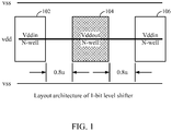
- FIG. 1 shows typical layout (Physical Design) structure of 1-bit (with single input signal) VLS cell which is can be placed next to another cell of input voltage domain (V DD in).
- the FIG. 1 conventional one-bit VLS circuit requires three N-wells, two V DD in N-well 102 and 106 and a V DD out N-well 104 for bit 0. This allows circuits that work at different voltages to properly interface with each other without additional leakage power.
- the adjacent N-wells in the FIG. 1 VLS have alternating different voltages
- design rules require these adjacent N-wells have a minimum spacing for correct functional operation.
- the minimum spacing between the two N-wells 102 and 104 is 0.8 ⁇ m.
- the minimum spacing between the other two N-wells 104 and 106 is also 0.8 ⁇ m.
- FIG. 5 depicts a functional circuit diagram of a conventional 1-bit VLS layout.
- a conventional VLS cell can employ two stage complementary metal-oxide-semiconductor (CMOS) circuits, with a first stage operating at a first voltage 501, as shown by V DD in in FIG. 5 , and a second stage operating at a second voltage 502, as shown by V DD out.
- CMOS complementary metal-oxide-semiconductor
- the conventional VLS may occupy large layout areas because a first N-well for a CMOS transistor in the first stage is coupled to a first voltage, while a second N-well for a CMOS transistor in the second state is coupled to a second voltage, therefore the first and second N-wells have to be separated and have to maintain a certain distance, which is determined by the technology being used.
- FIG. 2 shows a conventional N-well arrangement for a conventional two-bit V DDin (e.g., 0.7 V) to V DDout (e.g., 1.2 V) VLS circuit.
- the FIG. 2 conventional two-bit VLS circuit requires five N-wells, namely one shared V DD in N-well 206, a V DD in N-well 202 and a V DD out N-well 204 for bit 0, and V DD out N-well 208 and V DD in N-well 210 for bit 1. Similar to FIG. 1 , this example illustrates that a minimum spacing between each N-wells 202, 204, 206, 208 and 210 to be at least 0.8 ⁇ m.
- FIG. 2 shows, for example, a minimum spacing of 0.8 ⁇ m.
- this minimum spacing requirement between VLS adjacent N-wells does not fully scale with the feature size. For example, if an IC implemented in 65 nm technology is scaled down to 32 nm (i.e., scaled down by approximately half), the minimum spacing between adjacent N-wells of the IC's VLS circuits does not likewise scale by half.
- level shifter layout design Technology node Cell area (sq. um) Area scaling from previous node 65nm 21.6 NA 45nm 12.3 57% 32nm 7.6 61%
- level shifter circuit incurs significant area overhead compared to regular CMOS logic.
- multiple level shifter instances are placed together they result in multiple N-well voltage islands as shown in FIG. 2 .
- Larger layout footprint increases length of both the internal and external interconnects length increasing dynamic power as well as die area.
- Embodiments of the present invention seek to provide a VLS that operate for different voltage levels and that provides area and power savings for multi-bit implementation of level shifter design.
- Embodiments of the present invention do not rely on particular transistor level circuit implementation of level shifters and may be applied to any possible level shifter circuit styles.
- Embodiments of the present invention are not limited to level shifter circuits, and are applicable to any generic layout design for multi-voltage circuits.
- the present invention can be extended to any circuit requiring two or more different voltage domains and hence multiple N-well islands in the design.
- Embodiments of the present invention relate to a physical design methodology for compact layout of VLS cells in multiple bits.
- the present invention utilizes the presence of separate voltage N-well islands inside a cell.
- Several key physical designs are used to improve design robustness and lower the power dissipation.
- the present invention can allow for a more compact layout of VLS cells in multiple bits.
- the present invention can allow for improved design robustness and low voltage performance, which includes better V DD min.
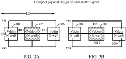
- FIG. 3A and 3B shows two embodiments of the present invention. These embodiments use area efficient physical design for a 2-bit VLS with a pair of input and output signals.
- FIG. 3A and 3B illustrate example of large area saving which is achieved by merging two identical 1-bit level shifter layouts differently than a conventional 1-bit layout, as illustrated in FIG. 1 .
- the 1-bit component layouts are not self-sufficient and cannot be used solely as a compact 1-bit level shifter layout design. Therefore, the embodiments illustrated in FIG. 3A and 3B are examples for a 2-bit VLS, which include two combined component 1-bit level shifter layouts.
- FIG. 3A and 3B shows two embodiments of the present invention. These embodiments use area efficient physical design for a 2-bit VLS with a pair of input and output signals.
- FIG. 3A and 3B illustrate example of large area saving which is achieved by merging two identical 1-bit level shifter layouts differently than a conventional 1-bit layout, as illustrated in FIG. 1 .
- the 1-bit component layouts
- the component 1-bit level shifter layouts is composed of one N-well separation between the N-wells and two standard cell row, which has two Vss and one V DD power rail.
- the component 1-bit level shifter layouts is composed of two N-well separations between the N-wells and one standard cell row, which has one V SS and one V DD power rail.
- table 2 in both embodiments, there can be a forty percent area savings as compared to two separate 1-bit VLS cells as illustrated in FIG. 2 .
- This embodiment forms a two-bit VLS circuit using three (3) N-wells, instead of the five (5) required in the conventional arrangements shown at FIG. 2 .
- the overall width, L2 is approximately half (1 ⁇ 2) of the L1 width of the conventional arrangement shown in FIG. 2 .
- the FIG. 3A embodiment uses a center N-well 302, biased at V DD out, and one N-well biased at V DD in on either side of the center N-well 304, namely N-well 304 at the left and N-well 306 at the right.
- the spacing SP1 between the differently biased N-wells 304 and 302 is the same as between the differently biased N-wells 302 and 306.
- the spacing SP1 may be substantially the same as the spacing between adjacent N-wells in the conventional arrangement of the related art FIG. 2 .
- the FIG. 3A embodiment employs the center N-well 302, biased at V DD out, for the V DD out portion of both the bit 1 and the bit 2 VLS sections of the two-bit VLS circuit.
- the FIG. 3A embodiment employs the left N-well 304 for only the bit 1 VLS section, and the right N-well 306 for only the bit 2 VLS section.
- FIG. 3B shows another embodiment, having the same N-well arrangement as the FIG. 3A embodiment, but employing all three N-wells 302, 304 and 306 for both the bit 1 VLS section and the bit 2 VLS section.
- the 1-bit component layouts are not self-sufficient and cannot be used as compact 1-bit level shifter layout design.
- the component 1-bit level shifter layouts from FIG. 3A comprises of only one N-well separation between them and two standard cell row, which has two V SS and one V DD power rail.
- the component 1-bit level shifter layouts, from FIG. 3B comprises of two N-well separations between them and of only one standard cell row, which has one V SS and one V DD power rail.
- FIG. 4 illustrates a physical design method of a 4-bit VLS.
- table 2 with the FIG. 4 embodiment, there can be a fifty percent area savings as compared to four separate 1-bit VLS cells as illustrated by having two 2-bit VLS, as shown in FIG. 2 , side-by-side.
- the component 1-bit level shifter layouts are composed of only one N-well separation between the N-wells and of only 1 standard cell row, which has one V SS and one V DD power rail per bit.
- Each component 1-bit level shifter is merged both vertically and horizontally together to form a design rule checker clean physical design of a 4-bit VLS.
- the 1-bit component layout is not design rule checker clean and cannot be used as compact 1-bit level shifter layout design by itself.
- Additional advantages of the embodiment depicted in FIG. 4 are that in a multi-bit design, shared clamp or isolation circuitry, if needed can further reduce area and power saving. Also, symmetrical design and placement of critical devices can ensure better design robustness and low voltage performance from device variation (e.g., in a V DD min point of view). Smaller length of interconnects between different bits reduces the capacitive loading and hence the dynamic power dissipation of this embodiment compared to conventional physical design implementation.
- the VLS is essentially a superposed combination of the FIG. 3A and 3B embodiments, achieving a four-bit VLS with the same general arrangement of three N-wells.
- the FIG. 4 embodiment employs the center N-well 402 for all four one-bit sections of the VLS, i.e., for each of the bit 1, bit 2, bit 3 and bit 4 VLS sections.
- the left N-well 404 is employed for both the bit 1 and bit 2 VLS sections, similar to the left N-well 304 of the FIG. 3B embodiment being employed for the bit 1 and bit 2 sections of its two-bit VLS.
- the spacing SP2 between the differently biased N-wells 402 and 404 may be the same as between the differently biased N-wells 404 and 406, and may be substantially the same as SP1 of the FIG. 3A and 3B embodiments.
- the N-wells 402, 404 and 406 may be somewhat larger in area than the N-wells 302, 304 and 306 of the FIG. 3A and 3B embodiments.
- the overall length L3 may be approximately twice L2 of the FIG. 3A and 3B embodiments.
- the FIG. 4 embodiment may be approximately the same area size as the conventional layout shown in FIG. 2 , which is a two-bit VLS comprising of five N-wells. Table 2. Area saving with compact multi-bit level shifter layout methodology in recent semiconductor manufacturing technologies Cell Type 45nm area saving 32nm area saving 2-bit 40% 45 % 4-bit 52% 55%
- the present invention allows for a compact hierarchical physical design methodology to improve multi-rail VLS standard cell design.
- the present invention does not rely on any particular circuit implementation of level shifter and can be applied to all possible level shifter circuit styles.
- the present invention can consist of stitching together to produce an error free design from several symmetrical components in different orientation that are not individually self-sufficient in design.
- the present invention is not limited to voltage level shifter cells, and can be applied to a number of different cell families that involves multiple N-well islands.
- the present invention is not limited to any particular standard cell architecture and can easily be adapted to different cell architecture and style.
- the present invention can be scalable to future process technology nodes with smaller geometries and larger context sensitivity.
- the present invention can be successfully employed in two different standard cell architecture, such as, but not limited to 45nm and 32nm technology nodes.
- the present invention can demonstrate significant area (e.g., over 50%) and power savings for multi-bit implementation of VLS design technologies, including but not limited to 45nm, 32nm and smaller process technologies.
- a software module may reside in RAM memory, flash memory, ROM memory, EPROM memory, EEPROM memory, registers, hard disk, a removable disk, a CD-ROM, or any other form of storage medium known in the art.
- An exemplary storage medium is coupled to the processor such that the processor can read information from, and write information to, the storage medium. In the alternative, the storage medium may be integral to the processor.
- an embodiment of the invention can include a computer readable media embodying a method for compact and robust voltage level shifters design. Accordingly, the invention is not limited to illustrated examples and any means for performing the functionality described herein are included in embodiments of the invention.
Landscapes
- Engineering & Computer Science (AREA)
- Computer Hardware Design (AREA)
- Physics & Mathematics (AREA)
- Computing Systems (AREA)
- General Engineering & Computer Science (AREA)
- Mathematical Physics (AREA)
- Semiconductor Integrated Circuits (AREA)
- Design And Manufacture Of Integrated Circuits (AREA)
- Logic Circuits (AREA)
- Metal-Oxide And Bipolar Metal-Oxide Semiconductor Integrated Circuits (AREA)
Claims (15)
- Eine Multi- bzw. Mehrfachspannungsschaltung zum Verschieben jedes von zwei Bits von einer ersten Spannungspegellogik auf eine zweite Spannungspegellogik, die Folgendes aufweist:eine erste N-Well bzw. n-dotierte Wanne, die in einem Substrat ausgebildet ist;eine zweite n-dotierte Wanne, die in dem Substrat ausgebildet ist, angrenzend an eine Seite der ersten N-dotierten Wanne;eine dritte n-dotierte Wanne, die in dem Substrat ausgebildet ist, angrenzend an eine Seite der ersten n-dotierten Wanne gegenüber der zweiten n-dotierten Wanne;dadurch gekennzeichnet, dass eine erste Ein-Bit-Spannungspegelschieber- bzw. -VLS-Schaltung (VLS = Voltage Level Shifter) einen Teil hat, der auf der ersten n-dotierten Wanne ausgebildet ist und einen Teil, der auf der zweiten n-dotierten Wanne ausgebildet ist; undeine zweite Ein-Bit-VLS-Schaltung mit einem Teil, der auf der ersten n-dotierten Wanne ausgebildet ist und einem Teil, der auf der dritten n-dotierten Wanne ausgebildet ist.
- Mehrfachspannungsschaltung nach Anspruch 1, wobei die Mehrfachspannungsschaltung ein Spannungspegelschieber, eine Isolationszelle, ein Retentions- bzw. Speicherregister oder eine Always-On- bzw. Immer-An-Logikkomponente ist, die in wenigstens einen Halbleiterchip integriert ist.
- Mehrfachspannungsschaltung nach Anspruch 1, wobei die erste, zweite und dritte n-dotierte Wanne in einer Reihe angeordnet sind, wobei die erste n-dotierte Wanne in einer mittleren Position ist.
- Mehrfachspannungsschaltung nach Anspruch 1, wobei die erste n-dotierte Wanne auf den zweiten Spannungspegel vorgespannt ist und wobei die zweite und dritte n-dotierte Wanne auf den ersten Spannungspegel vorgespannt sind.
- Mehrfachspannungsschaltung nach Anspruch 4, wobei die Mehrfachspannungsschaltung eine Separation n-dotierter Wannen zwischen den n-dotierten Wannen hat und aus zwei Standardzellenreihen besteht, die zwei VSS- und eine VDD-Powerrail bzw. -Stromschiene beinhaltet.
- Mehrfachspannungsschaltung nach Anspruch 1, wobei die erste n-dotierte Wanne auf den ersten Spannungspegel vorgespannt ist, und die zweite n-dotierte Wanne und die dritte N-dotierte Wanne auf den zweiten Spannungspegel vorgespannt sind.
- Mehrfachspannungsschaltung nach Anspruch 6, wobei die Mehrfachspannungsschaltung Separationen n-dotierter Wannen zwischen den n-dotierten Wannen hat und eine Standardzellenreihe aufweist, die eine VSS- und eine VDD-Stromschiene beinhaltet.
- Mehrfachspannungsschaltung nach Anspruch 1, wobei die Mehrfachspannungsschaltung eine Vier-Bit-Mehrfachspannungsschaltung zum Verschieben von jedem von vier Bits von einer ersten Spannungspegellogik auf eine zweite Spannungspegellogik ist, die Folgendes aufweist:eine erste N-Well bzw. n-dotierte Wanne, die in einem Substrat ausgebildet ist;eine zweite n-dotierte Wanne, die in dem Substrat ausgebildet ist, angrenzend zu einer Seite der ersten n-dotierten Wanne;eine dritte n-dotierte Wanne, die in dem Substrat ausgebildet ist, angrenzend zu einer Seite der ersten n-dotierten Wanne gegenüber der zweiten n-dotierten Wanne;eine erste Ein-Bit-VLS-Schaltung mit einem Teil, der auf der ersten n-dotierten Wanne ausgebildet ist und einem Teil, der auf der zweiten n-dotierten Wanne ausgebildet ist;eine zweite Ein-Bit-VLS-Schaltung mit einem Teil, der auf der ersten n-dotierten Wanne ausgebildet ist und einem Teil, der auf der zweiten n-dotierten Wanne ausgebildet ist;eine dritte Ein-Bit-VLS-Schaltung mit einem Teil, der auf der ersten n-dotierten Wanne ausgebildet ist und einem Teil, der auf der dritten n-dotierten Wanne ausgebildet ist; undeine vierte Ein-Bit-VLS-Schaltung mit einem Teil, der auf der ersten n-dotierten Wanne ausgebildet ist und einem Teil, der auf der dritten n-dotierten Wanne ausgebildet ist.
- Vier-Bit-Mehrfachspannungsschaltung nach Anspruch 8, wobei die Mehrfachspannungsschaltung ein Spannungspegelschieber, eine Isolationszelle, ein Retentions- bzw. Speicherregister oder eine Always-On- bzw. Immer-An-Logikkomponente ist.
- Vier-Bit-Mehrfachspannungsschaltung nach Anspruch 8, wobei die erste, zweite und dritte n-dotierte Wanne in einer Reihe angeordnet sind, wobei die erste n-dotierte Wanne in einer mittleren Position ist.
- Vier-Bit-Mehrfachspannungsschaltung nach Anspruch 8, wobei die erste n-dotierte Wanne auf den zweiten Spannungspegel vorgespannt ist und die zweiten und dritten n-dotierten Wannen auf den ersten Spannungspegel vorgespannt sind.
- Vier-Bit-Mehrfachspannungsschaltung nach Anspruch 8, wobei die erste n-dotierte Wanne auf den ersten Spannungspegel vorgespannt ist und die zweite und dritte n-dotierte Wanne auf den zweiten Spannungspegel vorgespannt sind.
- Vier-Bit-Mehrfachspannungsschaltung nach Anspruch 8, wobei jedes Ein-Bit-Pegelschieberlayout in der Mehrfachspannungsschaltung aus nur einer Separation n-dotierter Wannen zwischen den n-dotierten Wannen und aus nur einer Standardzellenreihe zusammengesetzt ist, die eine VSS- und eine VDD-Stromschiene pro Bit beinhaltet.
- Ein Verfahren zum Schalten von Leistung in einer Zwei-Bit-Mehrfachspannungsschaltung zum Verschieben jedes von zwei Bits von einer ersten Spannungspegellogik auf eine zweite Spannungspegellogik, wobei eine erste N-Well bzw. n-dotierte Wanne in einem Substrat ausgebildet wird, eine zweite n-dotierte Wanne in dem Substrat ausgebildet wird, angrenzend an eine Seite der ersten n-dotierten Wanne, und eine dritte n-dotierte Wanne in dem Substrat gebildet wird, angrenzend an eine Seite der erste n-dotierten Wanne gegenüber der zweiten n-dotierten Wanne, dadurch gekennzeichnet, dass es Folgendes aufweist:Ausbilden einer ersten Ein-Bit-VLS-Schaltung mit einem Teil auf der ersten n-dotierten Wanne und einem Teil, der auf der zweiten n-dotierten Wanne ausgebildet ist; undAusbilden einer zweiten Ein-Bit-VLS-Schaltung mit einem Teil auf der ersten n-dotierten Wanne und einem Teil, der auf der dritten n-dotierten Wanne ausgebildet ist.
- Ein Verfahren zum Schalten von Leistung in einer Vier-Bit-Mehrfachspannungsschaltung zum Verschieben jedes von vier Bits von einer ersten Spannungspegellogik auf eine zweite Spannungspegellogik, wobei eine erste N-Well bzw. n-dotierte Wanne in einem Substrat ausgebildet ist, eine zweite n-dotierte Wanne in dem Substrat ausgebildet ist, angrenzend an eine Seite der ersten n-dotierten Wanne, eine dritte n-dotierte Wanne in dem Substrat ausgebildet ist, angrenzend an eine Seite der ersten n-dotierten Wanne, dadurch gekennzeichnet, dass es Folgendes aufweist:Ausbilden einer ersten Ein-Bit-VLS-Schaltung mit einem Teil auf der ersten n-dotierten Wanne und einem Teil, der auf der zweiten n-dotierten Wanne ausgebildet ist;Ausbilden einer zweiten Ein-Bit-VLS-Schaltung mit einem Teil auf der ersten n-dotierten Wanne und einem Teil, der auf der zweiten n-dotierten Wanne ausgebildet ist;Ausbilden einer dritten Ein-Bit-VLS-Schaltung mit einem Teil auf der ersten n-dotierten Wanne und einem Teil, der auf der dritten n-dotierten Wanne ausgebildet ist; undAusbilden einer vierten Ein-Bit-VLS-Schaltung mit einem Teil auf der ersten n-dotierten Wanne und einem Teil, der auf der dritten n-dotierten Wanne ausgebildet ist.
Applications Claiming Priority (2)
| Application Number | Priority Date | Filing Date | Title |
|---|---|---|---|
| US13/180,598 US8487658B2 (en) | 2011-07-12 | 2011-07-12 | Compact and robust level shifter layout design |
| PCT/US2012/046562 WO2013010043A1 (en) | 2011-07-12 | 2012-07-12 | Compact and robust level shifter layout design |
Publications (2)
| Publication Number | Publication Date |
|---|---|
| EP2732467A1 EP2732467A1 (de) | 2014-05-21 |
| EP2732467B1 true EP2732467B1 (de) | 2017-02-15 |
Family
ID=46679285
Family Applications (1)
| Application Number | Title | Priority Date | Filing Date |
|---|---|---|---|
| EP12747948.3A Revoked EP2732467B1 (de) | 2011-07-12 | 2012-07-12 | Entwurf für einen kompakten und robusten pegelschieber |
Country Status (6)
| Country | Link |
|---|---|
| US (1) | US8487658B2 (de) |
| EP (1) | EP2732467B1 (de) |
| JP (2) | JP5940660B2 (de) |
| KR (1) | KR101705707B1 (de) |
| CN (1) | CN103765581B (de) |
| WO (1) | WO2013010043A1 (de) |
Families Citing this family (13)
| Publication number | Priority date | Publication date | Assignee | Title |
|---|---|---|---|---|
| US8487658B2 (en) | 2011-07-12 | 2013-07-16 | Qualcomm Incorporated | Compact and robust level shifter layout design |
| US20150109045A1 (en) * | 2013-10-21 | 2015-04-23 | Qualcomm Incorporated | Scalable layout architecture for metal-programmable voltage level shifter cells |
| US9379705B2 (en) * | 2014-02-21 | 2016-06-28 | Samsung Electronics Co., Ltd. | Integrated circuit and semiconductor device including the same |
| KR102147353B1 (ko) * | 2014-02-21 | 2020-08-24 | 삼성전자 주식회사 | 집적 회로 및 이를 포함하는 반도체 장치 |
| US9483600B2 (en) * | 2014-03-14 | 2016-11-01 | Qualcomm Incorporated | Multi supply cell arrays for low power designs |
| KR102368073B1 (ko) | 2015-09-24 | 2022-02-25 | 삼성전자주식회사 | 집적 회로 및 이를 포함하는 반도체 장치 |
| US9958918B2 (en) | 2016-05-23 | 2018-05-01 | Qualcomm Incorporated | Systems and methods to separate power domains in a processing device |
| US10394299B2 (en) | 2016-05-23 | 2019-08-27 | Qualcomm Incorporated | Systems and methods to separate power domains in a processing device |
| US10109619B2 (en) | 2016-06-06 | 2018-10-23 | Qualcomm Incorporated | Methods and apparatus for using split N-well cells in a merged N-well block |
| US12532544B2 (en) * | 2020-10-16 | 2026-01-20 | Synopsys, Inc. | Split N-well cells having a merged N-well design |
| KR20220120047A (ko) * | 2021-02-22 | 2022-08-30 | 삼성전자주식회사 | 전압 레벨 쉬프터 셀 및 이를 포함하는 집적 회로 |
| CN113992201B (zh) * | 2021-10-29 | 2025-07-15 | 海光信息技术股份有限公司 | 一种电平转换电路及其版图结构、标准单元、芯片 |
| US12353261B2 (en) | 2021-11-30 | 2025-07-08 | Qualcomm Incorporated | Neural-network-based power management for neural network loads |
Citations (3)
| Publication number | Priority date | Publication date | Assignee | Title |
|---|---|---|---|---|
| US5780881A (en) | 1995-03-30 | 1998-07-14 | Seiko Epson Corporation | Gate array driven by source voltages and electronic equipment using the same |
| US20090108904A1 (en) * | 2007-10-24 | 2009-04-30 | Shiffer Ii James David | Shifting of a voltage level between different voltage level domains |
| WO2013010043A1 (en) | 2011-07-12 | 2013-01-17 | Qualcomm Incorporated | Compact and robust level shifter layout design |
Family Cites Families (19)
| Publication number | Priority date | Publication date | Assignee | Title |
|---|---|---|---|---|
| US6414518B1 (en) | 1996-05-28 | 2002-07-02 | Altera Corporation | Circuitry for a low internal voltage integrated circuit |
| US6974978B1 (en) * | 1999-03-04 | 2005-12-13 | Intel Corporation | Gate array architecture |
| US6967518B2 (en) | 2002-06-12 | 2005-11-22 | International Rectifier Corporation | High voltage level shifting IC with under-ground voltage swing withstanding capability |
| JP4036688B2 (ja) * | 2002-06-18 | 2008-01-23 | 松下電器産業株式会社 | 自動配置配線用スタンダードセルライブラリ及び半導体集積装置 |
| US7095063B2 (en) | 2003-05-07 | 2006-08-22 | International Business Machines Corporation | Multiple supply gate array backfill structure |
| JP4738719B2 (ja) | 2003-05-09 | 2011-08-03 | ルネサスエレクトロニクス株式会社 | 半導体回路装置の設計方法、設計された半導体回路装置、設計システム、及び記録媒体 |
| US7408269B2 (en) | 2004-06-14 | 2008-08-05 | International Business Machines Corporation | Multi-level power supply system for a complementary metal oxide semiconductor circuit |
| JP2006074631A (ja) * | 2004-09-03 | 2006-03-16 | Koninkl Philips Electronics Nv | レベルシフタ及び電圧変換装置 |
| JP2007173485A (ja) * | 2005-12-21 | 2007-07-05 | Sharp Corp | 半導体集積回路、レベルシフタセル、隙間セルおよび半導体集積回路におけるクロストークノイズを防止する方法。 |
| US8228092B2 (en) * | 2006-09-15 | 2012-07-24 | Texas Instruments Northern Virginia Incorporated | High voltage latching and DC restoration isolation and level shifting method and apparatus |
| US9608604B2 (en) | 2006-12-14 | 2017-03-28 | Taiwan Semiconductor Manufacturing Co., Ltd. | Voltage level shifter with single well voltage |
| US20080265936A1 (en) | 2007-04-27 | 2008-10-30 | Dsm Solutions, Inc. | Integrated circuit switching device, structure and method of manufacture |
| JP4603030B2 (ja) | 2007-11-12 | 2010-12-22 | パナソニック株式会社 | 半導体装置 |
| JP5259246B2 (ja) * | 2008-05-09 | 2013-08-07 | ルネサスエレクトロニクス株式会社 | 半導体装置 |
| JP2010199640A (ja) | 2009-02-20 | 2010-09-09 | Toshiba Corp | 信号レベル変換回路 |
| JP2010218671A (ja) | 2009-03-19 | 2010-09-30 | Renesas Electronics Corp | 半導体記憶装置 |
| US8174288B2 (en) * | 2009-04-13 | 2012-05-08 | International Business Machines Corporation | Voltage conversion and integrated circuits with stacked voltage domains |
| JP2010251445A (ja) * | 2009-04-14 | 2010-11-04 | Hitachi Ltd | 半導体装置およびそれを用いた情報処理装置 |
| GB2471572B (en) | 2009-07-02 | 2015-04-22 | Advanced Risc Mach Ltd | Voltage level shifter |
-
2011
- 2011-07-12 US US13/180,598 patent/US8487658B2/en not_active Expired - Fee Related
-
2012
- 2012-07-12 CN CN201280041547.5A patent/CN103765581B/zh not_active Expired - Fee Related
- 2012-07-12 WO PCT/US2012/046562 patent/WO2013010043A1/en not_active Ceased
- 2012-07-12 KR KR1020147003557A patent/KR101705707B1/ko not_active Expired - Fee Related
- 2012-07-12 JP JP2014520346A patent/JP5940660B2/ja not_active Expired - Fee Related
- 2012-07-12 EP EP12747948.3A patent/EP2732467B1/de not_active Revoked
-
2016
- 2016-05-17 JP JP2016098427A patent/JP2016171335A/ja active Pending
Patent Citations (3)
| Publication number | Priority date | Publication date | Assignee | Title |
|---|---|---|---|---|
| US5780881A (en) | 1995-03-30 | 1998-07-14 | Seiko Epson Corporation | Gate array driven by source voltages and electronic equipment using the same |
| US20090108904A1 (en) * | 2007-10-24 | 2009-04-30 | Shiffer Ii James David | Shifting of a voltage level between different voltage level domains |
| WO2013010043A1 (en) | 2011-07-12 | 2013-01-17 | Qualcomm Incorporated | Compact and robust level shifter layout design |
Non-Patent Citations (1)
| Title |
|---|
| AMIR HASANBEGOVIC ET AL.: "Low- power subthreshold to above thresh- old level shifters in 90 nm and 65 nm process", MICROPROCESSORS AND MI- CROSYSTEMS, vol. 35, 1 February 2011 (2011-02-01), pages 1 - 9, XP055442703 |
Also Published As
| Publication number | Publication date |
|---|---|
| WO2013010043A1 (en) | 2013-01-17 |
| JP2016171335A (ja) | 2016-09-23 |
| JP5940660B2 (ja) | 2016-06-29 |
| CN103765581B (zh) | 2016-11-09 |
| US8487658B2 (en) | 2013-07-16 |
| KR20140046023A (ko) | 2014-04-17 |
| JP2014527287A (ja) | 2014-10-09 |
| EP2732467A1 (de) | 2014-05-21 |
| US20130015882A1 (en) | 2013-01-17 |
| CN103765581A (zh) | 2014-04-30 |
| KR101705707B1 (ko) | 2017-02-10 |
Similar Documents
| Publication | Publication Date | Title |
|---|---|---|
| EP2732467B1 (de) | Entwurf für einen kompakten und robusten pegelschieber | |
| US7310008B1 (en) | Configurable delay chain with stacked inverter delay elements | |
| CN100481451C (zh) | 半导体集成电路装置 | |
| KR101600947B1 (ko) | 전력 도메인들 간의 데이터 트랜스퍼 | |
| US6750555B2 (en) | Semiconductor SRAM having linear diffusion regions | |
| US10552566B2 (en) | Method of designing semiconductor device | |
| JP2010251445A (ja) | 半導体装置およびそれを用いた情報処理装置 | |
| US8488390B2 (en) | Circuits and methods for memory | |
| US8810280B2 (en) | Low leakage spare gates for integrated circuits | |
| US20180367142A1 (en) | Apparatus and methods for leakage current reduction in integrated circuits | |
| US20080043561A1 (en) | Circuit for an sram with reduced power consumption | |
| JP2011054980A (ja) | 半導体集積回路装置 | |
| US7592842B2 (en) | Configurable delay chain with stacked inverter delay elements | |
| US7412679B2 (en) | Semiconductor integrated circuit and semiconductor integrated circuit manufacturing method | |
| US8196073B2 (en) | Structure for reduced area active above-ground and below-supply noise suppression circuits | |
| US7656212B1 (en) | Configurable delay chain with switching control for tail delay elements | |
| US20120124316A1 (en) | Leakage reduction in storage elements via optimized reset states | |
| US7635992B1 (en) | Configurable tapered delay chain with multiple sizes of delay elements | |
| CN105793926B (zh) | 具有双电压非对称存储器单元的芯片及其操作方法和装置 | |
| KR100914553B1 (ko) | 반도체 집적회로 | |
| US9461161B1 (en) | Memory element circuitry with minimum oxide definition width | |
| US20100156462A1 (en) | Programmable logic array and programmable logic array module generator | |
| JUN et al. | CMOS level converter with balanced rise and fall delays | |
| JP2006180327A (ja) | 半導体集積回路 |
Legal Events
| Date | Code | Title | Description |
|---|---|---|---|
| PUAI | Public reference made under article 153(3) epc to a published international application that has entered the european phase |
Free format text: ORIGINAL CODE: 0009012 |
|
| 17P | Request for examination filed |
Effective date: 20140123 |
|
| AK | Designated contracting states |
Kind code of ref document: A1 Designated state(s): AL AT BE BG CH CY CZ DE DK EE ES FI FR GB GR HR HU IE IS IT LI LT LU LV MC MK MT NL NO PL PT RO RS SE SI SK SM TR |
|
| DAX | Request for extension of the european patent (deleted) | ||
| GRAP | Despatch of communication of intention to grant a patent |
Free format text: ORIGINAL CODE: EPIDOSNIGR1 |
|
| INTG | Intention to grant announced |
Effective date: 20160308 |
|
| GRAJ | Information related to disapproval of communication of intention to grant by the applicant or resumption of examination proceedings by the epo deleted |
Free format text: ORIGINAL CODE: EPIDOSDIGR1 |
|
| INTC | Intention to grant announced (deleted) | ||
| GRAS | Grant fee paid |
Free format text: ORIGINAL CODE: EPIDOSNIGR3 |
|
| GRAP | Despatch of communication of intention to grant a patent |
Free format text: ORIGINAL CODE: EPIDOSNIGR1 |
|
| INTG | Intention to grant announced |
Effective date: 20160830 |
|
| STAA | Information on the status of an ep patent application or granted ep patent |
Free format text: STATUS: GRANT OF PATENT IS INTENDED |
|
| GRAA | (expected) grant |
Free format text: ORIGINAL CODE: 0009210 |
|
| STAA | Information on the status of an ep patent application or granted ep patent |
Free format text: STATUS: THE PATENT HAS BEEN GRANTED |
|
| AK | Designated contracting states |
Kind code of ref document: B1 Designated state(s): AL AT BE BG CH CY CZ DE DK EE ES FI FR GB GR HR HU IE IS IT LI LT LU LV MC MK MT NL NO PL PT RO RS SE SI SK SM TR |
|
| REG | Reference to a national code |
Ref country code: CH Ref legal event code: EP Ref country code: GB Ref legal event code: FG4D |
|
| REG | Reference to a national code |
Ref country code: IE Ref legal event code: FG4D |
|
| REG | Reference to a national code |
Ref country code: AT Ref legal event code: REF Ref document number: 868322 Country of ref document: AT Kind code of ref document: T Effective date: 20170315 |
|
| REG | Reference to a national code |
Ref country code: DE Ref legal event code: R096 Ref document number: 602012028709 Country of ref document: DE |
|
| REG | Reference to a national code |
Ref country code: FR Ref legal event code: PLFP Year of fee payment: 6 |
|
| REG | Reference to a national code |
Ref country code: NL Ref legal event code: MP Effective date: 20170215 |
|
| REG | Reference to a national code |
Ref country code: LT Ref legal event code: MG4D |
|
| REG | Reference to a national code |
Ref country code: AT Ref legal event code: MK05 Ref document number: 868322 Country of ref document: AT Kind code of ref document: T Effective date: 20170215 |
|
| PG25 | Lapsed in a contracting state [announced via postgrant information from national office to epo] |
Ref country code: FI Free format text: LAPSE BECAUSE OF FAILURE TO SUBMIT A TRANSLATION OF THE DESCRIPTION OR TO PAY THE FEE WITHIN THE PRESCRIBED TIME-LIMIT Effective date: 20170215 Ref country code: HR Free format text: LAPSE BECAUSE OF FAILURE TO SUBMIT A TRANSLATION OF THE DESCRIPTION OR TO PAY THE FEE WITHIN THE PRESCRIBED TIME-LIMIT Effective date: 20170215 Ref country code: NO Free format text: LAPSE BECAUSE OF FAILURE TO SUBMIT A TRANSLATION OF THE DESCRIPTION OR TO PAY THE FEE WITHIN THE PRESCRIBED TIME-LIMIT Effective date: 20170515 Ref country code: LT Free format text: LAPSE BECAUSE OF FAILURE TO SUBMIT A TRANSLATION OF THE DESCRIPTION OR TO PAY THE FEE WITHIN THE PRESCRIBED TIME-LIMIT Effective date: 20170215 Ref country code: GR Free format text: LAPSE BECAUSE OF FAILURE TO SUBMIT A TRANSLATION OF THE DESCRIPTION OR TO PAY THE FEE WITHIN THE PRESCRIBED TIME-LIMIT Effective date: 20170516 |
|
| PG25 | Lapsed in a contracting state [announced via postgrant information from national office to epo] |
Ref country code: AT Free format text: LAPSE BECAUSE OF FAILURE TO SUBMIT A TRANSLATION OF THE DESCRIPTION OR TO PAY THE FEE WITHIN THE PRESCRIBED TIME-LIMIT Effective date: 20170215 Ref country code: ES Free format text: LAPSE BECAUSE OF FAILURE TO SUBMIT A TRANSLATION OF THE DESCRIPTION OR TO PAY THE FEE WITHIN THE PRESCRIBED TIME-LIMIT Effective date: 20170215 Ref country code: LV Free format text: LAPSE BECAUSE OF FAILURE TO SUBMIT A TRANSLATION OF THE DESCRIPTION OR TO PAY THE FEE WITHIN THE PRESCRIBED TIME-LIMIT Effective date: 20170215 Ref country code: RS Free format text: LAPSE BECAUSE OF FAILURE TO SUBMIT A TRANSLATION OF THE DESCRIPTION OR TO PAY THE FEE WITHIN THE PRESCRIBED TIME-LIMIT Effective date: 20170215 Ref country code: PT Free format text: LAPSE BECAUSE OF FAILURE TO SUBMIT A TRANSLATION OF THE DESCRIPTION OR TO PAY THE FEE WITHIN THE PRESCRIBED TIME-LIMIT Effective date: 20170615 Ref country code: NL Free format text: LAPSE BECAUSE OF FAILURE TO SUBMIT A TRANSLATION OF THE DESCRIPTION OR TO PAY THE FEE WITHIN THE PRESCRIBED TIME-LIMIT Effective date: 20170215 Ref country code: BG Free format text: LAPSE BECAUSE OF FAILURE TO SUBMIT A TRANSLATION OF THE DESCRIPTION OR TO PAY THE FEE WITHIN THE PRESCRIBED TIME-LIMIT Effective date: 20170515 Ref country code: SE Free format text: LAPSE BECAUSE OF FAILURE TO SUBMIT A TRANSLATION OF THE DESCRIPTION OR TO PAY THE FEE WITHIN THE PRESCRIBED TIME-LIMIT Effective date: 20170215 |
|
| PG25 | Lapsed in a contracting state [announced via postgrant information from national office to epo] |
Ref country code: SK Free format text: LAPSE BECAUSE OF FAILURE TO SUBMIT A TRANSLATION OF THE DESCRIPTION OR TO PAY THE FEE WITHIN THE PRESCRIBED TIME-LIMIT Effective date: 20170215 Ref country code: CZ Free format text: LAPSE BECAUSE OF FAILURE TO SUBMIT A TRANSLATION OF THE DESCRIPTION OR TO PAY THE FEE WITHIN THE PRESCRIBED TIME-LIMIT Effective date: 20170215 Ref country code: EE Free format text: LAPSE BECAUSE OF FAILURE TO SUBMIT A TRANSLATION OF THE DESCRIPTION OR TO PAY THE FEE WITHIN THE PRESCRIBED TIME-LIMIT Effective date: 20170215 Ref country code: IT Free format text: LAPSE BECAUSE OF FAILURE TO SUBMIT A TRANSLATION OF THE DESCRIPTION OR TO PAY THE FEE WITHIN THE PRESCRIBED TIME-LIMIT Effective date: 20170215 Ref country code: RO Free format text: LAPSE BECAUSE OF FAILURE TO SUBMIT A TRANSLATION OF THE DESCRIPTION OR TO PAY THE FEE WITHIN THE PRESCRIBED TIME-LIMIT Effective date: 20170215 |
|
| REG | Reference to a national code |
Ref country code: DE Ref legal event code: R026 Ref document number: 602012028709 Country of ref document: DE |
|
| PLBI | Opposition filed |
Free format text: ORIGINAL CODE: 0009260 |
|
| PG25 | Lapsed in a contracting state [announced via postgrant information from national office to epo] |
Ref country code: PL Free format text: LAPSE BECAUSE OF FAILURE TO SUBMIT A TRANSLATION OF THE DESCRIPTION OR TO PAY THE FEE WITHIN THE PRESCRIBED TIME-LIMIT Effective date: 20170215 Ref country code: SM Free format text: LAPSE BECAUSE OF FAILURE TO SUBMIT A TRANSLATION OF THE DESCRIPTION OR TO PAY THE FEE WITHIN THE PRESCRIBED TIME-LIMIT Effective date: 20170215 Ref country code: DK Free format text: LAPSE BECAUSE OF FAILURE TO SUBMIT A TRANSLATION OF THE DESCRIPTION OR TO PAY THE FEE WITHIN THE PRESCRIBED TIME-LIMIT Effective date: 20170215 |
|
| REG | Reference to a national code |
Ref country code: CH Ref legal event code: NV Representative=s name: KASCHE AND PARTNER AG, CH Ref country code: CH Ref legal event code: PUE Owner name: SCIVIS WISSENSCHAFTLICHE BILDVERARBEITUNG GMBH, DE Free format text: FORMER OWNER: QUALCOMM INCORPORATED, US |
|
| PLAX | Notice of opposition and request to file observation + time limit sent |
Free format text: ORIGINAL CODE: EPIDOSNOBS2 |
|
| 26 | Opposition filed |
Opponent name: APPLE INC. Effective date: 20171115 |
|
| PG25 | Lapsed in a contracting state [announced via postgrant information from national office to epo] |
Ref country code: SI Free format text: LAPSE BECAUSE OF FAILURE TO SUBMIT A TRANSLATION OF THE DESCRIPTION OR TO PAY THE FEE WITHIN THE PRESCRIBED TIME-LIMIT Effective date: 20170215 |
|
| REG | Reference to a national code |
Ref country code: CH Ref legal event code: PL |
|
| REG | Reference to a national code |
Ref country code: CH Ref legal event code: PK Free format text: BERICHTIGUNG INHABER |
|
| REG | Reference to a national code |
Ref country code: IE Ref legal event code: MM4A |
|
| PG25 | Lapsed in a contracting state [announced via postgrant information from national office to epo] |
Ref country code: IE Free format text: LAPSE BECAUSE OF NON-PAYMENT OF DUE FEES Effective date: 20170712 Ref country code: CH Free format text: LAPSE BECAUSE OF NON-PAYMENT OF DUE FEES Effective date: 20170731 Ref country code: LI Free format text: LAPSE BECAUSE OF NON-PAYMENT OF DUE FEES Effective date: 20170731 |
|
| PLBB | Reply of patent proprietor to notice(s) of opposition received |
Free format text: ORIGINAL CODE: EPIDOSNOBS3 |
|
| REG | Reference to a national code |
Ref country code: BE Ref legal event code: MM Effective date: 20170731 |
|
| REG | Reference to a national code |
Ref country code: FR Ref legal event code: PLFP Year of fee payment: 7 |
|
| PG25 | Lapsed in a contracting state [announced via postgrant information from national office to epo] |
Ref country code: LU Free format text: LAPSE BECAUSE OF NON-PAYMENT OF DUE FEES Effective date: 20170712 |
|
| PLAB | Opposition data, opponent's data or that of the opponent's representative modified |
Free format text: ORIGINAL CODE: 0009299OPPO |
|
| R26 | Opposition filed (corrected) |
Opponent name: APPLE INC. Effective date: 20171115 |
|
| PG25 | Lapsed in a contracting state [announced via postgrant information from national office to epo] |
Ref country code: BE Free format text: LAPSE BECAUSE OF NON-PAYMENT OF DUE FEES Effective date: 20170731 |
|
| PGFP | Annual fee paid to national office [announced via postgrant information from national office to epo] |
Ref country code: FR Payment date: 20180620 Year of fee payment: 7 |
|
| REG | Reference to a national code |
Ref country code: DE Ref legal event code: R064 Ref document number: 602012028709 Country of ref document: DE Ref country code: DE Ref legal event code: R103 Ref document number: 602012028709 Country of ref document: DE |
|
| PG25 | Lapsed in a contracting state [announced via postgrant information from national office to epo] |
Ref country code: MT Free format text: LAPSE BECAUSE OF NON-PAYMENT OF DUE FEES Effective date: 20170712 |
|
| RDAE | Information deleted related to despatch of communication that patent is revoked |
Free format text: ORIGINAL CODE: EPIDOSDREV1 |
|
| RDAF | Communication despatched that patent is revoked |
Free format text: ORIGINAL CODE: EPIDOSNREV1 |
|
| PGFP | Annual fee paid to national office [announced via postgrant information from national office to epo] |
Ref country code: GB Payment date: 20180625 Year of fee payment: 7 Ref country code: DE Payment date: 20180618 Year of fee payment: 7 |
|
| RDAG | Patent revoked |
Free format text: ORIGINAL CODE: 0009271 |
|
| STAA | Information on the status of an ep patent application or granted ep patent |
Free format text: STATUS: PATENT REVOKED |
|
| 27W | Patent revoked |
Effective date: 20180920 |
|
| GBPR | Gb: patent revoked under art. 102 of the ep convention designating the uk as contracting state |
Effective date: 20180920 |
|
| PG25 | Lapsed in a contracting state [announced via postgrant information from national office to epo] |
Ref country code: MC Free format text: LAPSE BECAUSE OF FAILURE TO SUBMIT A TRANSLATION OF THE DESCRIPTION OR TO PAY THE FEE WITHIN THE PRESCRIBED TIME-LIMIT Effective date: 20170215 |
|
| PG25 | Lapsed in a contracting state [announced via postgrant information from national office to epo] |
Ref country code: MK Free format text: LAPSE BECAUSE OF FAILURE TO SUBMIT A TRANSLATION OF THE DESCRIPTION OR TO PAY THE FEE WITHIN THE PRESCRIBED TIME-LIMIT Effective date: 20170215 |
|
| PG25 | Lapsed in a contracting state [announced via postgrant information from national office to epo] |
Ref country code: CY Free format text: LAPSE BECAUSE OF FAILURE TO SUBMIT A TRANSLATION OF THE DESCRIPTION OR TO PAY THE FEE WITHIN THE PRESCRIBED TIME-LIMIT Effective date: 20170215 |
|
| PG25 | Lapsed in a contracting state [announced via postgrant information from national office to epo] |
Ref country code: AL Free format text: LAPSE BECAUSE OF FAILURE TO SUBMIT A TRANSLATION OF THE DESCRIPTION OR TO PAY THE FEE WITHIN THE PRESCRIBED TIME-LIMIT Effective date: 20170215 Ref country code: IS Free format text: LAPSE BECAUSE OF FAILURE TO SUBMIT A TRANSLATION OF THE DESCRIPTION OR TO PAY THE FEE WITHIN THE PRESCRIBED TIME-LIMIT Effective date: 20170615 |
|
| PG25 | Lapsed in a contracting state [announced via postgrant information from national office to epo] |
Ref country code: TR Free format text: LAPSE BECAUSE OF FAILURE TO SUBMIT A TRANSLATION OF THE DESCRIPTION OR TO PAY THE FEE WITHIN THE PRESCRIBED TIME-LIMIT Effective date: 20170215 |