EP2724371B1 - Integrated circuit design using through silicon vias - Google Patents
Integrated circuit design using through silicon vias Download PDFInfo
- Publication number
- EP2724371B1 EP2724371B1 EP12704155.6A EP12704155A EP2724371B1 EP 2724371 B1 EP2724371 B1 EP 2724371B1 EP 12704155 A EP12704155 A EP 12704155A EP 2724371 B1 EP2724371 B1 EP 2724371B1
- Authority
- EP
- European Patent Office
- Prior art keywords
- tsvs
- tsv
- stress
- interposer
- active circuit
- Prior art date
- Legal status (The legal status is an assumption and is not a legal conclusion. Google has not performed a legal analysis and makes no representation as to the accuracy of the status listed.)
- Active
Links
Images

Classifications
-
- H—ELECTRICITY
- H10—SEMICONDUCTOR DEVICES; ELECTRIC SOLID-STATE DEVICES NOT OTHERWISE PROVIDED FOR
- H10W—GENERIC PACKAGES, INTERCONNECTIONS, CONNECTORS OR OTHER CONSTRUCTIONAL DETAILS OF DEVICES COVERED BY CLASS H10
- H10W72/00—Interconnections or connectors in packages
-
- H—ELECTRICITY
- H10—SEMICONDUCTOR DEVICES; ELECTRIC SOLID-STATE DEVICES NOT OTHERWISE PROVIDED FOR
- H10W—GENERIC PACKAGES, INTERCONNECTIONS, CONNECTORS OR OTHER CONSTRUCTIONAL DETAILS OF DEVICES COVERED BY CLASS H10
- H10W20/00—Interconnections in chips, wafers or substrates
- H10W20/20—Interconnections within wafers or substrates, e.g. through-silicon vias [TSV]
- H10W20/211—Through-semiconductor vias, e.g. TSVs
- H10W20/212—Top-view shapes or dispositions, e.g. top-view layouts of the vias
-
- H—ELECTRICITY
- H10—SEMICONDUCTOR DEVICES; ELECTRIC SOLID-STATE DEVICES NOT OTHERWISE PROVIDED FOR
- H10W—GENERIC PACKAGES, INTERCONNECTIONS, CONNECTORS OR OTHER CONSTRUCTIONAL DETAILS OF DEVICES COVERED BY CLASS H10
- H10W20/00—Interconnections in chips, wafers or substrates
- H10W20/40—Interconnections external to wafers or substrates, e.g. back-end-of-line [BEOL] metallisations or vias connecting to gate electrodes
-
- H—ELECTRICITY
- H10—SEMICONDUCTOR DEVICES; ELECTRIC SOLID-STATE DEVICES NOT OTHERWISE PROVIDED FOR
- H10W—GENERIC PACKAGES, INTERCONNECTIONS, CONNECTORS OR OTHER CONSTRUCTIONAL DETAILS OF DEVICES COVERED BY CLASS H10
- H10W70/00—Package substrates; Interposers; Redistribution layers [RDL]
- H10W70/60—Insulating or insulated package substrates; Interposers; Redistribution layers
- H10W70/611—Insulating or insulated package substrates; Interposers; Redistribution layers for connecting multiple chips together
-
- H—ELECTRICITY
- H10—SEMICONDUCTOR DEVICES; ELECTRIC SOLID-STATE DEVICES NOT OTHERWISE PROVIDED FOR
- H10W—GENERIC PACKAGES, INTERCONNECTIONS, CONNECTORS OR OTHER CONSTRUCTIONAL DETAILS OF DEVICES COVERED BY CLASS H10
- H10W70/00—Package substrates; Interposers; Redistribution layers [RDL]
- H10W70/60—Insulating or insulated package substrates; Interposers; Redistribution layers
- H10W70/62—Insulating or insulated package substrates; Interposers; Redistribution layers characterised by their interconnections
- H10W70/63—Vias, e.g. via plugs
- H10W70/635—Through-vias
-
- H—ELECTRICITY
- H10—SEMICONDUCTOR DEVICES; ELECTRIC SOLID-STATE DEVICES NOT OTHERWISE PROVIDED FOR
- H10W—GENERIC PACKAGES, INTERCONNECTIONS, CONNECTORS OR OTHER CONSTRUCTIONAL DETAILS OF DEVICES COVERED BY CLASS H10
- H10W70/00—Package substrates; Interposers; Redistribution layers [RDL]
- H10W70/60—Insulating or insulated package substrates; Interposers; Redistribution layers
- H10W70/67—Insulating or insulated package substrates; Interposers; Redistribution layers characterised by their insulating layers or insulating parts
- H10W70/69—Insulating materials thereof
- H10W70/698—Semiconductor materials that are electrically insulating, e.g. undoped silicon
-
- H—ELECTRICITY
- H10—SEMICONDUCTOR DEVICES; ELECTRIC SOLID-STATE DEVICES NOT OTHERWISE PROVIDED FOR
- H10W—GENERIC PACKAGES, INTERCONNECTIONS, CONNECTORS OR OTHER CONSTRUCTIONAL DETAILS OF DEVICES COVERED BY CLASS H10
- H10W90/00—Package configurations
-
- H—ELECTRICITY
- H10—SEMICONDUCTOR DEVICES; ELECTRIC SOLID-STATE DEVICES NOT OTHERWISE PROVIDED FOR
- H10W—GENERIC PACKAGES, INTERCONNECTIONS, CONNECTORS OR OTHER CONSTRUCTIONAL DETAILS OF DEVICES COVERED BY CLASS H10
- H10W70/00—Package substrates; Interposers; Redistribution layers [RDL]
- H10W70/60—Insulating or insulated package substrates; Interposers; Redistribution layers
- H10W70/62—Insulating or insulated package substrates; Interposers; Redistribution layers characterised by their interconnections
- H10W70/63—Vias, e.g. via plugs
-
- H—ELECTRICITY
- H10—SEMICONDUCTOR DEVICES; ELECTRIC SOLID-STATE DEVICES NOT OTHERWISE PROVIDED FOR
- H10W—GENERIC PACKAGES, INTERCONNECTIONS, CONNECTORS OR OTHER CONSTRUCTIONAL DETAILS OF DEVICES COVERED BY CLASS H10
- H10W72/00—Interconnections or connectors in packages
- H10W72/071—Connecting or disconnecting
- H10W72/072—Connecting or disconnecting of bump connectors
- H10W72/07251—Connecting or disconnecting of bump connectors characterised by changes in properties of the bump connectors during connecting
- H10W72/07252—Connecting or disconnecting of bump connectors characterised by changes in properties of the bump connectors during connecting changes in structures or sizes
-
- H—ELECTRICITY
- H10—SEMICONDUCTOR DEVICES; ELECTRIC SOLID-STATE DEVICES NOT OTHERWISE PROVIDED FOR
- H10W—GENERIC PACKAGES, INTERCONNECTIONS, CONNECTORS OR OTHER CONSTRUCTIONAL DETAILS OF DEVICES COVERED BY CLASS H10
- H10W72/00—Interconnections or connectors in packages
- H10W72/071—Connecting or disconnecting
- H10W72/072—Connecting or disconnecting of bump connectors
- H10W72/07251—Connecting or disconnecting of bump connectors characterised by changes in properties of the bump connectors during connecting
- H10W72/07254—Connecting or disconnecting of bump connectors characterised by changes in properties of the bump connectors during connecting changes in dispositions
-
- H—ELECTRICITY
- H10—SEMICONDUCTOR DEVICES; ELECTRIC SOLID-STATE DEVICES NOT OTHERWISE PROVIDED FOR
- H10W—GENERIC PACKAGES, INTERCONNECTIONS, CONNECTORS OR OTHER CONSTRUCTIONAL DETAILS OF DEVICES COVERED BY CLASS H10
- H10W72/00—Interconnections or connectors in packages
- H10W72/20—Bump connectors, e.g. solder bumps or copper pillars; Dummy bumps; Thermal bumps
- H10W72/221—Structures or relative sizes
- H10W72/227—Multiple bumps having different sizes
-
- H—ELECTRICITY
- H10—SEMICONDUCTOR DEVICES; ELECTRIC SOLID-STATE DEVICES NOT OTHERWISE PROVIDED FOR
- H10W—GENERIC PACKAGES, INTERCONNECTIONS, CONNECTORS OR OTHER CONSTRUCTIONAL DETAILS OF DEVICES COVERED BY CLASS H10
- H10W72/00—Interconnections or connectors in packages
- H10W72/20—Bump connectors, e.g. solder bumps or copper pillars; Dummy bumps; Thermal bumps
- H10W72/241—Dispositions, e.g. layouts
- H10W72/244—Dispositions, e.g. layouts relative to underlying supporting features, e.g. bond pads, RDLs or vias
-
- H—ELECTRICITY
- H10—SEMICONDUCTOR DEVICES; ELECTRIC SOLID-STATE DEVICES NOT OTHERWISE PROVIDED FOR
- H10W—GENERIC PACKAGES, INTERCONNECTIONS, CONNECTORS OR OTHER CONSTRUCTIONAL DETAILS OF DEVICES COVERED BY CLASS H10
- H10W72/00—Interconnections or connectors in packages
- H10W72/20—Bump connectors, e.g. solder bumps or copper pillars; Dummy bumps; Thermal bumps
- H10W72/241—Dispositions, e.g. layouts
- H10W72/247—Dispositions of multiple bumps
-
- H—ELECTRICITY
- H10—SEMICONDUCTOR DEVICES; ELECTRIC SOLID-STATE DEVICES NOT OTHERWISE PROVIDED FOR
- H10W—GENERIC PACKAGES, INTERCONNECTIONS, CONNECTORS OR OTHER CONSTRUCTIONAL DETAILS OF DEVICES COVERED BY CLASS H10
- H10W90/00—Package configurations
- H10W90/20—Configurations of stacked chips
- H10W90/22—Configurations of stacked chips the stacked chips being on both top and bottom sides of a package substrate, interposer or RDL
-
- H—ELECTRICITY
- H10—SEMICONDUCTOR DEVICES; ELECTRIC SOLID-STATE DEVICES NOT OTHERWISE PROVIDED FOR
- H10W—GENERIC PACKAGES, INTERCONNECTIONS, CONNECTORS OR OTHER CONSTRUCTIONAL DETAILS OF DEVICES COVERED BY CLASS H10
- H10W90/00—Package configurations
- H10W90/20—Configurations of stacked chips
- H10W90/297—Configurations of stacked chips characterised by the through-semiconductor vias [TSVs] in the stacked chips
-
- H—ELECTRICITY
- H10—SEMICONDUCTOR DEVICES; ELECTRIC SOLID-STATE DEVICES NOT OTHERWISE PROVIDED FOR
- H10W—GENERIC PACKAGES, INTERCONNECTIONS, CONNECTORS OR OTHER CONSTRUCTIONAL DETAILS OF DEVICES COVERED BY CLASS H10
- H10W90/00—Package configurations
- H10W90/701—Package configurations characterised by the relative positions of pads or connectors relative to package parts
- H10W90/721—Package configurations characterised by the relative positions of pads or connectors relative to package parts of bump connectors
- H10W90/722—Package configurations characterised by the relative positions of pads or connectors relative to package parts of bump connectors between stacked chips
-
- H—ELECTRICITY
- H10—SEMICONDUCTOR DEVICES; ELECTRIC SOLID-STATE DEVICES NOT OTHERWISE PROVIDED FOR
- H10W—GENERIC PACKAGES, INTERCONNECTIONS, CONNECTORS OR OTHER CONSTRUCTIONAL DETAILS OF DEVICES COVERED BY CLASS H10
- H10W90/00—Package configurations
- H10W90/701—Package configurations characterised by the relative positions of pads or connectors relative to package parts
- H10W90/721—Package configurations characterised by the relative positions of pads or connectors relative to package parts of bump connectors
- H10W90/724—Package configurations characterised by the relative positions of pads or connectors relative to package parts of bump connectors between a chip and a stacked insulating package substrate, interposer or RDL
-
- H—ELECTRICITY
- H10—SEMICONDUCTOR DEVICES; ELECTRIC SOLID-STATE DEVICES NOT OTHERWISE PROVIDED FOR
- H10W—GENERIC PACKAGES, INTERCONNECTIONS, CONNECTORS OR OTHER CONSTRUCTIONAL DETAILS OF DEVICES COVERED BY CLASS H10
- H10W90/00—Package configurations
- H10W90/701—Package configurations characterised by the relative positions of pads or connectors relative to package parts
- H10W90/751—Package configurations characterised by the relative positions of pads or connectors relative to package parts of bond wires
- H10W90/752—Package configurations characterised by the relative positions of pads or connectors relative to package parts of bond wires between stacked chips
-
- H—ELECTRICITY
- H10—SEMICONDUCTOR DEVICES; ELECTRIC SOLID-STATE DEVICES NOT OTHERWISE PROVIDED FOR
- H10W—GENERIC PACKAGES, INTERCONNECTIONS, CONNECTORS OR OTHER CONSTRUCTIONAL DETAILS OF DEVICES COVERED BY CLASS H10
- H10W90/00—Package configurations
- H10W90/701—Package configurations characterised by the relative positions of pads or connectors relative to package parts
- H10W90/751—Package configurations characterised by the relative positions of pads or connectors relative to package parts of bond wires
- H10W90/754—Package configurations characterised by the relative positions of pads or connectors relative to package parts of bond wires between a chip and a stacked insulating package substrate, interposer or RDL
Definitions
- TSV through silicon via
- Each TSV can be characterized as a vertical conductive path that extends through a die of the multi-die IC structure.
- Each TSV can be used to electrically couple a node on a top surface of the die through which the TSV extends with a different node on a bottom surface of the same die.
- a TSV can be used to couple a node of a first die located above a second die including the TSV with a node of a third die located below the second die or a node of the IC package located below the second die.
- JP 2004-342724A deals with homogenization of stress added to a MISFET structure.
- the method can include determining, using a processor, that a stress field to which a first active circuit element of a circuit block is exposed and a stress field to which a second active circuit element of the circuit block is exposed are mismatched.
- the method can include reducing mismatch between the stress field of the first active circuit element and the stress field of the second active circuit element by modifying a layout of the die for a TSV.
- Reducing mismatch can include adjusting a location of the TSV, wherein the TSV contributes to the stress field of either the first active circuit element or the second active circuit element.
- adjusting a location of the TSV can include adjusting a location of the TSV creating a symmetric TSV and circuit block configuration.
- Determining that the stress field to which the first active circuit element is exposed and the stress field to which the second active circuit element is exposed are mismatched can include determining mismatch according to symmetry of the circuit block with respect to the TSV. Additionally or alternatively, determining that the stress field to which the first active circuit element is exposed and the stress field to which the second active circuit element is exposed are mismatched can include determining mismatch according to distance of the TSV to the first active circuit element and the second active circuit element.
- Reducing mismatch can include adjusting a location of the TSV, wherein the TSV contributes to the stress field of either the first active circuit element or the second active circuit element.
- adjusting a location of a TSV can include adjusting a location of the TSV creating a symmetric TSV and circuit block configuration.
- TSVs through silicon vias
- the use or inclusion of TSVs within an IC can have an effect upon the performance of the circuitry implemented therein.
- the inclusion of a TSV for example, can induce or generate a stress field within the particular die within which the TSV is implemented.
- the stress field induced by the TSV can influence the performance of an active circuit element and, thus, by extension, more complex circuits or circuit blocks built using active circuit elements such as transistors.
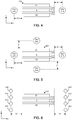
- FIG. 1 is a first block diagram illustrating a topographic view of a multi-die IC structure (IC structure) 100.
- IC structure 100 illustrates a packing approach to stacking multiple dies of an IC within a single package.
- IC structure 100 can include a silicon interposer (interposer) 105, a die 110, and a die 115.
- interposer silicon interposer
- Interposer 105 can be manufactured using one or more additional process steps that allow the deposition of one or more dielectric or insulating layer(s) such as, for example, silicon dioxide.
- interposer 105 can be manufactured using one or more additional process steps that allow the creation of active circuit elements such as, for example, transistor devices and/or diode devices.
- interposer 105 is, in general, a die and is characterized by the presence of one or more TSVs as will be described in greater detail within this specification.
- Solder bumps 220 can be used to electrically couple interposer 105 to a surface 235.
- Surface 235 can represent, for example, a multi-die IC package in which IC structure 100 is implemented. Solder bumps 220 further can couple IC structure 100 directly to a node external to the multi-die IC package.
- solder bumps 220 can be used to physically attach interposer 105 to surface 235.
- TSVs 225 represent vias that, when filled with conductive material, form an electrical connection that vertically transverses, e.g., extends through a substantial portion, if not the entirety of, interposer 105.
- TSVs 225 can be implemented by drilling or etching an opening into interposer 105 that extends from a first planar surface, i.e., the surface to which solder bumps 205 are coupled, through to a second planar surface, i.e., the surface to which solder bumps 220 are coupled. Conductive material then can be deposited within TSVs 225. Examples of conductive material that can be used to fill TSVs 225 can include, but are not limited to, copper, aluminum, gold, copper, nickel, various silicides, and/or the like. In another example, TSVs 225 can traverse substantially through interposer 105 to couple solder bumps 220 with one or more metal layers as are used to form interconnect 215. Interconnect 215 and one or more conventional vias then can couple TSVs 225 to solder bumps 205.
- a uni-axial force is applied to interposer 105 along edges 315 and 320.
- the application of force to interposer 105 generates tensile stress within the material used to implement interposer 105.
- the force applied to an area of an edge of interposer 105 is illustrated by each of arrows 305.
- Tensile stress (stress) present within interposer 105 is illustrated by each of arrows 310.
- the orientation and length of each of arrows 305 demonstrate the direction and magnitude, respectively, of the force applied to edges 315 and 320 of interposer 105.
- the orientation and length of each of arrows 310 demonstrate the direction and magnitude, respectively, of the stress generated within various areas of interposer 105.
Landscapes
- Semiconductor Integrated Circuits (AREA)
- Design And Manufacture Of Integrated Circuits (AREA)
- Internal Circuitry In Semiconductor Integrated Circuit Devices (AREA)
Applications Claiming Priority (2)
| Application Number | Priority Date | Filing Date | Title |
|---|---|---|---|
| US13/170,020 US8560982B2 (en) | 2011-06-27 | 2011-06-27 | Integrated circuit design using through silicon vias |
| PCT/US2012/021416 WO2013002844A1 (en) | 2011-06-27 | 2012-01-16 | Integrated circuit design using through silicon vias |
Publications (2)
| Publication Number | Publication Date |
|---|---|
| EP2724371A1 EP2724371A1 (en) | 2014-04-30 |
| EP2724371B1 true EP2724371B1 (en) | 2017-08-30 |
Family
ID=45607357
Family Applications (1)
| Application Number | Title | Priority Date | Filing Date |
|---|---|---|---|
| EP12704155.6A Active EP2724371B1 (en) | 2011-06-27 | 2012-01-16 | Integrated circuit design using through silicon vias |
Country Status (6)
| Country | Link |
|---|---|
| US (1) | US8560982B2 (enExample) |
| EP (1) | EP2724371B1 (enExample) |
| JP (1) | JP6009556B2 (enExample) |
| KR (1) | KR101770877B1 (enExample) |
| CN (1) | CN103688355B (enExample) |
| WO (1) | WO2013002844A1 (enExample) |
Families Citing this family (21)
| Publication number | Priority date | Publication date | Assignee | Title |
|---|---|---|---|---|
| US8264065B2 (en) * | 2009-10-23 | 2012-09-11 | Synopsys, Inc. | ESD/antenna diodes for through-silicon vias |
| US8766459B2 (en) * | 2010-05-03 | 2014-07-01 | Georgia Tech Research Corporation | CMUT devices and fabrication methods |
| US8604619B2 (en) * | 2011-08-31 | 2013-12-10 | Taiwan Semiconductor Manufacturing Company, Ltd. | Through silicon via keep out zone formation along different crystal orientations |
| US20130132023A1 (en) * | 2011-11-17 | 2013-05-23 | Advanced Micro Devices, Inc. | Structure for characterizing through-silicon vias and methods thereof |
| US8664768B2 (en) * | 2012-05-03 | 2014-03-04 | Taiwan Semiconductor Manufacturing Company, Ltd. | Interposer having a defined through via pattern |
| US9026872B2 (en) * | 2012-08-16 | 2015-05-05 | Xilinx, Inc. | Flexible sized die for use in multi-die integrated circuit |
| US9997443B2 (en) | 2013-02-25 | 2018-06-12 | Infineon Technologies Ag | Through vias and methods of formation thereof |
| US9030025B2 (en) | 2013-03-15 | 2015-05-12 | IPEnval Consultant Inc. | Integrated circuit layout |
| US8952500B2 (en) | 2013-03-15 | 2015-02-10 | IPEnval Consultant Inc. | Semiconductor device |
| US8957504B2 (en) | 2013-03-15 | 2015-02-17 | IP Enval Consultant Inc. | Integrated structure with a silicon-through via |
| US9547034B2 (en) | 2013-07-03 | 2017-01-17 | Xilinx, Inc. | Monolithic integrated circuit die having modular die regions stitched together |
| EP3160445B1 (en) | 2014-06-26 | 2021-10-20 | Island Breeze Systems Ca, LLC | Mdi related products and methods of use |
| US10713406B2 (en) * | 2015-11-30 | 2020-07-14 | The Regents Of The University Of California | Multi-die IC layout methods with awareness of mix and match die integration |
| CN105866665B (zh) * | 2016-03-31 | 2019-04-05 | 复旦大学 | 面向高性能SoC FPGA的功能遍历测试方法 |
| US10497677B1 (en) | 2017-02-09 | 2019-12-03 | Xilinx, Inc. | ESD protection in a stacked integrated circuit assembly |
| US10671792B2 (en) * | 2018-07-29 | 2020-06-02 | International Business Machines Corporation | Identifying and resolving issues with plated through vias in voltage divider regions |
| US10700041B2 (en) * | 2018-09-21 | 2020-06-30 | Facebook Technologies, Llc | Stacking of three-dimensional circuits including through-silicon-vias |
| US11114429B2 (en) | 2019-04-23 | 2021-09-07 | Xilinx, Inc. | Integrated circuit device with electrostatic discharge (ESD) protection |
| JP7462269B2 (ja) * | 2020-05-19 | 2024-04-05 | パナソニックIpマネジメント株式会社 | 半導体装置及び半導体装置の製造方法 |
| JP7434118B2 (ja) * | 2020-09-11 | 2024-02-20 | ルネサスエレクトロニクス株式会社 | 半導体装置 |
| CN116344441B (zh) * | 2023-02-03 | 2024-01-12 | 深圳华芯星半导体有限公司 | 一种芯片封装方法及计算机可读存储介质 |
Citations (2)
| Publication number | Priority date | Publication date | Assignee | Title |
|---|---|---|---|---|
| JP2004342724A (ja) * | 2003-05-14 | 2004-12-02 | Sony Corp | 半導体装置およびその製造方法 |
| JP2009194363A (ja) * | 2008-01-18 | 2009-08-27 | National Institute Of Advanced Industrial & Technology | 3次元集積回路 |
Family Cites Families (9)
| Publication number | Priority date | Publication date | Assignee | Title |
|---|---|---|---|---|
| US6913990B2 (en) * | 2003-07-28 | 2005-07-05 | Infineon Technologies Ag | Method of forming isolation dummy fill structures |
| US7763965B2 (en) | 2007-09-25 | 2010-07-27 | International Business Machines Corporation | Stress relief structures for silicon interposers |
| US8082537B1 (en) | 2009-01-28 | 2011-12-20 | Xilinx, Inc. | Method and apparatus for implementing spatially programmable through die vias in an integrated circuit |
| US8146032B2 (en) * | 2009-01-30 | 2012-03-27 | Synopsys, Inc. | Method and apparatus for performing RLC modeling and extraction for three-dimensional integrated circuit (3D-IC) designs |
| US20100257495A1 (en) * | 2009-04-06 | 2010-10-07 | Chan-Liang Wu | 3D-IC Verification Method |
| US8362622B2 (en) | 2009-04-24 | 2013-01-29 | Synopsys, Inc. | Method and apparatus for placing transistors in proximity to through-silicon vias |
| US9343463B2 (en) | 2009-09-29 | 2016-05-17 | Headway Technologies, Inc. | Method of high density memory fabrication |
| US7969013B2 (en) * | 2009-10-22 | 2011-06-28 | Taiwan Semiconductor Manufacturing Company, Ltd. | Through silicon via with dummy structure and method for forming the same |
| US8264065B2 (en) | 2009-10-23 | 2012-09-11 | Synopsys, Inc. | ESD/antenna diodes for through-silicon vias |
-
2011
- 2011-06-27 US US13/170,020 patent/US8560982B2/en active Active
-
2012
- 2012-01-16 WO PCT/US2012/021416 patent/WO2013002844A1/en not_active Ceased
- 2012-01-16 KR KR1020137033346A patent/KR101770877B1/ko active Active
- 2012-01-16 CN CN201280032257.4A patent/CN103688355B/zh active Active
- 2012-01-16 EP EP12704155.6A patent/EP2724371B1/en active Active
- 2012-01-16 JP JP2014518549A patent/JP6009556B2/ja active Active
Patent Citations (2)
| Publication number | Priority date | Publication date | Assignee | Title |
|---|---|---|---|---|
| JP2004342724A (ja) * | 2003-05-14 | 2004-12-02 | Sony Corp | 半導体装置およびその製造方法 |
| JP2009194363A (ja) * | 2008-01-18 | 2009-08-27 | National Institute Of Advanced Industrial & Technology | 3次元集積回路 |
Also Published As
| Publication number | Publication date |
|---|---|
| US8560982B2 (en) | 2013-10-15 |
| US20120331435A1 (en) | 2012-12-27 |
| WO2013002844A1 (en) | 2013-01-03 |
| CN103688355B (zh) | 2016-06-01 |
| CN103688355A (zh) | 2014-03-26 |
| JP6009556B2 (ja) | 2016-10-19 |
| KR20140039227A (ko) | 2014-04-01 |
| KR101770877B1 (ko) | 2017-08-23 |
| EP2724371A1 (en) | 2014-04-30 |
| JP2014523645A (ja) | 2014-09-11 |
Similar Documents
| Publication | Publication Date | Title |
|---|---|---|
| EP2724371B1 (en) | Integrated circuit design using through silicon vias | |
| CN103620770B (zh) | 用于集成电路的应力感知设计 | |
| US6407434B1 (en) | Hexagonal architecture | |
| US5777360A (en) | Hexagonal field programmable gate array architecture | |
| US8704364B2 (en) | Reducing stress in multi-die integrated circuit structures | |
| KR101971327B1 (ko) | 집적 회로 배열 및 그 제조 방법 | |
| CN104769594A (zh) | 具有堵塞点的硬宏、包括该硬宏的集成电路和用于布线穿过硬宏的方法 | |
| KR20140012719A (ko) | 인덕터를 가지는 인터포저 | |
| US11170150B2 (en) | Method for making a semiconductor device | |
| US10964639B2 (en) | Integrated circuits including via array and methods of manufacturing the same | |
| KR102635386B1 (ko) | 멀티-칩 집적 회로 디바이스에서 라우팅 리소스들을 선택하는 방법 | |
| US9343418B2 (en) | Solder bump arrangements for large area analog circuitry | |
| US8541880B2 (en) | Method and system to reduce area of standard cells | |
| US10756019B1 (en) | Systems providing interposer structures | |
| US9881118B2 (en) | IR-aware sneak routing | |
| US5801422A (en) | Hexagonal SRAM architecture | |
| KR102657090B1 (ko) | 딥 서브-마이크론 스트레스 효과 및 근접 효과를 사용하여 고성능 표준 셀을 생성하는 방법 | |
| Bamberg et al. | 3D Interconnect Architectures for Heterogeneous Technologies: Modeling and Optimization | |
| Ebrahimi et al. | NoD: Network-on-Die as a standalone NoC for heterogeneous many-core systems in 2.5 D ICs | |
| Jagtap et al. | A methodology for early exploration of TSV placement topologies in 3D stacked ICs | |
| US10332885B1 (en) | Systems and methods for providing capacitor structures in an integrated circuit | |
| Jagtap | A methodology for early exploration of TSV interconnects in 3D stacked ICs | |
| KR20240177054A (ko) | 컴퓨팅 시스템 및 이를 이용한 집적 회로의 설계 시스템 | |
| GOOSSENS | Automated System Partitioning for Efficient 3D Circuit Integration | |
| Neela et al. | Optimal techniques for assigning inter-tier signals to 3d-vias with path control in a 3dic |
Legal Events
| Date | Code | Title | Description |
|---|---|---|---|
| PUAI | Public reference made under article 153(3) epc to a published international application that has entered the european phase |
Free format text: ORIGINAL CODE: 0009012 |
|
| 17P | Request for examination filed |
Effective date: 20131125 |
|
| AK | Designated contracting states |
Kind code of ref document: A1 Designated state(s): AL AT BE BG CH CY CZ DE DK EE ES FI FR GB GR HR HU IE IS IT LI LT LU LV MC MK MT NL NO PL PT RO RS SE SI SK SM TR |
|
| DAX | Request for extension of the european patent (deleted) | ||
| 17Q | First examination report despatched |
Effective date: 20150209 |
|
| REG | Reference to a national code |
Ref country code: DE Ref legal event code: R079 Ref document number: 602012036577 Country of ref document: DE Free format text: PREVIOUS MAIN CLASS: H01L0025070000 Ipc: H01L0023140000 |
|
| GRAP | Despatch of communication of intention to grant a patent |
Free format text: ORIGINAL CODE: EPIDOSNIGR1 |
|
| RIC1 | Information provided on ipc code assigned before grant |
Ipc: H01L 23/48 20060101ALI20170215BHEP Ipc: H01L 23/538 20060101ALI20170215BHEP Ipc: H01L 23/14 20060101AFI20170215BHEP Ipc: H01L 25/07 20060101ALI20170215BHEP Ipc: H01L 25/065 20060101ALI20170215BHEP |
|
| INTG | Intention to grant announced |
Effective date: 20170316 |
|
| GRAS | Grant fee paid |
Free format text: ORIGINAL CODE: EPIDOSNIGR3 |
|
| GRAA | (expected) grant |
Free format text: ORIGINAL CODE: 0009210 |
|
| AK | Designated contracting states |
Kind code of ref document: B1 Designated state(s): AL AT BE BG CH CY CZ DE DK EE ES FI FR GB GR HR HU IE IS IT LI LT LU LV MC MK MT NL NO PL PT RO RS SE SI SK SM TR |
|
| REG | Reference to a national code |
Ref country code: GB Ref legal event code: FG4D |
|
| REG | Reference to a national code |
Ref country code: CH Ref legal event code: EP |
|
| REG | Reference to a national code |
Ref country code: AT Ref legal event code: REF Ref document number: 924374 Country of ref document: AT Kind code of ref document: T Effective date: 20170915 |
|
| REG | Reference to a national code |
Ref country code: IE Ref legal event code: FG4D |
|
| REG | Reference to a national code |
Ref country code: DE Ref legal event code: R096 Ref document number: 602012036577 Country of ref document: DE |
|
| REG | Reference to a national code |
Ref country code: NL Ref legal event code: MP Effective date: 20170830 |
|
| REG | Reference to a national code |
Ref country code: LT Ref legal event code: MG4D |
|
| REG | Reference to a national code |
Ref country code: AT Ref legal event code: MK05 Ref document number: 924374 Country of ref document: AT Kind code of ref document: T Effective date: 20170830 |
|
| REG | Reference to a national code |
Ref country code: FR Ref legal event code: PLFP Year of fee payment: 7 |
|
| PG25 | Lapsed in a contracting state [announced via postgrant information from national office to epo] |
Ref country code: HR Free format text: LAPSE BECAUSE OF FAILURE TO SUBMIT A TRANSLATION OF THE DESCRIPTION OR TO PAY THE FEE WITHIN THE PRESCRIBED TIME-LIMIT Effective date: 20170830 Ref country code: SE Free format text: LAPSE BECAUSE OF FAILURE TO SUBMIT A TRANSLATION OF THE DESCRIPTION OR TO PAY THE FEE WITHIN THE PRESCRIBED TIME-LIMIT Effective date: 20170830 Ref country code: FI Free format text: LAPSE BECAUSE OF FAILURE TO SUBMIT A TRANSLATION OF THE DESCRIPTION OR TO PAY THE FEE WITHIN THE PRESCRIBED TIME-LIMIT Effective date: 20170830 Ref country code: NO Free format text: LAPSE BECAUSE OF FAILURE TO SUBMIT A TRANSLATION OF THE DESCRIPTION OR TO PAY THE FEE WITHIN THE PRESCRIBED TIME-LIMIT Effective date: 20171130 Ref country code: AT Free format text: LAPSE BECAUSE OF FAILURE TO SUBMIT A TRANSLATION OF THE DESCRIPTION OR TO PAY THE FEE WITHIN THE PRESCRIBED TIME-LIMIT Effective date: 20170830 Ref country code: LT Free format text: LAPSE BECAUSE OF FAILURE TO SUBMIT A TRANSLATION OF THE DESCRIPTION OR TO PAY THE FEE WITHIN THE PRESCRIBED TIME-LIMIT Effective date: 20170830 |
|
| PG25 | Lapsed in a contracting state [announced via postgrant information from national office to epo] |
Ref country code: IS Free format text: LAPSE BECAUSE OF FAILURE TO SUBMIT A TRANSLATION OF THE DESCRIPTION OR TO PAY THE FEE WITHIN THE PRESCRIBED TIME-LIMIT Effective date: 20171230 Ref country code: LV Free format text: LAPSE BECAUSE OF FAILURE TO SUBMIT A TRANSLATION OF THE DESCRIPTION OR TO PAY THE FEE WITHIN THE PRESCRIBED TIME-LIMIT Effective date: 20170830 Ref country code: GR Free format text: LAPSE BECAUSE OF FAILURE TO SUBMIT A TRANSLATION OF THE DESCRIPTION OR TO PAY THE FEE WITHIN THE PRESCRIBED TIME-LIMIT Effective date: 20171201 Ref country code: ES Free format text: LAPSE BECAUSE OF FAILURE TO SUBMIT A TRANSLATION OF THE DESCRIPTION OR TO PAY THE FEE WITHIN THE PRESCRIBED TIME-LIMIT Effective date: 20170830 Ref country code: BG Free format text: LAPSE BECAUSE OF FAILURE TO SUBMIT A TRANSLATION OF THE DESCRIPTION OR TO PAY THE FEE WITHIN THE PRESCRIBED TIME-LIMIT Effective date: 20171130 Ref country code: RS Free format text: LAPSE BECAUSE OF FAILURE TO SUBMIT A TRANSLATION OF THE DESCRIPTION OR TO PAY THE FEE WITHIN THE PRESCRIBED TIME-LIMIT Effective date: 20170830 |
|
| PG25 | Lapsed in a contracting state [announced via postgrant information from national office to epo] |
Ref country code: NL Free format text: LAPSE BECAUSE OF FAILURE TO SUBMIT A TRANSLATION OF THE DESCRIPTION OR TO PAY THE FEE WITHIN THE PRESCRIBED TIME-LIMIT Effective date: 20170830 |
|
| PG25 | Lapsed in a contracting state [announced via postgrant information from national office to epo] |
Ref country code: RO Free format text: LAPSE BECAUSE OF FAILURE TO SUBMIT A TRANSLATION OF THE DESCRIPTION OR TO PAY THE FEE WITHIN THE PRESCRIBED TIME-LIMIT Effective date: 20170830 Ref country code: CZ Free format text: LAPSE BECAUSE OF FAILURE TO SUBMIT A TRANSLATION OF THE DESCRIPTION OR TO PAY THE FEE WITHIN THE PRESCRIBED TIME-LIMIT Effective date: 20170830 Ref country code: PL Free format text: LAPSE BECAUSE OF FAILURE TO SUBMIT A TRANSLATION OF THE DESCRIPTION OR TO PAY THE FEE WITHIN THE PRESCRIBED TIME-LIMIT Effective date: 20170830 Ref country code: DK Free format text: LAPSE BECAUSE OF FAILURE TO SUBMIT A TRANSLATION OF THE DESCRIPTION OR TO PAY THE FEE WITHIN THE PRESCRIBED TIME-LIMIT Effective date: 20170830 |
|
| PG25 | Lapsed in a contracting state [announced via postgrant information from national office to epo] |
Ref country code: EE Free format text: LAPSE BECAUSE OF FAILURE TO SUBMIT A TRANSLATION OF THE DESCRIPTION OR TO PAY THE FEE WITHIN THE PRESCRIBED TIME-LIMIT Effective date: 20170830 Ref country code: SK Free format text: LAPSE BECAUSE OF FAILURE TO SUBMIT A TRANSLATION OF THE DESCRIPTION OR TO PAY THE FEE WITHIN THE PRESCRIBED TIME-LIMIT Effective date: 20170830 Ref country code: IT Free format text: LAPSE BECAUSE OF FAILURE TO SUBMIT A TRANSLATION OF THE DESCRIPTION OR TO PAY THE FEE WITHIN THE PRESCRIBED TIME-LIMIT Effective date: 20170830 Ref country code: SM Free format text: LAPSE BECAUSE OF FAILURE TO SUBMIT A TRANSLATION OF THE DESCRIPTION OR TO PAY THE FEE WITHIN THE PRESCRIBED TIME-LIMIT Effective date: 20170830 |
|
| REG | Reference to a national code |
Ref country code: DE Ref legal event code: R097 Ref document number: 602012036577 Country of ref document: DE |
|
| PLBE | No opposition filed within time limit |
Free format text: ORIGINAL CODE: 0009261 |
|
| STAA | Information on the status of an ep patent application or granted ep patent |
Free format text: STATUS: NO OPPOSITION FILED WITHIN TIME LIMIT |
|
| 26N | No opposition filed |
Effective date: 20180531 |
|
| PG25 | Lapsed in a contracting state [announced via postgrant information from national office to epo] |
Ref country code: SI Free format text: LAPSE BECAUSE OF FAILURE TO SUBMIT A TRANSLATION OF THE DESCRIPTION OR TO PAY THE FEE WITHIN THE PRESCRIBED TIME-LIMIT Effective date: 20170830 |
|
| REG | Reference to a national code |
Ref country code: CH Ref legal event code: PL |
|
| PG25 | Lapsed in a contracting state [announced via postgrant information from national office to epo] |
Ref country code: LU Free format text: LAPSE BECAUSE OF NON-PAYMENT OF DUE FEES Effective date: 20180116 |
|
| REG | Reference to a national code |
Ref country code: BE Ref legal event code: MM Effective date: 20180131 |
|
| PG25 | Lapsed in a contracting state [announced via postgrant information from national office to epo] |
Ref country code: LI Free format text: LAPSE BECAUSE OF NON-PAYMENT OF DUE FEES Effective date: 20180131 Ref country code: CH Free format text: LAPSE BECAUSE OF NON-PAYMENT OF DUE FEES Effective date: 20180131 Ref country code: BE Free format text: LAPSE BECAUSE OF NON-PAYMENT OF DUE FEES Effective date: 20180131 |
|
| PG25 | Lapsed in a contracting state [announced via postgrant information from national office to epo] |
Ref country code: MC Free format text: LAPSE BECAUSE OF FAILURE TO SUBMIT A TRANSLATION OF THE DESCRIPTION OR TO PAY THE FEE WITHIN THE PRESCRIBED TIME-LIMIT Effective date: 20170830 |
|
| PG25 | Lapsed in a contracting state [announced via postgrant information from national office to epo] |
Ref country code: MT Free format text: LAPSE BECAUSE OF NON-PAYMENT OF DUE FEES Effective date: 20180116 |
|
| PG25 | Lapsed in a contracting state [announced via postgrant information from national office to epo] |
Ref country code: TR Free format text: LAPSE BECAUSE OF FAILURE TO SUBMIT A TRANSLATION OF THE DESCRIPTION OR TO PAY THE FEE WITHIN THE PRESCRIBED TIME-LIMIT Effective date: 20170830 |
|
| PG25 | Lapsed in a contracting state [announced via postgrant information from national office to epo] |
Ref country code: PT Free format text: LAPSE BECAUSE OF FAILURE TO SUBMIT A TRANSLATION OF THE DESCRIPTION OR TO PAY THE FEE WITHIN THE PRESCRIBED TIME-LIMIT Effective date: 20170830 Ref country code: HU Free format text: LAPSE BECAUSE OF FAILURE TO SUBMIT A TRANSLATION OF THE DESCRIPTION OR TO PAY THE FEE WITHIN THE PRESCRIBED TIME-LIMIT; INVALID AB INITIO Effective date: 20120116 |
|
| PG25 | Lapsed in a contracting state [announced via postgrant information from national office to epo] |
Ref country code: CY Free format text: LAPSE BECAUSE OF FAILURE TO SUBMIT A TRANSLATION OF THE DESCRIPTION OR TO PAY THE FEE WITHIN THE PRESCRIBED TIME-LIMIT Effective date: 20170830 Ref country code: MK Free format text: LAPSE BECAUSE OF NON-PAYMENT OF DUE FEES Effective date: 20170830 |
|
| PG25 | Lapsed in a contracting state [announced via postgrant information from national office to epo] |
Ref country code: AL Free format text: LAPSE BECAUSE OF FAILURE TO SUBMIT A TRANSLATION OF THE DESCRIPTION OR TO PAY THE FEE WITHIN THE PRESCRIBED TIME-LIMIT Effective date: 20170830 |
|
| P01 | Opt-out of the competence of the unified patent court (upc) registered |
Effective date: 20230530 |
|
| REG | Reference to a national code |
Ref country code: DE Ref legal event code: R079 Ref document number: 602012036577 Country of ref document: DE Free format text: PREVIOUS MAIN CLASS: H01L0023140000 Ipc: H10W0070690000 |
|
| PGFP | Annual fee paid to national office [announced via postgrant information from national office to epo] |
Ref country code: GB Payment date: 20260115 Year of fee payment: 15 |
|
| PGFP | Annual fee paid to national office [announced via postgrant information from national office to epo] |
Ref country code: IE Payment date: 20260114 Year of fee payment: 15 Ref country code: DE Payment date: 20251211 Year of fee payment: 15 |
|
| PGFP | Annual fee paid to national office [announced via postgrant information from national office to epo] |
Ref country code: FR Payment date: 20260116 Year of fee payment: 15 |