EP2709430A1 - Substrate structure, method of mounting semiconductor chip, and solid state realy - Google Patents
Substrate structure, method of mounting semiconductor chip, and solid state realy Download PDFInfo
- Publication number
- EP2709430A1 EP2709430A1 EP20130178338 EP13178338A EP2709430A1 EP 2709430 A1 EP2709430 A1 EP 2709430A1 EP 20130178338 EP20130178338 EP 20130178338 EP 13178338 A EP13178338 A EP 13178338A EP 2709430 A1 EP2709430 A1 EP 2709430A1
- Authority
- EP
- European Patent Office
- Prior art keywords
- substrate
- groove portion
- semiconductor chip
- solder paste
- substrate structure
- Prior art date
- Legal status (The legal status is an assumption and is not a legal conclusion. Google has not performed a legal analysis and makes no representation as to the accuracy of the status listed.)
- Withdrawn
Links
Images




Classifications
-
- H—ELECTRICITY
- H10—SEMICONDUCTOR DEVICES; ELECTRIC SOLID-STATE DEVICES NOT OTHERWISE PROVIDED FOR
- H10W—GENERIC PACKAGES, INTERCONNECTIONS, CONNECTORS OR OTHER CONSTRUCTIONAL DETAILS OF DEVICES COVERED BY CLASS H10
- H10W70/00—Package substrates; Interposers; Redistribution layers [RDL]
- H10W70/20—Conductive package substrates serving as an interconnection, e.g. metal plates
-
- H—ELECTRICITY
- H05—ELECTRIC TECHNIQUES NOT OTHERWISE PROVIDED FOR
- H05K—PRINTED CIRCUITS; CASINGS OR CONSTRUCTIONAL DETAILS OF ELECTRIC APPARATUS; MANUFACTURE OF ASSEMBLAGES OF ELECTRICAL COMPONENTS
- H05K1/00—Printed circuits
- H05K1/02—Details
- H05K1/11—Printed elements for providing electric connections to or between printed circuits
- H05K1/111—Pads for surface mounting, e.g. lay-out
-
- H—ELECTRICITY
- H10—SEMICONDUCTOR DEVICES; ELECTRIC SOLID-STATE DEVICES NOT OTHERWISE PROVIDED FOR
- H10W—GENERIC PACKAGES, INTERCONNECTIONS, CONNECTORS OR OTHER CONSTRUCTIONAL DETAILS OF DEVICES COVERED BY CLASS H10
- H10W70/00—Package substrates; Interposers; Redistribution layers [RDL]
- H10W70/60—Insulating or insulated package substrates; Interposers; Redistribution layers
- H10W70/67—Insulating or insulated package substrates; Interposers; Redistribution layers characterised by their insulating layers or insulating parts
- H10W70/68—Shapes or dispositions thereof
-
- H—ELECTRICITY
- H10—SEMICONDUCTOR DEVICES; ELECTRIC SOLID-STATE DEVICES NOT OTHERWISE PROVIDED FOR
- H10W—GENERIC PACKAGES, INTERCONNECTIONS, CONNECTORS OR OTHER CONSTRUCTIONAL DETAILS OF DEVICES COVERED BY CLASS H10
- H10W99/00—Subject matter not provided for in other groups of this subclass
-
- H—ELECTRICITY
- H05—ELECTRIC TECHNIQUES NOT OTHERWISE PROVIDED FOR
- H05K—PRINTED CIRCUITS; CASINGS OR CONSTRUCTIONAL DETAILS OF ELECTRIC APPARATUS; MANUFACTURE OF ASSEMBLAGES OF ELECTRICAL COMPONENTS
- H05K2201/00—Indexing scheme relating to printed circuits covered by H05K1/00
- H05K2201/09—Shape and layout
- H05K2201/09209—Shape and layout details of conductors
- H05K2201/09654—Shape and layout details of conductors covering at least two types of conductors provided for in H05K2201/09218 - H05K2201/095
- H05K2201/09745—Recess in conductor, e.g. in pad or in metallic substrate
-
- H—ELECTRICITY
- H05—ELECTRIC TECHNIQUES NOT OTHERWISE PROVIDED FOR
- H05K—PRINTED CIRCUITS; CASINGS OR CONSTRUCTIONAL DETAILS OF ELECTRIC APPARATUS; MANUFACTURE OF ASSEMBLAGES OF ELECTRICAL COMPONENTS
- H05K2201/00—Indexing scheme relating to printed circuits covered by H05K1/00
- H05K2201/10—Details of components or other objects attached to or integrated in a printed circuit board
- H05K2201/10007—Types of components
- H05K2201/10053—Switch
-
- H—ELECTRICITY
- H05—ELECTRIC TECHNIQUES NOT OTHERWISE PROVIDED FOR
- H05K—PRINTED CIRCUITS; CASINGS OR CONSTRUCTIONAL DETAILS OF ELECTRIC APPARATUS; MANUFACTURE OF ASSEMBLAGES OF ELECTRICAL COMPONENTS
- H05K2201/00—Indexing scheme relating to printed circuits covered by H05K1/00
- H05K2201/10—Details of components or other objects attached to or integrated in a printed circuit board
- H05K2201/10227—Other objects, e.g. metallic pieces
- H05K2201/1031—Surface mounted metallic connector elements
-
- H—ELECTRICITY
- H05—ELECTRIC TECHNIQUES NOT OTHERWISE PROVIDED FOR
- H05K—PRINTED CIRCUITS; CASINGS OR CONSTRUCTIONAL DETAILS OF ELECTRIC APPARATUS; MANUFACTURE OF ASSEMBLAGES OF ELECTRICAL COMPONENTS
- H05K2201/00—Indexing scheme relating to printed circuits covered by H05K1/00
- H05K2201/10—Details of components or other objects attached to or integrated in a printed circuit board
- H05K2201/10227—Other objects, e.g. metallic pieces
- H05K2201/1031—Surface mounted metallic connector elements
- H05K2201/10318—Surface mounted metallic pins
-
- H—ELECTRICITY
- H05—ELECTRIC TECHNIQUES NOT OTHERWISE PROVIDED FOR
- H05K—PRINTED CIRCUITS; CASINGS OR CONSTRUCTIONAL DETAILS OF ELECTRIC APPARATUS; MANUFACTURE OF ASSEMBLAGES OF ELECTRICAL COMPONENTS
- H05K3/00—Apparatus or processes for manufacturing printed circuits
- H05K3/30—Assembling printed circuits with electric components, e.g. with resistors
- H05K3/32—Assembling printed circuits with electric components, e.g. with resistors electrically connecting electric components or wires to printed circuits
- H05K3/34—Assembling printed circuits with electric components, e.g. with resistors electrically connecting electric components or wires to printed circuits by soldering
- H05K3/341—Surface mounted components
- H05K3/3431—Leadless components
-
- H—ELECTRICITY
- H10—SEMICONDUCTOR DEVICES; ELECTRIC SOLID-STATE DEVICES NOT OTHERWISE PROVIDED FOR
- H10W—GENERIC PACKAGES, INTERCONNECTIONS, CONNECTORS OR OTHER CONSTRUCTIONAL DETAILS OF DEVICES COVERED BY CLASS H10
- H10W72/00—Interconnections or connectors in packages
- H10W72/071—Connecting or disconnecting
- H10W72/073—Connecting or disconnecting of die-attach connectors
-
- H—ELECTRICITY
- H10—SEMICONDUCTOR DEVICES; ELECTRIC SOLID-STATE DEVICES NOT OTHERWISE PROVIDED FOR
- H10W—GENERIC PACKAGES, INTERCONNECTIONS, CONNECTORS OR OTHER CONSTRUCTIONAL DETAILS OF DEVICES COVERED BY CLASS H10
- H10W72/00—Interconnections or connectors in packages
- H10W72/071—Connecting or disconnecting
- H10W72/073—Connecting or disconnecting of die-attach connectors
- H10W72/07331—Connecting techniques
- H10W72/07336—Soldering or alloying
-
- H—ELECTRICITY
- H10—SEMICONDUCTOR DEVICES; ELECTRIC SOLID-STATE DEVICES NOT OTHERWISE PROVIDED FOR
- H10W—GENERIC PACKAGES, INTERCONNECTIONS, CONNECTORS OR OTHER CONSTRUCTIONAL DETAILS OF DEVICES COVERED BY CLASS H10
- H10W72/00—Interconnections or connectors in packages
- H10W72/071—Connecting or disconnecting
- H10W72/076—Connecting or disconnecting of strap connectors
- H10W72/07651—Connecting or disconnecting of strap connectors characterised by changes in properties of the strap connectors during connecting
-
- H—ELECTRICITY
- H10—SEMICONDUCTOR DEVICES; ELECTRIC SOLID-STATE DEVICES NOT OTHERWISE PROVIDED FOR
- H10W—GENERIC PACKAGES, INTERCONNECTIONS, CONNECTORS OR OTHER CONSTRUCTIONAL DETAILS OF DEVICES COVERED BY CLASS H10
- H10W72/00—Interconnections or connectors in packages
- H10W72/30—Die-attach connectors
- H10W72/321—Structures or relative sizes of die-attach connectors
-
- H—ELECTRICITY
- H10—SEMICONDUCTOR DEVICES; ELECTRIC SOLID-STATE DEVICES NOT OTHERWISE PROVIDED FOR
- H10W—GENERIC PACKAGES, INTERCONNECTIONS, CONNECTORS OR OTHER CONSTRUCTIONAL DETAILS OF DEVICES COVERED BY CLASS H10
- H10W72/00—Interconnections or connectors in packages
- H10W72/30—Die-attach connectors
- H10W72/341—Dispositions of die-attach connectors, e.g. layouts
- H10W72/344—Dispositions of die-attach connectors, e.g. layouts relative to underlying supporting features, e.g. bond pads, RDLs or vias
-
- H—ELECTRICITY
- H10—SEMICONDUCTOR DEVICES; ELECTRIC SOLID-STATE DEVICES NOT OTHERWISE PROVIDED FOR
- H10W—GENERIC PACKAGES, INTERCONNECTIONS, CONNECTORS OR OTHER CONSTRUCTIONAL DETAILS OF DEVICES COVERED BY CLASS H10
- H10W72/00—Interconnections or connectors in packages
- H10W72/30—Die-attach connectors
- H10W72/351—Materials of die-attach connectors
- H10W72/352—Materials of die-attach connectors comprising metals or metalloids, e.g. solders
-
- H—ELECTRICITY
- H10—SEMICONDUCTOR DEVICES; ELECTRIC SOLID-STATE DEVICES NOT OTHERWISE PROVIDED FOR
- H10W—GENERIC PACKAGES, INTERCONNECTIONS, CONNECTORS OR OTHER CONSTRUCTIONAL DETAILS OF DEVICES COVERED BY CLASS H10
- H10W72/00—Interconnections or connectors in packages
- H10W72/30—Die-attach connectors
- H10W72/381—Auxiliary members
- H10W72/387—Flow barriers
-
- H—ELECTRICITY
- H10—SEMICONDUCTOR DEVICES; ELECTRIC SOLID-STATE DEVICES NOT OTHERWISE PROVIDED FOR
- H10W—GENERIC PACKAGES, INTERCONNECTIONS, CONNECTORS OR OTHER CONSTRUCTIONAL DETAILS OF DEVICES COVERED BY CLASS H10
- H10W72/00—Interconnections or connectors in packages
- H10W72/60—Strap connectors, e.g. thick copper clips for grounding of power devices
-
- H—ELECTRICITY
- H10—SEMICONDUCTOR DEVICES; ELECTRIC SOLID-STATE DEVICES NOT OTHERWISE PROVIDED FOR
- H10W—GENERIC PACKAGES, INTERCONNECTIONS, CONNECTORS OR OTHER CONSTRUCTIONAL DETAILS OF DEVICES COVERED BY CLASS H10
- H10W72/00—Interconnections or connectors in packages
- H10W72/60—Strap connectors, e.g. thick copper clips for grounding of power devices
- H10W72/651—Materials of strap connectors
- H10W72/655—Materials of strap connectors of outermost layers of multilayered strap connectors, e.g. material of a coating
-
- H—ELECTRICITY
- H10—SEMICONDUCTOR DEVICES; ELECTRIC SOLID-STATE DEVICES NOT OTHERWISE PROVIDED FOR
- H10W—GENERIC PACKAGES, INTERCONNECTIONS, CONNECTORS OR OTHER CONSTRUCTIONAL DETAILS OF DEVICES COVERED BY CLASS H10
- H10W72/00—Interconnections or connectors in packages
- H10W72/851—Dispositions of multiple connectors or interconnections
- H10W72/853—On the same surface
- H10W72/871—Bond wires and strap connectors
-
- H—ELECTRICITY
- H10—SEMICONDUCTOR DEVICES; ELECTRIC SOLID-STATE DEVICES NOT OTHERWISE PROVIDED FOR
- H10W—GENERIC PACKAGES, INTERCONNECTIONS, CONNECTORS OR OTHER CONSTRUCTIONAL DETAILS OF DEVICES COVERED BY CLASS H10
- H10W72/00—Interconnections or connectors in packages
- H10W72/851—Dispositions of multiple connectors or interconnections
- H10W72/874—On different surfaces
- H10W72/889—Bond wires and strap connectors
-
- H—ELECTRICITY
- H10—SEMICONDUCTOR DEVICES; ELECTRIC SOLID-STATE DEVICES NOT OTHERWISE PROVIDED FOR
- H10W—GENERIC PACKAGES, INTERCONNECTIONS, CONNECTORS OR OTHER CONSTRUCTIONAL DETAILS OF DEVICES COVERED BY CLASS H10
- H10W90/00—Package configurations
- H10W90/701—Package configurations characterised by the relative positions of pads or connectors relative to package parts
- H10W90/731—Package configurations characterised by the relative positions of pads or connectors relative to package parts of die-attach connectors
- H10W90/736—Package configurations characterised by the relative positions of pads or connectors relative to package parts of die-attach connectors between a chip and a stacked lead frame, conducting package substrate or heat sink
-
- Y—GENERAL TAGGING OF NEW TECHNOLOGICAL DEVELOPMENTS; GENERAL TAGGING OF CROSS-SECTIONAL TECHNOLOGIES SPANNING OVER SEVERAL SECTIONS OF THE IPC; TECHNICAL SUBJECTS COVERED BY FORMER USPC CROSS-REFERENCE ART COLLECTIONS [XRACs] AND DIGESTS
- Y02—TECHNOLOGIES OR APPLICATIONS FOR MITIGATION OR ADAPTATION AGAINST CLIMATE CHANGE
- Y02P—CLIMATE CHANGE MITIGATION TECHNOLOGIES IN THE PRODUCTION OR PROCESSING OF GOODS
- Y02P70/00—Climate change mitigation technologies in the production process for final industrial or consumer products
- Y02P70/50—Manufacturing or production processes characterised by the final manufactured product
Definitions
- the present invention relates to a substrate structure to be used for reflow soldering.
- solder paste When mounting a semiconductor chip on a substrate using a reflow soldering method, solder paste is used. When an amount of printed solder paste is excessive or when a force of pushing a semiconductor chip is excessively strong, the solder paste overflows from a soldered surface of the semiconductor chip and is subjected to reflow heating. This leads to formation of solder balls or uncontrollable spreading of molten solder paste to a flow area.
- a buildup layer via-hole is provided so as to be connected to a pad on a printed circuit board, and a portion of copper plating inside the via-hole is removed to partially expose resin which is formed underneath the copper plating. This leads to forming of a via-hole inner wall portion where the resin is partially exposed.
- the solder paste that overflows from the pad first collects in the via-hole, and the molten solder in the via-hole is supplied to a necessary area at the time of reflow heating, and further the surplus solder gravitates toward the remaining conductor inside the via-hole.
- the conventional substrate structure is constructed so that the molten solder is drained to the inside of the via-hole which is a closed space, there is a fear that flux evaporates and increases pressure in the closed space, which causes explosion. As a result, there is also a possibility that solder balls scatter circumferentially and the semiconductor chip cannot be mounted in a desired state.
- the conventional substrate structure is only for use in printed circuit boards, and cannot be used for a substrate where a semiconductor chip is mounted in a state in which the whole bottom surface of the semiconductor chip is in area contact with a copper plate formed in an upper surface of a substrate via solder paste. For this reason, there is no space to form a via-hole at all in the substrate.
- the object of the invention is to provide a substrate structure to be used during reflow soldering.
- a substrate structure is configured to mount a semiconductor chip on a substrate by using a solder paste, the substrate includes a groove portion continuously or discontinuously surrounds the solder paste.
- the groove portion is preferably formed within an area occupied by the semiconductor chip to be mounted.
- the groove portion is preferably formed so that the width of an opening of the groove portion in a surface of the substrate is larger than a depth of the groove portion.
- the groove portion may have a depth equal to or less than 1/2 of a thickness of the substrate.
- the groove portion is preferably formed so that a total volume of the groove portion within the substrate is larger than a volume of flux to be evaporated when the solder paste melts.
- the groove portion is preferably formed so that a volume of a portion of the groove portion, corresponding to a corner of the semiconductor chip to be mounted is larger than any other portions.
- the substrate is a DCB substrate (Direct Copper Bonding substrate) or a DBC substrate (Direct Bonding Copper substrate).
- DCB substrate Direct Copper Bonding substrate
- DBC substrate Direct Bonding Copper substrate
- a method of mounting a semiconductor chip includes obtaining a mounting area by forming a groove portion, configuring the mounting area to continuously or discontinuously surround a predetermined area in the substrate, applying solder paste to a mounting area of the substrate, arranging the semiconductor chip on the solder paste, and bonding the semiconductor chip to the substrate using a reflow soldering process.
- Fig. 1 is a perspective view of a state in which an electronic device (solid state relay) incorporating therein a substrate 3 having a substrate structure according to the present embodiment is viewed from the bottom.
- Fig. 1 illustrates a casing 1 of an approximately rectangular parallelepiped which is open in the bottom surface (upper surface in the drawing), a plate-like base 2 which closes the bottom of the casing 1, and four terminals (signal terminals 9 and 15 and power terminals 10 and 13) protruding from the base 2.
- the substrate 3 is accommodated in the casing 1.
- a DCB substrate Direct Copper Bonding substrate
- a DBC substrate Direct Bonding Copper substrate
- a copper plate is directly joined with an upper surface of the substrate so as to form a conductive portion 4.
- the conductive portion 4 includes a first conductive portion 5, a second conductive portion 6, and a third conductive portion 7.
- the first conductive portion 5 has a rectangular shape in a plan view, has a rectangular groove portion 8 in an upper surface thereof, and as illustrated in Fig. 3 , is connected to the first signal terminal 9 and the first power terminal 10.
- a Solder paste 11 (refer to Fig. 5A ) is applied to an area surrounded by the groove portion 8 using a printing method.
- the groove portion 8 is formed along an outer edge of the mounted semiconductor chip 12, and in a position inside the outer edge of the semiconductor chip 12.
- the groove portion 8 has a semicircular cross-section, and has a depth which is equal to or less than a half of a thickness of the copper plate which constitutes the first conductive portion 5. This leads to expansion of solder attributable to evaporation of flux, and thus flow of molten solder can be prevented while a decrease in an electric capacitance of a copper plate portion can be suppressed.
- a total volume of the groove portion 8 within the substrate 3 is preferably larger than a volume of flux 11a which evaporates while the semiconductor chip 12 is being soldered onto the solder paste 11 as described below.
- the groove portion 8 preferably has a volume at which the molten solder paste 11 can be retained and the flow of molten solder to the outside of the groove portion 8 can be prevented.
- the semiconductor chip 12 is placed on the solder paste 11.
- the semiconductor chip 12 is a conventionally known semiconductor chip and is configured such that when a voltage is applied from both input terminals, a photo diode embedded therein emits light, a triac switch turns on, and an electric current flows between output terminals.
- the first power terminal 10 is connected to one input terminal, and the second power terminal 13 is connected to the other input terminal.
- the first signal terminal 9 is connected to one output terminal, and the second signal terminal 15 is connected to the other output terminal.
- the second power terminal 13 and an electrode body 14 are connected to the second conductive portion 6.
- the electrode body 14 is also connected to the input terminal on one side of the semiconductor chip 12 so that the semiconductor chip 12 can be applied with a voltage.
- the second signal terminal 15 is connected to the third conductive portion 7.
- the third conductive portion 7 and the input terminal on the other side are connected to each other via a signal line 16.
- a groove portion 8 of a rectangular shape is formed in a first conductive portion 5 of the substrate 3.
- solder paste 11 is applied to an area surrounded by the groove portion 8 using a printing method.
- the semiconductor chip 12 is placed on the applied solder paste 11.
- Each terminal is placed on a conductive portion 4 via the solder paste 11, signal lines 16 are connected, and the connection is performed through reflow soldering.
- the solder paste 11 between the substrate 3 and the semiconductor chip 12 melts and flux evaporates.
- flux which evaporates, increases pressure in a narrow space between the substrate 3 and the semiconductor chip 12, causing explosion and producing solder balls.
- the groove portion 8 is formed, a sufficiently large space is provided. Therefore, as illustrated in Fig. 5B , a phenomenon that the pressure in this area is increased by the evaporated flux is appropriately prevented, and therefore there is no fear that solder balls are produced by explosion.
- a volume of the space in the groove portion 8 is larger than a volume of the flux 11a that evaporates, production of solder balls attributable to explosion can be surely prevented.
- a volume of the space in the groove portion 8 is preferably a volume at which the solder paste 11 which is melted can be retained so as to prevent the solder paste 11 from flowing outside beyond the groove portion.
- the groove portion 8 prevents the molten solder paste 11 from spreading to the surroundings thereof. That is, the area occupied by the solder paste 11 is restricted to be within the area surrounded by the groove portion 8. As a result, a mounting position of the semiconductor chip 12 is not changed by melting of the solder paste 11, and the semiconductor chip 12 can be mounted in a desired position.
- the groove portion 8 When the groove portion 8 is formed along with an outer edge of the semiconductor chip 12 placed on the substrate 3 and a portion of the groove portion 8 is formed inside the outer edge of the semiconductor chip 12, it is possible to surely prevent the molten solder from spreading to the outside of a mounting area of the semiconductor chip 12. Particularly when a position of an outer edge of the groove portion 8 is located inside a position of the outer edge of the semiconductor chip 12, it is possible to prevent a short circuit attributable to solder adhering to a side surface of the semiconductor chip 12. Hence, the alignment of the semiconductor chip can be more accurately performed.
- the groove portion 8 has a semicircular cross section, a width of an opening of the groove portion 8 in the surface of the substrate 3 is allowed to be larger than a depth of the groove portion 8.
- the depth of the groove portion 8 is equal to or less than a half of the thickness of the copper plate that constitutes the first conductive portion 5, it is possible to increase the space volume of the groove portion 8 while suppressing a decrease in the electric capacitance of the copper plate portion.
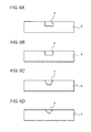
- the sectional shape of the groove portion 8 is a semicircular shape in the embodiment described above, it is not limited to such a shape. That is, as illustrated in Figs. 6A to 6D , various shapes can be adopted.
- Fig. 6A an upper portion and a lower portion have the same width.
- Fig. 6B the upper portion and the lower portion have the same width and edges of the bottom are rounded to have a circular-arc shape (R).
- the groove portion has a cross section of a trapezoidal shape where an area of an opening gradually increases as it approaches the upper surface.
- the groove portion has a cross section of an almost triangular shape where the area of the opening gradually increases as it approaches the upper surface.
- the groove portion 8 is formed in a rectangular shape which conforms the outer edge of the semiconductor chip 12, but the shape of the groove portion 8 needs not be limited thereto.
- the shapes illustrated in Figs. 7A to 7E can be adopted.
- the groove portion 8 has a double structure.
- the groove portion 8 can also have a triple structure.
- expanded portions 8a having a larger volume are formed in corners of the groove portion 8.
- Fig. 7B illustrates the expanded portion of a rectangular shape
- Fig. 7D illustrates the expanded portion of a circular shape.
- auxiliary groove portions 8b are additionally formed outside corners of the groove portion 8, respectively.
- the volume of the groove portion 8 is increased in a portion on which the molten solder tends to easily collect. Accordingly, these examples are advantageous in a point that it is possible to more surely prevent solder from spreading to the surroundings.
- Fig. 7A the groove portion 8 has a double structure.
- the groove portion 8 can also have a triple structure.
- expanded portions 8a having a larger volume are formed in corners of the groove portion 8.
- Fig. 7B illustrates the expanded portion of a rectangular shape
- Fig. 7D illustrates the expanded portion of a circular shape.
- auxiliary groove portions 8b are additionally formed outside corners
- the groove portion 8 does not have linear sides but has meandering sides. These meandering sides need not be regular in pattern. Various patterns like a pattern in which large curves and small curves are alternately arranged, a pattern made up of zigzag lines, etc. can be adopted. According to Fig. 7E and its similar configurations, it is possible to increase the volume of the groove portion 8 per unit area, and hence an effect of retaining molten solder can be exhibited.
- the groove portion 8 is not necessarily be formed in a continuous closed shape although the groove portions 8 of the examples have a continuous closed shape without any discontinuity. As illustrated in Figs. 8A to 8C , the groove portion 8 may have a discontinuous shape.
- each of four sides of the groove portion 8 has discontinuity in the middle and the auxiliary groove portions 8b of a straight line shape are formed outside position of discontinuity of the groove portion 8, respectively.
- Fig. 8B there is discontinuity in each of four corners of the groove portion 8 and the auxiliary groove portions 8b of an arc shape are formed outside positions of the discontinuity of the groove portion 8, respectively.
- Fig. 8C the groove portion 8 is formed with a double dotted line including an inside dotted line and an outside dotted line.
- the groove portion functions to increase a space volume, the space may not experience high pressure which leads to the explosion. Accordingly, scattering of the solder balls can be surely prevented. Furthermore, when the molten solder tries to spread into surroundings, the molten solder flows into the groove portion, and the flow of the molten solder beyond the groove portion is prevented. Therefore, the misalignment of the semiconductor chip to be mounted is prevented and the semiconductor can be guided to a desired position.
Landscapes
- Engineering & Computer Science (AREA)
- Microelectronics & Electronic Packaging (AREA)
- Electric Connection Of Electric Components To Printed Circuits (AREA)
Abstract
Description
- The present invention relates to a substrate structure to be used for reflow soldering.
- When mounting a semiconductor chip on a substrate using a reflow soldering method, solder paste is used. When an amount of printed solder paste is excessive or when a force of pushing a semiconductor chip is excessively strong, the solder paste overflows from a soldered surface of the semiconductor chip and is subjected to reflow heating. This leads to formation of solder balls or uncontrollable spreading of molten solder paste to a flow area.
- To deal with solder ball formation and uncontrollable spreading of molten solder paste to the flow area, conventionally, a buildup layer via-hole is provided so as to be connected to a pad on a printed circuit board, and a portion of copper plating inside the via-hole is removed to partially expose resin which is formed underneath the copper plating. This leads to forming of a via-hole inner wall portion where the resin is partially exposed. One such implementation is disclosed in Japanese Unexamined Patent Publication No.
2000-307224 - However, since the conventional substrate structure is constructed so that the molten solder is drained to the inside of the via-hole which is a closed space, there is a fear that flux evaporates and increases pressure in the closed space, which causes explosion. As a result, there is also a possibility that solder balls scatter circumferentially and the semiconductor chip cannot be mounted in a desired state.
- Furthermore, the conventional substrate structure is only for use in printed circuit boards, and cannot be used for a substrate where a semiconductor chip is mounted in a state in which the whole bottom surface of the semiconductor chip is in area contact with a copper plate formed in an upper surface of a substrate via solder paste. For this reason, there is no space to form a via-hole at all in the substrate.
- The object of the invention is to provide a substrate structure to be used during reflow soldering.
- In accordance with one aspect of the present invention, a substrate structure is configured to mount a semiconductor chip on a substrate by using a solder paste, the substrate includes a groove portion continuously or discontinuously surrounds the solder paste.
- The groove portion is preferably formed within an area occupied by the semiconductor chip to be mounted.
- In an alternate embodiment, the groove portion is preferably formed so that the width of an opening of the groove portion in a surface of the substrate is larger than a depth of the groove portion.
- The groove portion may have a depth equal to or less than 1/2 of a thickness of the substrate.
- The groove portion is preferably formed so that a total volume of the groove portion within the substrate is larger than a volume of flux to be evaporated when the solder paste melts.
- In one embodiment of the substrate structure, the groove portion is preferably formed so that a volume of a portion of the groove portion, corresponding to a corner of the semiconductor chip to be mounted is larger than any other portions.
- In one embodiment, the substrate is a DCB substrate (Direct Copper Bonding substrate) or a DBC substrate (Direct Bonding Copper substrate).
- In accordance with another aspect of the present invention, a method of mounting a semiconductor chip includes obtaining a mounting area by forming a groove portion, configuring the mounting area to continuously or discontinuously surround a predetermined area in the substrate, applying solder paste to a mounting area of the substrate, arranging the semiconductor chip on the solder paste, and bonding the semiconductor chip to the substrate using a reflow soldering process.
-
-
Fig. 1 is a perspective view illustrating a state in which a solid state relay according to one embodiment is viewed from the bottom side; -
Fig. 2 is a perspective view of a substrate which is embedded in the solid state relay ofFig. 1 ; -
Fig. 3 is an exploded perspective view of the substrate which is embedded in the solid state relay ofFig. 1 ; -
Fig. 4 is a perspective view showing a state after the substrate which is embedded in the solid straight relay ofFig. 1 is assembled; -
Figs. 5A is a schematic cross-sectional views of a substrate and a copper plate, illustrating a state before solder paste ofFig. 4 starts melting; -
Figs. 5B is a schematic cross-sectional views of a substrate and a copper plate, illustrating a after melting is started; -
Figs. 5C is a schematic cross-sectional views of a substrate and a copper plate, a state in which melting is completed; -
Figs. 6A to 6D are partial cross-sectional views each showing a copper plate portion of a substrate according to another embodiment; -
Figs. 7A to 7E are plan views each showing an example of a pattern of a groove portion (with no discontinuity) formed in a copper plate portion of a substrate according to another embodiment; and -
Figs. 8A to 8C are plan views each showing an example of a pattern of a groove portion (with discontinuity) formed in a copper plate portion of a substrate according to still another embodiment. - Hereinafter, embodiments of the present invention will be described with reference to the accompanying drawings. Moreover, terms (for example, terms including "upper," "lower," "side," and "end.") expressing specific directions and positions are used if necessary in the following description, but these terms are used only for an easy understanding of the present invention that is described with reference to the drawings and the meanings of these terms do not limit a technical scope of the present invention. Furthermore, the following description is only an example in nature, and is not intended to limit the present invention, applications thereof, or uses thereof.
-
Fig. 1 is a perspective view of a state in which an electronic device (solid state relay) incorporating therein a substrate 3 having a substrate structure according to the present embodiment is viewed from the bottom.Fig. 1 illustrates acasing 1 of an approximately rectangular parallelepiped which is open in the bottom surface (upper surface in the drawing), a plate-like base 2 which closes the bottom of thecasing 1, and four terminals (signal terminals 9 and 15 andpower terminals 10 and 13) protruding from the base 2. - As illustrated in
Fig. 2 , the substrate 3 is accommodated in thecasing 1. A DCB substrate (Direct Copper Bonding substrate) or a DBC substrate (Direct Bonding Copper substrate) is used as the substrate 3. A copper plate is directly joined with an upper surface of the substrate so as to form aconductive portion 4. Theconductive portion 4 includes a firstconductive portion 5, a secondconductive portion 6, and a thirdconductive portion 7. - The first
conductive portion 5 has a rectangular shape in a plan view, has arectangular groove portion 8 in an upper surface thereof, and as illustrated inFig. 3 , is connected to the first signal terminal 9 and thefirst power terminal 10. A Solder paste 11 (refer toFig. 5A ) is applied to an area surrounded by thegroove portion 8 using a printing method. - As illustrated in
Fig. 5A , thegroove portion 8 is formed along an outer edge of the mountedsemiconductor chip 12, and in a position inside the outer edge of thesemiconductor chip 12. Thegroove portion 8 has a semicircular cross-section, and has a depth which is equal to or less than a half of a thickness of the copper plate which constitutes the firstconductive portion 5. This leads to expansion of solder attributable to evaporation of flux, and thus flow of molten solder can be prevented while a decrease in an electric capacitance of a copper plate portion can be suppressed. A total volume of thegroove portion 8 within the substrate 3 is preferably larger than a volume offlux 11a which evaporates while thesemiconductor chip 12 is being soldered onto thesolder paste 11 as described below. Even though the flux evaporates and the volume of solder increases, since expansion of the volume of solder can be buffered, production of solder balls and scattering of the solder balls to surroundings which are attributable to explosion can be surely prevented. Therefore, problems such as a short circuit attributable to the spattered solder balls can be surely prevented Furthermore, thegroove portion 8 preferably has a volume at which themolten solder paste 11 can be retained and the flow of molten solder to the outside of thegroove portion 8 can be prevented. - The
semiconductor chip 12 is placed on thesolder paste 11. Thesemiconductor chip 12 is a conventionally known semiconductor chip and is configured such that when a voltage is applied from both input terminals, a photo diode embedded therein emits light, a triac switch turns on, and an electric current flows between output terminals. Thefirst power terminal 10 is connected to one input terminal, and thesecond power terminal 13 is connected to the other input terminal. The first signal terminal 9 is connected to one output terminal, and thesecond signal terminal 15 is connected to the other output terminal. - The
second power terminal 13 and anelectrode body 14 are connected to the secondconductive portion 6. Theelectrode body 14 is also connected to the input terminal on one side of thesemiconductor chip 12 so that thesemiconductor chip 12 can be applied with a voltage. Thesecond signal terminal 15 is connected to the thirdconductive portion 7. The thirdconductive portion 7 and the input terminal on the other side are connected to each other via asignal line 16. - Next, a method of manufacturing a solid state relay constructed in the way described above is described. A
groove portion 8 of a rectangular shape is formed in a firstconductive portion 5 of the substrate 3. Then,solder paste 11 is applied to an area surrounded by thegroove portion 8 using a printing method. Then, thesemiconductor chip 12 is placed on the appliedsolder paste 11. Each terminal is placed on aconductive portion 4 via thesolder paste 11,signal lines 16 are connected, and the connection is performed through reflow soldering. - During the reflow soldering, the
solder paste 11 between the substrate 3 and thesemiconductor chip 12 melts and flux evaporates. In this case, there is a fear that flux, which evaporates, increases pressure in a narrow space between the substrate 3 and thesemiconductor chip 12, causing explosion and producing solder balls. However, since thegroove portion 8 is formed, a sufficiently large space is provided. Therefore, as illustrated inFig. 5B , a phenomenon that the pressure in this area is increased by the evaporated flux is appropriately prevented, and therefore there is no fear that solder balls are produced by explosion. - For example, by setting a volume of the space in the
groove portion 8 to be larger than a volume of theflux 11a that evaporates, production of solder balls attributable to explosion can be surely prevented. - Furthermore, a volume of the space in the
groove portion 8 is preferably a volume at which thesolder paste 11 which is melted can be retained so as to prevent thesolder paste 11 from flowing outside beyond the groove portion. In this case, as illustrated inFig. 5C , thegroove portion 8 prevents themolten solder paste 11 from spreading to the surroundings thereof. That is, the area occupied by thesolder paste 11 is restricted to be within the area surrounded by thegroove portion 8. As a result, a mounting position of thesemiconductor chip 12 is not changed by melting of thesolder paste 11, and thesemiconductor chip 12 can be mounted in a desired position. - When the
groove portion 8 is formed along with an outer edge of thesemiconductor chip 12 placed on the substrate 3 and a portion of thegroove portion 8 is formed inside the outer edge of thesemiconductor chip 12, it is possible to surely prevent the molten solder from spreading to the outside of a mounting area of thesemiconductor chip 12. Particularly when a position of an outer edge of thegroove portion 8 is located inside a position of the outer edge of thesemiconductor chip 12, it is possible to prevent a short circuit attributable to solder adhering to a side surface of thesemiconductor chip 12. Hence, the alignment of the semiconductor chip can be more accurately performed. - Furthermore, when the
groove portion 8 has a semicircular cross section, a width of an opening of thegroove portion 8 in the surface of the substrate 3 is allowed to be larger than a depth of thegroove portion 8. With this configuration, since the molten solder can be smoothly flown into the groove portion, it is possible to secure a sufficient space volume of thegroove portion 8, thereby surely preventing the flow of the molten solder. In addition, since there is no need to secure a large depth of thegroove portion 8, it is possible to suppress the electric capacitance of the copper plate portion from decreasing. Still furthermore, when the depth of thegroove portion 8 is equal to or less than a half of the thickness of the copper plate that constitutes the firstconductive portion 5, it is possible to increase the space volume of thegroove portion 8 while suppressing a decrease in the electric capacitance of the copper plate portion. - Furthermore, the present invention is not limited to the configurations of the embodiments described above, and various modifications thereto are possible.
- For example, although the sectional shape of the
groove portion 8 is a semicircular shape in the embodiment described above, it is not limited to such a shape. That is, as illustrated inFigs. 6A to 6D , various shapes can be adopted. InFig. 6A , an upper portion and a lower portion have the same width. InFig. 6B , the upper portion and the lower portion have the same width and edges of the bottom are rounded to have a circular-arc shape (R). InFig. 6C , the groove portion has a cross section of a trapezoidal shape where an area of an opening gradually increases as it approaches the upper surface. InFig. 6D , the groove portion has a cross section of an almost triangular shape where the area of the opening gradually increases as it approaches the upper surface. - In addition, although the
groove portion 8 is formed in a rectangular shape which conforms the outer edge of thesemiconductor chip 12, but the shape of thegroove portion 8 needs not be limited thereto. The shapes illustrated inFigs. 7A to 7E can be adopted. - In
Fig. 7A , thegroove portion 8 has a double structure. Thegroove portion 8 can also have a triple structure. InFigs. 7B and 7C , expandedportions 8a having a larger volume are formed in corners of thegroove portion 8.Fig. 7B illustrates the expanded portion of a rectangular shape andFig. 7D illustrates the expanded portion of a circular shape. InFig. 7D ,auxiliary groove portions 8b are additionally formed outside corners of thegroove portion 8, respectively. According toFigs. 7B to 7D , the volume of thegroove portion 8 is increased in a portion on which the molten solder tends to easily collect. Accordingly, these examples are advantageous in a point that it is possible to more surely prevent solder from spreading to the surroundings. InFig. 7E , thegroove portion 8 does not have linear sides but has meandering sides. These meandering sides need not be regular in pattern. Various patterns like a pattern in which large curves and small curves are alternately arranged, a pattern made up of zigzag lines, etc. can be adopted. According toFig. 7E and its similar configurations, it is possible to increase the volume of thegroove portion 8 per unit area, and hence an effect of retaining molten solder can be exhibited. - The
groove portion 8 is not necessarily be formed in a continuous closed shape although thegroove portions 8 of the examples have a continuous closed shape without any discontinuity. As illustrated inFigs. 8A to 8C , thegroove portion 8 may have a discontinuous shape. - In
Fig. 8A , each of four sides of thegroove portion 8 has discontinuity in the middle and theauxiliary groove portions 8b of a straight line shape are formed outside position of discontinuity of thegroove portion 8, respectively, InFig. 8B , there is discontinuity in each of four corners of thegroove portion 8 and theauxiliary groove portions 8b of an arc shape are formed outside positions of the discontinuity of thegroove portion 8, respectively. InFig. 8C , thegroove portion 8 is formed with a double dotted line including an inside dotted line and an outside dotted line. - Thus, even using the
groove portion 8 having discontinuity, the flow of the molten solder can be prevented by theauxiliary groove portions 8b, etc. - As per the current invention, even though the solder melts during the reflow soldering and the flux evaporates, since the groove portion functions to increase a space volume, the space may not experience high pressure which leads to the explosion. Accordingly, scattering of the solder balls can be surely prevented. Furthermore, when the molten solder tries to spread into surroundings, the molten solder flows into the groove portion, and the flow of the molten solder beyond the groove portion is prevented. Therefore, the misalignment of the semiconductor chip to be mounted is prevented and the semiconductor can be guided to a desired position.
- There has thus been shown and described substrate structure and solid state relay which fulfills all the objects and advantages sought therefore. Many changes, modifications, variations and other uses and applications of the subject invention will, however, become apparent to those slcilled in the art after considering this specification and the accompanying drawings which disclose the preferred embodiments thereof. All such changes, modifications, variations and other uses and applications which do not depart from the spirit and scope of the invention are deemed to be covered by the invention, which is to be limited only by the claims which follow.
- Although the invention has been described in detail for the purpose of illustration based on what is currently considered to be the most practical and preferred embodiments, it is to be understood that such detail is solely for that purpose and that the invention is not limited to the disclosed embodiments, but, on the contrary, is intended to cover modifications and equivalent arrangements that are within the spirit and scope of the appended claims. For example, it is to be understood that the present invention contemplates that, to the extent possible, one or more features of any embodiment can be combined with one or more features of any other embodiment.
Claims (9)
- A substrate structure comprising:a substrate (3);a groove portion (8) on said substrate (3) for surrounding a solder paste (11), said groove portion (8) and solder paste (11) for mounting a semiconductor device.
- The substrate structure according to claim 1, wherein the groove portion (8) is formed within an area of the substrate (3) to be occupied by the semiconductor chip.
- The substrate structure according to claims 1 or 2, wherein a width of an opening in a surface of the substrate (3) is larger than a depth of the groove portion (8).
- The substrate structure according to any one of claims 1 to 3, wherein the groove portion (8) has a depth equal to or less than 1/2 of a thickness of the substrate.
- The substrate structure according to any one of claims 1 to 4, wherein a total volume of the groove portion (8) in the substrate is larger than a volume of flux to be evaporated when the solder paste (11) melts.
- The substrate structure according to any one of claims 1 to 5, wherein a volume of a portion of the groove portion (8) which corresponds to a corner of the semiconductor chip to be mounted is larger than any other portions.
- The substrate structure according to any one of claims 1 to 6, wherein the substrate (3) is a Direct Copper Bonding substrate or a Direct Bonding Copper substrate.
- A method of mounting a semiconductor chip, the method comprising:forming a groove portion (8) on a substrate (3) as a mounting area; configuring the mounting area to continuously or discontinuously surround a predetermined area in the substrate (3);applying solder paste (11) to the mounting area of the substrate (3);arranging the semiconductor chip on the solder paste (11); andbonding the semiconductor chip to the substrate (3) using a reflow soldering process.
- A solid state relay in which a substrate having the substrate structure according to any one of claims 1 to 7 is embedded.
Applications Claiming Priority (1)
| Application Number | Priority Date | Filing Date | Title |
|---|---|---|---|
| JP2012203236A JP2014060211A (en) | 2012-09-14 | 2012-09-14 | Substrate structure, semiconductor chip mounting method and solid state relay |
Publications (1)
| Publication Number | Publication Date |
|---|---|
| EP2709430A1 true EP2709430A1 (en) | 2014-03-19 |
Family
ID=48877110
Family Applications (1)
| Application Number | Title | Priority Date | Filing Date |
|---|---|---|---|
| EP20130178338 Withdrawn EP2709430A1 (en) | 2012-09-14 | 2013-07-29 | Substrate structure, method of mounting semiconductor chip, and solid state realy |
Country Status (4)
| Country | Link |
|---|---|
| US (1) | US9245829B2 (en) |
| EP (1) | EP2709430A1 (en) |
| JP (1) | JP2014060211A (en) |
| CN (1) | CN103687302B (en) |
Families Citing this family (10)
| Publication number | Priority date | Publication date | Assignee | Title |
|---|---|---|---|---|
| JP6350364B2 (en) * | 2015-04-01 | 2018-07-04 | 株式会社デンソー | Connection structure |
| CN105356652A (en) * | 2015-12-03 | 2016-02-24 | 宜兴市贵鑫磁电高科技有限公司 | Voice coil motor provided with electric connection point avoidance slots |
| DE102017209065A1 (en) * | 2017-05-30 | 2018-12-06 | Osram Gmbh | LIGHTING DEVICE, HEADLIGHTS AND METHOD |
| WO2019167254A1 (en) * | 2018-03-02 | 2019-09-06 | 新電元工業株式会社 | Semiconductor device and method for producing semiconductor device |
| JP7230419B2 (en) | 2018-10-16 | 2023-03-01 | 富士電機株式会社 | Semiconductor device, method for manufacturing semiconductor device |
| CN109855658A (en) * | 2019-05-06 | 2019-06-07 | 微传智能科技(常州)有限公司 | Motor, encoder, magnetic degree sensor and preparation method thereof |
| CN111524871A (en) * | 2020-04-10 | 2020-08-11 | 湖南国芯半导体科技有限公司 | Power module |
| CN112367773A (en) * | 2020-10-28 | 2021-02-12 | 安徽瑞迪微电子有限公司 | DBC substrate and chip welding method |
| JP7580364B2 (en) * | 2021-11-18 | 2024-11-11 | 三菱電機株式会社 | Semiconductor device and method for manufacturing the same |
| CN114300369A (en) * | 2022-03-10 | 2022-04-08 | 绍兴中芯集成电路制造股份有限公司 | Manufacturing method of semiconductor packaging structure |
Citations (5)
| Publication number | Priority date | Publication date | Assignee | Title |
|---|---|---|---|---|
| JPH0637123A (en) * | 1992-07-15 | 1994-02-10 | Hitachi Ltd | Semiconductor device |
| JP2000307224A (en) | 1999-04-22 | 2000-11-02 | Nippon Avionics Co Ltd | Printed wiring board for solder ball measures |
| US20030073349A1 (en) * | 2001-10-16 | 2003-04-17 | Yazaki Corporation | Structure of joining chip part to bus bars |
| JP2006351926A (en) * | 2005-06-17 | 2006-12-28 | Auto Network Gijutsu Kenkyusho:Kk | Circuit boards, electronic components and electrical junction boxes |
| EP1986478A2 (en) * | 2007-04-25 | 2008-10-29 | Denso Corporation | Metal wiring plate |
Family Cites Families (22)
| Publication number | Priority date | Publication date | Assignee | Title |
|---|---|---|---|---|
| JPS53116263U (en) * | 1977-02-23 | 1978-09-16 | ||
| JPS5656652U (en) * | 1979-10-02 | 1981-05-16 | ||
| JPS6289141U (en) * | 1985-11-25 | 1987-06-08 | ||
| JPS6379651U (en) * | 1986-11-12 | 1988-05-26 | ||
| WO1991005368A1 (en) * | 1989-10-05 | 1991-04-18 | Digital Equipment Corporation | Die attach structure and method |
| JPH0637122A (en) * | 1992-07-15 | 1994-02-10 | Hitachi Ltd | Semiconductor device |
| JPH08186217A (en) * | 1994-12-28 | 1996-07-16 | Rohm Co Ltd | Semiconductor device |
| EP1025587A4 (en) * | 1997-07-21 | 2000-10-04 | Aguila Technologies Inc | BUMP SEMICONDUCTOR CHIP PACKAGE AND MANUFACTURING METHOD THEREOF |
| US6249053B1 (en) * | 1998-02-16 | 2001-06-19 | Sumitomo Metal (Smi) Electronics Devices Inc. | Chip package and method for manufacturing the same |
| TW472367B (en) * | 2000-12-12 | 2002-01-11 | Siliconware Precision Industries Co Ltd | Passive device pad design for avoiding solder pearls |
| JP2003133366A (en) * | 2001-10-25 | 2003-05-09 | Texas Instr Japan Ltd | Semiconductor device and manufacturing method thereof |
| JP2004119568A (en) * | 2002-09-25 | 2004-04-15 | Kyocera Corp | Ceramic circuit board |
| TWI229928B (en) * | 2003-08-19 | 2005-03-21 | Advanced Semiconductor Eng | Semiconductor package structure |
| US20070026575A1 (en) * | 2005-06-24 | 2007-02-01 | Subramanian Sankara J | No flow underfill device and method |
| JP4738983B2 (en) * | 2005-11-08 | 2011-08-03 | ローム株式会社 | Semiconductor device |
| JP2007165600A (en) * | 2005-12-14 | 2007-06-28 | Omron Corp | Power module structure and solid state relay using the same |
| DE102006028675B4 (en) * | 2006-06-22 | 2008-08-21 | Siemens Ag | Cooling arrangement for arranged on a support plate electrical components |
| US7652374B2 (en) * | 2006-07-31 | 2010-01-26 | Chi Wah Kok | Substrate and process for semiconductor flip chip package |
| KR100840790B1 (en) * | 2006-11-29 | 2008-06-23 | 삼성전자주식회사 | Semiconductor module and manufacturing method thereof |
| JP5533619B2 (en) * | 2010-12-14 | 2014-06-25 | 株式会社デンソー | Semiconductor device |
| JP2013254870A (en) * | 2012-06-07 | 2013-12-19 | Fujitsu Ltd | Printed wiring board and solder method |
| CN103632988B (en) * | 2012-08-28 | 2016-10-19 | 宏启胜精密电子(秦皇岛)有限公司 | Package-on-package structure and preparation method thereof |
-
2012
- 2012-09-14 JP JP2012203236A patent/JP2014060211A/en active Pending
-
2013
- 2013-07-23 US US13/949,206 patent/US9245829B2/en active Active
- 2013-07-29 EP EP20130178338 patent/EP2709430A1/en not_active Withdrawn
- 2013-07-31 CN CN201310328762.XA patent/CN103687302B/en active Active
Patent Citations (5)
| Publication number | Priority date | Publication date | Assignee | Title |
|---|---|---|---|---|
| JPH0637123A (en) * | 1992-07-15 | 1994-02-10 | Hitachi Ltd | Semiconductor device |
| JP2000307224A (en) | 1999-04-22 | 2000-11-02 | Nippon Avionics Co Ltd | Printed wiring board for solder ball measures |
| US20030073349A1 (en) * | 2001-10-16 | 2003-04-17 | Yazaki Corporation | Structure of joining chip part to bus bars |
| JP2006351926A (en) * | 2005-06-17 | 2006-12-28 | Auto Network Gijutsu Kenkyusho:Kk | Circuit boards, electronic components and electrical junction boxes |
| EP1986478A2 (en) * | 2007-04-25 | 2008-10-29 | Denso Corporation | Metal wiring plate |
Also Published As
| Publication number | Publication date |
|---|---|
| JP2014060211A (en) | 2014-04-03 |
| US20140077375A1 (en) | 2014-03-20 |
| CN103687302B (en) | 2017-05-17 |
| US9245829B2 (en) | 2016-01-26 |
| CN103687302A (en) | 2014-03-26 |
Similar Documents
| Publication | Publication Date | Title |
|---|---|---|
| US9245829B2 (en) | Substrate structure, method of mounting semiconductor chip, and solid state relay | |
| JP2009016451A (en) | Connection structure between printed circuit board and electronic components | |
| EP1740029A1 (en) | Circuit substrate | |
| JP6570728B2 (en) | Electronic device and manufacturing method thereof | |
| US20110094788A1 (en) | Printed circuit board with insulating areas | |
| US7368666B2 (en) | Surface-mounting type electronic circuit unit without detachment of solder | |
| JP2013073989A (en) | Surface mounting passive element component, component carrier tape, wiring board with built-in component | |
| JP2011100912A (en) | Mounting structure of power semiconductor module on printed wiring board | |
| US8453917B1 (en) | Wave soldering of surface-mounting electronic devices on printed circuit board | |
| JP5500373B2 (en) | Manufacturing method of terminal connection | |
| JP2007088020A (en) | Circuit structure | |
| WO2023162578A1 (en) | Circuit substrate and method for mounting electronic component | |
| US20090080170A1 (en) | Electronic carrier board | |
| US20110174525A1 (en) | Method and Electronic Assembly to Attach a Component to a Substrate | |
| JP3928152B2 (en) | Printed wiring board | |
| JP2004235232A (en) | Electronic component mounting structure | |
| KR101141587B1 (en) | Block type pin for solder ball | |
| JP2004221415A (en) | Semiconductor package mounting structure | |
| JP4950581B2 (en) | Circuit module | |
| JP7597037B2 (en) | Substrate for mounting electronic components, electronic component mounting body and manufacturing method thereof, and electronic device | |
| US20160374204A1 (en) | Circuit board, electronic apparatus comprising circuit board, and method for soldering components | |
| JP2002374060A (en) | Electronic circuit board | |
| JP2004079872A (en) | Soldering structure for electronic circuit unit | |
| JP2005072482A (en) | Land pattern structure and electric component mounting board | |
| JP2023137600A (en) | Print circuit board |
Legal Events
| Date | Code | Title | Description |
|---|---|---|---|
| PUAI | Public reference made under article 153(3) epc to a published international application that has entered the european phase |
Free format text: ORIGINAL CODE: 0009012 |
|
| AK | Designated contracting states |
Kind code of ref document: A1 Designated state(s): AL AT BE BG CH CY CZ DE DK EE ES FI FR GB GR HR HU IE IS IT LI LT LU LV MC MK MT NL NO PL PT RO RS SE SI SK SM TR |
|
| AX | Request for extension of the european patent |
Extension state: BA ME |
|
| 17P | Request for examination filed |
Effective date: 20140911 |
|
| RBV | Designated contracting states (corrected) |
Designated state(s): AL AT BE BG CH CY CZ DE DK EE ES FI FR GB GR HR HU IE IS IT LI LT LU LV MC MK MT NL NO PL PT RO RS SE SI SK SM TR |
|
| 17Q | First examination report despatched |
Effective date: 20160729 |
|
| STAA | Information on the status of an ep patent application or granted ep patent |
Free format text: STATUS: EXAMINATION IS IN PROGRESS |
|
| STAA | Information on the status of an ep patent application or granted ep patent |
Free format text: STATUS: THE APPLICATION IS DEEMED TO BE WITHDRAWN |
|
| 18D | Application deemed to be withdrawn |
Effective date: 20191204 |