EP2709149A1 - Semiconductor device and manufacturing method thereof - Google Patents
Semiconductor device and manufacturing method thereof Download PDFInfo
- Publication number
- EP2709149A1 EP2709149A1 EP12786707.5A EP12786707A EP2709149A1 EP 2709149 A1 EP2709149 A1 EP 2709149A1 EP 12786707 A EP12786707 A EP 12786707A EP 2709149 A1 EP2709149 A1 EP 2709149A1
- Authority
- EP
- European Patent Office
- Prior art keywords
- insulating substrate
- heat
- base member
- conductor pattern
- semiconductor device
- Prior art date
- Legal status (The legal status is an assumption and is not a legal conclusion. Google has not performed a legal analysis and makes no representation as to the accuracy of the status listed.)
- Withdrawn
Links
Images






Classifications
-
- H—ELECTRICITY
- H10—SEMICONDUCTOR DEVICES; ELECTRIC SOLID-STATE DEVICES NOT OTHERWISE PROVIDED FOR
- H10W—GENERIC PACKAGES, INTERCONNECTIONS, CONNECTORS OR OTHER CONSTRUCTIONAL DETAILS OF DEVICES COVERED BY CLASS H10
- H10W70/00—Package substrates; Interposers; Redistribution layers [RDL]
- H10W70/40—Leadframes
- H10W70/461—Leadframes specially adapted for cooling
-
- H—ELECTRICITY
- H10—SEMICONDUCTOR DEVICES; ELECTRIC SOLID-STATE DEVICES NOT OTHERWISE PROVIDED FOR
- H10W—GENERIC PACKAGES, INTERCONNECTIONS, CONNECTORS OR OTHER CONSTRUCTIONAL DETAILS OF DEVICES COVERED BY CLASS H10
- H10W40/00—Arrangements for thermal protection or thermal control
- H10W40/70—Fillings or auxiliary members in containers or in encapsulations for thermal protection or control
- H10W40/77—Auxiliary members characterised by their shape
- H10W40/778—Auxiliary members characterised by their shape in encapsulations
-
- H—ELECTRICITY
- H10—SEMICONDUCTOR DEVICES; ELECTRIC SOLID-STATE DEVICES NOT OTHERWISE PROVIDED FOR
- H10W—GENERIC PACKAGES, INTERCONNECTIONS, CONNECTORS OR OTHER CONSTRUCTIONAL DETAILS OF DEVICES COVERED BY CLASS H10
- H10W40/00—Arrangements for thermal protection or thermal control
- H10W40/10—Arrangements for heating
-
- H—ELECTRICITY
- H10—SEMICONDUCTOR DEVICES; ELECTRIC SOLID-STATE DEVICES NOT OTHERWISE PROVIDED FOR
- H10W—GENERIC PACKAGES, INTERCONNECTIONS, CONNECTORS OR OTHER CONSTRUCTIONAL DETAILS OF DEVICES COVERED BY CLASS H10
- H10W42/00—Arrangements for protection of devices
- H10W42/121—Arrangements for protection of devices protecting against mechanical damage
-
- H—ELECTRICITY
- H10—SEMICONDUCTOR DEVICES; ELECTRIC SOLID-STATE DEVICES NOT OTHERWISE PROVIDED FOR
- H10W—GENERIC PACKAGES, INTERCONNECTIONS, CONNECTORS OR OTHER CONSTRUCTIONAL DETAILS OF DEVICES COVERED BY CLASS H10
- H10W70/00—Package substrates; Interposers; Redistribution layers [RDL]
- H10W70/60—Insulating or insulated package substrates; Interposers; Redistribution layers
- H10W70/62—Insulating or insulated package substrates; Interposers; Redistribution layers characterised by their interconnections
- H10W70/65—Shapes or dispositions of interconnections
- H10W70/658—Shapes or dispositions of interconnections for devices provided for in groups H10D8/00 - H10D48/00
-
- H—ELECTRICITY
- H10—SEMICONDUCTOR DEVICES; ELECTRIC SOLID-STATE DEVICES NOT OTHERWISE PROVIDED FOR
- H10W—GENERIC PACKAGES, INTERCONNECTIONS, CONNECTORS OR OTHER CONSTRUCTIONAL DETAILS OF DEVICES COVERED BY CLASS H10
- H10W72/00—Interconnections or connectors in packages
- H10W72/071—Connecting or disconnecting
- H10W72/073—Connecting or disconnecting of die-attach connectors
-
- H—ELECTRICITY
- H10—SEMICONDUCTOR DEVICES; ELECTRIC SOLID-STATE DEVICES NOT OTHERWISE PROVIDED FOR
- H10W—GENERIC PACKAGES, INTERCONNECTIONS, CONNECTORS OR OTHER CONSTRUCTIONAL DETAILS OF DEVICES COVERED BY CLASS H10
- H10W72/00—Interconnections or connectors in packages
- H10W72/30—Die-attach connectors
-
- H—ELECTRICITY
- H10—SEMICONDUCTOR DEVICES; ELECTRIC SOLID-STATE DEVICES NOT OTHERWISE PROVIDED FOR
- H10W—GENERIC PACKAGES, INTERCONNECTIONS, CONNECTORS OR OTHER CONSTRUCTIONAL DETAILS OF DEVICES COVERED BY CLASS H10
- H10W72/00—Interconnections or connectors in packages
- H10W72/60—Strap connectors, e.g. thick copper clips for grounding of power devices
-
- H—ELECTRICITY
- H10—SEMICONDUCTOR DEVICES; ELECTRIC SOLID-STATE DEVICES NOT OTHERWISE PROVIDED FOR
- H10W—GENERIC PACKAGES, INTERCONNECTIONS, CONNECTORS OR OTHER CONSTRUCTIONAL DETAILS OF DEVICES COVERED BY CLASS H10
- H10W40/00—Arrangements for thermal protection or thermal control
- H10W40/20—Arrangements for cooling
- H10W40/25—Arrangements for cooling characterised by their materials
- H10W40/255—Arrangements for cooling characterised by their materials having a laminate or multilayered structure, e.g. direct bond copper [DBC] ceramic substrates
-
- H—ELECTRICITY
- H10—SEMICONDUCTOR DEVICES; ELECTRIC SOLID-STATE DEVICES NOT OTHERWISE PROVIDED FOR
- H10W—GENERIC PACKAGES, INTERCONNECTIONS, CONNECTORS OR OTHER CONSTRUCTIONAL DETAILS OF DEVICES COVERED BY CLASS H10
- H10W72/00—Interconnections or connectors in packages
- H10W72/071—Connecting or disconnecting
- H10W72/073—Connecting or disconnecting of die-attach connectors
- H10W72/07331—Connecting techniques
- H10W72/07336—Soldering or alloying
-
- H—ELECTRICITY
- H10—SEMICONDUCTOR DEVICES; ELECTRIC SOLID-STATE DEVICES NOT OTHERWISE PROVIDED FOR
- H10W—GENERIC PACKAGES, INTERCONNECTIONS, CONNECTORS OR OTHER CONSTRUCTIONAL DETAILS OF DEVICES COVERED BY CLASS H10
- H10W72/00—Interconnections or connectors in packages
- H10W72/071—Connecting or disconnecting
- H10W72/076—Connecting or disconnecting of strap connectors
-
- H—ELECTRICITY
- H10—SEMICONDUCTOR DEVICES; ELECTRIC SOLID-STATE DEVICES NOT OTHERWISE PROVIDED FOR
- H10W—GENERIC PACKAGES, INTERCONNECTIONS, CONNECTORS OR OTHER CONSTRUCTIONAL DETAILS OF DEVICES COVERED BY CLASS H10
- H10W72/00—Interconnections or connectors in packages
- H10W72/071—Connecting or disconnecting
- H10W72/076—Connecting or disconnecting of strap connectors
- H10W72/07631—Techniques
- H10W72/07632—Compression bonding, e.g. thermocompression bonding
- H10W72/07633—Ultrasonic bonding, e.g. thermosonic bonding
-
- H—ELECTRICITY
- H10—SEMICONDUCTOR DEVICES; ELECTRIC SOLID-STATE DEVICES NOT OTHERWISE PROVIDED FOR
- H10W—GENERIC PACKAGES, INTERCONNECTIONS, CONNECTORS OR OTHER CONSTRUCTIONAL DETAILS OF DEVICES COVERED BY CLASS H10
- H10W72/00—Interconnections or connectors in packages
- H10W72/071—Connecting or disconnecting
- H10W72/076—Connecting or disconnecting of strap connectors
- H10W72/07631—Techniques
- H10W72/07635—Applying EM radiation, e.g. induction heating or using a laser
-
- H—ELECTRICITY
- H10—SEMICONDUCTOR DEVICES; ELECTRIC SOLID-STATE DEVICES NOT OTHERWISE PROVIDED FOR
- H10W—GENERIC PACKAGES, INTERCONNECTIONS, CONNECTORS OR OTHER CONSTRUCTIONAL DETAILS OF DEVICES COVERED BY CLASS H10
- H10W72/00—Interconnections or connectors in packages
- H10W72/071—Connecting or disconnecting
- H10W72/076—Connecting or disconnecting of strap connectors
- H10W72/07631—Techniques
- H10W72/07636—Soldering or alloying
-
- H—ELECTRICITY
- H10—SEMICONDUCTOR DEVICES; ELECTRIC SOLID-STATE DEVICES NOT OTHERWISE PROVIDED FOR
- H10W—GENERIC PACKAGES, INTERCONNECTIONS, CONNECTORS OR OTHER CONSTRUCTIONAL DETAILS OF DEVICES COVERED BY CLASS H10
- H10W72/00—Interconnections or connectors in packages
- H10W72/071—Connecting or disconnecting
- H10W72/076—Connecting or disconnecting of strap connectors
- H10W72/07651—Connecting or disconnecting of strap connectors characterised by changes in properties of the strap connectors during connecting
- H10W72/07653—Connecting or disconnecting of strap connectors characterised by changes in properties of the strap connectors during connecting changes in shapes
-
- H—ELECTRICITY
- H10—SEMICONDUCTOR DEVICES; ELECTRIC SOLID-STATE DEVICES NOT OTHERWISE PROVIDED FOR
- H10W—GENERIC PACKAGES, INTERCONNECTIONS, CONNECTORS OR OTHER CONSTRUCTIONAL DETAILS OF DEVICES COVERED BY CLASS H10
- H10W72/00—Interconnections or connectors in packages
- H10W72/50—Bond wires
- H10W72/551—Materials of bond wires
- H10W72/552—Materials of bond wires comprising metals or metalloids, e.g. silver
- H10W72/5524—Materials of bond wires comprising metals or metalloids, e.g. silver comprising aluminium [Al]
-
- H—ELECTRICITY
- H10—SEMICONDUCTOR DEVICES; ELECTRIC SOLID-STATE DEVICES NOT OTHERWISE PROVIDED FOR
- H10W—GENERIC PACKAGES, INTERCONNECTIONS, CONNECTORS OR OTHER CONSTRUCTIONAL DETAILS OF DEVICES COVERED BY CLASS H10
- H10W72/00—Interconnections or connectors in packages
- H10W72/60—Strap connectors, e.g. thick copper clips for grounding of power devices
- H10W72/631—Shapes of strap connectors
-
- H—ELECTRICITY
- H10—SEMICONDUCTOR DEVICES; ELECTRIC SOLID-STATE DEVICES NOT OTHERWISE PROVIDED FOR
- H10W—GENERIC PACKAGES, INTERCONNECTIONS, CONNECTORS OR OTHER CONSTRUCTIONAL DETAILS OF DEVICES COVERED BY CLASS H10
- H10W72/00—Interconnections or connectors in packages
- H10W72/60—Strap connectors, e.g. thick copper clips for grounding of power devices
- H10W72/651—Materials of strap connectors
- H10W72/652—Materials of strap connectors comprising metals or metalloids, e.g. silver
-
- H—ELECTRICITY
- H10—SEMICONDUCTOR DEVICES; ELECTRIC SOLID-STATE DEVICES NOT OTHERWISE PROVIDED FOR
- H10W—GENERIC PACKAGES, INTERCONNECTIONS, CONNECTORS OR OTHER CONSTRUCTIONAL DETAILS OF DEVICES COVERED BY CLASS H10
- H10W72/00—Interconnections or connectors in packages
- H10W72/851—Dispositions of multiple connectors or interconnections
- H10W72/853—On the same surface
- H10W72/871—Bond wires and strap connectors
-
- H—ELECTRICITY
- H10—SEMICONDUCTOR DEVICES; ELECTRIC SOLID-STATE DEVICES NOT OTHERWISE PROVIDED FOR
- H10W—GENERIC PACKAGES, INTERCONNECTIONS, CONNECTORS OR OTHER CONSTRUCTIONAL DETAILS OF DEVICES COVERED BY CLASS H10
- H10W72/00—Interconnections or connectors in packages
- H10W72/851—Dispositions of multiple connectors or interconnections
- H10W72/874—On different surfaces
- H10W72/884—Die-attach connectors and bond wires
-
- H—ELECTRICITY
- H10—SEMICONDUCTOR DEVICES; ELECTRIC SOLID-STATE DEVICES NOT OTHERWISE PROVIDED FOR
- H10W—GENERIC PACKAGES, INTERCONNECTIONS, CONNECTORS OR OTHER CONSTRUCTIONAL DETAILS OF DEVICES COVERED BY CLASS H10
- H10W72/00—Interconnections or connectors in packages
- H10W72/90—Bond pads, in general
- H10W72/921—Structures or relative sizes of bond pads
- H10W72/926—Multiple bond pads having different sizes
-
- H—ELECTRICITY
- H10—SEMICONDUCTOR DEVICES; ELECTRIC SOLID-STATE DEVICES NOT OTHERWISE PROVIDED FOR
- H10W—GENERIC PACKAGES, INTERCONNECTIONS, CONNECTORS OR OTHER CONSTRUCTIONAL DETAILS OF DEVICES COVERED BY CLASS H10
- H10W74/00—Encapsulations, e.g. protective coatings
-
- H—ELECTRICITY
- H10—SEMICONDUCTOR DEVICES; ELECTRIC SOLID-STATE DEVICES NOT OTHERWISE PROVIDED FOR
- H10W—GENERIC PACKAGES, INTERCONNECTIONS, CONNECTORS OR OTHER CONSTRUCTIONAL DETAILS OF DEVICES COVERED BY CLASS H10
- H10W76/00—Containers; Fillings or auxiliary members therefor; Seals
- H10W76/40—Fillings or auxiliary members in containers, e.g. centering rings
- H10W76/42—Fillings
- H10W76/47—Solid or gel fillings
-
- H—ELECTRICITY
- H10—SEMICONDUCTOR DEVICES; ELECTRIC SOLID-STATE DEVICES NOT OTHERWISE PROVIDED FOR
- H10W—GENERIC PACKAGES, INTERCONNECTIONS, CONNECTORS OR OTHER CONSTRUCTIONAL DETAILS OF DEVICES COVERED BY CLASS H10
- H10W90/00—Package configurations
-
- H—ELECTRICITY
- H10—SEMICONDUCTOR DEVICES; ELECTRIC SOLID-STATE DEVICES NOT OTHERWISE PROVIDED FOR
- H10W—GENERIC PACKAGES, INTERCONNECTIONS, CONNECTORS OR OTHER CONSTRUCTIONAL DETAILS OF DEVICES COVERED BY CLASS H10
- H10W90/00—Package configurations
- H10W90/701—Package configurations characterised by the relative positions of pads or connectors relative to package parts
-
- H—ELECTRICITY
- H10—SEMICONDUCTOR DEVICES; ELECTRIC SOLID-STATE DEVICES NOT OTHERWISE PROVIDED FOR
- H10W—GENERIC PACKAGES, INTERCONNECTIONS, CONNECTORS OR OTHER CONSTRUCTIONAL DETAILS OF DEVICES COVERED BY CLASS H10
- H10W90/00—Package configurations
- H10W90/701—Package configurations characterised by the relative positions of pads or connectors relative to package parts
- H10W90/731—Package configurations characterised by the relative positions of pads or connectors relative to package parts of die-attach connectors
- H10W90/734—Package configurations characterised by the relative positions of pads or connectors relative to package parts of die-attach connectors between a chip and a stacked insulating package substrate, interposer or RDL
-
- H—ELECTRICITY
- H10—SEMICONDUCTOR DEVICES; ELECTRIC SOLID-STATE DEVICES NOT OTHERWISE PROVIDED FOR
- H10W—GENERIC PACKAGES, INTERCONNECTIONS, CONNECTORS OR OTHER CONSTRUCTIONAL DETAILS OF DEVICES COVERED BY CLASS H10
- H10W90/00—Package configurations
- H10W90/701—Package configurations characterised by the relative positions of pads or connectors relative to package parts
- H10W90/751—Package configurations characterised by the relative positions of pads or connectors relative to package parts of bond wires
- H10W90/754—Package configurations characterised by the relative positions of pads or connectors relative to package parts of bond wires between a chip and a stacked insulating package substrate, interposer or RDL
-
- H—ELECTRICITY
- H10—SEMICONDUCTOR DEVICES; ELECTRIC SOLID-STATE DEVICES NOT OTHERWISE PROVIDED FOR
- H10W—GENERIC PACKAGES, INTERCONNECTIONS, CONNECTORS OR OTHER CONSTRUCTIONAL DETAILS OF DEVICES COVERED BY CLASS H10
- H10W90/00—Package configurations
- H10W90/701—Package configurations characterised by the relative positions of pads or connectors relative to package parts
- H10W90/761—Package configurations characterised by the relative positions of pads or connectors relative to package parts of strap connectors
- H10W90/764—Package configurations characterised by the relative positions of pads or connectors relative to package parts of strap connectors between a chip and a stacked insulating package substrate, interposer or RDL
Definitions
- the present invention relates to a semiconductor device that is intended for, for example, a power semiconductor module and a method of manufacturing the same, and more particularly, to a semiconductor device having a connection structure in which a power semiconductor chip is mounted on an insulating substrate and the insulating substrate is bonded to a heat-dissipating base member such that heat generated from the power semiconductor chip can be dissipated to the outside and a method of manufacturing the same.
- the amount of current flowing through wiring lines in the package has increased and it is necessary to improve the radiation performance of the module.
- a lead frame using a copper plate is used, instead of aluminum wire bonding according to the related art, in order to reduce wiring inductance.
- Fig. 8 is a vertical cross-sectional view and a plan view illustrating a semiconductor device according to the related art.
- Fig. 8(A) is a vertical cross-sectional view taken along the line A-A of Fig. 8(B) .
- An insulating substrate 1 made of, for example, ceramic is a DBC (Direct Bonding Copper) substrate having conductor patterns 2a and 2b bonded to both surfaces thereof.
- a semiconductor chip 3 is mounted on the conductor pattern 2a which is formed as a copper circuit on the front surface of the insulating substrate 1 by soldering.
- DBC Direct Bonding Copper
- the conductor pattern 2b which has the same thickness as the conductor pattern 2a and is bonded to the rear surface of the insulating substrate 1 is bonded to a heat-dissipating base member 4 such that heat generated from the semiconductor chip 3 is dissipated to the outside.
- the heat-dissipating base member 4 forms the bottom of a resin case 5 and two large and small insulating substrates 1 are bonded to the heat-dissipating base member 4.
- the semiconductor chip 3, an internal connection terminal 7, and an aluminum wire 8 are protected by a gel-like sealing member 6 which is filled in the resin case 5.
- Fig. 8(B) is a plan view illustrating the state of the semiconductor device before the sealing member 6 is filled.
- Metal electrodes 3a and 3b of the semiconductor chip 3 are internally wired to predetermined portions of the conductor pattern 2a by the internal connection terminal 7 and the aluminum wire 8.
- a plurality of external lead terminals 9a and 9b are drawn from the conductor pattern 2a to the upper surface of the resin case 5.
- the internal connection terminal 7 and the external lead terminals 9a and 9b are lead frames obtained by processing copper plates.
- the metal electrodes 3a and 3b of the semiconductor chip 3 and the internal connection terminal 7 and also the internal connection terminal 7 and the conductor pattern 2a fixed to the insulating substrate 1 are wired inside the device, and the external lead terminals 9a and 9b are drawn to the outside of the device.
- the semiconductor chip 3 and the conductor pattern 2a, the conductor pattern 2b and the heat-dissipating base member 4, or the conductor pattern 2a and the internal connection terminal 7 or the external lead terminals 9a and 9b are connected to be wired by, for example, soldering, brazing, ultrasonic bonding, or laser welding.
- components of the semiconductor device have a square shape or a rectangular shape and are formed by bonding metal materials with different thermal expansion coefficients.
- Fig. 9 is a cross-sectional view illustrating the semiconductor device according to the related art taken along the line IX-IX of Fig. 8(A) .
- the conductor pattern 2b bonded to the heat-dissipating base member 4 has a square shape or a rectangular shape, as illustrated in Fig. 9 .
- each of the components which are connected to each other has a shape corresponding to the outer shape of the module and has a square shape or a rectangular shape.
- the components have different thermal expansion coefficients in, for example, the temperature cycle reliability test and stress which occurs along the bonding surface is concentrated on an angular corner. Therefore, a solder layer or a brazing filler metal layer is likely to be broken or cracked.
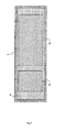
- Fig. 10 is a diagram illustrating a crack which occurs in a solder fixing layer in the temperature cycle test.
- Figs. 10(A) and 10(B) illustrate cracks which occur when components are repeatedly expanded and contracted in, for example, the temperature cycle reliability test in a state in which the conductor patterns 2b formed on the rear surfaces of the two large and small insulating substrates 1 illustrated in Fig. 8 are fixed to the heat-dissipating base member 4 by soldering.
- Figs. 10(A) and 10(B) the progression direction of the crack which occurs in each of the fixing layers 13a and 13b is represented by an arrow.
- a region corresponding to a portion of the solder in which a crack occurs is represented as a large white region.
- Patent Document 1 discloses a semiconductor device with the following connection structure.
- the thickness of a solder layer is small, fatigue breakdown occurs rapidly due to thermal stress which is applied to a soldering portion due to the difference in thermal expansion between an insulating substrate and a lead frame due to a heat cycle in a usage environment. Therefore, a protrusion is formed on a soldering surface of the copper circuit pattern of the lead frame or the insulating substrate to prevent a variation in the thickness of the solder layer.
- Patent Document 2 discloses a structure in which, in order to reduce stress applied to a bonding portion, chamfered portions are formed at four corners of a substrate or a slit is formed in a conductor pattern. In this structure, thermal stress which is applied to the bonding portion due to a thermal cycle is reduced to increase the time until a crack occurs, thereby preventing the growth of the crack.
- the invention has been made in view of the above-mentioned problems and an object of the invention is to provide a semiconductor device which is capable of reducing the concentration of stress on the corners of a bonding portion to suppress or prevent the progression of a crack in a solder layer in, for example, a temperature cycle reliability test and a method of manufacturing the same.
- a semiconductor device having a connection structure in which a power semiconductor chip is mounted on an insulating substrate having conductor patterns bonded to front and rear surfaces thereof and the insulating substrate is connected to a heat-dissipating base member such that heat generated from the power semiconductor chip can be dissipated to the outside.
- a bonding portion of the conductor pattern on the rear surface of the insulating substrate which is bonded to the heat-dissipating base member has a rectangular shape and has a predetermined curvature radius in the vicinity of corners. The predetermined curvature radius is in the range of 1 mm to 10 mm.
- a semiconductor device having a connection structure in which a power semiconductor chip is mounted on an insulating substrate having conductor patterns bonded to front and rear surfaces thereof and the insulating substrate is connected to a heat-dissipating base member such that heat generated from the power semiconductor chip can be dissipated to the outside.
- the conductor pattern on the rear surface of the insulating substrate which is bonded to the heat-dissipating base member includes a plurality of bonding portions to the corresponding heat-dissipating base member.
- Each of the plurality of bonding portions has a rectangular shape and has a predetermined curvature radius in the vicinity of corners. The predetermined curvature radius is in the range of 1 mm to 10 mm.
- a semiconductor device having a connection structure in which a power semiconductor chip is mounted on an insulating substrate having conductor patterns bonded to front and rear surfaces thereof and the insulating substrate is connected to a heat-dissipating base member such that heat generated from the power semiconductor chip can be dissipated to the outside.
- the conductor pattern on the rear surface of the insulating substrate which is bonded to the heat-dissipating base member includes a plurality of bonding portions to the corresponding heat-dissipating base member.
- Each of the plurality of bonding portions has a rectangular shape and has a predetermined curvature radius in the vicinity of corners. The predetermined curvature radius is in the range of 1 mm to 10 mm.
- a semiconductor device having a connection structure in which a power semiconductor chip is mounted on an insulating substrate having conductor patterns bonded to front and rear surfaces thereof and the insulating substrate is connected to a heat-dissipating base member such that heat generated from the power semiconductor chip can be dissipated to the outside.
- a bonding portion of the conductor pattern on the rear surface of the insulating substrate which is bonded to the heat-dissipating base member has a shape in which it includes one or more curved portions and has a predetermined curvature radius in the vicinity of the curved portions and corners.
- the predetermined curvature radius is in the range of 1 mm to 10 mm.
- a semiconductor device having a connection structure in which a power semiconductor chip is mounted on an insulating substrate having conductor patterns bonded to front and rear surfaces thereof and the insulating substrate is connected to a heat-dissipating base member such that heat generated from the power semiconductor chip can be dissipated to the outside.
- the conductor pattern on the rear surface of the insulating substrate which is bonded to the heat-dissipating base member includes a plurality of bonding portions to the corresponding heat-dissipating base member. Each of the plurality of bonding portions has a polygonal shape with six or more sides.
- the method includes: bonding conductor patterns to front and rear surfaces of the insulating substrate, a bonding portion of the conductor pattern on the rear surface of the insulating substrate having a rectangular shape and having a predetermined curvature radius in the vicinity of corners; providing sheet-shaped solder that has the same planar shape as the conductor pattern and has a predetermined thickness between the heat-dissipating base member and the conductor pattern; and solidifying the sheet-shaped solder to form a solder fixing layer that connects the conductor pattern to the heat-dissipating base member.
- the predetermined curvature radius is in the range of 1 mm to 10 mm.
- stress applied to the corners of the fixing layer is set to an elastic limit or less. In this way, it is possible to suppress and prevent the occurrence of a crack in the fixing layer. Therefore, the radiation performance of the semiconductor device which is used under harsh temperature conditions is ensured and it is possible to increase the lifespan of the semiconductor device.
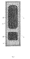
- Fig. 1 is a vertical cross-sectional view and a plan view illustrating a semiconductor device according to a first embodiment of the invention.
- Fig. 2 is a cross-sectional view taken along the line II-II of Fig. 1(A) .
- a semiconductor chip 3 is mounted on an insulating substrate 1 having conductor patterns 2a and 2b bonded to the front and rear surfaces thereof, and the insulating substrate 1 is bonded to a heat-dissipating base member 4. In this way, it is possible to dissipate heat generated from the semiconductor chip 3 to the outside.
- external lead terminals 9a and 9b which are lead frames of copper plates, are bonded to the conductor pattern 2a on the front surface of the insulating substrate 1 having the semiconductor chip 3 mounted thereon.
- the power semiconductor device includes an internal connection terminal 70 which connects a metal electrode 3a of the semiconductor chip 3 and the conductor pattern 2a.
- the connection structure is the same as that of the device according to the related art illustrated in Fig. 8 .
- the first characteristic of the power semiconductor device is that the outer shape of bonding portions 71, 72, and 91 of the internal connection terminal 70 and the external lead terminals 9a and 9b is a curved shape which is exemplified by a circular shape.
- the second characteristic thereof is that, as illustrated in Fig. 2 , the corners of the conductor pattern 2b bonded to the heat-dissipating base member 4 are rounded and the outline of the conductor pattern has a curved shape, which makes it possible to reduce the concentration of stress and prevent the occurrence of a crack in a solder fixing layer between the heat-dissipating base member 4. That is, as illustrated in Fig.
- a bonding portion of the conductor pattern 2b which is bonded to the heat-dissipating base member 4 on the rear surface side of the insulating substrate 1 has a rectangular shape and is slightly larger than the insulating substrate 1.
- the conductor pattern 2b has a predetermined curvature radius in the vicinity of the corners. The curvature radius may be experimentally in the range of 1 mm to 10 mm.
- the bonding portions 71 and 72 of the internal connection terminal 70 which has one end bonded to the conductor pattern 2a on the front surface of the insulating substrate on which the semiconductor chip 3 is mounted have a circular shape.
- the bonding portions 91 of the external lead terminal 9a and 9b which are drawn from the conductor pattern 2a on the front surface of the insulating substrate have a circular shape. In this way, the corners of the solder fixing layer are rounded and stress applied to the rounded corners can be set to an elastic limit or less. Therefore, the radiation performance of the semiconductor device is ensured.
- Fig. 3 is a cross-sectional view illustrating a state in which two metal members are bonded to each other by a solder fixing layer.
- the X-axis represents the length direction of the members and the Y-axis represents the thickness direction of the members.
- metal members 11 and 12 have different thermal expansion coefficients ⁇ 1 and ⁇ 2 ( ⁇ 1 ⁇ ⁇ 2) and have longitudinal elastic moduli E1 and E2, respectively.
- a fixing layer 13 is a solder layer with a shear elastic modulus Gc and has a thickness h.
- a solder fillet is formed in an outer circumferential portion of the fixing layer 13, with the second metal member 12 being bonded to the first metal member 11 through the solder fixing layer 13.
- the second metal member 12 with a length L and a thickness t2 is bonded to the first metal member 11 with a thickness t1 and the shear strain rate ( ⁇ ) of the solder of the fixing layer 13 when a temperature variation of T[°C] occurs in the bonded structure is calculated by the following Expression 1.
- the length L in Expression 1 is reduced since the shape of the bonding portions is a circle.
- the conductor pattern 2b which is bonded to the rear surface of the insulating substrate 1 has a rectangular bonding surface to the heat-dissipating base member 4 and the corner of the rectangular bonding surface has a predetermined curvature radius. Therefore, the length L in Expression 1 is reduced. In this way, it is possible to reduce the shear strain rate ⁇ acting on the fixing layer 13.
- the bonding portion of the conductor pattern to the rear surface of the insulating substrate 1 has a rectangular shape and the corners of the conductor pattern are rounded.
- sheet-shaped solder which has the same planar shape as the conductor pattern 2b and has a predetermined thickness is provided between the heat-dissipating base member 4 and the conductor pattern 2b and is heated. Then, the molten sheet-shaped solder is solidified to form a solder fixing layer which connects the conductor pattern 2b to the heat-dissipating base member 4.
- the conductor pattern 2b may be bonded to the heat-dissipating base member 4 by brazing.
- the conductor pattern 2b which is bonded to the heat-dissipating base member 4 is formed such that the thickness of a circumferential portion of the bonding surface to the insulating substrate 1 is less than that of the center of the bonding portion. In this way, it is possible to set stress applied to the solder fixing layer to an elastic limit or less. Therefore, the shear strain rate ⁇ acting on the fixing layer 13 illustrated in Fig. 3 is further reduced.
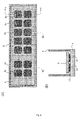
- Fig. 4 is a diagram illustrating a bonding state between a heat-dissipating base member and an insulating substrate of a semiconductor device according to a second embodiment of the invention.
- Conductor patterns including four and ten divided conductor layers 2c are provided on the rear surfaces of insulating substrates 1a and 1b which are bonded to the heat-dissipating base member 4, respectively.
- Each of the conductor layers 2c has a rectangular pattern shape with rounded corners. In this way, it is possible to reduce the size of a solder fixing layer 13 for fixing each conductor layer 2c to the heat-dissipating base member 4.
- the number of divided conductor layers 2c is not limited four or ten, but one insulating substrate may be divided into two or more conductor layers. In this case, the same effect as described above is obtained.
- Fig. 5 is a diagram illustrating a bonding state between a heat-dissipating base member and an insulating substrate of a semiconductor device according to a third embodiment of the invention.
- the power semiconductor device includes bonding portions 20 which protrude from a plurality of divided regions of a conductor pattern 2b on the rear surface of the insulating substrate bonded to a heat-dissipating base member 4 to the heat-dissipating base member 4. In this case, it is possible to reduce the size of a solder fixing layer 13 for fixing each of the bonding portions 20 to the heat-dissipating base member 4.
- Fig. 6 is a plan view and a vertical cross-sectional view illustrating a semiconductor device according to a fourth embodiment of the invention.
- a plurality of circular protruding portions 7f are formed on each of bonding portions 73a and 73b of an internal connection terminal 73.
- two circular protruding portions 9f are formed on each of bonding portions 91 of external lead terminals 9a and 9b.
- the circular protruding portions 7f and 9f are bonded to a metal electrode 3a and a conductor pattern 2a through an individual solder fixing layer 13. Therefore, the size of the solder fixing layer 13 is reduced and it is possible to reduce the shear strain rate ⁇ acting on the fixing layer 13.
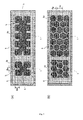
- Fig. 7 is a diagram illustrating a bonding state between a heat-dissipating base member and an insulating substrate of a semiconductor device according to a fifth embodiment of the invention.
- conductor patterns 2b which bond insulating substrates 1a and 1b to a heat-dissipating base member 4 have two different shapes.
- the conductor pattern 2b illustrated in Fig. 7(A) includes a rectangular bonding portion having a curvature radius r in the vicinity of the corner and a plurality of curved (bent) portions (bend) b with a concave shape are formed in each side of the bonding portion.
- the curvature radius r may be experimentally in the range of 1 mm to 10 mm.
- the width Bw of the curved portion b be equal to or greater than r and the depth Bd of the curved portion b be equal to or greater than r.
- the conductor pattern 2b illustrated in Fig. 7(A) is configured such that the length L of a straight portion of the second metal member 12 illustrated in Fig. 3 is reduced.
- the corner of the inside bottom of the curved portion have the same curvature radius as described above. According to this structure, it is possible to reduce the shear strain rate ⁇ of the corner.
- the conductor pattern illustrated in Fig. 7(B) includes a plurality of divided conductor layers 2d and has a hexagonal pattern shape or a trapezoidal pattern shape which forms a portion of the hexagonal shape.
- a gap Sg between the conductor layers 2d be equal to or greater than 0.1 ⁇ Sd.
- the shape of the plurality of divided conductor layers is not limited to a hexagon, but it may be a polygon having six or more sides.
- the polygon may be a regular polygon.
- the shape of the divided conductor layer is a polygon having six or more sides, it is possible to reduce the shear strain rate ⁇ at the corners.
- it is effective that an angular portion of the polygon has the above-mentioned curvature radius.
Landscapes
- Cooling Or The Like Of Semiconductors Or Solid State Devices (AREA)
Abstract
Provided is a semiconductor device and a method of manufacturing the same capable of reducing the concentration of stress on the corners of a bonding portion to suppress or prevent the occurrence of a crack in a solder layer in, for example, a temperature cycle reliability test.
The semiconductor device according to the invention has a connection structure in which a semiconductor chip (3) is mounted on an insulating substrate (1) having conductor patterns (2a, 2b) bonded to both surfaces thereof and the insulating substrate (1) is bonded to a heat-dissipating base member (4) such that heat generated from the semiconductor chip (3) can be dissipated to the outside. Bonding portions (71, 72) of an internal connection terminal (70) having one end bonded to the conductor pattern (2a) on the front surface of the insulating substrate on which the semiconductor chip (3) is mounted have a circular shape. In addition, a bonding surface of the conductor pattern (2b) on the rear surface of the insulating substrate bonded to the heat-dissipating base member (4) has a rectangular shape and has a predetermined curvature radius in the vicinity of corners. As a result, it is possible to reduce stress applied to the corners of a fixing layer, such as a solder layer, to an elastic limit or less.
Description
- The present invention relates to a semiconductor device that is intended for, for example, a power semiconductor module and a method of manufacturing the same, and more particularly, to a semiconductor device having a connection structure in which a power semiconductor chip is mounted on an insulating substrate and the insulating substrate is bonded to a heat-dissipating base member such that heat generated from the power semiconductor chip can be dissipated to the outside and a method of manufacturing the same.
- In the semiconductor device which is intended for, for example, the power semiconductor module, with an increase in current capacity and the density of components and a reduction in the size of the module, the amount of current flowing through wiring lines in the package has increased and it is necessary to improve the radiation performance of the module. In addition, in many cases, a lead frame using a copper plate is used, instead of aluminum wire bonding according to the related art, in order to reduce wiring inductance.
-
Fig. 8 is a vertical cross-sectional view and a plan view illustrating a semiconductor device according to the related art.Fig. 8(A) is a vertical cross-sectional view taken along the line A-A ofFig. 8(B) . Aninsulating substrate 1 made of, for example, ceramic is a DBC (Direct Bonding Copper) substrate havingconductor patterns semiconductor chip 3 is mounted on theconductor pattern 2a which is formed as a copper circuit on the front surface of theinsulating substrate 1 by soldering. Theconductor pattern 2b which has the same thickness as theconductor pattern 2a and is bonded to the rear surface of theinsulating substrate 1 is bonded to a heat-dissipatingbase member 4 such that heat generated from thesemiconductor chip 3 is dissipated to the outside. The heat-dissipatingbase member 4 forms the bottom of aresin case 5 and two large and smallinsulating substrates 1 are bonded to the heat-dissipatingbase member 4. Thesemiconductor chip 3, an internal connection terminal 7, and analuminum wire 8 are protected by a gel-like sealing member 6 which is filled in theresin case 5. -
Fig. 8(B) is a plan view illustrating the state of the semiconductor device before the sealingmember 6 is filled.Metal electrodes semiconductor chip 3 are internally wired to predetermined portions of theconductor pattern 2a by the internal connection terminal 7 and thealuminum wire 8. In addition, a plurality ofexternal lead terminals conductor pattern 2a to the upper surface of theresin case 5. The internal connection terminal 7 and theexternal lead terminals - In the semiconductor device, such as a module-type power semiconductor device, an intelligent power module, or a discrete semiconductor product, the
metal electrodes semiconductor chip 3 and the internal connection terminal 7 and also the internal connection terminal 7 and theconductor pattern 2a fixed to theinsulating substrate 1 are wired inside the device, and theexternal lead terminals semiconductor chip 3 and theconductor pattern 2a, theconductor pattern 2b and the heat-dissipating base member 4, or theconductor pattern 2a and the internal connection terminal 7 or theexternal lead terminals -
Fig. 9 is a cross-sectional view illustrating the semiconductor device according to the related art taken along the line IX-IX ofFig. 8(A) . - In the semiconductor device intended for, for example, a power semiconductor module, in general, the
conductor pattern 2b bonded to the heat-dissipatingbase member 4 has a square shape or a rectangular shape, as illustrated inFig. 9 . In addition, in general, when a wiring line is formed between a semiconductor chip and a metal terminal, between metal materials, or between the metal terminal and a metal pattern fixed to an insulating substrate, each of the components which are connected to each other has a shape corresponding to the outer shape of the module and has a square shape or a rectangular shape. Therefore, when the semiconductor chip and the metal terminal, or metal materials with different thermal expansion coefficients are connected to each other by soldering or brazing, the components have different thermal expansion coefficients in, for example, the temperature cycle reliability test and stress which occurs along the bonding surface is concentrated on an angular corner. Therefore, a solder layer or a brazing filler metal layer is likely to be broken or cracked. -
Fig. 10 is a diagram illustrating a crack which occurs in a solder fixing layer in the temperature cycle test.Figs. 10(A) and 10(B) illustrate cracks which occur when components are repeatedly expanded and contracted in, for example, the temperature cycle reliability test in a state in which theconductor patterns 2b formed on the rear surfaces of the two large and smallinsulating substrates 1 illustrated inFig. 8 are fixed to the heat-dissipatingbase member 4 by soldering. - In
Figs. 10(A) and 10(B) , the progression direction of the crack which occurs in each of thefixing layers fixing layer 13a illustrated inFig. 10(A) which has a square shape in a plan view, a region corresponding to a portion of the solder in which a crack occurs is represented as a large white region. - As above, in the semiconductor device in which the lower surface of the
conductor pattern 2b corresponding to themetal member 12 illustrated inFig. 10 is soldered to the heat-dissipating base member 4 corresponding to themetal member 11, a large shear strain occurs at the corners of thefixing layer 13, which causes a crack to occur from the corners. When the crack which occurs at the corners of theinsulating substrate 1 reaches a bonding surface to thesemiconductor chip 3, a heat flux from theinsulating substrate 1 to the heat-dissipatingbase member 4 is blocked by the crack. Therefore, the radiation performance of thesemiconductor chip 3 for radiating the generated heat deteriorates. As a result, the junction temperature of an element abnormally increases, which leads to thermal fracture. - The following
Patent Document 1 discloses a semiconductor device with the following connection structure. When the thickness of a solder layer is small, fatigue breakdown occurs rapidly due to thermal stress which is applied to a soldering portion due to the difference in thermal expansion between an insulating substrate and a lead frame due to a heat cycle in a usage environment. Therefore, a protrusion is formed on a soldering surface of the copper circuit pattern of the lead frame or the insulating substrate to prevent a variation in the thickness of the solder layer. - Furthermore,
Patent Document 2 discloses a structure in which, in order to reduce stress applied to a bonding portion, chamfered portions are formed at four corners of a substrate or a slit is formed in a conductor pattern. In this structure, thermal stress which is applied to the bonding portion due to a thermal cycle is reduced to increase the time until a crack occurs, thereby preventing the growth of the crack. -
- Patent Document 1: Japanese Patent No.
4100685 - Patent Document 2: Japanese Patent No.
4124040 - As such, shear stress is likely to be concentrated on the corners of a metal component having a square shape or a rectangular shape, which causes a crack to occur from the corners of the fixing layer. The growth of the crack which occurs in the bonding surface reduces the radiation performance of the semiconductor device, which makes it difficult to dissipate heat generated from, particularly, a power semiconductor module to the outside. Finally, a serious problem of thermal fracture occurring in the semiconductor device arises.
- The invention has been made in view of the above-mentioned problems and an object of the invention is to provide a semiconductor device which is capable of reducing the concentration of stress on the corners of a bonding portion to suppress or prevent the progression of a crack in a solder layer in, for example, a temperature cycle reliability test and a method of manufacturing the same.
- In order to solve the above-mentioned problems, according to the invention, there is provided a semiconductor device having a connection structure in which a power semiconductor chip is mounted on an insulating substrate having conductor patterns bonded to front and rear surfaces thereof and the insulating substrate is connected to a heat-dissipating base member such that heat generated from the power semiconductor chip can be dissipated to the outside. In the semiconductor device, a bonding portion of the conductor pattern on the rear surface of the insulating substrate which is bonded to the heat-dissipating base member has a rectangular shape and has a predetermined curvature radius in the vicinity of corners. The predetermined curvature radius is in the range of 1 mm to 10 mm.
- In order to solve the above-mentioned problems, according to the invention, there is provided a semiconductor device having a connection structure in which a power semiconductor chip is mounted on an insulating substrate having conductor patterns bonded to front and rear surfaces thereof and the insulating substrate is connected to a heat-dissipating base member such that heat generated from the power semiconductor chip can be dissipated to the outside. In the semiconductor device, the conductor pattern on the rear surface of the insulating substrate which is bonded to the heat-dissipating base member includes a plurality of bonding portions to the corresponding heat-dissipating base member. Each of the plurality of bonding portions has a rectangular shape and has a predetermined curvature radius in the vicinity of corners. The predetermined curvature radius is in the range of 1 mm to 10 mm.
- In order to solve the above-mentioned problems, according to the invention, there is provided a semiconductor device having a connection structure in which a power semiconductor chip is mounted on an insulating substrate having conductor patterns bonded to front and rear surfaces thereof and the insulating substrate is connected to a heat-dissipating base member such that heat generated from the power semiconductor chip can be dissipated to the outside. In the semiconductor device, the conductor pattern on the rear surface of the insulating substrate which is bonded to the heat-dissipating base member includes a plurality of bonding portions to the corresponding heat-dissipating base member. Each of the plurality of bonding portions has a rectangular shape and has a predetermined curvature radius in the vicinity of corners. The predetermined curvature radius is in the range of 1 mm to 10 mm.
- In order to solve the above-mentioned problems, according to the invention, there is provided a semiconductor device having a connection structure in which a power semiconductor chip is mounted on an insulating substrate having conductor patterns bonded to front and rear surfaces thereof and the insulating substrate is connected to a heat-dissipating base member such that heat generated from the power semiconductor chip can be dissipated to the outside. In the semiconductor device, a bonding portion of the conductor pattern on the rear surface of the insulating substrate which is bonded to the heat-dissipating base member has a shape in which it includes one or more curved portions and has a predetermined curvature radius in the vicinity of the curved portions and corners. The predetermined curvature radius is in the range of 1 mm to 10 mm.
- In order to solve the above-mentioned problems, according to the invention, there is provided a semiconductor device having a connection structure in which a power semiconductor chip is mounted on an insulating substrate having conductor patterns bonded to front and rear surfaces thereof and the insulating substrate is connected to a heat-dissipating base member such that heat generated from the power semiconductor chip can be dissipated to the outside. In the semiconductor device, the conductor pattern on the rear surface of the insulating substrate which is bonded to the heat-dissipating base member includes a plurality of bonding portions to the corresponding heat-dissipating base member. Each of the plurality of bonding portions has a polygonal shape with six or more sides.
- According to the invention, there is provided a method of manufacturing a semiconductor device having a connection structure in which a power semiconductor chip is mounted on an insulating substrate and the insulating substrate is connected to a heat-dissipating base member such that heat generated from the power semiconductor chip can be dissipated to the outside. The method includes: bonding conductor patterns to front and rear surfaces of the insulating substrate, a bonding portion of the conductor pattern on the rear surface of the insulating substrate having a rectangular shape and having a predetermined curvature radius in the vicinity of corners; providing sheet-shaped solder that has the same planar shape as the conductor pattern and has a predetermined thickness between the heat-dissipating base member and the conductor pattern; and solidifying the sheet-shaped solder to form a solder fixing layer that connects the conductor pattern to the heat-dissipating base member. The predetermined curvature radius is in the range of 1 mm to 10 mm.
- According to the invention, stress applied to the corners of the fixing layer is set to an elastic limit or less. In this way, it is possible to suppress and prevent the occurrence of a crack in the fixing layer. Therefore, the radiation performance of the semiconductor device which is used under harsh temperature conditions is ensured and it is possible to increase the lifespan of the semiconductor device.
- The above and other objects, features, and advantages of the invention will become more apparent by the following description associated with the accompanying drawings illustrating preferred embodiments of the invention.
-
-
Fig. 1 is a vertical cross-sectional view and a plan view illustrating a semiconductor device according to a first embodiment of the invention. -
Fig. 2 is a cross-sectional view taken along the line II-II ofFig. 1(A) . -
Fig. 3 is a cross-sectional view illustrating a state in which two metal members are bonded to each other by a solder fixing layer. -
Fig. 4 is a diagram illustrating a bonding state between a heat-dissipating base member and an insulating substrate of a semiconductor device according to a second embodiment of the invention. -
Fig. 5 is a diagram illustrating a bonding state between a heat-dissipating base member and an insulating substrate of a semiconductor device according to a third embodiment of the invention. -
Fig. 6 is a plan view and a vertical cross-sectional view illustrating a semiconductor device according to a fourth embodiment of the invention. -
Fig. 7 is a diagram illustrating a bonding state between a heat-dissipating base member and an insulating substrate of a semiconductor device according to a fifth embodiment of the invention. -
Fig. 8 is a vertical cross-sectional view and a plan view illustrating a semiconductor device according to the related art. -
Fig. 9 is a cross-sectional view illustrating the semiconductor device according to the related art taken along the line IX-IX ofFig. 8(A) . -
Fig. 10 is a diagram illustrating a crock which occurs in the solder fixing layer in a temperature cycle test. - Hereinafter, embodiments of the invention will be described with reference to the accompanying drawings.
Fig. 1 is a vertical cross-sectional view and a plan view illustrating a semiconductor device according to a first embodiment of the invention.Fig. 2 is a cross-sectional view taken along the line II-II ofFig. 1(A) . - In the power semiconductor device illustrated in the figure, a
semiconductor chip 3 is mounted on an insulatingsubstrate 1 havingconductor patterns substrate 1 is bonded to a heat-dissipatingbase member 4. In this way, it is possible to dissipate heat generated from thesemiconductor chip 3 to the outside. In addition, in the power semiconductor device,external lead terminals conductor pattern 2a on the front surface of the insulatingsubstrate 1 having thesemiconductor chip 3 mounted thereon. The power semiconductor device includes aninternal connection terminal 70 which connects ametal electrode 3a of thesemiconductor chip 3 and theconductor pattern 2a. The connection structure is the same as that of the device according to the related art illustrated inFig. 8 . - The first characteristic of the power semiconductor device is that the outer shape of
bonding portions internal connection terminal 70 and theexternal lead terminals Fig. 2 , the corners of theconductor pattern 2b bonded to the heat-dissipatingbase member 4 are rounded and the outline of the conductor pattern has a curved shape, which makes it possible to reduce the concentration of stress and prevent the occurrence of a crack in a solder fixing layer between the heat-dissipatingbase member 4. That is, as illustrated inFig. 2 , a bonding portion of theconductor pattern 2b which is bonded to the heat-dissipatingbase member 4 on the rear surface side of the insulatingsubstrate 1 has a rectangular shape and is slightly larger than the insulatingsubstrate 1. In addition, theconductor pattern 2b has a predetermined curvature radius in the vicinity of the corners. The curvature radius may be experimentally in the range of 1 mm to 10 mm. - The
bonding portions internal connection terminal 70 which has one end bonded to theconductor pattern 2a on the front surface of the insulating substrate on which thesemiconductor chip 3 is mounted have a circular shape. In addition, thebonding portions 91 of theexternal lead terminal conductor pattern 2a on the front surface of the insulating substrate have a circular shape. In this way, the corners of the solder fixing layer are rounded and stress applied to the rounded corners can be set to an elastic limit or less. Therefore, the radiation performance of the semiconductor device is ensured. - Next, a crack which occurs when bonding members with different thermal expansion coefficients are bonded to each other by a solder layer will be described.
- In a case in which metal members with different thermal expansion coefficients are connected to each other, when the environmental temperature thereof repeatedly increases and decreases, stress is repeatedly applied to the solder layer or a brazing filler metal layer for bonding the metal members since the metal members are expanded and contracted at different rates. As a result, a crack is likely to occur.
-
Fig. 3 is a cross-sectional view illustrating a state in which two metal members are bonded to each other by a solder fixing layer. - In
Fig. 3 , the X-axis represents the length direction of the members and the Y-axis represents the thickness direction of the members. It is assumed thatmetal members fixing layer 13 is a solder layer with a shear elastic modulus Gc and has a thickness h. - As illustrated in
Fig. 8 , a solder fillet is formed in an outer circumferential portion of thefixing layer 13, with thesecond metal member 12 being bonded to thefirst metal member 11 through thesolder fixing layer 13. In general, it has been known that thesecond metal member 12 with a length L and a thickness t2 is bonded to thefirst metal member 11 with a thickness t1 and the shear strain rate (Δγ) of the solder of thefixing layer 13 when a temperature variation of T[°C] occurs in the bonded structure is calculated by the followingExpression 1.
- According to
Expression 1, as the thicknesses t1 and t2 of the first andsecond metal members second metal member 12 increase, stress is applied to thefixing layer 13 at a larger shear strain rate Δγ. As a result, a crack is likely to occur. - That is, when the
bonding portions internal connection terminal 70 and theexternal connection conductor 90 are bonded to theconductor pattern 2a on the front surface of the insulating substrate on which thesemiconductor chip 3 is mounted, the length L inExpression 1 is reduced since the shape of the bonding portions is a circle. Similarly, theconductor pattern 2b which is bonded to the rear surface of the insulatingsubstrate 1 has a rectangular bonding surface to the heat-dissipatingbase member 4 and the corner of the rectangular bonding surface has a predetermined curvature radius. Therefore, the length L inExpression 1 is reduced. In this way, it is possible to reduce the shear strain rate Δγ acting on thefixing layer 13. - In a method of manufacturing the power semiconductor device, first, bonding the
conductor patterns substrate 1 is performed. In the bonding, the bonding portion of the conductor pattern to the rear surface of the insulatingsubstrate 1 has a rectangular shape and the corners of the conductor pattern are rounded. - Then, sheet-shaped solder which has the same planar shape as the
conductor pattern 2b and has a predetermined thickness is provided between the heat-dissipatingbase member 4 and theconductor pattern 2b and is heated. Then, the molten sheet-shaped solder is solidified to form a solder fixing layer which connects theconductor pattern 2b to the heat-dissipatingbase member 4. In addition, theconductor pattern 2b may be bonded to the heat-dissipatingbase member 4 by brazing. - Of the
conductor patterns conductor pattern 2b which is bonded to the heat-dissipatingbase member 4 is formed such that the thickness of a circumferential portion of the bonding surface to the insulatingsubstrate 1 is less than that of the center of the bonding portion. In this way, it is possible to set stress applied to the solder fixing layer to an elastic limit or less. Therefore, the shear strain rate Δγ acting on thefixing layer 13 illustrated inFig. 3 is further reduced. -
Fig. 4 is a diagram illustrating a bonding state between a heat-dissipating base member and an insulating substrate of a semiconductor device according to a second embodiment of the invention. - Conductor patterns including four and ten divided conductor layers 2c are provided on the rear surfaces of insulating
substrates base member 4, respectively. Each of the conductor layers 2c has a rectangular pattern shape with rounded corners. In this way, it is possible to reduce the size of asolder fixing layer 13 for fixing eachconductor layer 2c to the heat-dissipatingbase member 4. - That is, the length L of the
second metal member 12 illustrated inFig. 3 is reduced and the shear strain rate Δγ acting on thefixing layer 13 is reduced from the above-mentionedExpression 1. Therefore, the occurrence of a crack is prevented and it is possible to prevent the thermal fracture of the semiconductor device. The number of divided conductor layers 2c is not limited four or ten, but one insulating substrate may be divided into two or more conductor layers. In this case, the same effect as described above is obtained. -
Fig. 5 is a diagram illustrating a bonding state between a heat-dissipating base member and an insulating substrate of a semiconductor device according to a third embodiment of the invention. - The power semiconductor device includes
bonding portions 20 which protrude from a plurality of divided regions of aconductor pattern 2b on the rear surface of the insulating substrate bonded to a heat-dissipatingbase member 4 to the heat-dissipatingbase member 4. In this case, it is possible to reduce the size of asolder fixing layer 13 for fixing each of thebonding portions 20 to the heat-dissipatingbase member 4. -
Fig. 6 is a plan view and a vertical cross-sectional view illustrating a semiconductor device according to a fourth embodiment of the invention. - In this embodiment, a plurality of circular protruding
portions 7f are formed on each ofbonding portions internal connection terminal 73. Similarly, two circular protrudingportions 9f are formed on each ofbonding portions 91 ofexternal lead terminals - The
circular protruding portions metal electrode 3a and aconductor pattern 2a through an individualsolder fixing layer 13. Therefore, the size of thesolder fixing layer 13 is reduced and it is possible to reduce the shear strain rate Δγ acting on thefixing layer 13. -
Fig. 7 is a diagram illustrating a bonding state between a heat-dissipating base member and an insulating substrate of a semiconductor device according to a fifth embodiment of the invention. - In this embodiment, as a modification of the first embodiment illustrated in
Fig. 2 and a modification of the second embodiment illustrated inFig. 4 ,conductor patterns 2b whichbond insulating substrates base member 4 have two different shapes. Of the twoconductor patterns 2b, theconductor pattern 2b illustrated inFig. 7(A) includes a rectangular bonding portion having a curvature radius r in the vicinity of the corner and a plurality of curved (bent) portions (bend) b with a concave shape are formed in each side of the bonding portion. The curvature radius r may be experimentally in the range of 1 mm to 10 mm. - For the size of the curved portion b, when the curvature radius in the vicinity of the corner is r, it is preferable that the width Bw of the curved portion b be equal to or greater than r and the depth Bd of the curved portion b be equal to or greater than r. In this way, the
conductor pattern 2b illustrated inFig. 7(A) is configured such that the length L of a straight portion of thesecond metal member 12 illustrated inFig. 3 is reduced. It is preferable that the corner of the inside bottom of the curved portion have the same curvature radius as described above. According to this structure, it is possible to reduce the shear strain rate Δγ of the corner. - On the other hand, the conductor pattern illustrated in
Fig. 7(B) includes a plurality of divided conductor layers 2d and has a hexagonal pattern shape or a trapezoidal pattern shape which forms a portion of the hexagonal shape. In this case, when the dimension of the conductor pattern in the lateral direction in the plane is Sd, it is preferable that a gap Sg between the conductor layers 2d be equal to or greater than 0.1 × Sd. In this way, when theindividual conductor layer 2d is fixed to the heat-dissipatingbase member 4, it is possible to reduce the size of thesolder fixing layer 13 and the shear strain rate Δγ acting on thefixing layer 13 is reduced. The shape of the plurality of divided conductor layers is not limited to a hexagon, but it may be a polygon having six or more sides. The polygon may be a regular polygon. When the shape of the divided conductor layer is a polygon having six or more sides, it is possible to reduce the shear strain rate Δγ at the corners. In addition, it is effective that an angular portion of the polygon has the above-mentioned curvature radius. - Only the principle of the invention has been described above. Various modifications and changes of the invention can be made by those skilled in the art. The invention is not limited to the above-mentioned structures and applications, but all of the corresponding modifications and equivalents fall within the scope of the invention defined by the appended claims and equivalents thereof.
-
- 1
- INSULATING SUBSTRATE
- 2a and 2b
- CONDUCTOR PATTERN
- 2c
- CONDUCTOR LAYER
- 3
- SEMICONDUCTOR CHIP
- 4
- HEAT-DISSIPATING BASE MEMBER
- 5
- RESIN CASE
- 6
- SEALING MEMBER
- 7, 70, 73
- INTERNAL CONNECTION TERMINAL
- 7f, 9f
- CIRCULAR PROTRUDING PORTION
- 8
- ALUMINUM WIRE
- 9a, 9b
- EXTERNAL LEAD TERMINAL
- 11
- FIRST METAL MEMBER
- 12
- SECOND METAL MEMBER
- 13, 13a, 13b
- FIXING LAYER
- 20, 71, 72, 73a, 73b, 91
- BONDING PORTION
- 90
- EXTERNAL CONNECTION CONDUCTOR
Claims (9)
- A semiconductor device having a connection structure in which a power semiconductor chip is mounted on an insulating substrate having conductor patterns bonded to front and rear surfaces thereof and the insulating substrate is connected to a heat-dissipating base member such that heat generated from the power semiconductor chip can be dissipated to the outside,
wherein a bonding portion of the conductor pattern on the rear surface of the insulating substrate which is bonded to the heat-dissipating base member has a rectangular shape and has a predetermined curvature radius in the vicinity of corners. - The semiconductor device according to claim 1,
wherein a bonding portion of a metal terminal that has one end bonded to the conductor pattern on the front surface of the insulating substrate on which the power semiconductor chip is mounted has a circular shape. - The semiconductor device according to claim 1,
wherein the conductor pattern including a plurality of divided conductor layers is formed on the rear surface of the insulating substrate which is bonded to the heat-dissipating base member. - The semiconductor device according to claim 1,
wherein the conductor pattern on the rear surface of the insulating substrate which is bonded to the heat-dissipating base member includes bonding portions that are provided in a plurality of divided regions and protrude toward the heat-dissipating base member. - The semiconductor device according to claim 1,
wherein the conductor pattern on the rear surface of the insulating substrate which is bonded to the heat-dissipating base member is formed such that the thickness of the conduction pattern of a circumferential portion of a bonding surface to the insulating substrate is less than that of the center of the bonding portion. - The semiconductor device according to claim 2,
wherein the metal terminal is an external lead terminal that is drawn from the insulating substrate having the power semiconductor chip mounted thereon, and
a bonding portion of the external lead terminal includes a plurality of protruding portions for the conductor pattern on the front surface. - The semiconductor device according to claim 2,
wherein the metal terminal is an internal connection terminal that connects a front electrode of the power semiconductor chip and the conductor pattern, and
each bonding portion of the internal connection terminal includes a plurality of protruding portions. - A method of manufacturing a semiconductor device having a connection structure in which a power semiconductor chip is mounted on an insulating substrate and the insulating substrate is connected to a heat-dissipating base member such that heat generated from the power semiconductor chip can be dissipated to the outside, comprising:bonding conductor patterns to front and rear surfaces of the insulating substrate, a bonding portion of the conductor pattern on the rear surface of the insulating substrate having a rectangular shape and having a predetermined curvature radius in the vicinity of corners;providing sheet-shaped solder that has the same planar shape as the conductor pattern and has a predetermined thickness between the heat-dissipating base member and the conductor pattern; andsolidifying the sheet-shaped solder to form a solder fixing layer that connects the conductor pattern to the heat-dissipating base member.
- A method of manufacturing a semiconductor device having a connection structure in which a power semiconductor chip is mounted on an insulating substrate and the insulating substrate is connected to a heat-dissipating base member such that heat generated from the power semiconductor chip can be dissipated to the outside, comprising:bonding conductor patterns to front and rear surfaces of the insulating substrate, a bonding portion of the conductor pattern on the rear surface of the insulating substrate having a rectangular shape and having a predetermined curvature radius in the vicinity of corners; andconnecting the conductor pattern and the heat-dissipating base member using brazing.
Applications Claiming Priority (2)
| Application Number | Priority Date | Filing Date | Title |
|---|---|---|---|
| JP2011108719 | 2011-05-13 | ||
| PCT/JP2012/062215 WO2012157584A1 (en) | 2011-05-13 | 2012-05-11 | Semiconductor device and manufacturing method thereof |
Publications (2)
| Publication Number | Publication Date |
|---|---|
| EP2709149A1 true EP2709149A1 (en) | 2014-03-19 |
| EP2709149A4 EP2709149A4 (en) | 2015-08-05 |
Family
ID=47176902
Family Applications (1)
| Application Number | Title | Priority Date | Filing Date |
|---|---|---|---|
| EP12786707.5A Withdrawn EP2709149A4 (en) | 2011-05-13 | 2012-05-11 | SEMICONDUCTOR DEVICE AND METHOD FOR MANUFACTURING THE SAME |
Country Status (5)
| Country | Link |
|---|---|
| US (1) | US8957508B2 (en) |
| EP (1) | EP2709149A4 (en) |
| JP (1) | JP5729468B2 (en) |
| CN (1) | CN103477428B (en) |
| WO (1) | WO2012157584A1 (en) |
Families Citing this family (37)
| Publication number | Priority date | Publication date | Assignee | Title |
|---|---|---|---|---|
| JP5633581B2 (en) * | 2011-01-07 | 2014-12-03 | 富士電機株式会社 | Semiconductor device and manufacturing method thereof |
| WO2012157583A1 (en) * | 2011-05-13 | 2012-11-22 | 富士電機株式会社 | Semiconductor device and manufacturing method thereof |
| DE102012105110A1 (en) | 2012-06-13 | 2013-12-19 | Osram Opto Semiconductors Gmbh | Mounting support and method for mounting a mounting bracket on a connection carrier |
| JP6210818B2 (en) * | 2013-09-30 | 2017-10-11 | 三菱電機株式会社 | Semiconductor device and manufacturing method thereof |
| JP6192561B2 (en) * | 2014-02-17 | 2017-09-06 | 三菱電機株式会社 | Power semiconductor device |
| JP6395530B2 (en) * | 2014-09-11 | 2018-09-26 | 三菱電機株式会社 | Semiconductor device |
| JP6305302B2 (en) * | 2014-10-02 | 2018-04-04 | 三菱電機株式会社 | Semiconductor device and manufacturing method thereof |
| CN105990265B (en) * | 2015-02-26 | 2019-04-05 | 台达电子工业股份有限公司 | Packaging module of power conversion circuit and manufacturing method thereof |
| JP6500162B2 (en) * | 2015-03-23 | 2019-04-10 | 広東美的制冷設備有限公司Gd Midea Air−Conditioning Equipment Co.,Ltd. | Intelligent power module and manufacturing method thereof |
| JP6302142B2 (en) * | 2015-07-07 | 2018-03-28 | 日立オートモティブシステムズ株式会社 | Semiconductor device, mechanical quantity measuring device, and semiconductor device manufacturing method |
| US20170084521A1 (en) * | 2015-09-18 | 2017-03-23 | Industrial Technology Research Institute | Semiconductor package structure |
| JP6584928B2 (en) * | 2015-11-16 | 2019-10-02 | 住友電工デバイス・イノベーション株式会社 | Electronic equipment |
| JP6714831B2 (en) * | 2016-03-17 | 2020-07-01 | 富士電機株式会社 | Substrate for semiconductor |
| JP6743439B2 (en) * | 2016-03-18 | 2020-08-19 | 富士電機株式会社 | Semiconductor device and method of manufacturing semiconductor device |
| JP6724449B2 (en) * | 2016-03-18 | 2020-07-15 | 富士電機株式会社 | Semiconductor device and method of manufacturing semiconductor device |
| JP6621714B2 (en) * | 2016-07-01 | 2019-12-18 | 三菱電機株式会社 | Semiconductor device |
| JP6515886B2 (en) * | 2016-07-08 | 2019-05-22 | 株式会社豊田自動織機 | Semiconductor module |
| WO2018021322A1 (en) * | 2016-07-26 | 2018-02-01 | 三菱電機株式会社 | Semiconductor device |
| DE112017003925B4 (en) * | 2016-08-05 | 2022-12-22 | Mitsubishi Electric Corporation | power semiconductor element |
| JP6673100B2 (en) * | 2016-08-24 | 2020-03-25 | トヨタ自動車株式会社 | Semiconductor device |
| JP6870249B2 (en) * | 2016-09-14 | 2021-05-12 | 富士電機株式会社 | Semiconductor devices and methods for manufacturing semiconductor devices |
| JP6725004B2 (en) * | 2016-11-11 | 2020-07-15 | 三菱電機株式会社 | Semiconductor device, inverter unit and automobile |
| JP2018182198A (en) * | 2017-04-19 | 2018-11-15 | 株式会社東芝 | Semiconductor device |
| WO2019116457A1 (en) * | 2017-12-13 | 2019-06-20 | 三菱電機株式会社 | Semiconductor device and power conversion device |
| JP7005373B2 (en) * | 2018-02-09 | 2022-01-21 | 三菱電機株式会社 | Power module and power converter |
| CN109530838B (en) * | 2018-12-13 | 2021-05-04 | 武汉凌云光电科技有限责任公司 | A method of laser welding power semiconductor chips |
| JP2020141023A (en) * | 2019-02-27 | 2020-09-03 | 株式会社 日立パワーデバイス | Semiconductor device |
| JP7274954B2 (en) * | 2019-06-20 | 2023-05-17 | 新電元工業株式会社 | semiconductor equipment |
| EP3761357A1 (en) * | 2019-07-04 | 2021-01-06 | Infineon Technologies Austria AG | Semiconductor device |
| JP7424026B2 (en) * | 2019-12-13 | 2024-01-30 | 三菱マテリアル株式会社 | insulated circuit board |
| JP7337034B2 (en) * | 2020-09-15 | 2023-09-01 | 三菱電機株式会社 | Semiconductor packages and semiconductor devices |
| KR102930056B1 (en) * | 2020-09-16 | 2026-02-24 | 에스케이하이닉스 주식회사 | Semiconductor chip including penetrating electrode, and semiconductor package including the same |
| CN114975128B (en) * | 2021-02-25 | 2025-03-11 | 珠海零边界集成电路有限公司 | A kind of intelligent power module and its preparation method |
| DE102022201187A1 (en) | 2022-02-04 | 2023-08-10 | Zf Friedrichshafen Ag | Power module with a thermally optimized compound layer |
| US20230307314A1 (en) * | 2022-03-24 | 2023-09-28 | Texas Instruments Incorporated | Direct bond copper substrate with metal filled ceramic substrate indentations |
| JP7710605B2 (en) * | 2022-04-04 | 2025-07-18 | 三菱電機株式会社 | Power module and power conversion device |
| US20230378022A1 (en) * | 2022-05-20 | 2023-11-23 | Texas Instruments Incorporated | Power module integrated circuit package |
Family Cites Families (11)
| Publication number | Priority date | Publication date | Assignee | Title |
|---|---|---|---|---|
| ID19377A (en) * | 1995-06-12 | 1998-07-09 | Matsushita Electric Industrial Co Ltd | SEMICONDUCTOR UNIT PACKAGE, SEMICONDUCTOR UNIT PACKAGING METHOD, AND COMPACTING MATERIALS FOR USE IN PACKAGING SEMICONDUCTOR UNITS (FROM P-961658) |
| JPH0982844A (en) * | 1995-09-20 | 1997-03-28 | Mitsubishi Electric Corp | Semiconductor module substrate and manufacturing method thereof |
| JP2001308226A (en) * | 2000-04-24 | 2001-11-02 | Nec Corp | Semiconductor device |
| JP4969738B2 (en) * | 2001-06-28 | 2012-07-04 | 株式会社東芝 | Ceramic circuit board and semiconductor module using the same |
| JP4124040B2 (en) | 2002-08-13 | 2008-07-23 | 富士電機デバイステクノロジー株式会社 | Semiconductor device |
| US6844621B2 (en) | 2002-08-13 | 2005-01-18 | Fuji Electric Co., Ltd. | Semiconductor device and method of relaxing thermal stress |
| JP4100685B2 (en) * | 2003-08-20 | 2008-06-11 | 富士電機デバイステクノロジー株式会社 | Semiconductor device |
| JP2006245436A (en) * | 2005-03-04 | 2006-09-14 | Hitachi Metals Ltd | Silicon nitride wiring board and semiconductor module using the same |
| DE102006014609B4 (en) * | 2006-03-29 | 2021-03-18 | Infineon Technologies Ag | Semiconductor component carriers |
| JP4945319B2 (en) * | 2007-05-25 | 2012-06-06 | 昭和電工株式会社 | Semiconductor device |
| JP5268786B2 (en) * | 2009-06-04 | 2013-08-21 | 三菱電機株式会社 | Semiconductor module |
-
2012
- 2012-05-11 WO PCT/JP2012/062215 patent/WO2012157584A1/en not_active Ceased
- 2012-05-11 CN CN201280018242.2A patent/CN103477428B/en not_active Expired - Fee Related
- 2012-05-11 EP EP12786707.5A patent/EP2709149A4/en not_active Withdrawn
- 2012-05-11 US US14/110,841 patent/US8957508B2/en not_active Expired - Fee Related
- 2012-05-11 JP JP2013515137A patent/JP5729468B2/en not_active Expired - Fee Related
Also Published As
| Publication number | Publication date |
|---|---|
| US8957508B2 (en) | 2015-02-17 |
| JPWO2012157584A1 (en) | 2014-07-31 |
| CN103477428B (en) | 2016-10-19 |
| CN103477428A (en) | 2013-12-25 |
| JP5729468B2 (en) | 2015-06-03 |
| US20140048918A1 (en) | 2014-02-20 |
| WO2012157584A1 (en) | 2012-11-22 |
| EP2709149A4 (en) | 2015-08-05 |
Similar Documents
| Publication | Publication Date | Title |
|---|---|---|
| US8957508B2 (en) | Semiconductor device and method of manufacturing the same | |
| EP2709148A1 (en) | Semiconductor device and manufacturing method thereof | |
| US10170433B2 (en) | Insulated circuit board, power module and power unit | |
| US6844621B2 (en) | Semiconductor device and method of relaxing thermal stress | |
| CN107615464B (en) | Method for manufacturing power semiconductor device and power semiconductor device | |
| US10522482B2 (en) | Semiconductor device manufacturing method comprising bonding an electrode terminal to a conductive pattern on an insulating substrate using ultrasonic bonding | |
| CN106952877B (en) | Semiconductor device with a plurality of semiconductor chips | |
| EP2224484A1 (en) | Semiconductor module | |
| US10937731B2 (en) | Semiconductor module and method for manufacturing semiconductor module | |
| JP4124040B2 (en) | Semiconductor device | |
| US10546988B2 (en) | Light emitting device and solder bond structure | |
| JP5987634B2 (en) | Power semiconductor module | |
| CN105190855B (en) | Semiconductor device | |
| JP5308979B2 (en) | Semiconductor package | |
| JP5273265B2 (en) | Power semiconductor device | |
| JP6194804B2 (en) | Mold package | |
| CN112119491B (en) | Lead frame wiring structure and semiconductor module | |
| JP5145168B2 (en) | Semiconductor device | |
| US20050104170A1 (en) | Semiconductor device and manufacturing method thereof | |
| JP2007012725A (en) | Semiconductor device | |
| JP5674537B2 (en) | Electrical component module | |
| CN106469698A (en) | High frequency height output apparatus | |
| JP5171803B2 (en) | Semiconductor device | |
| CN116613118A (en) | Integrated circuit package product and integrated circuit lead frame | |
| CN104103597A (en) | Joint structure and semiconductor device storage package |
Legal Events
| Date | Code | Title | Description |
|---|---|---|---|
| PUAI | Public reference made under article 153(3) epc to a published international application that has entered the european phase |
Free format text: ORIGINAL CODE: 0009012 |
|
| 17P | Request for examination filed |
Effective date: 20131016 |
|
| AK | Designated contracting states |
Kind code of ref document: A1 Designated state(s): AL AT BE BG CH CY CZ DE DK EE ES FI FR GB GR HR HU IE IS IT LI LT LU LV MC MK MT NL NO PL PT RO RS SE SI SK SM TR |
|
| DAX | Request for extension of the european patent (deleted) | ||
| RA4 | Supplementary search report drawn up and despatched (corrected) |
Effective date: 20150703 |
|
| RIC1 | Information provided on ipc code assigned before grant |
Ipc: H01L 23/498 20060101AFI20150629BHEP |
|
| STAA | Information on the status of an ep patent application or granted ep patent |
Free format text: STATUS: THE APPLICATION HAS BEEN WITHDRAWN |
|
| 18W | Application withdrawn |
Effective date: 20170901 |