JP6194804B2 - Mold package - Google Patents
Mold package Download PDFInfo
- Publication number
- JP6194804B2 JP6194804B2 JP2014010397A JP2014010397A JP6194804B2 JP 6194804 B2 JP6194804 B2 JP 6194804B2 JP 2014010397 A JP2014010397 A JP 2014010397A JP 2014010397 A JP2014010397 A JP 2014010397A JP 6194804 B2 JP6194804 B2 JP 6194804B2
- Authority
- JP
- Japan
- Prior art keywords
- substrate
- mold resin
- mold
- boundary
- inclination angle
- Prior art date
- Legal status (The legal status is an assumption and is not a legal conclusion. Google has not performed a legal analysis and makes no representation as to the accuracy of the status listed.)
- Expired - Fee Related
Links
Images


Classifications
-
- H—ELECTRICITY
- H01—ELECTRIC ELEMENTS
- H01L—SEMICONDUCTOR DEVICES NOT COVERED BY CLASS H10
- H01L23/00—Details of semiconductor or other solid state devices
- H01L23/562—Protection against mechanical damage
-
- H—ELECTRICITY
- H01—ELECTRIC ELEMENTS
- H01L—SEMICONDUCTOR DEVICES NOT COVERED BY CLASS H10
- H01L23/00—Details of semiconductor or other solid state devices
- H01L23/28—Encapsulations, e.g. encapsulating layers, coatings, e.g. for protection
-
- H—ELECTRICITY
- H01—ELECTRIC ELEMENTS
- H01L—SEMICONDUCTOR DEVICES NOT COVERED BY CLASS H10
- H01L23/00—Details of semiconductor or other solid state devices
- H01L23/28—Encapsulations, e.g. encapsulating layers, coatings, e.g. for protection
- H01L23/31—Encapsulations, e.g. encapsulating layers, coatings, e.g. for protection characterised by the arrangement or shape
- H01L23/3107—Encapsulations, e.g. encapsulating layers, coatings, e.g. for protection characterised by the arrangement or shape the device being completely enclosed
- H01L23/3114—Encapsulations, e.g. encapsulating layers, coatings, e.g. for protection characterised by the arrangement or shape the device being completely enclosed the device being a chip scale package, e.g. CSP
-
- H—ELECTRICITY
- H01—ELECTRIC ELEMENTS
- H01L—SEMICONDUCTOR DEVICES NOT COVERED BY CLASS H10
- H01L23/00—Details of semiconductor or other solid state devices
- H01L23/28—Encapsulations, e.g. encapsulating layers, coatings, e.g. for protection
- H01L23/31—Encapsulations, e.g. encapsulating layers, coatings, e.g. for protection characterised by the arrangement or shape
- H01L23/3107—Encapsulations, e.g. encapsulating layers, coatings, e.g. for protection characterised by the arrangement or shape the device being completely enclosed
- H01L23/3121—Encapsulations, e.g. encapsulating layers, coatings, e.g. for protection characterised by the arrangement or shape the device being completely enclosed a substrate forming part of the encapsulation
-
- H—ELECTRICITY
- H01—ELECTRIC ELEMENTS
- H01L—SEMICONDUCTOR DEVICES NOT COVERED BY CLASS H10
- H01L23/00—Details of semiconductor or other solid state devices
- H01L23/28—Encapsulations, e.g. encapsulating layers, coatings, e.g. for protection
- H01L23/31—Encapsulations, e.g. encapsulating layers, coatings, e.g. for protection characterised by the arrangement or shape
- H01L23/3157—Partial encapsulation or coating
- H01L23/3185—Partial encapsulation or coating the coating covering also the sidewalls of the semiconductor body
-
- H—ELECTRICITY
- H01—ELECTRIC ELEMENTS
- H01L—SEMICONDUCTOR DEVICES NOT COVERED BY CLASS H10
- H01L23/00—Details of semiconductor or other solid state devices
- H01L23/48—Arrangements for conducting electric current to or from the solid state body in operation, e.g. leads, terminal arrangements ; Selection of materials therefor
- H01L23/488—Arrangements for conducting electric current to or from the solid state body in operation, e.g. leads, terminal arrangements ; Selection of materials therefor consisting of soldered or bonded constructions
- H01L23/498—Leads, i.e. metallisations or lead-frames on insulating substrates, e.g. chip carriers
- H01L23/49838—Geometry or layout
-
- H—ELECTRICITY
- H05—ELECTRIC TECHNIQUES NOT OTHERWISE PROVIDED FOR
- H05K—PRINTED CIRCUITS; CASINGS OR CONSTRUCTIONAL DETAILS OF ELECTRIC APPARATUS; MANUFACTURE OF ASSEMBLAGES OF ELECTRICAL COMPONENTS
- H05K3/00—Apparatus or processes for manufacturing printed circuits
- H05K3/22—Secondary treatment of printed circuits
- H05K3/28—Applying non-metallic protective coatings
- H05K3/284—Applying non-metallic protective coatings for encapsulating mounted components
-
- H—ELECTRICITY
- H01—ELECTRIC ELEMENTS
- H01L—SEMICONDUCTOR DEVICES NOT COVERED BY CLASS H10
- H01L2224/00—Indexing scheme for arrangements for connecting or disconnecting semiconductor or solid-state bodies and methods related thereto as covered by H01L24/00
- H01L2224/01—Means for bonding being attached to, or being formed on, the surface to be connected, e.g. chip-to-package, die-attach, "first-level" interconnects; Manufacturing methods related thereto
- H01L2224/42—Wire connectors; Manufacturing methods related thereto
- H01L2224/47—Structure, shape, material or disposition of the wire connectors after the connecting process
- H01L2224/48—Structure, shape, material or disposition of the wire connectors after the connecting process of an individual wire connector
- H01L2224/4805—Shape
- H01L2224/4809—Loop shape
- H01L2224/48091—Arched
-
- H—ELECTRICITY
- H01—ELECTRIC ELEMENTS
- H01L—SEMICONDUCTOR DEVICES NOT COVERED BY CLASS H10
- H01L2224/00—Indexing scheme for arrangements for connecting or disconnecting semiconductor or solid-state bodies and methods related thereto as covered by H01L24/00
- H01L2224/01—Means for bonding being attached to, or being formed on, the surface to be connected, e.g. chip-to-package, die-attach, "first-level" interconnects; Manufacturing methods related thereto
- H01L2224/42—Wire connectors; Manufacturing methods related thereto
- H01L2224/47—Structure, shape, material or disposition of the wire connectors after the connecting process
- H01L2224/48—Structure, shape, material or disposition of the wire connectors after the connecting process of an individual wire connector
- H01L2224/481—Disposition
- H01L2224/48151—Connecting between a semiconductor or solid-state body and an item not being a semiconductor or solid-state body, e.g. chip-to-substrate, chip-to-passive
- H01L2224/48221—Connecting between a semiconductor or solid-state body and an item not being a semiconductor or solid-state body, e.g. chip-to-substrate, chip-to-passive the body and the item being stacked
- H01L2224/48225—Connecting between a semiconductor or solid-state body and an item not being a semiconductor or solid-state body, e.g. chip-to-substrate, chip-to-passive the body and the item being stacked the item being non-metallic, e.g. insulating substrate with or without metallisation
- H01L2224/48227—Connecting between a semiconductor or solid-state body and an item not being a semiconductor or solid-state body, e.g. chip-to-substrate, chip-to-passive the body and the item being stacked the item being non-metallic, e.g. insulating substrate with or without metallisation connecting the wire to a bond pad of the item
-
- H—ELECTRICITY
- H01—ELECTRIC ELEMENTS
- H01L—SEMICONDUCTOR DEVICES NOT COVERED BY CLASS H10
- H01L2924/00—Indexing scheme for arrangements or methods for connecting or disconnecting semiconductor or solid-state bodies as covered by H01L24/00
- H01L2924/15—Details of package parts other than the semiconductor or other solid state devices to be connected
- H01L2924/181—Encapsulation
- H01L2924/1815—Shape
-
- H—ELECTRICITY
- H01—ELECTRIC ELEMENTS
- H01L—SEMICONDUCTOR DEVICES NOT COVERED BY CLASS H10
- H01L2924/00—Indexing scheme for arrangements or methods for connecting or disconnecting semiconductor or solid-state bodies as covered by H01L24/00
- H01L2924/19—Details of hybrid assemblies other than the semiconductor or other solid state devices to be connected
- H01L2924/191—Disposition
- H01L2924/19101—Disposition of discrete passive components
- H01L2924/19105—Disposition of discrete passive components in a side-by-side arrangement on a common die mounting substrate
-
- H—ELECTRICITY
- H05—ELECTRIC TECHNIQUES NOT OTHERWISE PROVIDED FOR
- H05K—PRINTED CIRCUITS; CASINGS OR CONSTRUCTIONAL DETAILS OF ELECTRIC APPARATUS; MANUFACTURE OF ASSEMBLAGES OF ELECTRICAL COMPONENTS
- H05K1/00—Printed circuits
- H05K1/18—Printed circuits structurally associated with non-printed electric components
- H05K1/181—Printed circuits structurally associated with non-printed electric components associated with surface mounted components
-
- H—ELECTRICITY
- H05—ELECTRIC TECHNIQUES NOT OTHERWISE PROVIDED FOR
- H05K—PRINTED CIRCUITS; CASINGS OR CONSTRUCTIONAL DETAILS OF ELECTRIC APPARATUS; MANUFACTURE OF ASSEMBLAGES OF ELECTRICAL COMPONENTS
- H05K2203/00—Indexing scheme relating to apparatus or processes for manufacturing printed circuits covered by H05K3/00
- H05K2203/13—Moulding and encapsulation; Deposition techniques; Protective layers
- H05K2203/1305—Moulding and encapsulation
- H05K2203/1316—Moulded encapsulation of mounted components
Description
本発明は、モールド樹脂で樹脂よりなる基板の一面のうちの一部を封止し、残部を露出させるようにしたハーフモールドタイプのモールドパッケージに関する。 The present invention relates to a half mold type mold package in which a part of one surface of a substrate made of resin is sealed with a mold resin and the remaining part is exposed.
従来より、この種のハーフモールドタイプのモールドパッケージとしては、基板と、基板の一面に搭載された電子部品と、基板の一面に設けられ電子部品とともに基板の一面を封止するモールド樹脂と、を備えたものが提案されている(特許文献1参照)。 Conventionally, as this type of half mold type mold package, a substrate, an electronic component mounted on one surface of the substrate, and a mold resin that is provided on one surface of the substrate and seals one surface of the substrate together with the electronic component, The thing provided is proposed (refer patent document 1).
ここで、基板は、プリント基板等の樹脂よりなり、一面と他面とが表裏の板面の関係にあるものである。そして、このものにおいては、基板における一面とは反対側の他面は、モールド樹脂より露出している。 Here, the substrate is made of a resin such as a printed circuit board, and one surface and the other surface are in a relationship of front and back plate surfaces. And in this thing, the other surface on the opposite side to the one surface in a board | substrate is exposed from mold resin.
ここで、さらに、モールド樹脂は、基板の一面の一部を封止して当該一面の残部を露出させるように、基板の一面に配置されている。つまり、基板の一面の一部は、モールド樹脂で封止された封止部とされ、当該一面の残部は、モールド樹脂より露出する露出部とされている。これは、基板の一面の露出部上に、モールド樹脂で封止されない他の部品を搭載したり、露出部上の配線等により外部と接続したりするなどの理由による。 Here, the mold resin is further arranged on one surface of the substrate so as to seal a part of one surface of the substrate and expose the remaining portion of the one surface. That is, a part of one surface of the substrate is a sealing part sealed with a mold resin, and the remaining part of the one surface is an exposed part exposed from the mold resin. This is because other parts that are not sealed with the mold resin are mounted on the exposed portion of one surface of the substrate, or are connected to the outside by wiring or the like on the exposed portion.
ところで、上記した従来の構成の場合、基板のうち封止部と露出部とでは、モールド樹脂の有無によるパッケージ厚さの違いや、線膨張係数の違い等、構造的あるいは物性的な違いが存在する。 By the way, in the case of the above-described conventional configuration, there are structural or physical differences such as a difference in package thickness due to the presence or absence of mold resin and a difference in linear expansion coefficient between the sealing portion and the exposed portion of the substrate. To do.
そのため、これらの違いにより、基板においては封止部よりも露出部の方が、熱変形が大きくなり、この熱変形差により、基板における封止部と露出部との境界部に応力が集中する。すると、当該境界部にて基板のクラックや、モールド樹脂の剥離等のダメージが生じる。 Therefore, due to these differences, the exposed portion of the substrate is more thermally deformed than the sealed portion, and stress is concentrated at the boundary portion between the sealed portion and the exposed portion of the substrate due to this thermal deformation difference. . Then, damage such as cracking of the substrate and peeling of the mold resin occurs at the boundary portion.
また、本発明者は、生産性の観点からMAP(Molded Array Packaging)成形でモールドパッケージを作ることを進めている。このMAP成形によれば、多連状態の基板をモールド樹脂で一括して封止した後、モールド樹脂とともに基板を切断して個片化することにより、1個のパッケージを形成する。 In addition, the present inventor has been making a mold package by MAP (Molded Array Packaging) molding from the viewpoint of productivity. According to this MAP molding, multiple substrates are collectively sealed with a mold resin, and then the substrate is cut into individual pieces together with the mold resin, thereby forming one package.
本発明は、上記事情を鑑みてなされたものであり、MAP成形で作られ、モールド樹脂で基板の一面のうちの一部を封止し、残部を露出させるようにしたハーフモールドタイプのモールドパッケージにおいて、基板における封止部と露出部との境界部にて発生する基板やモールド樹脂へのダメージを適切に抑制することを目的とする。 The present invention has been made in view of the above circumstances, and is a half mold type mold package made by MAP molding, in which a part of one surface of a substrate is sealed with a mold resin and the remaining part is exposed. In the above, an object of the present invention is to appropriately suppress damage to the substrate and the mold resin that occurs at the boundary portion between the sealing portion and the exposed portion of the substrate.
本発明者は、上記したMAP成形で作られるハーフモールドタイプのモールドパッケージについて、鋭意検討した。 The inventor has intensively studied a half mold type mold package made by the above-described MAP molding.
この場合、モールド樹脂は、基板の一面のうちの封止部を封止して露出部を露出させるように、基板の一面に配置されるが、典型的には、基板の一面の上方から視たときの平面形状が矩形をなすものとなる。つまり、モールド樹脂の平面形状の外郭は、4個の側面により規定される。そこで、本発明者は、このような平面矩形のモールド樹脂について、検討を進めた。 In this case, the mold resin is disposed on the one surface of the substrate so as to seal the sealing portion of the one surface of the substrate and expose the exposed portion. Typically, the mold resin is viewed from above the one surface of the substrate. The planar shape at this time forms a rectangle. That is, the planar outline of the mold resin is defined by the four side surfaces. Therefore, the present inventor has proceeded with studies on such a planar rectangular mold resin.
ここで、MAP成形によれば、平面矩形のモールド樹脂における4個の側面のうち少なくとも1つの側面は、MAP成形後のモールド樹脂および基板の切断面として、基板の端面と同一平面に位置する側面、すなわち端部側面となる(後述の図1、図2等参照)。 Here, according to MAP molding, at least one of the four side surfaces of the planar rectangular mold resin is a side surface that is located on the same plane as the end surface of the substrate as the mold resin after MAP molding and the cut surface of the substrate. That is, it becomes an end portion side surface (see FIGS. 1 and 2 to be described later).
さらに、上述したが、モールド樹脂は、基板の一面の一部を封止し、残部を露出させる構成が採られる。そのため、モールド樹脂における4個の側面のうち少なくとも1つの側面は、基板の一面における封止部と露出部との境界部に位置して基板の一面から当該一面上に延びる側面、すなわち境界部側面となる。なお、このモールド樹脂の境界部側面は、モールド樹脂を成形する金型の内面により形成される。 Further, as described above, the mold resin has a configuration in which a part of one surface of the substrate is sealed and the remaining part is exposed. Therefore, at least one of the four side surfaces of the mold resin is located on the boundary portion between the sealing portion and the exposed portion on one surface of the substrate and extends from one surface of the substrate to the one surface, that is, the boundary portion side surface. It becomes. The side surface of the boundary portion of the mold resin is formed by the inner surface of a mold for molding the mold resin.
ここで、本発明者は、上記ダメージを小さくするためには、このモールド樹脂の境界部側面を、基板の一面との接触部分から傾斜した傾斜面とすればよいと考えた。そうすれば、当該傾斜面とされた境界部側面において、基板の一面との接触部である下端部側に向かってモールド樹脂の厚さが徐々に薄くなっていく構成となるため、当該基板の境界部に発生する応力が緩和され、上記ダメージを抑制できると考えられる。 Here, in order to reduce the damage, the inventor considered that the side surface of the boundary portion of the mold resin may be an inclined surface inclined from the contact portion with one surface of the substrate. Then, since the thickness of the mold resin is gradually reduced toward the lower end side which is a contact portion with one surface of the substrate on the side surface of the boundary portion which is the inclined surface, It is considered that the stress generated at the boundary is relaxed and the damage can be suppressed.
しかし、この傾斜面の傾斜角を小さくしすぎると、この傾斜面の部分にてモールド樹脂が薄くなりすぎた構成となってしまう。そうすると、当該傾斜面におけるモールド樹脂の部分の機械的強度が小さくなることから、当該部分において、モールド樹脂の割れ等の恐れがある。 However, if the inclination angle of the inclined surface is too small, the mold resin becomes too thin at the inclined surface portion. Then, since the mechanical strength of the portion of the mold resin on the inclined surface is reduced, there is a risk of the mold resin cracking in the portion.
そこで、このような傾斜面とされた構成において、傾斜角と、上記基板の境界部に発生する応力および上記モールド樹脂の機械的強度との関係を実験的に調査した。その結果、最適な傾斜角を見出した。本発明は、このような検討結果に基づいて創出されたものである。 Accordingly, in the configuration having such an inclined surface, the relationship between the inclination angle, the stress generated at the boundary portion of the substrate, and the mechanical strength of the mold resin was experimentally investigated. As a result, the optimum inclination angle was found. The present invention has been created based on such examination results.
すなわち、請求項1に記載の発明では、一面(11)と他面(12)とが表裏の板面の関係にある樹脂よりなる基板(10)と、基板の一面に搭載された電子部品(20、21)と、基板の一面に設けられ、電子部品とともに基板の一面を封止するモールド樹脂(30)と、を備え、基板の他面は、モールド樹脂より露出しているハーフモールドタイプのモールドパッケージであって、
モールド樹脂は、基板の一面の一部である封止部(1a)を封止しつつ当該一面の残部を露出部(1b)として露出させるように、基板の一面に配置されたものであり、モールド樹脂における側面(31、32)のうち少なくとも1つの側面は、基板の端面(13)と同一平面に位置する端部側面(31)とされており、モールド樹脂における側面のうち少なくとも1つの側面は、基板の一面における封止部と露出部との境界部に位置して基板の一面から当該一面上に延びる境界部側面(32)とされており、境界部側面のうち、少なくとも基板の一面に接する下端部(32a)側の部位は、基板の一面に対する傾斜角(θ)が鋭角となるように、前記基板の一面に対して傾斜した傾斜面とされており、傾斜角は30°以上75°以下であり、境界部側面のうち、下端部側の部位(321)が傾斜角を有する傾斜面であり、境界部側面のうち、下端部側の部位よりも上端部(32b)側の部位(322)は、基板の一面に対する傾斜角が下端部側の部位よりも大きく且つ90°以下である面とされていることを特徴とする。
That is, in the first aspect of the present invention, the substrate (10) made of a resin in which the one surface (11) and the other surface (12) are in the relationship of the front and back plates, and the electronic component ( 20, 21) and a mold resin (30) provided on one surface of the substrate and sealing one surface of the substrate together with the electronic component, and the other surface of the substrate is a half mold type exposed from the mold resin. A mold package,
The mold resin is arranged on one surface of the substrate so as to expose the remaining portion of the one surface as the exposed portion (1b) while sealing the sealing portion (1a) which is a part of one surface of the substrate , mode Rudo resin put that side of at least one of the (31, 32) side is the edge of the substrate (13) the side surface located on the same plane (31), the side that put in the mold resin At least one of the side surfaces is a boundary side surface (32) that is located at a boundary portion between the sealing portion and the exposed portion on one surface of the substrate and extends from one surface of the substrate to the one surface, In addition, at least the portion on the lower end (32a) side that is in contact with one surface of the substrate is an inclined surface that is inclined with respect to the one surface of the substrate so that the inclination angle (θ) with respect to the one surface of the substrate is an acute angle. angle is 30 ° or more 75 ° or less, Of the boundary side surface, the lower end side portion (321) is an inclined surface having an inclination angle, and of the boundary side surface, the upper end portion (32b) side portion (322) of the lower end portion side portion (322) is: The tilt angle with respect to one surface of the substrate is a surface that is larger than the portion on the lower end side and 90 ° or less .
本発明のように、この種のモールドパッケージにおいて、傾斜角を75°以下とすれば、後述する図3の如く、基板の境界部に発生する応力を、製品の品質保証上、実質問題無い程度にて基板のクラックが発生しないレベルまで、小さいものにできる。 In the case of this type of mold package as in the present invention, if the inclination angle is 75 ° or less, the stress generated at the boundary of the substrate as shown in FIG. The substrate can be made small to a level where no cracks occur on the substrate.
また、傾斜角を30°以上とすれば、後述する図3の如く、傾斜面である境界部側面におけるモールド樹脂の部分の機械的強度を、製品の品質保証上、実質問題無い程度にて割れが発生しないレベルまで、大きいものにできる。 If the inclination angle is 30 ° or more, as shown in FIG. 3 to be described later, the mechanical strength of the portion of the mold resin on the side surface of the boundary portion that is the inclined surface is cracked to the extent that there is no substantial problem in product quality assurance. It can be increased to a level that does not cause any problems.
このように、本発明によれば、モールド樹脂における境界部側面を上記傾斜面とし、その傾斜角を30°以上75°以下とすることにより、基板における封止部と露出部との境界部にて発生する基板やモールド樹脂へのダメージを適切に抑制することができる。 As described above, according to the present invention, the boundary side surface in the mold resin is the inclined surface, and the inclination angle is 30 ° or more and 75 ° or less, so that the boundary portion between the sealing portion and the exposed portion in the substrate is formed. Damage to the substrate and the mold resin can be appropriately suppressed.
なお、特許請求の範囲およびこの欄で記載した各手段の括弧内の符号は、後述する実施形態に記載の具体的手段との対応関係を示す一例である。 In addition, the code | symbol in the bracket | parenthesis of each means described in the claim and this column is an example which shows a corresponding relationship with the specific means as described in embodiment mentioned later.
以下、本発明の実施形態について図に基づいて説明する。なお、以下の各実施形態相互において、互いに同一もしくは均等である部分には、説明の簡略化を図るべく、図中、同一符号を付してある。 Hereinafter, embodiments of the present invention will be described with reference to the drawings. In the following embodiments, parts that are the same or equivalent to each other are given the same reference numerals in the drawings in order to simplify the description.
(第1実施形態)
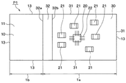
本発明の第1実施形態にかかるモールドパッケージP1について、図1、図2を参照して述べる。このモールドパッケージP1は、たとえば自動車などの車両に搭載され、車両用の各種電子装置を駆動するための装置として適用されるものである。なお、図2に示される平面図中では、モールド樹脂30を透過してモールド樹脂30の内部に位置する構成要素を実線にて示している。
(First embodiment)
The mold package P1 according to the first embodiment of the present invention will be described with reference to FIGS. The mold package P1 is mounted on a vehicle such as an automobile and is applied as a device for driving various electronic devices for the vehicle. In the plan view shown in FIG. 2, components that pass through the
本実施形態のモールドパッケージP1は、大きくは、一面11と他面12とが表裏の板面の関係にある基板10と、基板10の一面11に搭載された電子部品20、21と、基板10の一面11に設けられ、電子部品20、21とともに基板10の一面11を封止するモールド樹脂30と、を備えている。
The mold package P1 of the present embodiment is broadly divided into a
ここで、基板10における一面11とは反対側の他面12は、モールド樹脂30より露出している。このように、モールドパッケージP1は、ハーフモールドタイプのものとされている。
Here, the
基板10は、プリント基板等の樹脂よりなるものであり、典型的には、平面矩形の板状をなす。ここでは、図2に示されるように、基板10は、一面11と他面12とが表裏の板面とされ、4個の端面13により外郭が規定された矩形板状をなす。ここで、基板10の一面11には、電子部品20、21を搭載して接続するためのワイヤランド40や部品ランド41が設けられている。
The
電子部品20、21としては、基板10の一面11に搭載可能な表面実装部品、あるいは、スルーホール実装部品などが挙げられる。ここでは、電子部品として、ICチップ20と受動素子21とが示されている。
Examples of the
ICチップ20は、はんだやAgペースト等の図示しないマウント材を介して基板10の一面11に固定され、AuやAl等のボンディングワイヤ22によってワイヤランド40に接続されている。また、受動素子21は、コンデンサや抵抗等であり、これも図示しない上記マウント材によって部品ランド41に接合されている。
The
モールド樹脂30は、通常この種のモールドパッケージに用いられるモールド材料よりなり、必要に応じて、当該樹脂中にアルミナやシリカ等のフィラーが含有されたものである。このモールド樹脂30は、トランスファーモールド法やコンプレッションモールド法等の金型により形成される。
The
モールド樹脂30は、基板10の一面11の一部である封止部1aを封止しつつ当該一面11の残部を露出部1bとして露出させるように、基板10の一面11に配置されている。ここで、基板10の一面のうち封止部1aは、上記電子部品20、21が搭載されている部位であり、露出部1bは、露出部1b上の図示しない配線等により外部と接続したりする部位である。
The
このようなモールドパッケージP1は、MAP成形により製造される。すなわち、モールドパッケージP1は、多連状態の基板10を、金型を用いてモールド樹脂30で一括して封止した後、モールド樹脂30とともに基板10を切断して個片化することにより、形成される。
Such a mold package P1 is manufactured by MAP molding. That is, the mold package P1 is formed by sealing the
ここで、基板10の一面11の上方から視たときのモールド樹脂30の平面形状は、図2に示されるように、MAP成形による典型的な矩形をなしている。つまり、モールド樹脂30は、4個の側面31、32にて外郭を規定された矩形板状とされている。
Here, the planar shape of the
また、モールド樹脂30のうち基板10の一面11とは反対側の板面である上面33は、全体が平坦な平坦面とされている。これは、MAP成形によれば、金型でモールド樹脂30が成形されるのでポッティング等により成形されたモールド樹脂とは異なり、モールド樹脂30における上面33は、金型の内面に対応した平坦面となるためである。なお、ポッティング成形の場合には、典型的には、モールド樹脂の上面は凸曲面となる。
Moreover, the
そして、この平面矩形をなすモールド樹脂30における4個の側面31、32のうち3個の側面は、基板10の端面13と同一平面に位置する端部側面31とされている。一方、モールド樹脂30における4個の側面31、32のうち残り1個の側面は、基板10の一面11における封止部1aと露出部1bとの境界部に位置して基板10の一面11から当該一面11上に延びる境界部側面32とされている。
Of the four
ここで、モールド樹脂30の端部側面31は、上記MAP成形におけるモールド樹脂30および基板10の切断により形成される切断面として構成されている。一方、モールド樹脂30の境界部側面32は、金型の内面により成形された面として構成されている。
Here, the
そして、この境界部側面32は、基板10の一面11とのなす角度すなわち基板10の一面11に対する傾斜角θが鋭角となるように、基板10の一面11に対して傾斜した傾斜面とされている。
The
ここでは、境界部側面32は、基板10の一面11に接する下端部32aからモールド樹脂30の上面33との境界である上端部32bまで均一な傾斜角θを有するものとされている。つまり、境界部側面32の全体が、傾斜角θを有する傾斜面とされている。
Here, the boundary
ここで、本実施形態では、この傾斜角θを30°以上75°以下としている。これは、車両での使用時における冷熱サイクルにより発生する熱変形によって、基板10における封止部1aと露出部1bとの境界部にて発生する基板10やモールド樹脂30へのダメージを抑制するためである。この傾斜角θの範囲の根拠については、後述する。
Here, in the present embodiment, the inclination angle θ is set to 30 ° to 75 °. This is to suppress damage to the
ここで、モールドパッケージP1における基板10およびモールド樹脂30の材質、寸法について、具体例を述べておく。なお、この具体例は、この種の典型的なモールドパッケージにおける材質および寸法である。
Here, specific examples of the materials and dimensions of the
まず、基板10およびモールド樹脂30は、ポリアクリル系樹脂、ポリイミド系樹脂、エポキシ系樹脂などの典型的な樹脂材料から構成される。また、基板10の厚さ(つまり板厚)およびモールド樹脂30の厚さ(つまり板厚)については、特に規定しないが、好ましくは、モールド樹脂30の方が基板10よりも厚いものとする。
First, the
たとえば、基板10の厚さを1としたとき、モールド樹脂30の厚さは2.5〜5とすることが望ましい。このような厚さの関係を満足した上で、たとえば、基板10の厚さは0.6〜1.6mm程度であり、モールド樹脂30の厚さは2.0〜6.0mm程度である。
For example, when the thickness of the
また、基板10の物性については、好ましくは線膨張係数が8〜20ppm、ヤング率が10〜40GPaである。モールド樹脂30の物性については、好ましくは線膨張係数が9〜20ppm、ヤング率が10〜30GPaである。
The physical properties of the
ここで、図3を参照して、上記傾斜角θを30°以上75°以下とした根拠について述べる。この図3は、モールドパッケージP1について、上記具体例に示したような典型的な材質および寸法を適用し、これについて実験および検討を行うことによって求めたグラフである。 Here, with reference to FIG. 3, the grounds for setting the inclination angle θ to 30 ° or more and 75 ° or less will be described. FIG. 3 is a graph obtained by applying typical materials and dimensions as shown in the above specific example to the mold package P1 and conducting experiments and examinations thereof.
図3では、傾斜角θを変えた時の基板10の境界部に発生する破断応力と、境界部側面32におけるモールド樹脂30の部分の破断強度とを、確認した結果が示されている。ここでは、横軸に傾斜角θ、左の縦軸に黒丸プロットとしての上記基板10の破断応力、右の縦軸に白四角プロットとしての上記モールド樹脂30の破断強度を示している。
FIG. 3 shows the results of confirming the breaking stress generated at the boundary portion of the
図3において、上記基板10の破断応力は、上記熱変形によって基板10の境界部にて基板10にクラックが発生する応力である。この破断応力は、シミュレーションにより求め、標準偏差−4σの確率で熱変形により基板10にクラックが発生する値を1と規格化し、図3では相対値を示している。
In FIG. 3, the breaking stress of the
また、図3において、上記モールド樹脂30の破断強度は、傾斜面である境界部側面32におけるモールド樹脂30の部分が、上記熱変形によって割れを発生する強度である。なお、境界部側面32におけるモールド樹脂30の部分とは、図1、図2に示されるように、モールド樹脂30のうち境界部側面32の直下に位置する部分である。
In FIG. 3, the breaking strength of the
当該部分は、境界部側面32が傾斜面であるがゆえに、モールド樹脂30のうち上面33の直下に位置する部分に比べて、薄いものとされている。ここでは、モールド樹脂30の破断強度は、実験等により求め、標準偏差+4σの確率で熱変形によりモールド樹脂30の当該部分に割れが発生する値を1と規格化し、図3では相対値を示している。
Since the
図3に示されるように、基板10の破断応力およびモールド樹脂30の破断強度は、モールド樹脂30の境界部側面32の傾斜角θが大きくなるにつれて大きくなっていき、当該傾斜角θが小さくなるにつれて小さくなっていく。
As shown in FIG. 3, the breaking stress of the
つまり、傾斜角θが大きくなると、境界部側面32におけるモールド樹脂30の部分では、当該モールド樹脂30が厚くなることから破断強度は大きくなるが、逆に基板10の破断応力も大きくなるので、基板10のクラックが発生しやすくなる。一方、傾斜角θが小さくなると、基板10の破断応力は小さくなるが、逆に、境界部側面32におけるモールド樹脂30の部分では、当該モールド樹脂30が薄くなることから、割れが生じやすくなる。
That is, when the inclination angle θ is increased, the portion of the
そこで、本発明者は、基板10の破断応力およびモールド樹脂30の破断強度について、標準偏差4σよりも厳しい基準である標準偏差6σとなる値を基準とすることにした。図3には、上記破断応力の標準偏差−6σとなる値0.8をA1で示し、上記破断強度の標準偏差6σとなる値1.2をB1で示している。
Therefore, the inventor decided to use a value that gives a standard deviation 6σ, which is a stricter standard than the standard deviation 4σ, for the breaking stress of the
まず、基板10の破断応力については、傾斜角θが75°であるとき、0.8すなわち標準偏差−6σの値A1となる。これにより、傾斜角θは75°以下とした。このように傾斜角θを75°以下とすれば、標準偏差6σの確率で、上記した熱変形による基板へのクラック発生を防止できる。
First, the breaking stress of the
一方、モールド樹脂30の破断強度については、傾斜角θが30°であるとき、1.2すなわち標準偏差+6σの値B1となる。これにより、傾斜角θは30°以上とした。このように傾斜角θを30°以上とすれば、標準偏差6σの確率で、上記した熱変形によるモールド樹脂の割れ発生を防止できる。
On the other hand, the breaking strength of the
以上のように、本実施形態によれば、傾斜角θを30°以上75°以下とすれば、基板10における封止部1aと露出部1bとの境界部における基板10のクラック発生およびモールド樹脂30の割れ発生を、製品の品質保証上、実質問題無いレベルにて抑制することができる。そのため、当該境界部にて発生する基板10やモールド樹脂30へのダメージを適切に抑制することができる。
As described above, according to the present embodiment, when the inclination angle θ is 30 ° or more and 75 ° or less, the occurrence of cracks in the
(第2実施形態)
本発明の第2実施形態にかかるモールドパッケージP2について、図4を参照して、上記第1実施形態との相違点を中心に述べる。
(Second Embodiment)
The mold package P2 according to the second embodiment of the present invention will be described with reference to FIG. 4 focusing on differences from the first embodiment.
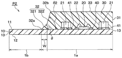
上記第1実施形態では、モールド樹脂30の境界部側面32の全体が、傾斜角θを有する傾斜面とされていた。それに対して、本実施形態では、境界部側面32は、基板10の一面11に接する下端部32a側の部位321と、上端部32b側の部位322との境界が凹むように屈曲した2段の傾斜構成とされている。
In the said 1st Embodiment, the whole boundary
具体的に、本実施形態では、境界部側面32のうち下端部32a側の部位321が、上記傾斜角θを有する傾斜面であり、上端部32b側の部位322は、基板10の一面11に対する傾斜角θ2が上記傾斜角θよりも大きく且つ90°以下である面とされている。つまり、下端部32a側の部位321の傾斜角θは、30°≦θ≦75°であり、上端部32b側の部位322の傾斜角θ2は、θ<θ2≦90°である。
Specifically, in the present embodiment, the
このような2段の傾斜構成を採用することにより、モールド樹脂30における境界部側面32の部分において、モールド樹脂30の薄い部分を少ないものにできる。具体的には、傾斜角θを小さくしても、モールド樹脂30のうち下端部32a側の部位の直下に位置する部分は薄くなるが、それに比して、上端部32b側の部位322の直下に位置する部分では、厚さを確保できる。
By adopting such a two-step inclined configuration, the thin portion of the
そのため、本実施形態では、封止部1aと露出部1bとの境界部におけるモールド樹脂30の割れを抑制するという点で、好ましい。この点を考慮すれば、図4に示されるように、モールド樹脂30のうち下端部32a側の部位の直下に位置する部分の幅Wは、傾斜角θが30°の場合、0.5mm以下であることが望ましい。
Therefore, in this embodiment, it is preferable at the point of suppressing the crack of the
また、本実施形態においても、境界部側面32における下端部32a側の部位321の傾斜面構成が、上記第1実施形態と同様のものであることから、上記同様に、上記境界部における基板10のクラック発生およびモールド樹脂30の割れ発生を抑制することができる。
Also in this embodiment, since the inclined surface configuration of the
つまり、モールド樹脂30の境界部側面32のうち少なくとも下端部32a側の部位321が、30°〜75°の傾斜角θを有する傾斜面とされた構成であれば、上記境界部にて発生する基板10やモールド樹脂30へのダメージを適切に抑制することができる。
That is, if at least the
(第3実施形態)
本発明の第3実施形態にかかるモールドパッケージP3について、図5を参照して述べる。本実施形態では、基板10の一面11の露出部1b上には、モールド樹脂30で封止されない他の部品として受動素子23が搭載されている。この受動素子23は、上記第1実施形態の受動素子21に採用可能なものから選択されたものとされるが、当該他の部品としては、受動素子以外の表面実装部品やスルーホール実装部品であってもよい。
(Third embodiment)
A mold package P3 according to a third embodiment of the present invention will be described with reference to FIG. In the present embodiment, the
(他の実施形態)
なお、上記各実施形態では、モールド樹脂30の4個の側面のうち3辺が端部側面31、残りの1辺が境界部側面32であったが、これに限定するものではなく、図6に示されるように、当該4辺の側面のうち2辺が端部側面31で、残りの2辺が境界部側面32でもよい。
(Other embodiments)
In each of the above embodiments, three of the four side surfaces of the
さらには、図示しないけれども、当該4辺の側面のうち1辺が端部側面31で、残りの3辺が境界部側面32であってもよい。つまり、モールド樹脂30としては、4個の側面において端部側面31、境界部側面32が、それぞれ少なくとも1つ、あればよい。
Further, although not shown, one of the four side surfaces may be the
また、上記第2実施形態において、境界部側面32における上端部32b側の部位322を、さらに多段階に傾斜させた構成としてもよい。ただし、この場合でも上端部32b側の部位322における複数の傾斜面の傾斜角が、下端部32a側の部位321の傾斜角θよりも大きく且つ90°以下であることが必要である。
Moreover, in the said 2nd Embodiment, it is good also as a structure which inclined the
また、本発明は上記した実施形態に限定されるものではなく、特許請求の範囲に記載した範囲内において適宜変更が可能である。また、上記各実施形態は、互いに無関係なものではなく、組み合わせが明らかに不可な場合を除き、適宜組み合わせが可能であり、また、上記各実施形態は、上記の図示例に限定されるものではない。 Further, the present invention is not limited to the above-described embodiment, and can be appropriately changed within the scope described in the claims. The above embodiments are not irrelevant to each other, and can be combined as appropriate unless the combination is clearly impossible, and the above embodiments are not limited to the illustrated examples. Absent.
1a 基板の一面の封止部
1b 基板の一面の露出部
10 基板
11 基板の一面
12 基板の他面
13 基板の端面
20 電子部品としてのICチップ
21 電子部品としての受動素子
30 モールド樹脂
31 モールド樹脂の端部側面
32 モールド樹脂の境界部側面
θ 境界部側面の傾斜角
DESCRIPTION OF
Claims (3)
前記基板の一面に搭載された電子部品(20、21)と、
前記基板の一面に設けられ、前記電子部品とともに前記基板の一面を封止するモールド樹脂(30)と、を備え、
前記基板の他面は、前記モールド樹脂より露出しているハーフモールドタイプのモールドパッケージであって、
前記モールド樹脂は、前記基板の一面の一部である封止部(1a)を封止しつつ当該一面の残部を露出部(1b)として露出させるように、前記基板の一面に配置されたものであり、
前記モールド樹脂における側面(31、32)のうち少なくとも1つの側面は、前記基板の端面(13)と同一平面に位置する端部側面(31)とされており、
前記モールド樹脂における側面のうち少なくとも1つの側面は、前記基板の一面における前記封止部と前記露出部との境界部に位置して前記基板の一面から当該一面上に延びる境界部側面(32)とされており、
前記境界部側面のうち、少なくとも前記基板の一面に接する下端部(32a)側の部位は、前記基板の一面に対する傾斜角(θ)が鋭角となるように、前記基板の一面に対して傾斜した傾斜面とされており、
前記傾斜角は30°以上75°以下であり、
前記境界部側面のうち、前記下端部側の部位(321)が前記傾斜角を有する傾斜面であり、
前記境界部側面のうち、前記下端部側の部位よりも上端部(32b)側の部位(322)は、前記基板の一面に対する傾斜角が前記下端部側の部位よりも大きく且つ90°以下である面とされていることを特徴とするモールドパッケージ。 A substrate (10) made of a resin in which one surface (11) and the other surface (12) are in a relation of front and back plate surfaces;
Electronic components (20, 21) mounted on one surface of the substrate;
A mold resin (30) provided on one surface of the substrate and sealing the one surface of the substrate together with the electronic component;
The other surface of the substrate is a half mold type mold package exposed from the mold resin,
The mold resin is arranged on one surface of the substrate so that the sealing portion (1a) which is a part of one surface of the substrate is sealed and the remaining portion of the one surface is exposed as an exposed portion (1b). It is in,
Wherein at least one side of the put that side of the mold resin (31, 32) is an end side (31) located in the same plane as the end face of the substrate (13),
At least one side of the side that put in the mold resin, the sealing portion and the boundary portion side extending from one surface of the substrate located at the boundary portion between the exposed portion on the one side in one surface of the substrate ( 32)
Of the side surface of the boundary portion, at least a portion on the lower end portion (32a) side in contact with one surface of the substrate is inclined with respect to the one surface of the substrate such that an inclination angle (θ) with respect to the one surface of the substrate is an acute angle. It is an inclined surface,
The inclination angle is not less than 30 ° and not more than 75 ° ,
Of the boundary side surface, the lower end side portion (321) is an inclined surface having the inclination angle,
Of the side surface of the boundary portion, the portion (322) on the upper end portion (32b) side of the portion on the lower end side is larger in inclination angle with respect to one surface of the substrate than the portion on the lower end side and 90 ° or less. A mold package characterized by having a certain surface .
Priority Applications (4)
| Application Number | Priority Date | Filing Date | Title |
|---|---|---|---|
| JP2014010397A JP6194804B2 (en) | 2014-01-23 | 2014-01-23 | Mold package |
| CN201580005263.4A CN106415825B (en) | 2014-01-23 | 2015-01-09 | Molded packages |
| PCT/JP2015/000074 WO2015111376A1 (en) | 2014-01-23 | 2015-01-09 | Molded package |
| US15/104,255 US9601442B2 (en) | 2014-01-23 | 2015-01-09 | Half-mold type mold package |
Applications Claiming Priority (1)
| Application Number | Priority Date | Filing Date | Title |
|---|---|---|---|
| JP2014010397A JP6194804B2 (en) | 2014-01-23 | 2014-01-23 | Mold package |
Publications (3)
| Publication Number | Publication Date |
|---|---|
| JP2015138907A JP2015138907A (en) | 2015-07-30 |
| JP2015138907A5 JP2015138907A5 (en) | 2016-03-10 |
| JP6194804B2 true JP6194804B2 (en) | 2017-09-13 |
Family
ID=53681191
Family Applications (1)
| Application Number | Title | Priority Date | Filing Date |
|---|---|---|---|
| JP2014010397A Expired - Fee Related JP6194804B2 (en) | 2014-01-23 | 2014-01-23 | Mold package |
Country Status (4)
| Country | Link |
|---|---|
| US (1) | US9601442B2 (en) |
| JP (1) | JP6194804B2 (en) |
| CN (1) | CN106415825B (en) |
| WO (1) | WO2015111376A1 (en) |
Families Citing this family (1)
| Publication number | Priority date | Publication date | Assignee | Title |
|---|---|---|---|---|
| US10796976B2 (en) | 2018-10-31 | 2020-10-06 | Taiwan Semiconductor Manufacturing Company, Ltd. | Semiconductor device and method of forming the same |
Family Cites Families (13)
| Publication number | Priority date | Publication date | Assignee | Title |
|---|---|---|---|---|
| KR100386061B1 (en) | 1995-10-24 | 2003-08-21 | 오끼 덴끼 고오교 가부시끼가이샤 | Semiconductor device and lead frame with improved construction to prevent cracking |
| JPH1020483A (en) | 1996-06-28 | 1998-01-23 | Toppan Printing Co Ltd | Photosensitive resin composition |
| KR100255108B1 (en) * | 1997-06-18 | 2000-05-01 | Samsung Electronics Co Ltd | Chip card |
| JP3332814B2 (en) * | 1997-08-12 | 2002-10-07 | アピックヤマダ株式会社 | Substrate mold and molded substrate |
| JPH11340378A (en) * | 1998-05-22 | 1999-12-10 | Sanken Electric Co Ltd | Manufacture of semiconductor light emitting device |
| JP3619773B2 (en) * | 2000-12-20 | 2005-02-16 | 株式会社ルネサステクノロジ | Manufacturing method of semiconductor device |
| JP2003304004A (en) * | 2002-04-11 | 2003-10-24 | Citizen Electronics Co Ltd | Optical transmission chip and mounting structure thereof |
| FI119400B (en) * | 2003-03-14 | 2008-10-31 | Outotec Oyj | Procedure for regulating a process |
| JP2006269486A (en) * | 2005-03-22 | 2006-10-05 | Renesas Technology Corp | Method for manufacturing semiconductor apparatus |
| CN101944492A (en) * | 2008-10-20 | 2011-01-12 | 联合科技公司 | Shrink package on board |
| JP5051189B2 (en) | 2009-07-10 | 2012-10-17 | アイシン・エィ・ダブリュ株式会社 | Electronic circuit equipment |
| JP5794156B2 (en) | 2012-01-24 | 2015-10-14 | 株式会社デンソー | Mold package manufacturing method |
| JP6115505B2 (en) | 2013-06-21 | 2017-04-19 | 株式会社デンソー | Electronic equipment |
-
2014
- 2014-01-23 JP JP2014010397A patent/JP6194804B2/en not_active Expired - Fee Related
-
2015
- 2015-01-09 US US15/104,255 patent/US9601442B2/en active Active
- 2015-01-09 WO PCT/JP2015/000074 patent/WO2015111376A1/en active Application Filing
- 2015-01-09 CN CN201580005263.4A patent/CN106415825B/en not_active Expired - Fee Related
Also Published As
| Publication number | Publication date |
|---|---|
| WO2015111376A1 (en) | 2015-07-30 |
| JP2015138907A (en) | 2015-07-30 |
| US9601442B2 (en) | 2017-03-21 |
| CN106415825B (en) | 2019-04-19 |
| CN106415825A (en) | 2017-02-15 |
| US20160293555A1 (en) | 2016-10-06 |
Similar Documents
| Publication | Publication Date | Title |
|---|---|---|
| JP6193510B2 (en) | Lead frame, semiconductor device, lead frame manufacturing method, and semiconductor device manufacturing method | |
| US20140048918A1 (en) | Semiconductor device and method of manufacturing the same | |
| JP4705881B2 (en) | Lead frame and semiconductor device using the same | |
| US7952177B2 (en) | Resin-sealed semiconductor device, leadframe with die pads, and manufacturing method for leadframe with die pads | |
| US20140042609A1 (en) | Semiconductor device and method of manufacturing the same | |
| JP2009170476A (en) | Semiconductor device and method of manufacturing the same | |
| JP6677616B2 (en) | Method for manufacturing semiconductor device | |
| JP2010050406A (en) | Semiconductor device, method of manufacturing semiconductor device, and electronic apparatus | |
| JP6048238B2 (en) | Electronic equipment | |
| JP6406121B2 (en) | High frequency high power device | |
| JP6194804B2 (en) | Mold package | |
| JP2010021251A (en) | Semiconductor device and its manufacturing method | |
| US9196590B2 (en) | Perforated electronic package and method of fabrication | |
| JP5949667B2 (en) | Mold package and manufacturing method thereof | |
| JP2016146458A (en) | Semiconductor device | |
| JP2020035820A (en) | Module and manufacturing method thereof | |
| JP6767772B2 (en) | Package for storing electronic components and electronic devices using it | |
| JP5458476B2 (en) | Mold package and manufacturing method thereof | |
| JP2010080567A (en) | Multi-piece substrate, wiring board, and electronic apparatus | |
| JPWO2018123382A1 (en) | Circuit module | |
| WO2011049234A1 (en) | Substrate and method for manufacturing circuit device using same | |
| JP4695672B2 (en) | Semiconductor device | |
| US20220301984A1 (en) | Semiconductor device | |
| JP6163886B2 (en) | Mold package | |
| JP2020202292A (en) | Semiconductor devices and method for manufacturing semiconductor device |
Legal Events
| Date | Code | Title | Description |
|---|---|---|---|
| A521 | Request for written amendment filed |
Free format text: JAPANESE INTERMEDIATE CODE: A523 Effective date: 20160120 |
|
| A621 | Written request for application examination |
Free format text: JAPANESE INTERMEDIATE CODE: A621 Effective date: 20160810 |
|
| TRDD | Decision of grant or rejection written | ||
| A01 | Written decision to grant a patent or to grant a registration (utility model) |
Free format text: JAPANESE INTERMEDIATE CODE: A01 Effective date: 20170718 |
|
| A61 | First payment of annual fees (during grant procedure) |
Free format text: JAPANESE INTERMEDIATE CODE: A61 Effective date: 20170731 |
|
| R151 | Written notification of patent or utility model registration |
Ref document number: 6194804 Country of ref document: JP Free format text: JAPANESE INTERMEDIATE CODE: R151 |
|
| R250 | Receipt of annual fees |
Free format text: JAPANESE INTERMEDIATE CODE: R250 |
|
| LAPS | Cancellation because of no payment of annual fees |