EP2706444A2 - Berührungsanzeige - Google Patents
Berührungsanzeige Download PDFInfo
- Publication number
- EP2706444A2 EP2706444A2 EP13182676.0A EP13182676A EP2706444A2 EP 2706444 A2 EP2706444 A2 EP 2706444A2 EP 13182676 A EP13182676 A EP 13182676A EP 2706444 A2 EP2706444 A2 EP 2706444A2
- Authority
- EP
- European Patent Office
- Prior art keywords
- liquid crystal
- crystal display
- quarter
- wave plate
- sensitive panel
- Prior art date
- Legal status (The legal status is an assumption and is not a legal conclusion. Google has not performed a legal analysis and makes no representation as to the accuracy of the status listed.)
- Withdrawn
Links
Images


Classifications
-
- G—PHYSICS
- G06—COMPUTING OR CALCULATING; COUNTING
- G06F—ELECTRIC DIGITAL DATA PROCESSING
- G06F3/00—Input arrangements for transferring data to be processed into a form capable of being handled by the computer; Output arrangements for transferring data from processing unit to output unit, e.g. interface arrangements
- G06F3/01—Input arrangements or combined input and output arrangements for interaction between user and computer
- G06F3/03—Arrangements for converting the position or the displacement of a member into a coded form
- G06F3/041—Digitisers, e.g. for touch screens or touch pads, characterised by the transducing means
- G06F3/0412—Digitisers structurally integrated in a display
-
- G—PHYSICS
- G02—OPTICS
- G02F—OPTICAL DEVICES OR ARRANGEMENTS FOR THE CONTROL OF LIGHT BY MODIFICATION OF THE OPTICAL PROPERTIES OF THE MEDIA OF THE ELEMENTS INVOLVED THEREIN; NON-LINEAR OPTICS; FREQUENCY-CHANGING OF LIGHT; OPTICAL LOGIC ELEMENTS; OPTICAL ANALOGUE/DIGITAL CONVERTERS
- G02F1/00—Devices or arrangements for the control of the intensity, colour, phase, polarisation or direction of light arriving from an independent light source, e.g. switching, gating or modulating; Non-linear optics
- G02F1/01—Devices or arrangements for the control of the intensity, colour, phase, polarisation or direction of light arriving from an independent light source, e.g. switching, gating or modulating; Non-linear optics for the control of the intensity, phase, polarisation or colour
- G02F1/13—Devices or arrangements for the control of the intensity, colour, phase, polarisation or direction of light arriving from an independent light source, e.g. switching, gating or modulating; Non-linear optics for the control of the intensity, phase, polarisation or colour based on liquid crystals, e.g. single liquid crystal display cells
- G02F1/133—Constructional arrangements; Operation of liquid crystal cells; Circuit arrangements
- G02F1/1333—Constructional arrangements; Manufacturing methods
- G02F1/13338—Input devices, e.g. touch panels
-
- G—PHYSICS
- G06—COMPUTING OR CALCULATING; COUNTING
- G06F—ELECTRIC DIGITAL DATA PROCESSING
- G06F2203/00—Indexing scheme relating to G06F3/00 - G06F3/048
- G06F2203/041—Indexing scheme relating to G06F3/041 - G06F3/045
- G06F2203/04103—Manufacturing, i.e. details related to manufacturing processes specially suited for touch sensitive devices
-
- G—PHYSICS
- G06—COMPUTING OR CALCULATING; COUNTING
- G06F—ELECTRIC DIGITAL DATA PROCESSING
- G06F3/00—Input arrangements for transferring data to be processed into a form capable of being handled by the computer; Output arrangements for transferring data from processing unit to output unit, e.g. interface arrangements
- G06F3/01—Input arrangements or combined input and output arrangements for interaction between user and computer
- G06F3/03—Arrangements for converting the position or the displacement of a member into a coded form
- G06F3/041—Digitisers, e.g. for touch screens or touch pads, characterised by the transducing means
- G06F3/044—Digitisers, e.g. for touch screens or touch pads, characterised by the transducing means by capacitive means
Definitions
- the present invention relates to a touch display.
- a vehicle such as an automobile has an instrument panel installed at the front of the interior of the vehicle.
- One or more instrumental devices displaying information needed for a driver are installed at the driver's side or at the midpoint of the driver's side and the passenger's side of the instrument panel.
- one or more control panels to control an air-conditioner or an audio device are installed at the midpoint of the driver's side and the passenger's side of the instrument panel. Therefore, instrumental devices and control panels which have a display device including a liquid crystal display have been developed.
- touch display devices having a liquid crystal display and enabling an input operation to be performed by touching a screen with a fingertip.
- touch displays are becoming widely used and are expected to be installed in many vehicles in the future.
- Some of these touch displays use a resistive touch-sensitive panel or a capacitive touch-sensitive panel.
- the resistive touch-sensitive panel has a configuration in which two transparent conductive films are arranged one above the other at an interval by spacers, and senses a touch operation from upper and lower transparent films partly in contact with each other.
- the touch display using a resistive touch-sensitive panel is the most widespread touch display in use.
- a capacitive touch-sensitive panel senses the variation of capacitance when the fingertip contacts or comes in close contact to a screen.
- Such a capacitive touch-sensitive panel has a higher sensitivity than a resistive touch-sensitive panel since it does not require a touch-pressure-sensitive operation.
- Such capacitive touch-sensitive panels are expected to be widespread in the future.
- FIG.9 illustrates a general capacitance touch display 1 wherein a capacitive touch-sensitive panel 4 is attached to a surface (outer surface) of a liquid crystal display 2, and a decorated sheet 3 is attached to the capacitive touch-sensitive panel 4
- the decorated sheet 3 is directly attached to a surface (outer surface) of the capacitive touch-sensitive panel 4, and they are arranged at a position in a front side of the liquid crystal display 2 through a thin layer of air 5. Moreover, a polarizer 6 which forms a part of the liquid crystal display 2 is integrally arranged on the surface of the liquid crystal display 2 in advance.
- outside light L is reflected at respective boundary planes between outside air and the decorated sheet 3, the decorated sheet 3 and the capacitive touch-sensitive panel 4, and the capacitive touch-sensitive panel 4 and the layer of air 5 (reflected light La, Lb and Lc).
- a level of reflectance depends on a level of refractive index at the boundary planes. Therefore, a maximum reflection occurs at a boundary with air having a maximum refractive index.
- the reflectance of the touch display 1 having the foregoing configuration is 8% ⁇ 9%, thus providing high reflection.
- the touch display When the touch display is installed in a vehicle such as an automobile, the touch display is often exposed to direct sunlight. Moreover, it is difficult to adjust the touch display to an easily viewable angle with less reflection.
- Patent Document 1 Japanese Patent Application Publication No. 2000-321558
- the touch display disclosed in Patent Document 1 decreases reflectance by providing a polarizer, a quarter-wave plate, a resistive touch-sensitive panel, a second quarter-wave plate, and a plurality of decorated sheets having optical isotropy, arranged to the liquid crystal display in order from the outside toward the surface of the liquid crystal display.
- the configuration of a touch display disclosed in Patent Document 1 uses a resistive touch-sensitive panel.
- the resistive touch-sensitive panel has a configuration in which transparent conductive films are arranged one above the other at an interval by spacers, and a touch operation is sensed by a partial contact of upper and lower transparent films.
- the touch operation cannot be sensed accurately due to a reduction in sensitivity of the resistive touch-sensitive panel if there are a number of adhered or coating layers on the surface (outer surface) of the resistive touch-sensitive panel.
- a decorated sheet formed of a thick film must be attached to a reverse side of the resistive touch-sensitive panel instead of an obverse side thereof.
- the present invention aims to provide a touch display having a high antireflection structure while keeping costs low.
- a touch display capable of an input operation in reaction to a displayed image, comprising a liquid crystal display displaying images, and a capacitive touch-sensitive panel superposed on a surface of the liquid crystal display, wherein a second quarter-wave plate converting light passing through into circularly-polarized light by a shifting phase, a capacitive touch-sensitive panel, a first quarter-wave plate having the same orientation as the second quarter-wave plate, a polarizer converting light passing through into polarized light, a decorated sheet protecting an upper surface of the capacitive touch-sensitive panel, and an antireflection layer preventing surface-reflection of outside light are provided on the liquid crystal display in order from the surface of the liquid crystal display toward an outer surface of the liquid crystal display.
- the following function effects can be obtained by the configuration described above. That is to say, at first, most of the reflection of the outside light is minimized by the antireflection layer arranged at an outermost part. At that time, the reflection of the outside light is highest at the boundary with air. Therefore, the highest effect of antireflection is obtained by arranging the antireflection layer at the outermost part.
- the reflected light from an upper surface of the capacitive touch-sensitive panel and the reflected light from the rear surface of the capacitive touch-sensitive panel will be cut by the polarizer. As a result, the reflectance can be minimized to approximately 1% or less.
- the outside light passing through the decorated sheet is unpolarized light. And the outside light is converted into linearly-polarized light by passing through the polarizer. Further, the outside light, which is now linearly-polarized light, is converted into circularly-polarized light by passing through the first quarter-wave plate.
- part of the outside light which is now circularly-polarized light, is reflected at the surface of the capacitive touch-sensitive panel and converted into counter-rotating circularly-polarized light by phase-reversal.
- the reflected light which is now counter-rotating circularly-polarized light, is converted into the linearly-polarized light once again by passing through the first quarter-wave plate.
- the reflected light which is linearly-polarized light, is perpendicular to the direction of polarization of the polarizer because of the reversed phase thereof and is cut by the polarizer.
- the remaining outside light passing through the first quarter-wave plate and which has become circularly-polarized light is reflected at the rear surface of the second quarter-wave plate and converted into counter-rotating circularly-polarized light by phase-reversal.
- the reflected light, which is now counter-rotating circularly-polarized light is converted into linearly-polarized light once again by passing through the capacitive touch-sensitive panel and the first quarter-wave plate.
- the reflected light which is linearly-polarized light, is perpendicular to the direction of polarization of the polarizer because of the reversed phase thereof and is cut by the polarizer.
- another polarizer is integrally attached to the surface of the liquid crystal display as a part of a configuration of the liquid crystal display in advance.
- An image from the liquid crystal display is converted into linearly-polarized light by the polarizer.
- the image, which is formed by linearly-polarized light is converted into circularly-polarized light by passing through the second quarter-wave plate, and further converted into linearly-polarized light by passing through the capacitive touch-sensitive panel and the first quarter-wave plate.
- This linearly-polarized light can easily pass through the polarizer by aligning its polarizing direction with the polarizing axis of the polarizer. Therefore, the image from the liquid crystal display is visible externally through the decorated sheet and the antireflection layer.
- the decorated sheet can be arranged on the outer side of the capacitive touch-sensitive panel without a decrease in sensing performance by virtue of the fact that the capacitive touch-sensitive panel does not sense pressure with a touch operation. Then, arranging the decorated sheet to the outer side of the capacitive touch-sensitive panel (and the polarizer) allows the use of an inexpensive decorated sheet having optical anisotropy, and decreases the cost. Moreover, a decorated sheet printed in different designs can be directly visible, since the decorated sheet lies close to the surface of the layers. Therefore, a broader choice of design is available and the decorative effect can be improved.
- a vehicle such as an automobile has an instrument panel installed at the front of the interior of a vehicle.
- One or more instrumental devices displaying information needed for a driver are installed at the driver's side or at the midpoint of the driver's side and the passenger's side of the instrument panel.
- one or more control panels to control an air-conditioner or an audio device are installed at the midpoint of the driver's side and the passenger's side of the instrument panel.
- a display device including a liquid crystal display is installed in at least one of the controller of the instrumental device and the control panels.
- a so-called “touch display” is used as at least one display device including the liquid crystal display.
- touch display means a liquid crystal display which can be operated by touching images displayed on the surface of a liquid crystal display with a fingertip.
- the touch display has the liquid crystal display displaying the images and a capacitive touch-sensitive panel superposed on the surface of the liquid crystal display.
- touch-sensitive panels are either the resistive touch-sensitive panel or the capacitive touch-sensitive panel.
- the touch display using the capacitive touch-sensitive panel which is more sensitive than the touch display using the resistive touch-sensitive panel is used.
- the capacitive touch-sensitive panel senses a change in capacitance that occurs when a fingertip is in touch or close to the surface.
- a capacitive touch-sensitive panel has an advantage in that there is no need to sense pressure by fingertip touching.
- the display device having the liquid crystal display is set in a storage recess for display device made at a housing not shown in the figure, and the housing is fixed to a vehicle body.
- a concave portion for a sheet formed to fit the decorated sheet flush with the surface of the housing.
- the concave portion for sheet is assumed to be slightly larger than the storage recess for display device.
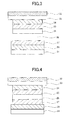
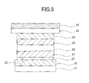
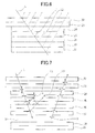
- FIGs. 1 to 7 illustrate the embodiment and its variations.
- the touch display has the following configurations to have a low reflectance of the outside light so as to be suitably built into a vehicle.
- the second quarter-wave plate 27 converting light passing through into circularly-polarized light by a shifting phase
- the decorated sheet 23 protecting the upper surface of the capacitive touch-sensitive panel 26, and the antireflection layer 22 preventing the surface-reflection of an outside light L are arranged on the liquid crystal display 21 in order from the surface of the liquid crystal display toward the outer surface of the liquid crystal display.
- the liquid crystal display 21 is assumed to be made of a liquid crystal cell and a backlight covered with a metal casing.
- a polarizer 28 functioning as a part of the liquid crystal display 21 is provided on the liquid crystal cell.
- the polarizer 28 configures a part of a liquid crystal-shutter to control the image display.
- the polarizer 28 can be antireflection-finished as illustrated in FIG.1 (polarizer with antireflection layer 28a), or pearskin-finished as a variation illustrated in FIG.2 (pearskin-finished polarizer 28b).
- the antireflection layer 22 is assumed to be a resin film which is antireflection-finished and so on.
- an antireflection film such as an AG (Anti-Glare) film or an AR (Anti-Reflection) film is used.
- the AG film is a film with a surface asperity formed by adding particles within it, and prevents the reflection by using a scattering caused by the surface asperity and an inner scattering caused by differences of refraction index between the film and the particles.
- the AR film decreases the reflection by making both reflections from a surface and a rear surface of the film opposite in phase, and cancelling each other.
- the AR film has a metal-oxide layer on its surface.
- the decorated sheet 23 configures a surface design of the display device.
- the decorated sheet 23 has a function to protect the surface.
- various designs are formed on the decorated sheet 23.
- the decorated sheet 23 is formed into the same size as a sheet recess of the casing along with the antireflection layer 22.
- An inexpensive material having optical anisotropy for instance polycarbonate, can be used as the decorated sheet 23. Note that, an expensive material having optical isotropy can be naturally used as the decorated sheet 23, although there is no need for.
- the polarizer 24 is an optical film which allows only light having a particular direction of polarization to pass through.
- the polarizer 24 is arranged in the same orientation of polarization to the polarizer 28 as the liquid crystal display 21.
- the first quarter-wave plate 25 is an optical film which converts light passing through the polarizer 24 into circularly-polarized light by shifting the phase of the direction of polarization.
- the first quarter-wave plate 25 also has another function to convert circularly-polarized light into linearly-polarized light.
- the capacitive touch-sensitive panel 26 is a transparent sensitive panel which senses the change in capacitance when a fingertip touches or comes close to the surface thereof.
- the capacitive touch-sensitive panel 26 has higher sensitivity than the resistive touch-sensitive panel which senses pressure of the touch operation.
- the capacitive touch-sensitive panel 26 is formed mainly of a material having a hard surface such as glass, and the sensing performance is not lost or decreased if the surface is covered by adhered or coating material thicknesses of up to 1.5 mm. Note that, the sum of thicknesses of the antireflection layer 22, the decorated sheet 23, the polarizer 24, and the first quarter-wave plate 25 is less than around 0.8 mm; therefore the thickness becomes approximately half of the 1.5 mm that the capacitive touch-sensitive panel 26 can sense therethrough.
- the second quarter-wave plate 27 is arranged in the same direction as the first quarter-wave plate 25.
- the same optical film as the first quarter-wave plate 25 can be used.
- the polarizer 24, the first quarter-wave plate 25, the capacitive touch-sensitive panel 26 and the second quarter-wave plate 27 can be formed in same size as the screen of the liquid crystal display 21. Therefore, production costs can be reduced.
- the antireflection layer 22, the decorated sheet 23, the polarizer 24, the first quarter-wave plate 25, and the capacitive touch-sensitive panel 26 are integrated into a surface panel.
- the second quarter-wave plate 27 and a second antireflection layer 31 are also integrated into the surface panel.
- the second antireflection layer 31 can be arranged between the second quarter-wave plate 27 and the liquid crystal display 21.
- the second antireflection layer 31 the same material as the (first) antireflection layer 22 can be used.
- the antireflection layer 22, the decorated sheet 23, the polarizer 24, the first quarter-wave plate 25, the capacitive touch-sensitive panel 26, and the second quarter-wave plate 27 are integrated by sticking the layers together with adhesive material.
- the liquid crystal display 21 is separated from the surface panel formed of the capacitive touch-sensitive panel 26 and others by a layer of air 32.
- the term “the capacitive touch-sensitive panel 26 and others” indicates “the surface panel” which is combined layers of the capacitive touch-sensitive panel 26 and adhered or covering layers on the front and the rear side surface thereof.
- the surface panel is manufactured by different processes from the liquid crystal display 21 and attached to the liquid crystal display 21 later.
- the surface panel can be formed without the second antireflection layer 31.
- the second quarter-wave plate 27 is integrated with the liquid crystal display 21 by attaching on the surface of the polarizer 28 of the liquid crystal display 21 instead of a rear surface of the capacitive touch-sensitive panel 26. Therefore, the second quarter-wave plate 27 can produce an effect at the surface of the liquid crystal display 21, and a low reflectance can be obtained as is the case of the surface panel with the second antireflection layer 31.
- the surface panel is formed of the antireflection layer 22, the decorated sheet 23, the polarizer 24, the first quarter-wave plate 25, and the capacitive touch-sensitive panel 26.
- the second quarter-wave plate 27 is attached to the liquid crystal display 21 during the manufacturing processes of the liquid crystal display 21 or later as a part of the liquid crystal display 21.
- At least the antireflection layer 22, the decorated sheet 23, the polarizer 24, the first quarter-wave plate 25, the capacitive touch-sensitive panel 26, and the second quarter-wave plate 27 can be directly and integrally attached to the surface of the liquid crystal display 21.
- the term "directly and integrally attached” means to integrate the liquid crystal display 21 with the surface panel which is generally separated from the liquid crystal display 21.
- the surface panel and the liquid crystal display 21 are integrated by sticking together of their entire surfaces with adhesive material.
- the surface panel is attached to the liquid crystal display 21 as a part thereof, during the manufacturing processes of the liquid crystal display 21 or later.
- the second antireflection layer 31 can be provided between the second quarter-wave plate 27 and the liquid crystal display 21.
- the polarizer 28 functions as a part of the liquid crystal display 21.
- the polarizer 28 can be naturally provided according to the needs of the liquid crystal display 21.
- At least the antireflection layer 22, the decorated sheet 23, the polarizer 24, the first quarter-wave plate 25, the capacitive touch-sensitive panel 26, and the second quarter-wave plate 27 can be integrally attached to the surface of the liquid crystal display 21 through a spacer 33.
- a space thickness of approximately 1 mm is provided between the capacitive touch-sensitive panel 26 and the liquid crystal display 21 to avoid an effect of noise from the liquid crystal display 21. Therefore, the capacitive touch-sensitive panel 26 and others (the surface panel) and the liquid crystal display 21 are adhered to each other by the spacer 33 such as a double-faced adhesive tape with a thickness of approximately 1 mm.
- the spacer 33 is installed at a rim of the surface panel and the liquid crystal display 21. In this case, the surface panel is attached to the liquid crystal display 21 later.
- the capacitive touch-sensitive panel 26 and others (the surface panel) and the liquid crystal display 21 are completely separated, and the layer of air 32 separating these two has the thickness of about 1 mm or more.
- the layer of air 32 is illustrated larger than in reality in FIGs. 1 to 3 .
- the second antireflection layer 31 can be installed between the second quarter-wave plate 27 and the liquid crystal display 21.
- the polarizer 28 functions as a part of the liquid crystal display 21.
- the polarizer 28 can be naturally provided according to the needs of the liquid crystal display 21.
- the reflected light L1 from an upper surface of the capacitive touch-sensitive panel 26 and the reflected light L2 from the rear surface of the capacitive touch-sensitive panel 26 will be cut by the polarizer 24. As a result, the reflectance can be minimized to approximately 1% or less.
- the outside light L passing through the antireflection layer 22 and the decorated sheet 23 is unpolarized light. And the outside light L is converted into linearly-polarized light by passing through the polarizer 24. Further, the outside light L, which is now linearly-polarized light, is converted into circularly-polarized light by passing through the first quarter-wave plate 25.
- a part of the outside light L which is circularly-polarized light, is reflected at the surface of the capacitive touch-sensitive panel 26 and converted into counter-rotating circularly-polarized light by phase-reversal (the reflected light L1).
- the reflected light L1 which is now counter-rotating circularly-polarized light, is converted into linearly-polarized light once again by passing through the first quarter-wave plate 25.
- the reflected light L1 which is the linearly-polarized light, is perpendicular to the direction of polarization of the polarizer 24 because of the reversed phase thereof and cut by the polarizer 24.
- the remaining outside light L passing through the first quarter-wave plate 25 and which has become circularly-polarized light is reflected at the rear surface of the second quarter-wave plate 27 and converted into counter-rotating circularly-polarized light by phase-reversal (the reflected light L2).
- the reflected light L2 which is now counter-rotating circularly-polarized light is converted into linearly-polarized light once again by passing through the capacitive touch-sensitive panel 26 and the first quarter-wave plate 25.
- the reflected light L2 as is the case above, which is the linearly-polarized light, is perpendicular to the direction of polarization of the polarizer 24 because of the reversed phase thereof and is cut by the polarizer 24.
- another polarizer 28 is integrally attached to the surface of the liquid crystal display 21 as a part of a configuration of the liquid crystal display 21 in advance.
- An image G from the liquid crystal display 21 is converted into linearly-polarized light by the polarizer 28.
- the image G which is linearly-polarized light, is converted into circularly-polarized light by passing through the second quarter-wave plate 27, and further converted into linearly-polarized light by passing through the capacitive touch-sensitive panel 26 and the first quarter-wave plate 25.
- This linearly-polarized light can easily pass through the polarizer 24 by aligning its polarizing direction with the polarizing axis of the polarizer 24. Therefore, the image G from the liquid crystal display 21 is visible externally through the decorated sheet 23 and the antireflection layer 22.
- the comparative example shown in FIG.8 has a configuration such that the capacitive touch-sensitive panel 26 and the decorated sheet 23 are attached together, further the antireflection layer 22 is attached to the surface of the decorated sheet 23 and the antireflection layer 31 is attached to the surface of the capacitive touch-sensitive panel 26.
- the highest reflectance obtained is 2%.
- the reflectance of 2% means that the reflection of the outside light such as usual sunlight can be reduced well, but it is difficult to reduce the reflection of the outside light such as late afternoon sunlight which is very strong. Therefore, it is considered unsuitable to apply this configuration to a vehicle.
- the following effect is obtained by arranging to the liquid crystal display 21, in order from the front side, the antireflection layer 22, the decorated sheet 23, the polarizer 24, the first quarter-wave plate 25, the capacitive touch-sensitive panel 26, and the second quarter-wave plate 27.
- the decorated sheet 23 can be arranged on the outer side of the capacitive touch-sensitive panel 26 without a decrease in sensing performance by virtue of the fact that the capacitive touch-sensitive panel 26 does not sense a pressure with touch operation. Then, arranging the decorated sheet 23 to the outer side of the capacitive touch-sensitive panel 26 (and the polarizer 24) allows the use of an inexpensive decorated sheet 23 having optical anisotropy, and decreases the cost. Moreover, the decorated sheet 23 which is printed with different designs can be directly visible, since the decorated sheet 23 lies close to the surface of the surface panel. Therefore, a broader choice of design and an effect of the decoration can be improved.
- the second antireflection layer 31 is arranged between the second quarter-wave plate 27 and the liquid crystal display 21. Therefore, when the second quarter-wave plate 27 and the liquid crystal display 21 are separated by the layer of air 32, the second antireflection layer 31 reduces the reflection from the layer of air 32, and an antireflection effect can be improved.
- the antireflection layer 22, the decorated sheet 23, the polarizer 24, the first quarter-wave plate 25, the capacitive touch-sensitive panel 26, and the second quarter-wave plate 27 are directly and integrally attached to the surface of the liquid crystal display 21. Therefore, due to the fact that the layer of air 32 between the second quarter-wave plate 27 and the liquid crystal display 21 is almost none, the reflection from the layer of air 32 can be eliminated and the reflectance can be minimized. And, since the antireflection layer 22, the decorated sheet 23, the polarizer 24, the first quarter-wave plate 25, the capacitive touch-sensitive panel 26, and the second quarter-wave plate 27 are integrated with the liquid crystal display 21, these layers become easy to handle on the whole.
- the antireflection layer 22, the decorated sheet 23, the polarizer 24, the first quarter-wave plate 25, the capacitive touch-sensitive panel 26, and the second quarter-wave plate 27 are attached to the surface of the liquid crystal display 21 through the spacer 33.
- the second quarter-wave plate 27 and the liquid crystal display 21 are separated by the layer of air 32 having the thickness of the spacer 33. Therefore, the effect of noise from the liquid crystal display 21 can be avoided, in addition to Function effect 3.
Landscapes
- Engineering & Computer Science (AREA)
- Physics & Mathematics (AREA)
- Theoretical Computer Science (AREA)
- General Engineering & Computer Science (AREA)
- General Physics & Mathematics (AREA)
- Nonlinear Science (AREA)
- Human Computer Interaction (AREA)
- Liquid Crystal (AREA)
- Mathematical Physics (AREA)
- Chemical & Material Sciences (AREA)
- Crystallography & Structural Chemistry (AREA)
- Optics & Photonics (AREA)
- Position Input By Displaying (AREA)
- Polarising Elements (AREA)
Applications Claiming Priority (1)
| Application Number | Priority Date | Filing Date | Title |
|---|---|---|---|
| JP2012195913A JP2014052479A (ja) | 2012-09-06 | 2012-09-06 | タッチディスプレイ構造 |
Publications (1)
| Publication Number | Publication Date |
|---|---|
| EP2706444A2 true EP2706444A2 (de) | 2014-03-12 |
Family
ID=49080804
Family Applications (1)
| Application Number | Title | Priority Date | Filing Date |
|---|---|---|---|
| EP13182676.0A Withdrawn EP2706444A2 (de) | 2012-09-06 | 2013-09-02 | Berührungsanzeige |
Country Status (4)
| Country | Link |
|---|---|
| US (1) | US20140063369A1 (de) |
| EP (1) | EP2706444A2 (de) |
| JP (1) | JP2014052479A (de) |
| CN (1) | CN103676269A (de) |
Families Citing this family (18)
| Publication number | Priority date | Publication date | Assignee | Title |
|---|---|---|---|---|
| TWI522857B (zh) * | 2013-10-11 | 2016-02-21 | 群創光電股份有限公司 | 觸控顯示面板、觸控顯示裝置及顯示裝置 |
| CN103682157A (zh) * | 2013-12-10 | 2014-03-26 | 京东方科技集团股份有限公司 | 一种有机电致发光显示器件、其制作方法及显示装置 |
| CN106662777A (zh) * | 2014-09-10 | 2017-05-10 | 松下知识产权经营株式会社 | 液晶显示装置 |
| CN105468185A (zh) * | 2014-09-12 | 2016-04-06 | 南昌欧菲光学技术有限公司 | 一种触控显示屏及移动终端 |
| CN104375703B (zh) * | 2014-11-07 | 2018-03-20 | 苏州欧菲光科技有限公司 | 低反射触控显示屏 |
| CN105700217A (zh) * | 2014-11-26 | 2016-06-22 | 联想(北京)有限公司 | 一种偏光片、液晶显示屏和电子设备 |
| US9927642B2 (en) | 2015-06-18 | 2018-03-27 | Ford Global Technologies, Llc | Vehicle display unit |
| CN106324886A (zh) * | 2015-06-22 | 2017-01-11 | 上海冠显光电科技有限公司 | 一种阳光下可视的显示模组 |
| KR20170000187A (ko) * | 2015-06-23 | 2017-01-02 | 삼성전자주식회사 | 디스플레이 장치 |
| CN106484166A (zh) * | 2015-09-01 | 2017-03-08 | 冠捷投资有限公司 | 触控显示设备及电子装置 |
| JP6921575B2 (ja) * | 2016-03-30 | 2021-08-18 | 株式会社半導体エネルギー研究所 | 表示パネル |
| JP7280009B2 (ja) * | 2016-04-18 | 2023-05-23 | 日東電工株式会社 | 液晶表示装置 |
| CN106199812B (zh) * | 2016-08-30 | 2019-08-06 | 苏州柔彩新材料科技有限公司 | 一种薄化多功能偏光片及其制备方法和应用 |
| KR102446877B1 (ko) * | 2017-05-18 | 2022-09-23 | 삼성전자주식회사 | 디스플레이를 포함하는 전자 장치 |
| CN107910354A (zh) * | 2017-11-24 | 2018-04-13 | 信利光电股份有限公司 | 一种柔性触控显示模组及电子显示设备 |
| KR102608694B1 (ko) * | 2018-04-18 | 2023-12-04 | 삼성전자 주식회사 | 디스플레이 아래에 배치된 센서에 의해 반사된 광을 차단하기 위한 편광 부재 및 위상 지연 부재를 포함하는 전자 장치 |
| CN108920001A (zh) * | 2018-06-29 | 2018-11-30 | 信利光电股份有限公司 | 一种触控显示面板和显示装置 |
| CN110322794B (zh) * | 2019-07-29 | 2025-02-18 | 安徽繁盛显示科技有限公司 | 带圆偏光与触摸屏功能的可折叠超薄玻璃盖板与制作方法 |
Family Cites Families (11)
| Publication number | Priority date | Publication date | Assignee | Title |
|---|---|---|---|---|
| JP2000105669A (ja) * | 1998-01-09 | 2000-04-11 | Nissha Printing Co Ltd | タッチ入力方式の液晶ディスプレイ装置及びその製造方法 |
| JP4177505B2 (ja) * | 1999-02-23 | 2008-11-05 | 日本写真印刷株式会社 | タッチ入力方式液晶ディスプレイ装置 |
| JP3313337B2 (ja) * | 1999-05-13 | 2002-08-12 | 日本写真印刷株式会社 | 低反射タッチパネル |
| JP2001324707A (ja) * | 2000-05-15 | 2001-11-22 | Gunze Ltd | 液晶デイスプレイ用タッチパネル |
| WO2003075207A2 (en) * | 2002-03-01 | 2003-09-12 | Planar Systems, Inc. | Reflection resistant touch screens |
| JP2004117646A (ja) * | 2002-09-25 | 2004-04-15 | Sharp Corp | タッチセンサ付き液晶表示装置およびその製造方法 |
| CN101539676B (zh) * | 2008-03-19 | 2011-04-20 | 胜华科技股份有限公司 | 触控式显示装置、触控式液晶显示装置及其制造方法 |
| TW201145112A (en) * | 2010-02-24 | 2011-12-16 | Alps Electric Co Ltd | Operating device |
| KR101122835B1 (ko) * | 2010-04-23 | 2012-03-21 | 삼성모바일디스플레이주식회사 | 액정표시장치 |
| US8537311B2 (en) * | 2010-11-03 | 2013-09-17 | Blackberry Limited | Display devices containing a circular polarizing system and methods related thereto |
| TWI489182B (zh) * | 2010-12-10 | 2015-06-21 | 友達光電股份有限公司 | 顯示裝置 |
-
2012
- 2012-09-06 JP JP2012195913A patent/JP2014052479A/ja active Pending
-
2013
- 2013-08-28 US US14/012,137 patent/US20140063369A1/en not_active Abandoned
- 2013-09-02 EP EP13182676.0A patent/EP2706444A2/de not_active Withdrawn
- 2013-09-06 CN CN201310404256.4A patent/CN103676269A/zh active Pending
Also Published As
| Publication number | Publication date |
|---|---|
| CN103676269A (zh) | 2014-03-26 |
| US20140063369A1 (en) | 2014-03-06 |
| JP2014052479A (ja) | 2014-03-20 |
Similar Documents
| Publication | Publication Date | Title |
|---|---|---|
| EP2706444A2 (de) | Berührungsanzeige | |
| US8228306B2 (en) | Integration design for capacitive touch panels and liquid crystal displays | |
| EP1100043B1 (de) | Berührungsempfindliche Tafel mit hoher Durchführbarkeit in Umgebungen von niedriger Temperatur | |
| JP5906572B2 (ja) | 表示用前面板の製造方法、および表示装置の製造方法 | |
| US6395863B2 (en) | Touch screen with polarizer and method of making same | |
| US7589798B2 (en) | Touch panel having upper electrode plate including electrode, polarizing plate, quarter wave plate and heat-resistant transparent resin plate | |
| US6707450B2 (en) | Touch panel with polarizer, flat panel display with the touch panel and manufacturing method thereof | |
| US20060017706A1 (en) | Display for stylus input displays | |
| US8243426B2 (en) | Reducing optical effects in a display | |
| KR20150012389A (ko) | 플렉서블 터치 스크린 패널 및 이를 구비한 플렉서블 표시장치 | |
| US9535548B2 (en) | Display device | |
| US20110169767A1 (en) | Polarizer capacitive touch screen | |
| JP2008204320A (ja) | タッチパネル | |
| US20100117988A1 (en) | Optical element and touch sensor | |
| WO2018168387A1 (ja) | タッチパネルおよびそれを備えた意匠構造 | |
| US20220091319A1 (en) | Display device | |
| US20170160846A1 (en) | Touch apparatus | |
| CN102782621B (zh) | 触摸屏模块结构 | |
| US20100259490A1 (en) | Touch Control Electrophoretic Display Module, and Manufacturing Method and Touch Sensing Method for the same | |
| US20110012839A1 (en) | Stacking assembly of a touch panel | |
| US20130002610A1 (en) | Touch sensitive display device | |
| KR100720446B1 (ko) | 편광판 일체형 터치 패널 | |
| US20150220190A1 (en) | Display apparatus | |
| JP6380276B2 (ja) | 表示装置 | |
| US8305353B2 (en) | Glare-resistant touch panel |
Legal Events
| Date | Code | Title | Description |
|---|---|---|---|
| PUAI | Public reference made under article 153(3) epc to a published international application that has entered the european phase |
Free format text: ORIGINAL CODE: 0009012 |
|
| 17P | Request for examination filed |
Effective date: 20130902 |
|
| AK | Designated contracting states |
Kind code of ref document: A2 Designated state(s): AL AT BE BG CH CY CZ DE DK EE ES FI FR GB GR HR HU IE IS IT LI LT LU LV MC MK MT NL NO PL PT RO RS SE SI SK SM TR |
|
| AX | Request for extension of the european patent |
Extension state: BA ME |
|
| STAA | Information on the status of an ep patent application or granted ep patent |
Free format text: STATUS: THE APPLICATION HAS BEEN WITHDRAWN |
|
| 18W | Application withdrawn |
Effective date: 20160209 |