EP2697867B1 - Steckverbinder - Google Patents
Steckverbinder Download PDFInfo
- Publication number
- EP2697867B1 EP2697867B1 EP12701983.4A EP12701983A EP2697867B1 EP 2697867 B1 EP2697867 B1 EP 2697867B1 EP 12701983 A EP12701983 A EP 12701983A EP 2697867 B1 EP2697867 B1 EP 2697867B1
- Authority
- EP
- European Patent Office
- Prior art keywords
- contact
- blade
- helical spring
- making member
- making
- Prior art date
- Legal status (The legal status is an assumption and is not a legal conclusion. Google has not performed a legal analysis and makes no representation as to the accuracy of the status listed.)
- Not-in-force
Links
Images
Classifications
-
- H—ELECTRICITY
- H01—ELECTRIC ELEMENTS
- H01R—ELECTRICALLY-CONDUCTIVE CONNECTIONS; STRUCTURAL ASSOCIATIONS OF A PLURALITY OF MUTUALLY-INSULATED ELECTRICAL CONNECTING ELEMENTS; COUPLING DEVICES; CURRENT COLLECTORS
- H01R4/00—Electrically-conductive connections between two or more conductive members in direct contact, i.e. touching one another; Means for effecting or maintaining such contact; Electrically-conductive connections having two or more spaced connecting locations for conductors and using contact members penetrating insulation
- H01R4/28—Clamped connections, spring connections
- H01R4/48—Clamped connections, spring connections utilising a spring, clip, or other resilient member
-
- H—ELECTRICITY
- H01—ELECTRIC ELEMENTS
- H01R—ELECTRICALLY-CONDUCTIVE CONNECTIONS; STRUCTURAL ASSOCIATIONS OF A PLURALITY OF MUTUALLY-INSULATED ELECTRICAL CONNECTING ELEMENTS; COUPLING DEVICES; CURRENT COLLECTORS
- H01R24/00—Two-part coupling devices, or either of their cooperating parts, characterised by their overall structure
- H01R24/28—Coupling parts carrying pins, blades or analogous contacts and secured only to wire or cable
-
- H—ELECTRICITY
- H01—ELECTRIC ELEMENTS
- H01R—ELECTRICALLY-CONDUCTIVE CONNECTIONS; STRUCTURAL ASSOCIATIONS OF A PLURALITY OF MUTUALLY-INSULATED ELECTRICAL CONNECTING ELEMENTS; COUPLING DEVICES; CURRENT COLLECTORS
- H01R13/00—Details of coupling devices of the kinds covered by groups H01R12/70 or H01R24/00 - H01R33/00
- H01R13/46—Bases; Cases
- H01R13/53—Bases or cases for heavy duty; Bases or cases for high voltage with means for preventing corona or arcing
-
- H—ELECTRICITY
- H01—ELECTRIC ELEMENTS
- H01R—ELECTRICALLY-CONDUCTIVE CONNECTIONS; STRUCTURAL ASSOCIATIONS OF A PLURALITY OF MUTUALLY-INSULATED ELECTRICAL CONNECTING ELEMENTS; COUPLING DEVICES; CURRENT COLLECTORS
- H01R13/00—Details of coupling devices of the kinds covered by groups H01R12/70 or H01R24/00 - H01R33/00
- H01R13/60—Means for supporting coupling part when not engaged
-
- H—ELECTRICITY
- H01—ELECTRIC ELEMENTS
- H01R—ELECTRICALLY-CONDUCTIVE CONNECTIONS; STRUCTURAL ASSOCIATIONS OF A PLURALITY OF MUTUALLY-INSULATED ELECTRICAL CONNECTING ELEMENTS; COUPLING DEVICES; CURRENT COLLECTORS
- H01R4/00—Electrically-conductive connections between two or more conductive members in direct contact, i.e. touching one another; Means for effecting or maintaining such contact; Electrically-conductive connections having two or more spaced connecting locations for conductors and using contact members penetrating insulation
- H01R4/28—Clamped connections, spring connections
- H01R4/48—Clamped connections, spring connections utilising a spring, clip, or other resilient member
- H01R4/4854—Clamped connections, spring connections utilising a spring, clip, or other resilient member using a wire spring
- H01R4/4863—Coil spring
Definitions
- the present invention relates to a connector, in particular charging plug or high-current plug, having a housing made of an electrically insulating material and having at least one disposed in the housing first contact element made of an electrically conductive material, wherein the housing has a plug-side end, which for plug-in connection with a Complementary connector is formed, and has a cable-side end, which is designed for electrical and mechanical connection with an electrically conductive cable, and wherein the at least one first contact element has a free end, which faces the plug-side end, according to the preamble of claim 1 ,
- a high current connector for transmitting electrical currents has a housing made of electrically conductive material, which is designed for mechanical and electrical connection to a cable and has an open side for insertion of a mating connector made of an electrically conductive material. Furthermore, a contact element is provided, which is arranged in the housing and is formed so that it makes an electrical contact with contact surface and contact pressure between the housing and the mating connector inserted therein.
- the contact element has at least one annular coil spring.
- the invention has for its object to provide a connector of o.g. Art improved to the effect that against each other movable contacts within the connector are possible.
- At least one second contact element electrically conductively connected to the first contact element is disposed of an electrically conductive material in the housing, wherein the first contact element has a first plate-shaped portion and the second contact element has a second plate-shaped Section, wherein the second contact element has a cable-side end of the connector facing the end, which is designed for electrical connection to the cable, wherein the plate-shaped portions of the two contact elements are arranged parallel to each other and facing each other such that the plate-shaped portions in the direction perpendicular to these overlap in an overlap region at least partially and are separated by a predetermined distance, wherein the electrically conductive connection of the first contact element with the second K ontaktelement between the mutually facing plate-shaped sections in the overlapping region is provided at least one coil spring made of an electrically conductive and resilient material which electrically contacts the first contact element in the first plate-shaped portion at least a first contact surface with a first contact pressure and the second electrical contact element in the second
- the electrical contact point is particularly suitable for the transmission of high electrical currents, for example, with a current of 100 to 400 A or more, and can be equipped by the movable first contact element simultaneously with a Berbuildtik for the electrical contacts of the connector.
- a particularly good electrical contact is achieved by a high contact pressure, characterized in that the coil spring has obliquely wound turns.
- a particularly high number of contact surfaces with a corresponding improvement in the electrical properties of the connector is achieved by the fact that the coil spring is annular.
- a particularly uniform distribution of the contact pressure on the contact surfaces is achieved in that the annular coil spring between the two plate-shaped sections in the overlap region is arranged such that at least a portion of a first axial side of the annular coil spring electrically and mechanically contacts the first plate-shaped portion and at least a portion of a first axial side opposite second axial side of the coil spring electrically and mechanically contacted the second plate-shaped portion.
- a particularly high number of contact surfaces between the coil spring and the plate-shaped sections of the contact elements in the overlapping region is achieved in that the annular coil spring within the ring defines a surface in space, the surface is parallel to a longitudinal axis of the coil spring at the boundary to the coil spring wherein the coil spring is such is arranged, that this surface is at least partially disposed between and parallel to the plate-shaped portions in the overlapping region.
- a mechanically particularly good fixation of the coil spring on the first contact element is achieved in that the helical spring is arranged such that the surface partially surrounds the first contact element.
- a further increase in the contact pressure with a corresponding improvement in the electrical properties of the connector by tilting the turns of the coil spring relative to a longitudinal axis of the screw spring is achieved in that a distance between the plate-shaped portions of the contact elements is smaller than an outer diameter of the coil spring.
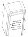
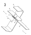
- the plug-side end 12 is designed for plug-in connection or mating with a complementary plug connector (not shown), wherein at least one electrical contact between the plug connector according to the invention and the complementary plug connector is to be produced.
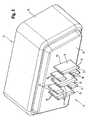
- at least one pair of contact elements made of an electrically conductive material with a first contact element 18 and a second contact element 20 is provided in the housing 10, as shown Fig. 3 seen.
- a pair of these contact elements 18, 20 are shown, however, the exemplary embodiment has seven such pairs.
- the storage and management of the contact element 18, 20 in the housing 10 is not shown for reasons of clarity in all figures.
- the first contact element 18 has a free end 22, which faces the plug-side end 12. At one end face of the free end 22, a completely covering end cap 24 made of an electrically insulating material is arranged.
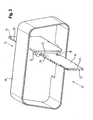
- the respective first contact element 18 of a pair is movable relative to the housing 10 and the second contact element 20 between a first position, as in FIG Fig. 1 and 5 represented, and a second position, as in Fig. 2 and 4 shown, movable.
- the second contact element 20 is arranged fixed with respect to the housing 10.
- a mechanism for moving the first contact elements 18 for reasons of clarity is not shown.
- the first position the first contact element 18 is retracted into a space bounded by the housing 10 and the cover 16.
- the first contact element 12 is pushed out of the housing 10 through a respective opening 26 in the cover 16 and projects beyond the cover 24 or the housing 10 in the direction of the plug-side end 12.
- the first contact elements 18 are extended from the first position through the cover 16 into the second position, so that the first contact elements 18 of each pair electrically contact corresponding contact elements in the complementary connector , Conversely, before pulling back again from the connector according to the invention and the complementary connector, the first contact elements 18 are withdrawn from the second position back to the first position.
- a corresponding first securing mechanism is provided, which only allows a movement of the first contact elements 18 from the first position to the second position when the connector according to the invention is fully inserted into the complementary connector.
- a second securing mechanism is preferably provided, which prevents disassembly of the connector according to the invention and the complementary connector, as long as the first contact elements 18 are outside the first position.
- the connector according to the invention is connected at its cable end 14 with at least one electrically conductive cable.
- fixed second contact element 20 is provided as in Fig. 3 to 5 shown. In the Fig. 3 to 5 For reasons of better clarity, only one pair of first and second contact elements 18, 20 is shown.
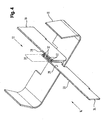
- the first contact element 18 and the second contact element 20 of a pair are each plate-shaped and in each case a pair of first and second contact element 18, 20 are arranged parallel to each other such that respective wide sides 28 of the first and second contact element 18, 20 facing each other. Furthermore, in an overlapping area 30 (FIG. Fig. 4 and 5 ) between the plate-shaped contact elements 18, 20 of a pair of first and second contact element 18, 20 arranged at least one coil spring 32 made of an electrically conductive and resilient material.
- a diameter of the coil spring 32 and a spacing of the plate-shaped contact elements 18, 20 and the wide sides 28 of a pair of first and second contact elements 18, 20 in the overlap region 30 is selected such that respective screw turns of the coil spring 32 with a first radial outside the first contact element 18 and with a second outer side opposite the first radial outer side abut the second contact element 20, so that between the turns of the coil spring 32 and the respective contact element 18, 20 results in an electrical contact point with contact surface and contact pressure.
- the contact pressure adjusts itself in that the turns of the helical spring 32 are deflected out of a respective rest position relative to a longitudinal axis of the helical spring 32 or are tilted relative to the longitudinal axis of the helical spring 32. This is achieved in that a distance of the plate-shaped contact elements 18, 20 of a pair of first and second contact element 18, 20 is smaller than an outer diameter of the coil spring 32nd
- the coil spring 32 is attached to the first contact element 18, so that the coil spring 32 moves with the first contact element 18. Accordingly, the turns of the helical spring 38 grind along the second contact element upon movement of the first contact element 18 20 and thereby maintain a sufficient electrical connection between the two contact elements 18, 20 upright.
- the second contact elements 20 each have a free end with an end face 34, this free end facing the cable end 14 of the connector according to the invention.
- the front end face 34 serves, for example, for electrical contacting with a wire or electrical line of a cable to be connected to the connector according to the invention.
- the helical spring 32 is preferably annular and defines within this ring an area space. This surface is aligned at the boundaries of the coil spring 32 parallel to a longitudinal axis of the coil spring 32 at the appropriate location. Due to the annular design of the coil spring 32, this forms in principle a torus in space, which has two opposite axial end sides. According to the invention, the helical spring 32 is arranged in the overlapping region 30 between the two contact elements 18, 20 such that the helical spring 32 strikes the second contact element 20 with turns at one axial end on the first contact element 18 and with turns on the other, opposite axial end , like out Fig. 3 seen.
- annular coil springs 32 are not fully illustrated due to the cut.
- the ring or in this limited area surrounds the first contact element 18 on the narrow side of the plate-like configuration of the first contact element 18.
- four coil springs 32 are provided.
- any other number may also be provided in an overlapping region 30 of a pair 18, 20, such as one, two, three, five or six coil springs 32.
Description
- Die vorliegende Erfindung betrifft einen Steckverbinder, insbesondere Ladestecker oder Hochstromstecker, mit einem Gehäuse aus einem elektrisch isolierenden Werkstoff und mit mindestens einem in dem Gehäuse angeordneten ersten Kontaktelement aus einem elektrisch leitenden Werkstoff, wobei das Gehäuse ein steckseitiges Ende aufweist, welches zum steckenden Verbinden mit einem komplementären Steckverbinder ausgebildet ist, sowie ein kabelseitiges Ende aufweist, welches zum elektrischen und mechanischen Verbinden mit einem elektrisch leitenden Kabel ausgebildet ist, und wobei das mindestens eine erste Kontaktelement ein freies Ende aufweist, welches dem steckseitigen Ende zugewandt ist, gemäß dem Oberbegriff des Anspruchs 1.
- Aus der
DE 20 2010 010 827 U1 ist ein Hochstromsteckverbinder zum Übertragen von elektrischen Strömen bekannt. Dieser weist ein Gehäuse aus elektrisch leitendem Werkstoff auf, welches zum mechanischen und elektrischen Verbinden mit einem Kabel ausgebildet ist und eine offene Seite zum Einstecken eines Gegensteckverbinders aus einem elektrisch leitenden Werkstoff aufweist. Weiterhin ist ein Kontaktelement vorgesehen, das im Gehäuse derart angeordnet und ausgebildet ist, dass es einen elektrischen Kontakt mit Kontaktfläche und Kontaktdruck zwischen dem Gehäuse und dem hierin eingesteckten Gegensteckverbinder herstellt. Das Kontaktelement weist wenigstens eine ringförmige Schraubenfeder auf. - Der Erfindung liegt die Aufgabe zugrunde, einen Steckverbinder der o.g. Art dahingehend zu verbessert, dass gegeneinander bewegliche Kontakte innerhalb des Steckverbinders möglich sind.
- Diese Aufgabe wird erfindungsgemäß durch einen Steckverbinder der o.g. Art mit den in Anspruch 1 gekennzeichneten Merkmalen gelöst. Vorteilhafte Ausgestaltungen der Erfindung sind in den weiteren Ansprüchen beschrieben.
- Bei einem Steckverbinder der o.g. Art ist es erfindungsgemäß vorgesehen, dass mindestens ein mit dem ersten Kontaktelement elektrisch leitend verbundenes zweites Kontaktelement aus einem elektrisch leitenden Werkstoff in dem Gehäuse angeordnet ist, wobei das erste Kontaktelement einen ersten plattenförmigen Abschnitt aufweist und das zweite Kontaktelement einen zweiten plattenförmigen Abschnitt aufweist, wobei das zweite Kontaktelement ein dem kabelseitigen Ende des Steckverbinders zugewandtes Ende aufweist, welches zum elektrischen Verbindern mit dem Kabel ausgebildet ist, wobei die plattenförmigen Abschnitte der beiden Kontaktelement parallel zueinander und einander zugewandt derart angeordnet sind, dass sich die plattenförmigen Abschnitte in Richtung senkrecht zu diesen in einem Überlappungsbereich mindestens teilweise überlappen und um einen vorbestimmten Abstand voneinander entfernt sind, wobei zum elektrisch leitenden Verbinden des ersten Kontaktelementes mit dem zweiten Kontaktelement zwischen den einander zugewandten plattenförmigen Abschnitten in dem Überlappungsbereich mindestens eine Schraubenfeder aus einem elektrisch leitenden und federelastischen Werkstoff vorgesehen ist, welche das erste Kontaktelement in dem ersten plattenförmigen Abschnitt an mindestens einer ersten Kontaktfläche mit einem ersten Kontaktdruck elektrisch kontaktiert und das zweite elektrische Kontaktelement in dem zweiten plattenförmigen Abschnitt an mindestens einer zweiten Kontaktfläche mit einem zweiten Kontaktdruck elektrisch kontaktiert.
- Dies hat den Vorteil, dass man das erste Kontaktelement relativ zum Gehäuse und zum zweiten Kontaktelement bewegen kann, ohne dass dabei der elektrische Kontakt zwischen den beiden Kontaktelementen negativ beeinflusst wird. Hierdurch ist die elektrische Kontaktstelle besonders zur Übertragung von hohen elektrischen Strömen, beispielsweise mit einer Stromstärke von 100 bis 400 A oder mehr, geeignet und kann durch das bewegliche erste Kontaktelement gleichzeitig mit einem Berührschutz für die elektrischen Kontakte des Steckverbinders ausgestattet werden.
- Eine besonders guten elektrische Kontakt durch einen hohen Kontaktdruck erzielt man dadurch, dass die Schraubenfeder schräggewickelte Windungen aufweist.
- Eine besonders hohe Anzahl von Kontaktflächen mit entsprechender Verbesserung der elektrischen Eigenschaften des Steckverbinders erzielt man dadurch, dass die Schraubenfeder ringförmig ausgebildet ist.
- Eine besonders gleichmäßige Verteilung das Kontaktdruckes auf die Kontaktflächen erzielt man dadurch, dass die ringförmige Schraubenfeder zwischen den beiden plattenförmigen Abschnitten in dem Überlappungsbereich derart angeordnet ist, dass mindestens ein Abschnitt einer ersten axiale Seite der ringförmigen Schraubenfeder den ersten plattenförmigen Abschnitt elektrisch und mechanisch kontaktiert sowie mindestens ein Abschnitt einer der ersten axialen Seite gegenüberliegende zweiten axialen Seite der Schraubenfeder den zweiten plattenförmigen Abschnitt elektrisch und mechanisch kontaktiert.
- Eine besonders hohe Zahl von Kontaktflächen zwischen der Schraubenfeder und den plattenförmigen Abschnitten der Kontaktelemente in dem Überlappungsbereich erzielt man dadurch, dass die ringförmige Schraubenfeder innerhalb des Ringes eine Fläche im Raum begrenzt, wobei die Fläche an der Grenze zur Schraubenfeder parallel zu einer Längsachse der Schraubenfeder steht, wobei die Schraubenfeder derart angeordnet ist, dass diese Fläche mindestens teilweise zwischen den und parallel zu den plattenförmigen Abschnitten in dem Überlappungsbereich angeordnet ist.
- Eine mechanisch besonders gute Fixierung der Schraubenfeder an dem ersten Kontaktelement erzielt man dadurch, dass die Schraubenfeder derart angeordnet ist, dass die Fläche das erste Kontaktelement teilweise umgreift.
- Eine weitere Erhöhung des Kontaktdruckes mit entsprechender Verbesserung der elektrischen Eigenschaften des Steckverbinders durch ein Verkippen der Windungen der Schraubenfeder relativ zu einer Längsachse der Schraubnefeder erzielt man dadurch, dass ein Abstand zwischen den plattenförmigen Abschnitten der Kontaktelemente kleiner ausgebildet ist, als ein Außendurchmesser der Schraubenfeder.
- Die Erfindung wird im Folgenden anhand der Zeichnung näher erläutert. Diese zeigt in:
- Fig. 1
- eine bevorzugte Ausführungsform eines erfindungsgemäßen Steckverbinders in einem Zustand mit eingefahrenen Kontaktelementen in perspektivischer Ansicht,
- Fig. 2
- den Steckverbinder gemäß
Fig. 1 in einem Zustand mit vollständig ausgefahrenen Kontaktelementen in perspektivischer Ansicht, - Fig. 3
- den Steckverbinder gemäß
Fig. 1 in teilweise aufgebrochener, perspektivischer Ansicht, - Fig. 4
- den Steckverbinder gemäß
Fig. 1 mit einem ersten Kontaktelement in einer zweiten, ausgefahrenen Position und - Fig. 5
- den Steckverbinder gemäß
Fig. 1 mit einem ersten Kontaktelement in einer ersten, eingefahrenen Position. - Die in den
Fig. 1 bis 5 dargestellte, bevorzugte Ausführungsform eines erfindungsgemäßen Steckverbinders umfasst ein Gehäuse 10 mit einem steckseitigen Ende 12 und einem kabelseitigen Ende 14. An dem Gehäuse 10 ist am steckseitigen Ende 12 eine Abdeckung 16 vorgesehen. Das steckseitige Ende 12 ist zum steckenden Verbinden bzw. Zusammenstecken mit einem komplementären Steckverbinder (nicht dargestellt) ausgebildet, wobei mindestens ein elektrischer Kontakt zwischen dem erfindungsgemäßen Steckverbinder und dem komplementären Steckverbinder hergestellt werden soll. Hierzu ist in dem Gehäuse 10 mindestens ein Paar von Kontaktelementen aus einem elektrisch leitenden Werkstoff mit einem ersten Kontaktelement 18 und einem zweiten Kontaktelement 20 vorgesehen, wie ausFig. 3 ersichtlich. InFig. 3 ist lediglich aus Gründen einer besseren Übersichtlichkeit ein Paar dieser Kontaktelemente 18, 20 dargestellt, jedoch weist die beispielhafte Ausführungsform sieben solcher Paare auf. Auch die Lagerung und Führung der Kontaktelement 18, 20 in dem Gehäuse 10 ist aus Gründen einer besseren Übersichtlichkeit in allen Fig. nicht dargestellt. Das erste Kontaktelement 18 weist eine freies Ende 22 auf, welches dem steckseitigen Ende 12 zugewandt ist. An einer Stirnseite des freien Endes 22 ist eine diese vollständig bedeckende Endkappe 24 aus einem elektrisch isolierenden Werkstoff angeordnet. - Das jeweilige erste Kontaktelement 18 eines Paares ist bezüglich des Gehäuses 10 und des zweiten Kontaktelementes 20 bewegbar zwischen einer ersten Position, wie in
Fig. 1 und5 dargestellt, und einer zweiten Position, wie inFig. 2 und4 dargestellt, bewegbar. Das zweite Kontaktelement 20 ist bezüglich des Gehäuses 10 feststehend angeordnet. In den Fig. ist eine Mechanik zum Bewegen der ersten Kontaktelemente 18 aus Gründen der besseren Übersichtlichkeit nicht dargestellt. In der ersten Position ist das erste Kontaktelement 18 in einen von dem Gehäuse 10 und der Abdeckung 16 begrenzten Raum zurückgezogen. In der zweiten Position ist das erste Kontaktelement 12 durch eine jeweilige Durchbrechungen 26 in der Abdeckung 16 hindurch aus dem Gehäuse 10 herausgeschoben und überragt dementsprechend die Abdeckung 24 bzw. das Gehäuse 10 in Richtung des steckseitigen Endes 12. - In der ersten Position ist somit ein Schutz vor einer unerwünschten Berührung der ersten Kontaktelemente 18 durch eine Bedienungsperson gegeben, wenn der erfindungsgemäße Steckverbinder nicht in einen komplementären Steckverbinder eingesteckt und damit das steckseitige Ende 12 frei zugänglich ist. An dem steckseitigen Ende 12 liegen lediglich die elektrisch isolierende Abdeckung 16 bzw. das elektrisch isolierende Gehäuse 10 sowie die Endkappen 24 frei. Somit kann auch im ungesteckten Zustand des erfindungsgemäßen Steckverbinders eine elektrische Spannung an den ersten Kontaktelementen 18 anliegen, ohne dass dabei eine Gefahr für eine Bedienungsperson durch ungewollte Berührung der ersten Kontaktelemente 18 an einer elektrisch leitenden Stelle ausgeht.
- Nachdem der erfindungsgemäße Steckverbinder mit einem komplementären Steckverbinder zusammen gesteckt ist, werden die ersten Kontaktelemente 18 aus der ersten Position heraus durch die Abdeckung 16 hindurch in die zweite Position ausgefahren, so dass die ersten Kontaktelemente 18 eines jeden Paares entsprechende Kontaktelemente in dem komplementären Steckverbinder elektrisch kontaktieren. Umgekehrt werden vor dem wieder Auseinanderziehen von dem erfindungsgemäßen Steckverbinder und dem komplementären Steckverbinder die ersten Kontaktelemente 18 aus der zweiten Position wieder in die erste Position zurückgezogen. Bevorzugt ist ein entsprechender erster Sicherungsmechanismus vorgesehen, welcher ein Bewegen der ersten Kontaktelemente 18 aus der ersten Position heraus in die zweite Position nur zulässt, wenn der erfindungsgemäße Steckverbinder vollständig in den komplementären Steckverbinder eingesteckt ist. Weiterhin ist bevorzugt ein zweiter Sicherungsmechanismus vorgesehen, welcher ein Auseinanderstecken von dem erfindungsgemäßen Steckverbinder und dem komplementären Steckverbinder verhindert, solange sich die ersten Kontaktelemente 18 außerhalb der ersten Position befinden.
- Der erfindungsgemäße Steckverbinder ist an seinem kabelseitigen Ende 14 mit mindestens einem elektrisch leitenden Kabel verbunden. Zur Entkopplung der Bewegung der ersten Kontaktelemente 18 von dem kabelseitigen Ende 14 bzw. dem Kabel ist zu jedem bewegbaren ersten Kontaktelement 18 das jeweils bezüglich des Gehäuses 10 feststehende zweite Kontaktelement 20 vorgesehen, wie in
Fig. 3 bis 5 dargestellt. In denFig. 3 bis 5 ist aus Gründen der besseren Übersichtlichkeit jeweils lediglich ein Paar aus erstem und zweitem Kontaktelement 18, 20 dargestellt. - Das erste Kontaktelement 18 und das zweite Kontaktelement 20 eines Paares sind jeweils plattenförmig ausgebildet und jeweils ein Paar aus erstem und zweitem Kontaktelement 18, 20 sind parallel zueinander derart angeordnet, dass jeweilige breite Seiten 28 von erstem und zweitem Kontaktelement 18, 20 einander zugewandt sind. Weiterhin ist in einem Überlappungsbereich 30 (
Fig. 4 und5 ) zwischen den plattenförmigen Kontaktelementen 18, 20 eines Paares aus erstem und zweitem Kontaktelement 18, 20 mindestens eine Schraubenfeder 32 aus einem elektrisch leitenden sowie federelastischen Werkstoff angeordnet. Ein Durchmesser der Schraubenfeder 32 und ein Abstand der plattenförmigen Kontaktelemente 18, 20 bzw. der breiten Seiten 28 eines Paares aus erstem und zweitem Kontaktelement 18, 20 in dem Überlappungsbereich 30 ist derart gewählt, dass jeweilige Schraubenwindungen der Schraubenfeder 32 mit einer ersten radialen Außenseite an dem ersten Kontaktelement 18 und mit einer der ersten radialen Außenseite gegenüberliegenden zweiten Außenseite an dem zweiten Kontaktelement 20 anliegen, so dass sich zwischen den Windungen der Schraubenfeder 32 und dem jeweiligen Kontaktelement 18, 20 eine elektrische Kontaktstelle mit Kontaktfläche und Kontaktdruck ergibt. Der Kontaktdruck stellt sich dadurch ein, dass die Windungen der Schraubenfeder 32 aus einer jeweiligen Ruheposition relativ zu einer Längsachse der Schraubenfeder 32 ausgelenkt bzw. relativ zur Längsachse der Schraubenfeder 32 verkippt werden. Dies wird dadurch erzielt, dass ein Abstand der plattenförmigen Kontaktelemente 18, 20 eines Paares aus erstem und zweitem Kontaktelement 18, 20 kleiner ist als ein Außendurchmesser der Schraubenfeder 32. - Die Schraubenfeder 32 ist an dem ersten Kontaktelement 18 befestigt, so dass sich die Schraubenfeder 32 mit dem ersten Kontaktelement 18 mitbewegt. Dementsprechend schleifen die Windungen der Schraubenfeder 38 bei einer Bewegung des ersten Kontaktelementes 18 entlang des zweiten Kontaktelementes 20 und halten dadurch eine ausreichende elektrische Verbindung zwischen den beiden Kontaktelementen 18, 20 aufrecht.
- Die zweiten Kontaktelemente 20 weisen jeweils ein freies Ende mit einer stirnseitigen Endfläche 34 auf, wobei dieses freie Ende dem kabelseitigen Ende 14 des erfindungsgemäßen Steckverbinders zugewandt ist. Die stirnseitige Endfläche 34 dient beispielsweise zum elektrischen Kontaktieren mit einer Ader oder elektrischen Leitung eines mit dem erfindungsgemäßen Steckverbinder zu verbindenden Kabels.
- Die Schraubenfeder 32 ist bevorzugt ringförmig ausgebildet und begrenzt innerhalb dieses Ringes eine Fläche Raum. Diese Fläche ist an den Grenzen zur Schraubenfeder 32 parallel zu einer Längsachse der Schraubenfeder 32 an der entsprechenden Stelle ausgerichtet. Durch die ringförmige Ausbildung der Schraubenfeder 32 bildet dieser im Prinzip einen Torus im Raum aus, welcher zwei gegenüberliegende axiale Endseiten aufweist. Erfindungsgemäß ist die Schraubenfeder 32 derart in dem Überlappungsbereich 30 zwischen den beiden Kontaktelementen 18, 20 angeordnet, dass die Schraubenfeder 32 mit Windungen an einem axialen Ende an dem ersten Kontaktelement 18 und mit Windungen an dem anderen, gegenüberliegenden axialen Ende an dem zweiten Kontaktelement 20 anschlägt, wie aus
Fig. 3 ersichtlich. Mit anderen Worten greift keines der Kontaktelemente 18, 20 durch die Fläche in dem Ring der ringförmigen Schraubenfeder 32 hindurch, sondern die elektrische Kontaktierung zwischen der Schraubenfeder 32 und den Kontaktelementen 18, 20 erfolgt an axialen Endseiten der ringförmigen Schraubenfeder 32. Hierdurch kann die Schraubenfeder 32 an dem ersten Kontaktelement 18 sicher befestigt werden und ist gegen ein Verrutschen oder Verwinden bei einer Bewegung des ersten Kontaktelementes 18 relativ zum zweiten Kontaktelement 20 gesichert. Wie weiterhin ausFig. 3 ersichtlich, umgreift die in dem Ring der Schraubenfeder 32 umschlossene Fläche teilweise das erste Kontaktelement 18. Dies unterstützt zusätzlich die Fixierung der Schraubenfeder 32 nicht nur an dem Ort des ersten Kontaktelementes 18 sondern auch gegen eine Verformung der ringförmigen Anordnung der Schraubenfeder 32 zwischen den Kontaktelementen 18, 20. - In
Fig. 4 und5 sind die ringförmigen Schraubenfedern 32 aufgrund des Schnittes nicht vollständig dargestellt. Der Ring bzw. die in diesem begrenzte Fläche umgreift das erste Kontaktelement 18 an der schmalen Seite der plattenförmigen Ausbildung des ersten Kontaktelementes 18. Gemäß der beispielhaften Darstellung vonFig. 4 und5 sind vier Schraubenfedern 32 vorgesehen. Es kann aber auch jede andere Anzahl in einem Überlappungsbereich 30 eines Paares 18, 20 vorgesehen sein, wie beispielsweise eine, zwei, drei, fünf oder sechs Schraubenfedern 32.
Claims (4)
- Steckverbinder, insbesondere Ladestecker oder Hochstromstecker, mit einem Gehäuse (10) aus einem elektrisch isolierenden Werkstoff und mit mindestens einem in dem Gehäuse angeordneten ersten Kontaktelement (18) aus einem elektrisch leitenden Werkstoff, wobei das Gehäuse ein steckseitiges Ende (12) aufweist, welches zum steckenden Verbinden mit einem komplementären Steckverbinder ausgebildet ist, sowie ein kabelseitiges Ende (14) aufweist, welches zum elektrischen und mechanischen Verbinden mit einem elektrisch leitenden Kabel ausgebildet ist, und wobei das mindestens eine erste Kontaktelement ein freies Ende aufweist, welches dem steckseitigen Ende zugewandt ist,
dadurch gekennzeichnet,
dass mindestens ein mit dem ersten Kontaktelement elektrisch leitend verbundenes zweites Kontaktelement (20) aus einem elektrisch leitenden Werkstoff in dem Gehäuse (10) angeordnet ist, wobei das erste Kontaktelement (18) einen ersten plattenförmigen Abschnitt aufweist und das zweite Kontaktelement (20) einen zweiten plattenförmigen Abschnitt aufweist, wobei das zweite Kontaktelement ein dem kabelseitigen Ende des Steckverbinders zugewandtes Ende aufweist, welches zum elektrischen Verbindern mit dem Kabel ausgebildet ist, wobei die plattenförmigen Abschnitte der beiden Kontaktelemente parallel zueinander und einander zugewandt derart angeordnet sind, dass sich die plattenförmigen Abschnitte in Richtung senkrecht zu diesen in einem Überlappungsbereich (30) mindestens teilweise überlappen und um einen vorbestimmten Abstand voneinander entfernt sind, wobei zum elektrisch leitenden Verbinden des ersten Kontaktelementes (18) mit dem zweiten Kontaktelement (20) zwischen den einander zugewandten plattenförmigen Abschnitten in dem Überlappungsbereich (30) mindestens eine Schraubenfeder (32) aus einem elektrisch leitenden und federelastischen Werkstoff vorgesehen ist, welche das erste Kontaktelement (18) in dem ersten plattenförmigen Abschnitt an mindestens einer ersten Kontaktfläche mit einem ersten Kontaktdruck elektrisch kontaktiert und das zweite elektrische Kontaktelement in dem zweiten plattenförmigen Abschnitt an mindestens einer zweiten Kontaktfläche mit einem zweiten Kontaktdruck elektrisch kontaktiert, wobei die Schraubenfeder (32) ringförmig ausgebildet ist, wobei die ringförmige Schraubenfeder (32) innerhalb des Ringes eine Fläche im Raum begrenzt, wobei die Fläche an der Grenze zur Schraubenfeder (32) parallel zu einer Längsachse der Schraubenfeder steht, wobei die Schraubenfeder derart angeordnet ist, dass diese Fläche mindestens teilweise zwischen den und parallel zu den plattenförmigen Abschnitten in dem Überlappungsbereich (30) angeordnet ist, wobei die Schraubenfeder derart angeordnet ist, dass die Fläche das erste Kontaktelement (18) teilweise umgreift. - Steckverbinder nach Anspruch 1, dadurch gekennzeichnet, dass die Schraubenfeder (32) schräggewickelte Windungen aufweist.
- Steckverbinder nach Anspruch 1 oder 2, dadurch gekennzeichnet, dass die ringförmige Schraubenfeder (32) zwischen den beiden plattenförmigen Abschnitten in dem Überlappungsbereich (30) derart angeordnet ist, dass mindestens ein Abschnitt einer ersten axiale Seite der ringförmigen Schraubenfeder (32) den ersten plattenförmigen Abschnitt elektrisch und mechanisch kontaktiert sowie mindestens ein Abschnitt einer der ersten axialen Seite gegenüberliegende zweiten axialen Seite der Schraubenfeder (32) den zweiten plattenförmigen Abschnitt elektrisch und mechanisch kontaktiert.
- Steckverbinder nach mindestens einem der vorhergehenden Ansprüche, dadurch gekennzeichnet, dass ein Abstand zwischen den plattenförmigen Abschnitten der Kontaktelemente (18, 20) kleiner ausgebildet ist, als ein Außendurchmesser der Schraubenfeder (32).
Applications Claiming Priority (2)
| Application Number | Priority Date | Filing Date | Title |
|---|---|---|---|
| DE202011005270U DE202011005270U1 (de) | 2011-04-14 | 2011-04-14 | Steckverbinder |
| PCT/EP2012/000426 WO2012139677A1 (de) | 2011-04-14 | 2012-01-31 | Steckverbinder |
Publications (2)
| Publication Number | Publication Date |
|---|---|
| EP2697867A1 EP2697867A1 (de) | 2014-02-19 |
| EP2697867B1 true EP2697867B1 (de) | 2014-09-03 |
Family
ID=44751900
Family Applications (1)
| Application Number | Title | Priority Date | Filing Date |
|---|---|---|---|
| EP12701983.4A Not-in-force EP2697867B1 (de) | 2011-04-14 | 2012-01-31 | Steckverbinder |
Country Status (9)
| Country | Link |
|---|---|
| US (1) | US8992265B2 (de) |
| EP (1) | EP2697867B1 (de) |
| JP (1) | JP5934779B2 (de) |
| KR (1) | KR101728783B1 (de) |
| CN (1) | CN103534877B (de) |
| CA (1) | CA2831455C (de) |
| DE (1) | DE202011005270U1 (de) |
| TW (1) | TWM435754U (de) |
| WO (1) | WO2012139677A1 (de) |
Families Citing this family (1)
| Publication number | Priority date | Publication date | Assignee | Title |
|---|---|---|---|---|
| JP6780513B2 (ja) * | 2017-01-18 | 2020-11-04 | 株式会社オートネットワーク技術研究所 | 端子モジュール |
Family Cites Families (13)
| Publication number | Priority date | Publication date | Assignee | Title |
|---|---|---|---|---|
| US3793606A (en) * | 1973-01-02 | 1974-02-19 | Ite Imperial Corp | Squeeze coil spring and current transfer means |
| JP3634074B2 (ja) * | 1996-06-28 | 2005-03-30 | 日本発条株式会社 | 導電性接触子 |
| JPH10189087A (ja) * | 1996-12-25 | 1998-07-21 | Nec Yamagata Ltd | ポゴピン |
| JP2002170624A (ja) * | 2000-11-30 | 2002-06-14 | Mitsubishi Electric Corp | 二股交流電源ケーブル |
| JP3767810B2 (ja) * | 2001-04-27 | 2006-04-19 | 株式会社ヨコオ | スプリングコネクタ |
| US6685492B2 (en) * | 2001-12-27 | 2004-02-03 | Rika Electronics International, Inc. | Sockets for testing electronic packages having contact probes with contact tips easily maintainable in optimum operational condition |
| US6814626B2 (en) * | 2002-10-21 | 2004-11-09 | L & K Precision Industry Co., Ltd. | Electrical connector for chargeable battery |
| US6758682B1 (en) * | 2003-02-13 | 2004-07-06 | Itt Manufacturing Enterprises, Inc. | Pogo contact |
| JP2004247170A (ja) * | 2003-02-13 | 2004-09-02 | Smk Corp | 押圧式スプリングコネクタ |
| US6776668B1 (en) * | 2003-08-01 | 2004-08-17 | Tyco Electronics Corporation | Low profile coaxial board-to-board connector |
| DE102008029505A1 (de) * | 2008-06-23 | 2009-12-31 | Otto Bock Healthcare Products Gmbh | Kontaktierungseinrichtung |
| DE102010032431A1 (de) | 2010-07-28 | 2011-04-21 | Daimler Ag | Verfahren zum Betreiben einer Verbrennungskraftmaschine |
| DE202010010827U1 (de) | 2010-07-29 | 2010-10-21 | Rosenberger Hochfrequenztechnik Gmbh & Co. Kg | Hochstromsteckverbinder |
-
2011
- 2011-04-14 DE DE202011005270U patent/DE202011005270U1/de not_active Expired - Lifetime
-
2012
- 2012-01-31 WO PCT/EP2012/000426 patent/WO2012139677A1/de active Application Filing
- 2012-01-31 EP EP12701983.4A patent/EP2697867B1/de not_active Not-in-force
- 2012-01-31 US US14/111,663 patent/US8992265B2/en not_active Expired - Fee Related
- 2012-01-31 CA CA2831455A patent/CA2831455C/en not_active Expired - Fee Related
- 2012-01-31 KR KR1020137030252A patent/KR101728783B1/ko not_active Application Discontinuation
- 2012-01-31 CN CN201280018371.1A patent/CN103534877B/zh not_active Expired - Fee Related
- 2012-01-31 JP JP2014504186A patent/JP5934779B2/ja not_active Expired - Fee Related
- 2012-03-12 TW TW101204419U patent/TWM435754U/zh not_active IP Right Cessation
Also Published As
| Publication number | Publication date |
|---|---|
| CN103534877B (zh) | 2016-04-06 |
| JP5934779B2 (ja) | 2016-06-15 |
| EP2697867A1 (de) | 2014-02-19 |
| TWM435754U (en) | 2012-08-11 |
| US20140073172A1 (en) | 2014-03-13 |
| CN103534877A (zh) | 2014-01-22 |
| CA2831455A1 (en) | 2012-10-18 |
| DE202011005270U1 (de) | 2011-09-01 |
| CA2831455C (en) | 2018-05-01 |
| JP2014511015A (ja) | 2014-05-01 |
| KR20140023990A (ko) | 2014-02-27 |
| KR101728783B1 (ko) | 2017-04-20 |
| US8992265B2 (en) | 2015-03-31 |
| WO2012139677A1 (de) | 2012-10-18 |
Similar Documents
| Publication | Publication Date | Title |
|---|---|---|
| EP3227970B1 (de) | Kontakthülse für einen elektrischen steckverbinder | |
| EP2599165B1 (de) | Hochstromsteckverbinder | |
| EP2690716B1 (de) | Elektrisches Anschlusselement | |
| EP3420612B1 (de) | Elektrischer steckverbinder | |
| WO2011113594A1 (de) | Hochstromsteckverbinder | |
| EP3396791B1 (de) | Aussenleiteranordnung | |
| EP2026417B1 (de) | Elektrischer Steckverbinder mit hermaphroditischen Kontaktelementen | |
| EP2797175B1 (de) | Stecker für ein mehrere Adern aufweisendes Daten- und/oder Telekommunikations-Kabel | |
| EP3516741B1 (de) | Stecker mit schutz | |
| EP3386033B1 (de) | Isolierkörper für eine steckverbindereinheit | |
| DE102015003935B3 (de) | Verbinder, Verfahren und Verwendung | |
| EP2345110B1 (de) | Steckverbinder für ein sternvierer-kabel | |
| EP2243198B1 (de) | Koaxialwinkelsteckverbinder | |
| DE102014105534A1 (de) | Buchsenkontakt und elektrische Steckverbindung | |
| DE202016100761U1 (de) | Kontaktelement für einen elektrischen Steckverbinder | |
| EP2697867B1 (de) | Steckverbinder | |
| DE19635260A1 (de) | Elektrische Mehrpol-Kontaktbuchse | |
| EP2697869B1 (de) | Steckverbinder mit einem kontaktelement | |
| DE112018005146T5 (de) | Elektrischer verbinderkörper vom hebeltyp und zugehörige elektrische verbinderanordnung | |
| DE102016006923B4 (de) | Koaxialsteckverbinder | |
| EP2942839B1 (de) | Steckverbinder mit niederiger steck- und hoher kontaktnormalkraft | |
| DE102021107137B4 (de) | Elektrischer Anschlussverbinder und elektrische Steckverbinderanordnung hierfür | |
| EP2192658B1 (de) | Verbindungseinrichtung | |
| DE102022118017A1 (de) | Reihung aus Steckverbindern | |
| DE1131768B (de) | Trennbare Kontaktvorrichtung fuer elektrische Steck- und Schaltverbindungen |
Legal Events
| Date | Code | Title | Description |
|---|---|---|---|
| PUAI | Public reference made under article 153(3) epc to a published international application that has entered the european phase |
Free format text: ORIGINAL CODE: 0009012 |
|
| 17P | Request for examination filed |
Effective date: 20131008 |
|
| AK | Designated contracting states |
Kind code of ref document: A1 Designated state(s): AL AT BE BG CH CY CZ DE DK EE ES FI FR GB GR HR HU IE IS IT LI LT LU LV MC MK MT NL NO PL PT RO RS SE SI SK SM TR |
|
| GRAP | Despatch of communication of intention to grant a patent |
Free format text: ORIGINAL CODE: EPIDOSNIGR1 |
|
| INTG | Intention to grant announced |
Effective date: 20140324 |
|
| DAX | Request for extension of the european patent (deleted) | ||
| GRAS | Grant fee paid |
Free format text: ORIGINAL CODE: EPIDOSNIGR3 |
|
| GRAA | (expected) grant |
Free format text: ORIGINAL CODE: 0009210 |
|
| AK | Designated contracting states |
Kind code of ref document: B1 Designated state(s): AL AT BE BG CH CY CZ DE DK EE ES FI FR GB GR HR HU IE IS IT LI LT LU LV MC MK MT NL NO PL PT RO RS SE SI SK SM TR |
|
| REG | Reference to a national code |
Ref country code: GB Ref legal event code: FG4D Free format text: NOT ENGLISH |
|
| REG | Reference to a national code |
Ref country code: AT Ref legal event code: REF Ref document number: 686011 Country of ref document: AT Kind code of ref document: T Effective date: 20140915 Ref country code: CH Ref legal event code: EP |
|
| REG | Reference to a national code |
Ref country code: IE Ref legal event code: FG4D Free format text: LANGUAGE OF EP DOCUMENT: GERMAN |
|
| REG | Reference to a national code |
Ref country code: CH Ref legal event code: NV Representative=s name: GACHNANG AG PATENTANWAELTE, CH |
|
| REG | Reference to a national code |
Ref country code: DE Ref legal event code: R096 Ref document number: 502012001200 Country of ref document: DE Effective date: 20141016 |
|
| REG | Reference to a national code |
Ref country code: SE Ref legal event code: TRGR |
|
| PG25 | Lapsed in a contracting state [announced via postgrant information from national office to epo] |
Ref country code: GR Free format text: LAPSE BECAUSE OF FAILURE TO SUBMIT A TRANSLATION OF THE DESCRIPTION OR TO PAY THE FEE WITHIN THE PRESCRIBED TIME-LIMIT Effective date: 20141204 Ref country code: LT Free format text: LAPSE BECAUSE OF FAILURE TO SUBMIT A TRANSLATION OF THE DESCRIPTION OR TO PAY THE FEE WITHIN THE PRESCRIBED TIME-LIMIT Effective date: 20140903 Ref country code: NO Free format text: LAPSE BECAUSE OF FAILURE TO SUBMIT A TRANSLATION OF THE DESCRIPTION OR TO PAY THE FEE WITHIN THE PRESCRIBED TIME-LIMIT Effective date: 20141203 Ref country code: ES Free format text: LAPSE BECAUSE OF FAILURE TO SUBMIT A TRANSLATION OF THE DESCRIPTION OR TO PAY THE FEE WITHIN THE PRESCRIBED TIME-LIMIT Effective date: 20140903 |
|
| REG | Reference to a national code |
Ref country code: NL Ref legal event code: VDEP Effective date: 20140903 |
|
| REG | Reference to a national code |
Ref country code: LT Ref legal event code: MG4D |
|
| PG25 | Lapsed in a contracting state [announced via postgrant information from national office to epo] |
Ref country code: HR Free format text: LAPSE BECAUSE OF FAILURE TO SUBMIT A TRANSLATION OF THE DESCRIPTION OR TO PAY THE FEE WITHIN THE PRESCRIBED TIME-LIMIT Effective date: 20140903 Ref country code: RS Free format text: LAPSE BECAUSE OF FAILURE TO SUBMIT A TRANSLATION OF THE DESCRIPTION OR TO PAY THE FEE WITHIN THE PRESCRIBED TIME-LIMIT Effective date: 20140903 Ref country code: LV Free format text: LAPSE BECAUSE OF FAILURE TO SUBMIT A TRANSLATION OF THE DESCRIPTION OR TO PAY THE FEE WITHIN THE PRESCRIBED TIME-LIMIT Effective date: 20140903 Ref country code: CY Free format text: LAPSE BECAUSE OF FAILURE TO SUBMIT A TRANSLATION OF THE DESCRIPTION OR TO PAY THE FEE WITHIN THE PRESCRIBED TIME-LIMIT Effective date: 20140903 |
|
| PG25 | Lapsed in a contracting state [announced via postgrant information from national office to epo] |
Ref country code: NL Free format text: LAPSE BECAUSE OF FAILURE TO SUBMIT A TRANSLATION OF THE DESCRIPTION OR TO PAY THE FEE WITHIN THE PRESCRIBED TIME-LIMIT Effective date: 20140903 |
|
| PG25 | Lapsed in a contracting state [announced via postgrant information from national office to epo] |
Ref country code: SK Free format text: LAPSE BECAUSE OF FAILURE TO SUBMIT A TRANSLATION OF THE DESCRIPTION OR TO PAY THE FEE WITHIN THE PRESCRIBED TIME-LIMIT Effective date: 20140903 Ref country code: PT Free format text: LAPSE BECAUSE OF FAILURE TO SUBMIT A TRANSLATION OF THE DESCRIPTION OR TO PAY THE FEE WITHIN THE PRESCRIBED TIME-LIMIT Effective date: 20150105 Ref country code: IS Free format text: LAPSE BECAUSE OF FAILURE TO SUBMIT A TRANSLATION OF THE DESCRIPTION OR TO PAY THE FEE WITHIN THE PRESCRIBED TIME-LIMIT Effective date: 20150103 Ref country code: CZ Free format text: LAPSE BECAUSE OF FAILURE TO SUBMIT A TRANSLATION OF THE DESCRIPTION OR TO PAY THE FEE WITHIN THE PRESCRIBED TIME-LIMIT Effective date: 20140903 Ref country code: RO Free format text: LAPSE BECAUSE OF FAILURE TO SUBMIT A TRANSLATION OF THE DESCRIPTION OR TO PAY THE FEE WITHIN THE PRESCRIBED TIME-LIMIT Effective date: 20140903 Ref country code: EE Free format text: LAPSE BECAUSE OF FAILURE TO SUBMIT A TRANSLATION OF THE DESCRIPTION OR TO PAY THE FEE WITHIN THE PRESCRIBED TIME-LIMIT Effective date: 20140903 |
|
| PG25 | Lapsed in a contracting state [announced via postgrant information from national office to epo] |
Ref country code: PL Free format text: LAPSE BECAUSE OF FAILURE TO SUBMIT A TRANSLATION OF THE DESCRIPTION OR TO PAY THE FEE WITHIN THE PRESCRIBED TIME-LIMIT Effective date: 20140903 |
|
| REG | Reference to a national code |
Ref country code: DE Ref legal event code: R097 Ref document number: 502012001200 Country of ref document: DE |
|
| PG25 | Lapsed in a contracting state [announced via postgrant information from national office to epo] |
Ref country code: BE Free format text: LAPSE BECAUSE OF NON-PAYMENT OF DUE FEES Effective date: 20150131 |
|
| PLBE | No opposition filed within time limit |
Free format text: ORIGINAL CODE: 0009261 |
|
| STAA | Information on the status of an ep patent application or granted ep patent |
Free format text: STATUS: NO OPPOSITION FILED WITHIN TIME LIMIT |
|
| PG25 | Lapsed in a contracting state [announced via postgrant information from national office to epo] |
Ref country code: DK Free format text: LAPSE BECAUSE OF FAILURE TO SUBMIT A TRANSLATION OF THE DESCRIPTION OR TO PAY THE FEE WITHIN THE PRESCRIBED TIME-LIMIT Effective date: 20140903 |
|
| 26N | No opposition filed |
Effective date: 20150604 |
|
| PG25 | Lapsed in a contracting state [announced via postgrant information from national office to epo] |
Ref country code: LU Free format text: LAPSE BECAUSE OF FAILURE TO SUBMIT A TRANSLATION OF THE DESCRIPTION OR TO PAY THE FEE WITHIN THE PRESCRIBED TIME-LIMIT Effective date: 20150131 |
|
| PG25 | Lapsed in a contracting state [announced via postgrant information from national office to epo] |
Ref country code: MC Free format text: LAPSE BECAUSE OF FAILURE TO SUBMIT A TRANSLATION OF THE DESCRIPTION OR TO PAY THE FEE WITHIN THE PRESCRIBED TIME-LIMIT Effective date: 20140903 |
|
| REG | Reference to a national code |
Ref country code: IE Ref legal event code: MM4A |
|
| PG25 | Lapsed in a contracting state [announced via postgrant information from national office to epo] |
Ref country code: SI Free format text: LAPSE BECAUSE OF FAILURE TO SUBMIT A TRANSLATION OF THE DESCRIPTION OR TO PAY THE FEE WITHIN THE PRESCRIBED TIME-LIMIT Effective date: 20140903 |
|
| REG | Reference to a national code |
Ref country code: FR Ref legal event code: PLFP Year of fee payment: 5 |
|
| PG25 | Lapsed in a contracting state [announced via postgrant information from national office to epo] |
Ref country code: IE Free format text: LAPSE BECAUSE OF NON-PAYMENT OF DUE FEES Effective date: 20150131 |
|
| PG25 | Lapsed in a contracting state [announced via postgrant information from national office to epo] |
Ref country code: MT Free format text: LAPSE BECAUSE OF FAILURE TO SUBMIT A TRANSLATION OF THE DESCRIPTION OR TO PAY THE FEE WITHIN THE PRESCRIBED TIME-LIMIT Effective date: 20140903 |
|
| REG | Reference to a national code |
Ref country code: FR Ref legal event code: PLFP Year of fee payment: 6 |
|
| PG25 | Lapsed in a contracting state [announced via postgrant information from national office to epo] |
Ref country code: BG Free format text: LAPSE BECAUSE OF FAILURE TO SUBMIT A TRANSLATION OF THE DESCRIPTION OR TO PAY THE FEE WITHIN THE PRESCRIBED TIME-LIMIT Effective date: 20140903 Ref country code: SM Free format text: LAPSE BECAUSE OF FAILURE TO SUBMIT A TRANSLATION OF THE DESCRIPTION OR TO PAY THE FEE WITHIN THE PRESCRIBED TIME-LIMIT Effective date: 20140903 Ref country code: HU Free format text: LAPSE BECAUSE OF FAILURE TO SUBMIT A TRANSLATION OF THE DESCRIPTION OR TO PAY THE FEE WITHIN THE PRESCRIBED TIME-LIMIT; INVALID AB INITIO Effective date: 20120131 |
|
| PG25 | Lapsed in a contracting state [announced via postgrant information from national office to epo] |
Ref country code: TR Free format text: LAPSE BECAUSE OF FAILURE TO SUBMIT A TRANSLATION OF THE DESCRIPTION OR TO PAY THE FEE WITHIN THE PRESCRIBED TIME-LIMIT Effective date: 20140903 |
|
| REG | Reference to a national code |
Ref country code: FR Ref legal event code: PLFP Year of fee payment: 7 |
|
| REG | Reference to a national code |
Ref country code: AT Ref legal event code: MM01 Ref document number: 686011 Country of ref document: AT Kind code of ref document: T Effective date: 20170131 |
|
| PGFP | Annual fee paid to national office [announced via postgrant information from national office to epo] |
Ref country code: FI Payment date: 20180129 Year of fee payment: 7 Ref country code: CH Payment date: 20180127 Year of fee payment: 7 |
|
| PG25 | Lapsed in a contracting state [announced via postgrant information from national office to epo] |
Ref country code: AT Free format text: LAPSE BECAUSE OF NON-PAYMENT OF DUE FEES Effective date: 20170131 |
|
| PG25 | Lapsed in a contracting state [announced via postgrant information from national office to epo] |
Ref country code: MK Free format text: LAPSE BECAUSE OF FAILURE TO SUBMIT A TRANSLATION OF THE DESCRIPTION OR TO PAY THE FEE WITHIN THE PRESCRIBED TIME-LIMIT Effective date: 20140903 |
|
| PG25 | Lapsed in a contracting state [announced via postgrant information from national office to epo] |
Ref country code: AL Free format text: LAPSE BECAUSE OF FAILURE TO SUBMIT A TRANSLATION OF THE DESCRIPTION OR TO PAY THE FEE WITHIN THE PRESCRIBED TIME-LIMIT Effective date: 20140903 |
|
| PGFP | Annual fee paid to national office [announced via postgrant information from national office to epo] |
Ref country code: FR Payment date: 20190128 Year of fee payment: 8 Ref country code: IT Payment date: 20190125 Year of fee payment: 8 Ref country code: GB Payment date: 20190130 Year of fee payment: 8 |
|
| PGFP | Annual fee paid to national office [announced via postgrant information from national office to epo] |
Ref country code: SE Payment date: 20190128 Year of fee payment: 8 |
|
| PGFP | Annual fee paid to national office [announced via postgrant information from national office to epo] |
Ref country code: DE Payment date: 20190401 Year of fee payment: 8 |
|
| REG | Reference to a national code |
Ref country code: CH Ref legal event code: PL |
|
| PG25 | Lapsed in a contracting state [announced via postgrant information from national office to epo] |
Ref country code: FI Free format text: LAPSE BECAUSE OF NON-PAYMENT OF DUE FEES Effective date: 20190131 |
|
| PG25 | Lapsed in a contracting state [announced via postgrant information from national office to epo] |
Ref country code: LI Free format text: LAPSE BECAUSE OF NON-PAYMENT OF DUE FEES Effective date: 20190131 Ref country code: CH Free format text: LAPSE BECAUSE OF NON-PAYMENT OF DUE FEES Effective date: 20190131 |
|
| REG | Reference to a national code |
Ref country code: DE Ref legal event code: R119 Ref document number: 502012001200 Country of ref document: DE |
|
| GBPC | Gb: european patent ceased through non-payment of renewal fee |
Effective date: 20200131 |
|
| REG | Reference to a national code |
Ref country code: SE Ref legal event code: EUG |
|
| PG25 | Lapsed in a contracting state [announced via postgrant information from national office to epo] |
Ref country code: DE Free format text: LAPSE BECAUSE OF NON-PAYMENT OF DUE FEES Effective date: 20200801 Ref country code: GB Free format text: LAPSE BECAUSE OF NON-PAYMENT OF DUE FEES Effective date: 20200131 Ref country code: SE Free format text: LAPSE BECAUSE OF NON-PAYMENT OF DUE FEES Effective date: 20200201 Ref country code: FR Free format text: LAPSE BECAUSE OF NON-PAYMENT OF DUE FEES Effective date: 20200131 |
|
| PG25 | Lapsed in a contracting state [announced via postgrant information from national office to epo] |
Ref country code: IT Free format text: LAPSE BECAUSE OF NON-PAYMENT OF DUE FEES Effective date: 20200131 |
|
| P01 | Opt-out of the competence of the unified patent court (upc) registered |
Effective date: 20230524 |