EP2681624B1 - Lithography system and method of processing substrates in such a lithography system - Google Patents
Lithography system and method of processing substrates in such a lithography system Download PDFInfo
- Publication number
- EP2681624B1 EP2681624B1 EP11802033.8A EP11802033A EP2681624B1 EP 2681624 B1 EP2681624 B1 EP 2681624B1 EP 11802033 A EP11802033 A EP 11802033A EP 2681624 B1 EP2681624 B1 EP 2681624B1
- Authority
- EP
- European Patent Office
- Prior art keywords
- substrate
- lithography
- lithography system
- unit
- substrates
- Prior art date
- Legal status (The legal status is an assumption and is not a legal conclusion. Google has not performed a legal analysis and makes no representation as to the accuracy of the status listed.)
- Active
Links
- 239000000758 substrate Substances 0.000 title claims description 261
- 238000001459 lithography Methods 0.000 title claims description 219
- 238000012545 processing Methods 0.000 title description 22
- 238000000034 method Methods 0.000 title description 14
- 238000012546 transfer Methods 0.000 claims description 61
- 238000002360 preparation method Methods 0.000 claims description 50
- 238000003860 storage Methods 0.000 claims description 39
- 238000000059 patterning Methods 0.000 claims description 12
- 230000009471 action Effects 0.000 description 49
- 239000002245 particle Substances 0.000 description 15
- 238000004519 manufacturing process Methods 0.000 description 11
- 235000012431 wafers Nutrition 0.000 description 11
- 230000008569 process Effects 0.000 description 8
- 238000013022 venting Methods 0.000 description 8
- 239000004065 semiconductor Substances 0.000 description 6
- 230000003750 conditioning effect Effects 0.000 description 5
- 238000011109 contamination Methods 0.000 description 5
- 239000000463 material Substances 0.000 description 5
- 230000009467 reduction Effects 0.000 description 4
- 238000003491 array Methods 0.000 description 3
- 238000010894 electron beam technology Methods 0.000 description 3
- 230000010354 integration Effects 0.000 description 3
- 239000007787 solid Substances 0.000 description 3
- 230000008878 coupling Effects 0.000 description 2
- 238000010168 coupling process Methods 0.000 description 2
- 238000005859 coupling reaction Methods 0.000 description 2
- 238000010586 diagram Methods 0.000 description 2
- 230000007257 malfunction Effects 0.000 description 2
- 230000003287 optical effect Effects 0.000 description 2
- 238000000206 photolithography Methods 0.000 description 2
- 238000005086 pumping Methods 0.000 description 2
- 239000000126 substance Substances 0.000 description 2
- 230000008901 benefit Effects 0.000 description 1
- 238000013016 damping Methods 0.000 description 1
- 238000009826 distribution Methods 0.000 description 1
- 238000005516 engineering process Methods 0.000 description 1
- 230000008014 freezing Effects 0.000 description 1
- 238000007710 freezing Methods 0.000 description 1
- 238000005286 illumination Methods 0.000 description 1
- 238000003780 insertion Methods 0.000 description 1
- 230000037431 insertion Effects 0.000 description 1
- 238000012423 maintenance Methods 0.000 description 1
- 238000012986 modification Methods 0.000 description 1
- 230000004048 modification Effects 0.000 description 1
- 238000003032 molecular docking Methods 0.000 description 1
- 229910000595 mu-metal Inorganic materials 0.000 description 1
- 238000007781 pre-processing Methods 0.000 description 1
- 230000001172 regenerating effect Effects 0.000 description 1
- 230000001105 regulatory effect Effects 0.000 description 1
Images


Classifications
-
- G—PHYSICS
- G03—PHOTOGRAPHY; CINEMATOGRAPHY; ANALOGOUS TECHNIQUES USING WAVES OTHER THAN OPTICAL WAVES; ELECTROGRAPHY; HOLOGRAPHY
- G03F—PHOTOMECHANICAL PRODUCTION OF TEXTURED OR PATTERNED SURFACES, e.g. FOR PRINTING, FOR PROCESSING OF SEMICONDUCTOR DEVICES; MATERIALS THEREFOR; ORIGINALS THEREFOR; APPARATUS SPECIALLY ADAPTED THEREFOR
- G03F7/00—Photomechanical, e.g. photolithographic, production of textured or patterned surfaces, e.g. printing surfaces; Materials therefor, e.g. comprising photoresists; Apparatus specially adapted therefor
- G03F7/70—Microphotolithographic exposure; Apparatus therefor
- G03F7/708—Construction of apparatus, e.g. environment aspects, hygiene aspects or materials
- G03F7/70808—Construction details, e.g. housing, load-lock, seals or windows for passing light in or out of apparatus
- G03F7/70825—Mounting of individual elements, e.g. mounts, holders or supports
-
- G—PHYSICS
- G03—PHOTOGRAPHY; CINEMATOGRAPHY; ANALOGOUS TECHNIQUES USING WAVES OTHER THAN OPTICAL WAVES; ELECTROGRAPHY; HOLOGRAPHY
- G03F—PHOTOMECHANICAL PRODUCTION OF TEXTURED OR PATTERNED SURFACES, e.g. FOR PRINTING, FOR PROCESSING OF SEMICONDUCTOR DEVICES; MATERIALS THEREFOR; ORIGINALS THEREFOR; APPARATUS SPECIALLY ADAPTED THEREFOR
- G03F7/00—Photomechanical, e.g. photolithographic, production of textured or patterned surfaces, e.g. printing surfaces; Materials therefor, e.g. comprising photoresists; Apparatus specially adapted therefor
- G03F7/70—Microphotolithographic exposure; Apparatus therefor
- G03F7/708—Construction of apparatus, e.g. environment aspects, hygiene aspects or materials
- G03F7/70975—Assembly, maintenance, transport or storage of apparatus
-
- H—ELECTRICITY
- H01—ELECTRIC ELEMENTS
- H01J—ELECTRIC DISCHARGE TUBES OR DISCHARGE LAMPS
- H01J37/00—Discharge tubes with provision for introducing objects or material to be exposed to the discharge, e.g. for the purpose of examination or processing thereof
- H01J37/02—Details
- H01J37/16—Vessels; Containers
-
- H—ELECTRICITY
- H01—ELECTRIC ELEMENTS
- H01J—ELECTRIC DISCHARGE TUBES OR DISCHARGE LAMPS
- H01J37/00—Discharge tubes with provision for introducing objects or material to be exposed to the discharge, e.g. for the purpose of examination or processing thereof
- H01J37/02—Details
- H01J37/18—Vacuum locks ; Means for obtaining or maintaining the desired pressure within the vessel
- H01J37/185—Means for transferring objects between different enclosures of different pressure or atmosphere
-
- H—ELECTRICITY
- H01—ELECTRIC ELEMENTS
- H01J—ELECTRIC DISCHARGE TUBES OR DISCHARGE LAMPS
- H01J2237/00—Discharge tubes exposing object to beam, e.g. for analysis treatment, etching, imaging
- H01J2237/30—Electron or ion beam tubes for processing objects
- H01J2237/317—Processing objects on a microscale
- H01J2237/3175—Lithography
- H01J2237/31774—Multi-beam
Definitions
- the present invention generally relates to a lithography system comprising a plurality of lithography system units.
- a very critical step in the manufacturing of integrated circuits on a wafer is lithography.
- a lithography process a predetermined pattern is transferred onto a semiconductor substrate, often referred to as a wafer.
- a wafer often referred to as a wafer.
- the smallest dimensions of structures patterned with a lithography apparatus are about 70 nm in size. However, to produce even faster circuits structures of smaller size are desired.
- lithography apparatuses developed to achieve such smaller wafer patterns can be integrated in current clean rooms without major adjustments to the equipment used in the circuit manufacturing process.
- newly developed higher resolution lithography apparatuses can replace the former lithography apparatuses without major adjustments in size, throughput and reliability.
- WO 2010/094804 A discloses a lithography apparatus arranged in a vacuum chamber, the vacuum chamber being provided with a door in its back wall.
- the present invention aims to provide a lithography system that meets the requirements set out above while permitting high throughput operation.
- the present invention provides a lithography system in which substrates can be handled and exposed both accurately and with sufficient throughput.
- the invention provides a lithography system unit according to claim 1 and lithography systems according to claims 8 and 13.
- the disclosure provides a lithography system comprising a plurality of lithography system units, each lithography system unit comprising: a lithography apparatus, for example a charged particle lithography apparatus, arranged in a vacuum chamber for patterning a substrate; a load lock system for transferring substrates into and out of the vacuum chamber; and a door for enabling entry into the vacuum chamber for servicing purposes; wherein the load lock system and the door of each lithography system unit are provided at the same side and face a free area at a side of the lithography system.
- a lithography apparatus for example a charged particle lithography apparatus
- the lithography system units including the lithography apparatuses within the vacuum chambers, are directly accessible from an area free of equipment providing a service area for the lithography system. Direct access simplifies servicing of the lithography system, and may reduce the downtime of the system or parts thereof.
- the lithography system units within the lithography system may be arranged back-to-back in two rows.
- the back-to-back layout of the lithography system units provides a lithography system with a limited "footprint”.
- Floor space within a fab is valuable, and efficient use of the fab floor space is important.
- the door may be removable connected to the vacuum chamber.
- a removably connected door enables easy and direct access to components within the vacuum chamber for servicing purposes. Easy access to these components can improve the servicing quality and may reduce the overall time needed for servicing. An easy way of removing the door would be to provide the door with one or more transfer elements, such as wheels or rails.
- the load lock system may be integrated into the door. Integrating the load lock system and the door to form a single unit reduces the amount of material used to manufacture the lithography system unit. The use of less material reduces the costs. Furthermore, in case the door is removably connected, the door is easier to handle.
- the lithography system unit may comprise a storage unit for temporary storage of substrates.
- the ability to temporarily store substrates enables the lithography system unit to continue operation in case of minor problems related to substrate supply and/or substrate processing in the lithography system unit.
- the lithography system may comprise a preparation system for preparing substrates for patterning in a lithography apparatus.
- the preparation of the substrates within the lithography system unit guarantees a relatively short distance between the location of preparation and the location of patterning. This short distance reduces risks related to contamination and the like. To shorten this distance even further, preferably, each lithography system unit comprises a preparation system.
- Transfer between the load lock system and the preparation system may be executed by means of a robot to reduce the risk of contamination even further.
- the preparation unit may include a clamping unit for clamping a substrate on a substrate structure to form a clamp.
- the lithography system further comprises a substrate supply system for supplying substrates to the lithography system; and a substrate transfer system for transferring the substrates between the substrate supply system and the plurality of lithography system units.
- a substrate supply system for supplying substrates to the lithography system
- a substrate transfer system for transferring the substrates between the substrate supply system and the plurality of lithography system units.
- the substrate supply system may be arranged to accommodate a substrate storage unit for temporary storage of substrates.
- the use of a substrate storage unit can reduce processing holdups within the lithography system due to temporary shortage of substrate supply and/or temporary lack of substrate removal of patterned substrates from the lithography system.
- the substrate storage unit may be a removable substrate storage unit, such as a front opening unified pod.
- the substrate supply system may be connectible to a track system. Connecting the substrate supply system to a track system improves the integration of the lithography system in a processing line within a semiconductor manufacturing environment.
- the substrate transfer system may be arranged above the lock systems of the lithography system units. Such positioning simplifies servicing of components within a lithography system unit without disturbing the operation of other lithography system units within the lithography system.
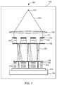
- FIG. 1 shows a simplified schematic drawing of an embodiment of a charged particle lithography apparatus 100.
- lithography systems are described for example in U.S. Patent Nos. 6,897,458 and 6,958,804 and 7,019,908 and 7,084,414 and 7,129,502 , U.S. patent application publication no. 2007/0064213 , and co-pending U.S. patent applications Serial Nos. 61/031,573 and 61/031,594 and 61/045,243 and 61/055,839 and 61/058,596 and 61/101,682 .
- the lithography apparatus 100 comprises an electron source 101 for producing an expanding electron beam 120.
- the expanding electron beam 120 is collimated by collimator lens system 102.
- the collimated electron beam 121 impinges on an aperture array 103, which blocks part of the beam to create a plurality of beamlets 122.
- the system generates a large number of beamlets 122, preferably about 10,000 to 1,000,000 beamlets.
- the electron beamlets 122 pass through a condenser lens array 104 which focuses the electron beamlets 122 in the plane of a beam blanker array 105, comprising a plurality of blankers for deflecting one or more of the electron beamlets.
- the deflected and undeflected electron beamlets 123 arrive at beam stop array 108, which has a plurality of apertures.
- the beamlet blanker array 105 and beam stop array 108 operate together to block or let pass the beamlets 123. If beamlet blanker array 105 deflects a beamlet, it will not pass through the corresponding aperture in beam stop array 108, but instead will be blocked. But if beamlet blanker array 105 does not deflect a beamlet, then it will pass through the corresponding aperture in beam stop array 108, and through beam deflector array 109 and projection lens arrays 110.
- Beam deflector array 109 provides for deflection of each beamlet 124 in the X and/or Y direction, substantially perpendicular to the direction of the undeflected beamlets, to scan the beamlets across the surface of target or substrate 130.
- the beamlets 124 pass through projection lens arrays 110 and are projected onto substrate 130.
- the projection lens arrangement preferably provides a demagnification of about 100 to 500 times.
- the beamlets 124 impinge on the surface of substrate 130 positioned on moveable stage 132 for carrying the substrate.
- the substrate usually comprises a wafer provided with a charged-particle sensitive layer or resist layer.
- the charged particle lithography apparatus 100 operates in a vacuum environment.
- a vacuum is desired to remove particles which may be ionized by the charged particle beams and become attracted to the source, may dissociate and be deposited onto the machine components, and may disperse the charged particle beams.
- a vacuum of at least 10 -6 bar is typically required.
- the charged particle lithography system is located in a vacuum chamber 140. All of the major elements of the lithography apparatus 100 are preferably housed in a common vacuum chamber, including the charged particle source, projector system for projecting the beamlets onto the substrate, and the moveable stage.
- the charged particle source environment is differentially pumped to a considerably higher vacuum of up to 10 -10 mbar.
- the source may be located in a separate chamber, i.e. a source chamber.
- Pumping down the pressure level in the source chamber may be performed in the following way. First, the vacuum chamber and the source chamber are pumped down to the level of the vacuum chamber. Then the source chamber is additionally pumped to a desired lower pressure, preferably by means of a chemical getter in a manner known by a skilled person.
- a chemical getter By using a regenerative, chemical and so-called passive pump like a getter, the pressure level within the source chamber can be brought to a lower level than the pressure level in the vacuum chamber without the need of a vacuum turbo pump for this purpose.
- the use of a getter avoids the interior or immediate outside vicinity of the vacuum chamber being submitted to acoustical and/or mechanical vibrations as would be the case if a vacuum turbo pump or similar would be used for such a purpose.
- FIG. 2a shows a simplified block diagram illustrating the principal elements of a modular lithography apparatus 200.
- the lithography apparatus 200 is preferably designed in a modular fashion to permit ease of maintenance.
- Major subsystems are preferably constructed in self-contained and removable modules, so that they can be removed from the lithography apparatus with as little disturbance to other subsystems as possible. This is particularly advantageous for a lithography machine enclosed in a vacuum chamber, where access to the machine is limited. Thus, a faulty subsystem can be removed and replaced quickly, without unnecessarily disconnecting or disturbing other systems.
- these modular subsystems include an illumination optics module 201 including the charged particle beam source 101 and beam collimating system 102, an aperture array and condenser lens module 202 including aperture array 103 and condenser lens array 104, a beam switching module 203 including beamlet blanker array 105, and projection optics module 204 including beam stop array 108, beam deflector array 109, and projection lens arrays 110.
- the modules are designed to slide in and out from an alignment frame.
- the alignment frame comprises an alignment inner subframe 205 and an alignment outer subframe 206.
- a frame 208 supports the alignment subframes 205 and 206 via vibration damping mounts 207.
- the substrate 130 rests on substrate support structure 209, which is in turn placed on a chuck 210.
- the chuck 210 sits on the stage short stroke 211 and long stroke 212.
- the lithography machine is enclosed in vacuum chamber 240, which may include a mu metal shielding layer or layers 215.
- the machine rests on base plate 220 supported by frame members 221.
- Each module requires a large number of electrical signals and/or optical signals, and electrical power for its operation.
- the modules inside the vacuum chamber 240 receive these signals from control systems which are typically located outside of the chamber 240.
- the vacuum chamber 240 includes openings, referred to as ports, for admitting cables carrying the signals from the control systems into the vacuum housing while maintaining a vacuum seal around the cables.
- Each module preferably has its collection of electrical, optical, and/or power cabling connections routed through one or more ports dedicated to that module. This enables the cables for a particular module to be disconnected, removed, and replaced without disturbing cables for any of the other modules.
- FIG. 2b schematically shows an assembly for removing and replacing a liftable module 272 in the lithography apparatus 200 of FIG. 2a in a relatively quick and easy way.
- the assembly comprises a module support structure provided with a track 260 for guiding a body 266 provided with a first wheel 267 and a second wheel 268.
- the body 266 comprises guiding wheels 273 for guiding and supporting the module 272.
- the track comprises portions forming substantially horizontal plateaus connected by portions forming ramps.
- the wheels 267, 268 are positioned such that the body 266 can translate vertically without rotation movement while the body 266 follows the track 260 with the wheels 267, 268 remaining in contact with the track 260.
- the body 260 advances over the track, it will translate both in the vertical direction as in the horizontal direction without any rotation. Consequently, a module 272 that is in contact with the body may be translated in a similar fashion.
- the assembly of FIG. 2b further comprises a movable cart 251 comprising guiding wheels 252 for guiding and supporting the module 272.
- the movable cart may further comprise adjusters 253 for adjusting the position and/or the orientation of the guiding wheels.
- the cart 251 may be provided with wheels 254, enabling the cart to be moved towards and from the support of the module 272.
- the position and/or the orientation of the guiding wheels 252 may be adjusted in order to align them with the guiding wheels 273 of the body.
- the cart 251 and the body 266 may be provided with a docking interface 255 in order to connect the cart 251 with the body 266.
- the module 272 After the module 272 is lifted, it may be moved along the guiding wheels of both the body 266 and the cart 251 onto the cart 251. The module 272 may then be moved away, while being carried by the movable cart 251.
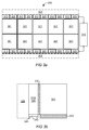
- FIG. 3a shows a top view of a layout of lithography system 300 comprising a group of lithography system units according to an embodiment of the invention.
- the layout may be referred to as lithography system 300 or cluster 300.
- FIG. 3b schematically shows a cross-sectional side view of a portion of the lithography system 300.
- the lithography system 300 comprises a group of ten lithography system units.
- the lithography system units are arranged back-to-back in two rows of five. Directly adjacent to the cluster 300, floor space is reserved as service area 305.
- Each lithography system unit comprises a lithography apparatus 301 that is contained in its own vacuum chamber, with one side of each vacuum chamber facing a lithography system unit in the other row, while the opposing side faces the surroundings of the cluster 300, in particular the service area 305.
- the vacuum chamber preferably comprises all elements that enable lithography processing, including a charged particle source, a projector system for projecting charged particle beamlets onto a substrate to be patterned, and a moveable substrate stage.
- the vacuum chamber may correspond to the chamber 240 discussed with reference to FIG. 2a .
- the side of the lithography system unit facing a free area provided for service purposes comprises a load lock system 310 for transferring substrates into and out of the vacuum chamber, and also comprises an access door 330 that can be opened for such service purposes.
- the lithography system units are provided with a door 330 at the same side as the load lock system 310.
- the door 330 may be removably attachable, and may be removable in its entirety, for example by using a transfer unit 340.
- the transfer unit 340 may be arranged to support the door 330 and may comprise one or more transfer elements 345, such as wheels or rails.
- the lithography apparatus 301 may be supported by a supporting structure 335 for positioning the lithography apparatus at an elevated position.
- the free area at the side at which the load lock system and access door are located preferably is sufficiently large to accommodate the footprint of the door and the load lock. Furthermore, it is desirable that the free area is sufficiently large to accommodate a footprint of an arrangement for carrying components of the lithography apparatus. For example, in case a cart such as cart 251 in FIG. 2b is used for transfer of a module, the free area is preferably sufficiently large to enable transfer of the module on the cart towards and away from the lithography system units.
- the lithography system 300 thus comprises a plurality of lithography system units having a load lock system 310 and a door 330 facing the surroundings, more in particular facing the service area 305 surrounding the lithography system 300. Due to the "outward" orientation of the load lock systems 310 and doors 330, the lithography system units, including the lithography apparatuses 301 within the vacuum chambers, are directly accessible from the service area 305. Direct access simplifies servicing of the lithography system 300, and may reduce the downtime of the lithography system or parts thereof. Opening a single specific vacuum chamber for servicing can be done without affecting the throughput of other lithographic system units within the lithography system 300.
- the back-to-back layout of the lithography system units provides a lithography system 300 with a limited "footprint”.
- Floor space within a fab is valuable, and efficient use of the fab floor space is thus important.
- the load lock system 310 may be integrated into the door 330. Integration of the load lock system 310 and the door 330 reduces the amount of material used in manufacturing the lithography system unit. A portion of the door 330 may be directly used as one of the side walls of the load lock system 310. The material reduction has the advantage that the door and load lock system combination is easier to handle during servicing. Furthermore, as less material is needed during manufacturing, the costs of manufacturing the lithography system are reduced as well.
- the lithography system 300 further comprises a substrate supply system 315.
- the substrate supply system 315 is arranged to receive substrates to be processed by the lithography system 300, and to provide these substrates to the lithography system units for processing. This can effectively mean that the substrate supply system 315 provides the substrates to a preparation system 320 for pre-processing purposes. After patterning, the substrate supply system 315 may collect the patterned substrates.
- the use of a substrate supply system 315 enables the lithography system 300 to efficiently cooperate with other equipment in the fab as it allows for a relatively easy replacement of presently used lithography systems.
- FIG. 3c schematically shows another side view of the lithography system 300 of FIG. 3a .
- the lithography system 300 further comprises a substrate transfer system 350 for receiving substrates from and/or sending substrates to the substrate supply system 315.
- the substrate transfer system 350 may take the form of a suitable conveyor system, for example a conveyor system which extends in a substantially horizontal direction.
- the substrate transfer system 350 is designed not to interfere with the doors 330 of the lithography system units. This may be accomplished as shown in FIG. 3c .
- the substrate transfer system 350 extends in a substantially horizontal direction, and is arranged above the load lock systems 310, as well as the preparation units 320, of the lithography system units.
- the door of a single lithography system unit within the lithography system 300 may be opened for servicing purposes while the substrate transfer system 350 can continue with the transfer of substrates between the substrate supply system 315 and the other lithography system units within the lithography system 300.
- the layout described with reference to FIGS. 3a-3c provides a cluster of lithography system units with limited complexity.
- the layout can be scaled rather easily. For example, if the lithography system 300 needs to operate with an 80% capacity, only eight out of the ten lithography system units need to be operational and/or installed.
- clamping is defined as providing a substrate on a substrate support structure to form a single structure, hereafter referred to as "clamp".
- clamped substrate is used to refer to a substrate being clamped to a substrate support structure.
- Pre-alignment relates to aligning the substrate and/or clamp such that patterning can be performed onto a predetermined portion of the substrate in a certain orientation.
- Pump down relates to the step of reducing the pressure surrounding the substrate to minimize contamination and to reduce the influence of the substrate on the vacuum chamber pressure upon insertion into the lithography apparatus 301.
- the substrate After the patterning action performed by the lithography apparatus 301, the substrate is typically exposed to a venting action, and an unclamping action, i.e. separating the substrate from the substrate support structure. In between the venting and unclamping actions, the substrate may be transferred.
- the load lock system 310 forms an interface to a vacuum environment within the vacuum chamber.
- the system 310 is typically used for the pump down action and the venting action described above.
- the load lock system 310 comprises one or more chambers in which the pressure can be regulated.
- the load lock system 310 may comprise a single chamber suitable for both pump down and venting actions.
- the system 310 comprises separate chambers for pump down and venting.
- the system 310 comprises pumps for pumping down the pressure within a chamber to a reduced pressure, e.g. a vacuum suitable for transfer of the clamped substrate and substrate support to the lithographic apparatus 301.
- the load lock system 310 comprises vents for venting a chamber to increase the pressure after processing of the clamped substrate in the lithographic apparatus 301.
- Clamping and/or unclamping may be performed in the preparation systems 320.
- the clamping may be performed at a different location prior to providing the substrate to the preparation systems 320, for example within the common supply system 315.
- clamping and/or unclamping may be performed within the load lock system 310.
- clamping unit refers to a unit for clamping and/or unclamping.
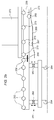
- FIG. 4a schematically shows a lithography system unit provided with a first load lock chamber 310a for pump down, a second load lock chamber 310b for venting and a preparation system 320 that includes a number of clamping units 360a-d.
- a clamp is formed in a suitable clamping unit 360a-d in the preparation system 320 and then inserted into the vacuum chamber via the first load lock chamber 310a. After patterning of the substrate by the lithography apparatus 301, the clamp is transferred back to a suitable clamping unit 360a-d in the preparation system 320 via the second load lock chamber 310b for unclamping.
- the preparation system 320 further includes a pre-alignment unit 370 for pre-aligning the substrate before entry into the lithography apparatus 301 via the first load lock chamber 310a.
- Pre-alignment may be needed to ensure that the position and/or orientation of the substrate on the substrate support structure are suitable for accurate exposure within the lithography apparatus 301.
- Pre-alignment may be performed on an individual substrate before the substrate is clamped. However, in such case the clamping must be done in an extremely precise and coordinated way.
- the substrate is pre-aligned while being clamped onto a substrate support structure. After pre-alignment in the pre-alignment unit 370 the substrate is provided to the first load lock chamber 310a for further processing.
- a preparation system 320 may further comprise one or more additional units.
- the preparation system 320 may include a conditioning unit for conditioning clamped substrates and/or unclamped substrates prior to exposure in the lithography apparatus 301.
- the conditioning unit may be arranged for thermal conditioning of a clamped or unclamped substrate by e.g. removing heat energy from the substrate (and substrate support structure) to improve the accuracy of lithographic patterning, as is known to persons skilled in the art.
- Substrates and/or clamps may be transferred between different units by using a robot that operates within a robot space 400.
- the robot comprises a carrier 401 that can move in a substantially vertical direction.
- the carrier 401 is arranged for suitably transporting substrates and/or clamps between the load lock chambers 310a, 310b, the clamp units 360a-d, and the pre-alignment unit 370.
- the robot 401 may further be arranged to handle substrate exchange with the substrate transfer system 350.
- a lithography system unit may further comprise a storage unit 410 for temporarily storing substrates.
- the stored substrate may be substrates that still need to be patterned by the lithography apparatus 301.
- the substrate storage unit 410 may be arranged to store patterned substrates awaiting transfer via the substrate transfer system 350.
- the storage unit 410 is coupled to the substrate transfer system 350.
- the storage unit 410 may be coupled to a replaceable unit and may take the form of a so-called front opening unified pod (FOUP).
- FOUPs enable relatively safe transfer of several substrates in one FOUP in a (clean room) environment.
- the storage unit 410 is a replaceable unit, for example a FOUP.
- FIG. 4a schematically shows that electronics 420 needed to ensure proper operation of the lithography apparatus 420 may be placed on top of the lithography apparatus 301.
- the door 330 can be removed together with the other components outside the vacuum chamber, for example by means of a transfer unit 340 comprising one or more transfer elements 345.
- FIG. 4b schematically shows an embodiment in which the substrate supply system 315 comprises a number of clamping units 360a-360z substantially placed on top of each other. Additionally, the substrate supply system 315 is suitably connected to a clamped substrate or clamp transfer system 350'.
- the substrate supply system 315 comprises a substrate handling robot that operates within a robot space 500.
- the robot is arranged for transporting substrates towards and away from the clamping unit 360a-360z.
- the robot comprises a carrier 501 that can move in a substantially vertical direction.
- the carrier 501 may be able to move in a substantially horizontal direction as well, for example to enable an exchange of unclamped substrates via an interface with an external system such as a track system as will be discussed with reference to FIGS. 5a, 5b .
- the carrier 501 may also be arranged for transporting clamps between the clamping units 360a-360z and the clamp transfer system 350'.
- the substrate supply system 315 may be provided with a supply and/or storage unit 510 for the supply and/or storage of substrates.
- the carrier 501 is arranged to arrange transport of clamps and/or substrates to and from the storage unit 510.
- the storage unit 510 arranged to store patterned substrates, also referred to as exposed substrates, collected by the substrate supply system 315 after processing in a lithography apparatus in a lithography system unit. Central distribution and collection of substrates enables an efficient integration of the lithography cluster in a fab process line.
- the supply and/or storage unit 510 may be a replaceable unit and may take the form of a so-called front opening unified pod (FOUP).
- FOUPs enable relatively safe transfer of several substrates in one FOUP in a (clean room) environment.
- FIGS. 4a, 4b Although different components in FIGS. 4a, 4b are shown on top of each other, alternative embodiments in which one or more of the components are positioned adjacent to each other in a substantially horizontal direction are envisioned as well. Furthermore, additional support units to enable transfer of substrates between the carrier 501 and a clamping unit 360a-360z may be present.
- clamping and/or unclamping is performed within the load lock system 310.
- Load lock systems 310 that are capable of executing these actions then need to be rather sophisticated in nature.
- Clamping methods include but are not limited to clamping by using capillary forces, for example as described in US-patent application 2010/0265486 assigned to the owner of the present invention, clamping by applying a vacuum, clamping by freezing the substrate to the substrate support structure, and clamping by the use of electromagnetic forces.
- the type of clamping may depend on the type of subsequent processing to be used on the substrate.
- a lithography system where the clamping and/or unclamping units are provided within the lithography system units, for example within a preparation system 320 as shown in FIG. 4a or within a load lock system 310, may be identified as a cluster 300 with a localized unclamped substrate supply, hereafter referred to as a localized cluster.
- a localized cluster unclamped substrates are transported to an area in close proximity of the lithography apparatus 301 in which they are to be processed. Then, the substrates are clamped on a substrate support structure, and finally the clamps, i.e. substrates clamped onto a substrate support structure, are provided to the lithography apparatus 301.
- a lithography system where the clamping and/or unclamping units are centrally provided, for example within the substrate supply system 315 as shown in FIG. 4b , may be referred to as a centralized cluster 300.
- a centralized cluster unclamped substrates are clamped at a central location. The clamp is then transferred further into the cluster for further processing by the plurality of lithography apparatuses 301.
- the number of components within a centralized cluster may be lower than the number of components within a localized cluster, in particular in case the clamping and unclamping units 360 are shared by all lithography system units 301 within the cluster 300.
- localized clusters can be scaled relatively easy, as addition and/or removal of a lithography system unit merely means that, at most, adjustments have to be made to the substrate transfer system.
- the footprint of the substrate supply system 315 is generally smaller than the footprint of a centralized cluster, provided the clusters comprise the same number of lithography system units. Such footprint reduction is particularly achieved in case the number of lithography system units within the lithography system 300 is limited.
- the load lock systems 310 may comprise one or more valves for creating a controlled pressure environment. Keeping the substrates and/or clamps in a controlled pressure environment permits a reduced contamination environment to be maintained around the substrates.
- the controlled pressure environment may be an intermediate vacuum, between atmospheric pressure and the high vacuum of the lithography apparatus 301. This intermediate vacuum enables a reduction of contamination while avoiding having a large volume maintained at a high vacuum. In particular in case of not yet patterned substrates the intermediate vacuum aids in preparing the substrate for later processing in the vacuum environment of the lithography apparatus.
- the substrate supply system 315 may be connected to other tools, such as a track system, in a semiconductor manufacturing environment for the exchange of substrates.
- FIGS. 5a, 5b schematically show two different ways of coupling a substrate supply system 315 to a track system 600.
- the track system 600 comprises two track process lines 610a, 610b, denoted by solid arrows.
- the track system 600 is provided with a substrate handler 620 for receiving substrates from track process lines 610a, 610b and forwarding these substrates to the lithography system 300 for processing.
- the substrate handler 620 is arranged for receiving patterned substrates from the lithography system 300 and forwarding these substrates to suitable process lines within the track, i.e. either track line 610a or 610b.
- the substrate supply system 315 comprises a substrate handler 520 for transferring substrates between the track system 600 and a substrate transfer system (denoted by dashed arrows).
- the substrate transfer between the substrate supply system 315 and the lithography system units is denoted by solid arrows.
- Such substrate transfer may be executed by any suitable substrate transfer system, for example the substrate transfer system 350 as depicted in and described with reference to FIGS. 3c and 4a or the clamp transfer system 350' as depicted in and described with reference to FIG. 4b .
- the substrate handler 520 within the substrate supply system 315 may take the form of a handler such as handler 501 as depicted in and described with reference to FIG. 4b .
- the track process lines 610a, 610b within the track system 600 are directly coupled to substrate supply system 315.
- the substrate supply system 315 now comprises two substrate handlers 520a, 520b, where the first substrate handler 520a is arranged to coordinate transfer between the track process line 610a and the lithography system, and the second substrate handler 520b is arranged to coordinate transfer between the track process line 610b and the lithography system.
- Both substrate handlers 520a, 520b may take the form of a robot, for example a robot comprising a carrier as described with reference to FIG. 4b .
- the substrate handlers 520a, 520b may further be arranged to coordinate substrate transfer within a portion of the substrate supply system 315.
- FIG. 6 schematically shows an action flow of a method of processing a substrate in a lithography system unit.
- the lithography system unit comprises a storage unit SU, a preparation system PS and a load lock LL.
- the storage unit SU may for example comprise the storage unit 410 described above
- the preparation system PS may for example comprise the preparation unit 320 described above
- the load lock LL may for example comprise the load lock system 310 described above.
- the load lock LL is connected to a lithography apparatus for exposing a pattern onto a target surface of a substrate to be exposed.
- the lithography system unit comprises a substrate handling robot, such as a robot comprising and/or taking the form of carrier 401 in FIG. 4a , for transferring substrates between different components within the lithography system unit.
- a substrate to be exposed is provided in action 601.
- Providing the substrate to the lithography system unit may be done using the combination of the substrate supply system 315 and substrate transfer system 350 shown in FIG. 3c .
- the substrate may be provided to the storage unit, as shown in FIG. 6 , but may also be placed on the robot, for example at an interface between the lithography system unit and the external supply arrangement, for example a substrate transfer system.
- the substrate may be directed towards a predetermined orientation prior to further actions. This type of "coarse” alignment alleviates further alignment procedures because the substrates to be exposed enter the exposure method with roughly the same orientation.
- the substrate is then transferred to a substrate preparation system PS in action 602 by the robot.
- the robot does not pick up the substrate from the storage unit SU as shown in FIG. 6 , but transfers the substrate to the preparation system PS after being provided with the substrate at an interface of the lithography system unit with an external supply arrangement.
- the substrate is at least clamped to a substrate support structure in action 603. Additionally, other pre-conditioning actions such as (further) alignment, may take place, preferably before the clamping action.
- the clamped substrate is then transferred by the robot to the load lock LL in action 604.
- the load lock LL is connected to the lithography apparatus, and the clamped substrate that is delivered by the robot accesses the lithography apparatus via the load lock LL.
- the clamped substrate is then exposed in the lithography apparatus in action 605.
- the substrate is transferred back to the load lock LL.
- the robot then transfers the exposed clamped substrate to the preparation system PS in action 606.
- the exposed substrate is separated from the substrate support structure in action 607. Finally, the separated exposed substrate is transferred by the robot to a point for removal from the lithography system unit in action 608.
- This point may be located in the storage unit SU, as schematically depicted in FIG. 6 . However, this point for removal may also be located at an interface of the lithography system unit with an external supply arrangement.
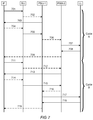
- FIG. 7 schematically shows another action flow for processing a substrate in a lithography system unit.
- Transfer of the substrate may be accomplished using a substrate handling robot, FIG. 7 illustrating the trajectory of the robot for making the sequence of transfers.
- the robot may comprise and/or take the form of a carrier such as carrier 401 in FIG. 4a .
- the interface between the substrate transfer system and the robot is denoted by "IF".
- the exemplary lithography system unit comprises a storage unit SU, a first preparation system unit PSU-1, a second preparation system unit PSU-2, and a load-lock LL coupled to a lithography apparatus.
- the interface IF may for example comprise the interface between the substrate transfer system 350 and the lithography system unit described above
- the storage unit SU may for example comprise the storage unit 410 described above
- the preparation units PSU-1 and PSU-2 may for example comprise two of the clamp units 360 described above
- the load lock LL may for example comprise the load lock system 310 described above. Movements during which the robot actually transfers a substrate are represented by the solid arrows. Mere movements of the robot without substrate transfer are denoted by the dashed arrows.
- the trajectory in FIG. 7 starts with the robot being positioned at the interface IF.
- the first movement involves the transfer of a new unclamped substrate to be exposed from the interface IF towards the storage unit SU for temporary storage in action 701.
- the robot moves towards the first preparation system unit PSU-1 in action 702.
- the robot picks up an exposed unclamped substrate and transfers this substrate in action 703 to the interface IF to allow removal thereof from the lithography system unit.
- the robot then moves back in action 704 to storage unit SU to pick up the unclamped substrate for exposure placed therein at the end of action 701.
- action 705 the unclamped substrate is picked up from the storage unit SU and transferred to the preparation system unit PSU-1.
- the robot moves in action 706 to the preparation system unit PSU-2.
- the robot picks up a clamped substrate to be exposed and transfers the clamped substrate to the load lock LL for exposure in the lithography apparatus in action 707.
- the robot picks up an exposed clamped substrate and transfers this substrate to preparation system unit PSU-2 for unclamping in action 708.
- the robot moves to the interface IF without carrying a substrate in action 709.
- the series of actions 701-709 is referred to as "cycle A".
- the trajectory in FIG. 7 then continues at the interface IF with action 711, which is similar to action 701.
- the robot does not move to preparation system unit PSU-1 as in action 702, but instead moves to preparation system unit PSU-2 in action 712.
- the robot picks up an exposed clamped substrate present in preparation system unit PSU-2, and transfers this substrate to the interface IF to enable removal of the substrate from the lithography system unit.
- the robot then moves to the storage unit SU in action 714 in a similar fashion as it did in action 704.
- the robot picks up an unclamped substrate to be exposed from the storage unit SU and transfers this substrate to the preparation system unit PSU-2 in action 715.
- the robot moves to the preparation system unit PSU-1 in action 716, picks up a clamped substrate to be exposed and transfers the clamped substrate to the load lock LL for exposure in the lithography apparatus in action 717. After removal of the clamped substrate at the load lock, the robot picks up an exposed clamped substrate and transfers this substrate to preparation system unit PSU-1 for unclamping in action 718. Finally, the robot moves to the interface IF without carrying a substrate in action 719.
- the series of actions 711-719 is referred to as "cycle B".
- the robot may now repeat the trajectory of FIG. 7 , which effectively means that it alternates between following cycle A and cycle B, where the difference between the two cycles is the role of the preparation system unit PSU-1 and the preparation system unit PSU-2.
- the trajectory shown in FIG. 7 is particularly useful to ensure a continuous flow of substrates in case the clamping action in a preparation system unit takes more time than the duration of an entire cycle.
- lithography system units comprising ten lithography system units
- the number of lithography system units within a lithography system may vary.
- any other number of lithography system units above one may be used.
Description
- The present invention generally relates to a lithography system comprising a plurality of lithography system units.
- In the semiconductor industry, an ever increasing desire to manufacture smaller structures with high accuracy and reliability puts great demands on wafer processing technology. In particular, it is important to maximize wafer throughput of wafer processing equipment while maintaining the lowest capital costs and operational costs, and without excessive use of floor space. Floor space in a semiconductor manufacturing environment is expensive, as most space needs to meet high standard clean room conditions. Therefore, the floor space that is to be occupied by wafer processing equipment, i.e. the so-called footprint, is preferably as limited as possible. Furthermore, to ensure that clean room conditions can be maintained, wafer processing equipment is preferably serviced within the clean room.
- A very critical step in the manufacturing of integrated circuits on a wafer is lithography. In a lithography process, a predetermined pattern is transferred onto a semiconductor substrate, often referred to as a wafer. Currently, the smallest dimensions of structures patterned with a lithography apparatus are about 70 nm in size. However, to produce even faster circuits structures of smaller size are desired.
- Replacement of the current lithography systems by new systems capable of patterning with higher precision should not lead to a significant decrease in processing speed. Currently, a lithography apparatus patterns about 100 wafers per hour. Many newly developed lithography apparatuses, which can pattern smaller structures than currently possible, aim at a throughput of about 10 wafers per hour. Simple replacement of a present lithography apparatus by such new apparatus would thus reduce the throughput reduction of 10 times, which is often unacceptable.
- It is desired that lithography apparatuses developed to achieve such smaller wafer patterns can be integrated in current clean rooms without major adjustments to the equipment used in the circuit manufacturing process. In other words, preferably newly developed higher resolution lithography apparatuses can replace the former lithography apparatuses without major adjustments in size, throughput and reliability.
-
WO 2010/094804 A discloses a lithography apparatus arranged in a vacuum chamber, the vacuum chamber being provided with a door in its back wall. - The present invention aims to provide a lithography system that meets the requirements set out above while permitting high throughput operation. In other words, the present invention provides a lithography system in which substrates can be handled and exposed both accurately and with sufficient throughput. The invention provides a lithography system unit according to
claim 1 and lithography systems according to claims 8 and 13. The disclosure provides a lithography system comprising a plurality of lithography system units, each lithography system unit comprising: a lithography apparatus, for example a charged particle lithography apparatus, arranged in a vacuum chamber for patterning a substrate; a load lock system for transferring substrates into and out of the vacuum chamber; and a door for enabling entry into the vacuum chamber for servicing purposes; wherein the load lock system and the door of each lithography system unit are provided at the same side and face a free area at a side of the lithography system. Due to the "outward" or "inside-out" orientation of the load lock systems and doors, the lithography system units, including the lithography apparatuses within the vacuum chambers, are directly accessible from an area free of equipment providing a service area for the lithography system. Direct access simplifies servicing of the lithography system, and may reduce the downtime of the system or parts thereof. - The lithography system units within the lithography system may be arranged back-to-back in two rows. The back-to-back layout of the lithography system units provides a lithography system with a limited "footprint". Floor space within a fab is valuable, and efficient use of the fab floor space is important.
- The door may be removable connected to the vacuum chamber. A removably connected door enables easy and direct access to components within the vacuum chamber for servicing purposes. Easy access to these components can improve the servicing quality and may reduce the overall time needed for servicing. An easy way of removing the door would be to provide the door with one or more transfer elements, such as wheels or rails.
- The load lock system may be integrated into the door. Integrating the load lock system and the door to form a single unit reduces the amount of material used to manufacture the lithography system unit. The use of less material reduces the costs. Furthermore, in case the door is removably connected, the door is easier to handle.
- The lithography system unit may comprise a storage unit for temporary storage of substrates. The ability to temporarily store substrates enables the lithography system unit to continue operation in case of minor problems related to substrate supply and/or substrate processing in the lithography system unit.
- The lithography system may comprise a preparation system for preparing substrates for patterning in a lithography apparatus. The preparation of the substrates within the lithography system unit guarantees a relatively short distance between the location of preparation and the location of patterning. This short distance reduces risks related to contamination and the like. To shorten this distance even further, preferably, each lithography system unit comprises a preparation system.
- Transfer between the load lock system and the preparation system may be executed by means of a robot to reduce the risk of contamination even further.
- The preparation unit may include a clamping unit for clamping a substrate on a substrate structure to form a clamp.
- In some embodiments, the lithography system further comprises a substrate supply system for supplying substrates to the lithography system; and a substrate transfer system for transferring the substrates between the substrate supply system and the plurality of lithography system units. The use of a substrate supply system in combination with a substrate transfer system enables an effective installment of the lithography system in existing processing lines within a semiconductor manufacturing environment. To further automate the lithography system a robot may be used for transferring substrates between a transfer system and a preparation system.
- The substrate supply system may be arranged to accommodate a substrate storage unit for temporary storage of substrates. The use of a substrate storage unit can reduce processing holdups within the lithography system due to temporary shortage of substrate supply and/or temporary lack of substrate removal of patterned substrates from the lithography system. The substrate storage unit may be a removable substrate storage unit, such as a front opening unified pod.
- The substrate supply system may be connectible to a track system. Connecting the substrate supply system to a track system improves the integration of the lithography system in a processing line within a semiconductor manufacturing environment.
- The substrate transfer system may be arranged above the lock systems of the lithography system units. Such positioning simplifies servicing of components within a lithography system unit without disturbing the operation of other lithography system units within the lithography system.
- It will be evident that the presently invented principle may be put into practice in various ways.
- Various aspects of the invention will be further explained with reference to embodiments shown in the drawings wherein:
-
FIG. 1 is a simplified schematic drawing of an embodiment of a charged particle lithography apparatus; -
FIG. 2a is a simplified block diagram of a modular lithography apparatus; -
FIG. 2b schematically shows an assembly for removing and replacing a module in the lithography apparatus ofFIG. 2a ; -
FIG. 3a shows a top view of a layout of lithography system according to an embodiment of the invention; -
FIG. 3b schematically shows a cross-sectional side view of a portion of the lithography system ofFIG. 3a ; -
FIG. 3c schematically shows a side view of another portion of the lithography system ofFIG. 3 a; -
FIG. 4a schematically shows a lithography system unit according to an embodiment of the invention; -
FIG. 4b schematically shows a substrate supply system according to an embodiment of the invention; -
FIGS. 5a, 5b schematically show two different ways of coupling a substrate supply system to a track system; -
FIG. 6 schematically shows an action flow of a method of processing a substrate in a lithography system unit; and -
FIG. 7 schematically shows an exemplary trajectory of a substrate handling robot in a lithography system unit. - The following is a description of various embodiments of the invention, given by way of example only and with reference to the drawings.
-
FIG. 1 shows a simplified schematic drawing of an embodiment of a chargedparticle lithography apparatus 100. Such lithography systems are described for example inU.S. Patent Nos. 6,897,458 and6,958,804 and7,019,908 and7,084,414 and7,129,502 ,U.S. patent application publication no. 2007/0064213 , and co-pendingU.S. patent applications Serial Nos. 61/031,573 61/031,594 61/045,243 61/055,839 61/058,596 61/101,682 - In the embodiment shown in
FIG. 1 , thelithography apparatus 100 comprises anelectron source 101 for producing an expandingelectron beam 120. The expandingelectron beam 120 is collimated bycollimator lens system 102. The collimatedelectron beam 121 impinges on anaperture array 103, which blocks part of the beam to create a plurality ofbeamlets 122. The system generates a large number ofbeamlets 122, preferably about 10,000 to 1,000,000 beamlets. - The electron beamlets 122 pass through a
condenser lens array 104 which focuses theelectron beamlets 122 in the plane of a beamblanker array 105, comprising a plurality of blankers for deflecting one or more of the electron beamlets. The deflected and undeflected electron beamlets 123 arrive atbeam stop array 108, which has a plurality of apertures. The beamlet blankerarray 105 andbeam stop array 108 operate together to block or let pass thebeamlets 123. If beamletblanker array 105 deflects a beamlet, it will not pass through the corresponding aperture inbeam stop array 108, but instead will be blocked. But if beamletblanker array 105 does not deflect a beamlet, then it will pass through the corresponding aperture inbeam stop array 108, and throughbeam deflector array 109 andprojection lens arrays 110. -
Beam deflector array 109 provides for deflection of each beamlet 124 in the X and/or Y direction, substantially perpendicular to the direction of the undeflected beamlets, to scan the beamlets across the surface of target orsubstrate 130. Next, thebeamlets 124 pass throughprojection lens arrays 110 and are projected ontosubstrate 130. The projection lens arrangement preferably provides a demagnification of about 100 to 500 times. Thebeamlets 124 impinge on the surface ofsubstrate 130 positioned onmoveable stage 132 for carrying the substrate. For lithography applications, the substrate usually comprises a wafer provided with a charged-particle sensitive layer or resist layer. - The charged
particle lithography apparatus 100 operates in a vacuum environment. A vacuum is desired to remove particles which may be ionized by the charged particle beams and become attracted to the source, may dissociate and be deposited onto the machine components, and may disperse the charged particle beams. A vacuum of at least 10-6 bar is typically required. In order to maintain the vacuum environment, the charged particle lithography system is located in avacuum chamber 140. All of the major elements of thelithography apparatus 100 are preferably housed in a common vacuum chamber, including the charged particle source, projector system for projecting the beamlets onto the substrate, and the moveable stage. - In an embodiment the charged particle source environment is differentially pumped to a considerably higher vacuum of up to 10-10 mbar. In such embodiment, the source may be located in a separate chamber, i.e. a source chamber. Pumping down the pressure level in the source chamber may be performed in the following way. First, the vacuum chamber and the source chamber are pumped down to the level of the vacuum chamber. Then the source chamber is additionally pumped to a desired lower pressure, preferably by means of a chemical getter in a manner known by a skilled person. By using a regenerative, chemical and so-called passive pump like a getter, the pressure level within the source chamber can be brought to a lower level than the pressure level in the vacuum chamber without the need of a vacuum turbo pump for this purpose. The use of a getter avoids the interior or immediate outside vicinity of the vacuum chamber being submitted to acoustical and/or mechanical vibrations as would be the case if a vacuum turbo pump or similar would be used for such a purpose.
-
FIG. 2a shows a simplified block diagram illustrating the principal elements of amodular lithography apparatus 200. Thelithography apparatus 200 is preferably designed in a modular fashion to permit ease of maintenance. Major subsystems are preferably constructed in self-contained and removable modules, so that they can be removed from the lithography apparatus with as little disturbance to other subsystems as possible. This is particularly advantageous for a lithography machine enclosed in a vacuum chamber, where access to the machine is limited. Thus, a faulty subsystem can be removed and replaced quickly, without unnecessarily disconnecting or disturbing other systems. - In the embodiment shown in
FIG. 2a , these modular subsystems include anillumination optics module 201 including the chargedparticle beam source 101 andbeam collimating system 102, an aperture array andcondenser lens module 202 includingaperture array 103 andcondenser lens array 104, abeam switching module 203 including beamletblanker array 105, andprojection optics module 204 includingbeam stop array 108,beam deflector array 109, andprojection lens arrays 110. The modules are designed to slide in and out from an alignment frame. In the embodiment shown inFIG. 2a , the alignment frame comprises an alignmentinner subframe 205 and an alignmentouter subframe 206. Aframe 208 supports thealignment subframes substrate 130 rests onsubstrate support structure 209, which is in turn placed on achuck 210. Thechuck 210 sits on the stageshort stroke 211 andlong stroke 212. The lithography machine is enclosed invacuum chamber 240, which may include a mu metal shielding layer or layers 215. The machine rests onbase plate 220 supported byframe members 221. - Each module requires a large number of electrical signals and/or optical signals, and electrical power for its operation. The modules inside the
vacuum chamber 240 receive these signals from control systems which are typically located outside of thechamber 240. Thevacuum chamber 240 includes openings, referred to as ports, for admitting cables carrying the signals from the control systems into the vacuum housing while maintaining a vacuum seal around the cables. Each module preferably has its collection of electrical, optical, and/or power cabling connections routed through one or more ports dedicated to that module. This enables the cables for a particular module to be disconnected, removed, and replaced without disturbing cables for any of the other modules. -
FIG. 2b schematically shows an assembly for removing and replacing aliftable module 272 in thelithography apparatus 200 ofFIG. 2a in a relatively quick and easy way. For this purpose the assembly comprises a module support structure provided with atrack 260 for guiding abody 266 provided with afirst wheel 267 and asecond wheel 268. Thebody 266 comprises guidingwheels 273 for guiding and supporting themodule 272. The track comprises portions forming substantially horizontal plateaus connected by portions forming ramps. Thewheels body 266 can translate vertically without rotation movement while thebody 266 follows thetrack 260 with thewheels track 260. When thebody 260 advances over the track, it will translate both in the vertical direction as in the horizontal direction without any rotation. Consequently, amodule 272 that is in contact with the body may be translated in a similar fashion. - The assembly of
FIG. 2b further comprises amovable cart 251 comprising guidingwheels 252 for guiding and supporting themodule 272. The movable cart may further compriseadjusters 253 for adjusting the position and/or the orientation of the guiding wheels. Thecart 251 may be provided withwheels 254, enabling the cart to be moved towards and from the support of themodule 272. - When the
cart 251 is positioned near the liftable module, the position and/or the orientation of the guidingwheels 252 may be adjusted in order to align them with the guidingwheels 273 of the body. Thecart 251 and thebody 266 may be provided with adocking interface 255 in order to connect thecart 251 with thebody 266. After themodule 272 is lifted, it may be moved along the guiding wheels of both thebody 266 and thecart 251 onto thecart 251. Themodule 272 may then be moved away, while being carried by themovable cart 251. -
FIG. 3a shows a top view of a layout oflithography system 300 comprising a group of lithography system units according to an embodiment of the invention. Hereinafter, the layout may be referred to aslithography system 300 orcluster 300.FIG. 3b schematically shows a cross-sectional side view of a portion of thelithography system 300. - In this particular embodiment, the
lithography system 300 comprises a group of ten lithography system units. The lithography system units are arranged back-to-back in two rows of five. Directly adjacent to thecluster 300, floor space is reserved asservice area 305. Each lithography system unit comprises alithography apparatus 301 that is contained in its own vacuum chamber, with one side of each vacuum chamber facing a lithography system unit in the other row, while the opposing side faces the surroundings of thecluster 300, in particular theservice area 305. - In case of a charged particle lithography apparatus, the vacuum chamber preferably comprises all elements that enable lithography processing, including a charged particle source, a projector system for projecting charged particle beamlets onto a substrate to be patterned, and a moveable substrate stage. For example, the vacuum chamber may correspond to the
chamber 240 discussed with reference toFIG. 2a . - The side of the lithography system unit facing a free area provided for service purposes comprises a
load lock system 310 for transferring substrates into and out of the vacuum chamber, and also comprises anaccess door 330 that can be opened for such service purposes. - The lithography system units are provided with a
door 330 at the same side as theload lock system 310. Thedoor 330 may be removably attachable, and may be removable in its entirety, for example by using atransfer unit 340. Thetransfer unit 340 may be arranged to support thedoor 330 and may comprise one ormore transfer elements 345, such as wheels or rails. Thelithography apparatus 301 may be supported by a supportingstructure 335 for positioning the lithography apparatus at an elevated position. - The free area at the side at which the load lock system and access door are located preferably is sufficiently large to accommodate the footprint of the door and the load lock. Furthermore, it is desirable that the free area is sufficiently large to accommodate a footprint of an arrangement for carrying components of the lithography apparatus. For example, in case a cart such as
cart 251 inFIG. 2b is used for transfer of a module, the free area is preferably sufficiently large to enable transfer of the module on the cart towards and away from the lithography system units. - The
lithography system 300 thus comprises a plurality of lithography system units having aload lock system 310 and adoor 330 facing the surroundings, more in particular facing theservice area 305 surrounding thelithography system 300. Due to the "outward" orientation of theload lock systems 310 anddoors 330, the lithography system units, including thelithography apparatuses 301 within the vacuum chambers, are directly accessible from theservice area 305. Direct access simplifies servicing of thelithography system 300, and may reduce the downtime of the lithography system or parts thereof. Opening a single specific vacuum chamber for servicing can be done without affecting the throughput of other lithographic system units within thelithography system 300. - The back-to-back layout of the lithography system units provides a
lithography system 300 with a limited "footprint". Floor space within a fab is valuable, and efficient use of the fab floor space is thus important. - The
load lock system 310 may be integrated into thedoor 330. Integration of theload lock system 310 and thedoor 330 reduces the amount of material used in manufacturing the lithography system unit. A portion of thedoor 330 may be directly used as one of the side walls of theload lock system 310. The material reduction has the advantage that the door and load lock system combination is easier to handle during servicing. Furthermore, as less material is needed during manufacturing, the costs of manufacturing the lithography system are reduced as well. - The
lithography system 300 further comprises asubstrate supply system 315. Thesubstrate supply system 315 is arranged to receive substrates to be processed by thelithography system 300, and to provide these substrates to the lithography system units for processing. This can effectively mean that thesubstrate supply system 315 provides the substrates to apreparation system 320 for pre-processing purposes. After patterning, thesubstrate supply system 315 may collect the patterned substrates. The use of asubstrate supply system 315 enables thelithography system 300 to efficiently cooperate with other equipment in the fab as it allows for a relatively easy replacement of presently used lithography systems. -
FIG. 3c schematically shows another side view of thelithography system 300 ofFIG. 3a . In the shown embodiment, thelithography system 300 further comprises asubstrate transfer system 350 for receiving substrates from and/or sending substrates to thesubstrate supply system 315. Thesubstrate transfer system 350 may take the form of a suitable conveyor system, for example a conveyor system which extends in a substantially horizontal direction. - Preferably, the
substrate transfer system 350 is designed not to interfere with thedoors 330 of the lithography system units. This may be accomplished as shown inFIG. 3c . In this embodiment thesubstrate transfer system 350 extends in a substantially horizontal direction, and is arranged above theload lock systems 310, as well as thepreparation units 320, of the lithography system units. As a result, the door of a single lithography system unit within thelithography system 300 may be opened for servicing purposes while thesubstrate transfer system 350 can continue with the transfer of substrates between thesubstrate supply system 315 and the other lithography system units within thelithography system 300. - The layout described with reference to
FIGS. 3a-3c provides a cluster of lithography system units with limited complexity. The layout can be scaled rather easily. For example, if thelithography system 300 needs to operate with an 80% capacity, only eight out of the ten lithography system units need to be operational and/or installed. - Furthermore, the
lithography system 300 can provide a reliable throughput. If one lithography system unit malfunctions and/or needs servicing, the other lithography system units within thecluster 300 may continue their operation. As a result, in case of 10 lithography system units with a throughput of 10 substrates per hour (wph), malfunctioning of one lithography system unit allows thecluster 300 to continue to work with a 90% efficiency. That is, it then operates with a throughput of 9 x 10 wph = 90 wph instead of the ideal 100 wph. In comparison, a state of the art optical lithography apparatus may operate with a throughput of 100 wph. However, if some component within such optical lithography apparatus malfunctions, the entire apparatus needs to be shut down, reducing the throughput to 0 wph. - Before entry into the vacuum chamber, a substrate typically undergoes the actions of clamping, pre-alignment and pump down. In this context, clamping is defined as providing a substrate on a substrate support structure to form a single structure, hereafter referred to as "clamp". Furthermore, the term "clamped substrate" is used to refer to a substrate being clamped to a substrate support structure. Pre-alignment relates to aligning the substrate and/or clamp such that patterning can be performed onto a predetermined portion of the substrate in a certain orientation. Pump down relates to the step of reducing the pressure surrounding the substrate to minimize contamination and to reduce the influence of the substrate on the vacuum chamber pressure upon insertion into the
lithography apparatus 301. - After the patterning action performed by the
lithography apparatus 301, the substrate is typically exposed to a venting action, and an unclamping action, i.e. separating the substrate from the substrate support structure. In between the venting and unclamping actions, the substrate may be transferred. - The
load lock system 310 forms an interface to a vacuum environment within the vacuum chamber. Thesystem 310 is typically used for the pump down action and the venting action described above. For this purpose, theload lock system 310 comprises one or more chambers in which the pressure can be regulated. Theload lock system 310 may comprise a single chamber suitable for both pump down and venting actions. Alternatively thesystem 310 comprises separate chambers for pump down and venting. For the pump down action thesystem 310 comprises pumps for pumping down the pressure within a chamber to a reduced pressure, e.g. a vacuum suitable for transfer of the clamped substrate and substrate support to thelithographic apparatus 301. For the venting action theload lock system 310 comprises vents for venting a chamber to increase the pressure after processing of the clamped substrate in thelithographic apparatus 301. - Clamping and/or unclamping may be performed in the
preparation systems 320. Alternatively, the clamping may be performed at a different location prior to providing the substrate to thepreparation systems 320, for example within thecommon supply system 315. In yet another alternative, clamping and/or unclamping may be performed within theload lock system 310. - Clamping and unclamping may be performed in separate units, but may also be executed in the same unit. Hereinafter the expression "clamping unit" refers to a unit for clamping and/or unclamping.
-
FIG. 4a schematically shows a lithography system unit provided with a firstload lock chamber 310a for pump down, a secondload lock chamber 310b for venting and apreparation system 320 that includes a number ofclamping units 360a-d. In this embodiment, a clamp is formed in asuitable clamping unit 360a-d in thepreparation system 320 and then inserted into the vacuum chamber via the firstload lock chamber 310a. After patterning of the substrate by thelithography apparatus 301, the clamp is transferred back to asuitable clamping unit 360a-d in thepreparation system 320 via the secondload lock chamber 310b for unclamping. - In the embodiment of
FIG. 4a thepreparation system 320 further includes apre-alignment unit 370 for pre-aligning the substrate before entry into thelithography apparatus 301 via the firstload lock chamber 310a. Pre-alignment may be needed to ensure that the position and/or orientation of the substrate on the substrate support structure are suitable for accurate exposure within thelithography apparatus 301. Pre-alignment may be performed on an individual substrate before the substrate is clamped. However, in such case the clamping must be done in an extremely precise and coordinated way. Preferably, the substrate is pre-aligned while being clamped onto a substrate support structure. After pre-alignment in thepre-alignment unit 370 the substrate is provided to the firstload lock chamber 310a for further processing. - A
preparation system 320 may further comprise one or more additional units. For example, thepreparation system 320 may include a conditioning unit for conditioning clamped substrates and/or unclamped substrates prior to exposure in thelithography apparatus 301. The conditioning unit may be arranged for thermal conditioning of a clamped or unclamped substrate by e.g. removing heat energy from the substrate (and substrate support structure) to improve the accuracy of lithographic patterning, as is known to persons skilled in the art. - Substrates and/or clamps may be transferred between different units by using a robot that operates within a
robot space 400. In the exemplary embodiment ofFIG. 4a the robot comprises acarrier 401 that can move in a substantially vertical direction. Thecarrier 401 is arranged for suitably transporting substrates and/or clamps between theload lock chambers clamp units 360a-d, and thepre-alignment unit 370. In addition, therobot 401 may further be arranged to handle substrate exchange with thesubstrate transfer system 350. - A lithography system unit may further comprise a
storage unit 410 for temporarily storing substrates. The stored substrate may be substrates that still need to be patterned by thelithography apparatus 301. Alternatively or additionally, thesubstrate storage unit 410 may be arranged to store patterned substrates awaiting transfer via thesubstrate transfer system 350. In the embodiment shown inFIG. 4a , thestorage unit 410 is coupled to thesubstrate transfer system 350. Alternatively, or additionally, thestorage unit 410 may be coupled to a replaceable unit and may take the form of a so-called front opening unified pod (FOUP). FOUPs enable relatively safe transfer of several substrates in one FOUP in a (clean room) environment. In yet another embodiment, thestorage unit 410 is a replaceable unit, for example a FOUP. - Additionally,
FIG. 4a schematically shows thatelectronics 420 needed to ensure proper operation of thelithography apparatus 420 may be placed on top of thelithography apparatus 301. Just like the embodiment shown inFIG. 3b , thedoor 330 can be removed together with the other components outside the vacuum chamber, for example by means of atransfer unit 340 comprising one ormore transfer elements 345. -
FIG. 4b schematically shows an embodiment in which thesubstrate supply system 315 comprises a number ofclamping units 360a-360z substantially placed on top of each other. Additionally, thesubstrate supply system 315 is suitably connected to a clamped substrate or clamp transfer system 350'. - The
substrate supply system 315 comprises a substrate handling robot that operates within arobot space 500. The robot is arranged for transporting substrates towards and away from theclamping unit 360a-360z. In the exemplary embodiment ofFIG. 4b the robot comprises a carrier 501 that can move in a substantially vertical direction. In addition the carrier 501 may be able to move in a substantially horizontal direction as well, for example to enable an exchange of unclamped substrates via an interface with an external system such as a track system as will be discussed with reference toFIGS. 5a, 5b . Because thesubstrate supply system 315 is further suitably connected to the clamped substrate transfer system 350', the carrier 501 may also be arranged for transporting clamps between the clampingunits 360a-360z and the clamp transfer system 350'. - Alternatively, or additionally, the
substrate supply system 315 may be provided with a supply and/orstorage unit 510 for the supply and/or storage of substrates. In case thesubstrate supply system 315 includes astorage unit 510, the carrier 501 is arranged to arrange transport of clamps and/or substrates to and from thestorage unit 510. Thestorage unit 510 arranged to store patterned substrates, also referred to as exposed substrates, collected by thesubstrate supply system 315 after processing in a lithography apparatus in a lithography system unit. Central distribution and collection of substrates enables an efficient integration of the lithography cluster in a fab process line. - The supply and/or
storage unit 510 may be a replaceable unit and may take the form of a so-called front opening unified pod (FOUP). FOUPs enable relatively safe transfer of several substrates in one FOUP in a (clean room) environment. - Although different components in
FIGS. 4a, 4b are shown on top of each other, alternative embodiments in which one or more of the components are positioned adjacent to each other in a substantially horizontal direction are envisioned as well. Furthermore, additional support units to enable transfer of substrates between the carrier 501 and aclamping unit 360a-360z may be present. - In other embodiments of the lithography system, not shown in
FIGS. 4a, 4b , clamping and/or unclamping is performed within theload lock system 310.Load lock systems 310 that are capable of executing these actions then need to be rather sophisticated in nature. - Clamping methods include but are not limited to clamping by using capillary forces, for example as described in
US-patent application 2010/0265486 assigned to the owner of the present invention, clamping by applying a vacuum, clamping by freezing the substrate to the substrate support structure, and clamping by the use of electromagnetic forces. The type of clamping may depend on the type of subsequent processing to be used on the substrate. - A lithography system where the clamping and/or unclamping units are provided within the lithography system units, for example within a
preparation system 320 as shown inFIG. 4a or within aload lock system 310, may be identified as acluster 300 with a localized unclamped substrate supply, hereafter referred to as a localized cluster. In a localized cluster unclamped substrates are transported to an area in close proximity of thelithography apparatus 301 in which they are to be processed. Then, the substrates are clamped on a substrate support structure, and finally the clamps, i.e. substrates clamped onto a substrate support structure, are provided to thelithography apparatus 301. - A lithography system where the clamping and/or unclamping units are centrally provided, for example within the
substrate supply system 315 as shown inFIG. 4b , may be referred to as acentralized cluster 300. In a centralized cluster unclamped substrates are clamped at a central location. The clamp is then transferred further into the cluster for further processing by the plurality oflithography apparatuses 301. - As can be readily recognized, the number of components within a centralized cluster may be lower than the number of components within a localized cluster, in particular in case the clamping and unclamping units 360 are shared by all
lithography system units 301 within thecluster 300. On the other hand, localized clusters can be scaled relatively easy, as addition and/or removal of a lithography system unit merely means that, at most, adjustments have to be made to the substrate transfer system. Furthermore, in the case of a localized cluster the footprint of thesubstrate supply system 315 is generally smaller than the footprint of a centralized cluster, provided the clusters comprise the same number of lithography system units. Such footprint reduction is particularly achieved in case the number of lithography system units within thelithography system 300 is limited. - The
load lock systems 310, as well as other units within the lithography system, for example one or more units in thepreparation systems 320, such aspre-alignment units 370, clamping/unclamping units 360 andsubstrate storage systems 410 may comprise one or more valves for creating a controlled pressure environment. Keeping the substrates and/or clamps in a controlled pressure environment permits a reduced contamination environment to be maintained around the substrates. The controlled pressure environment may be an intermediate vacuum, between atmospheric pressure and the high vacuum of thelithography apparatus 301. This intermediate vacuum enables a reduction of contamination while avoiding having a large volume maintained at a high vacuum. In particular in case of not yet patterned substrates the intermediate vacuum aids in preparing the substrate for later processing in the vacuum environment of the lithography apparatus. - The
substrate supply system 315 may be connected to other tools, such as a track system, in a semiconductor manufacturing environment for the exchange of substrates.FIGS. 5a, 5b schematically show two different ways of coupling asubstrate supply system 315 to atrack system 600. - In
FIGS. 5a, 5b , thetrack system 600 comprises twotrack process lines FIG. 5a thetrack system 600 is provided with asubstrate handler 620 for receiving substrates fromtrack process lines lithography system 300 for processing. In addition thesubstrate handler 620 is arranged for receiving patterned substrates from thelithography system 300 and forwarding these substrates to suitable process lines within the track, i.e. eithertrack line substrate supply system 315 comprises asubstrate handler 520 for transferring substrates between thetrack system 600 and a substrate transfer system (denoted by dashed arrows). The substrate transfer between thesubstrate supply system 315 and the lithography system units is denoted by solid arrows. Such substrate transfer may be executed by any suitable substrate transfer system, for example thesubstrate transfer system 350 as depicted in and described with reference toFIGS. 3c and 4a or the clamp transfer system 350' as depicted in and described with reference toFIG. 4b . Thesubstrate handler 520 within thesubstrate supply system 315 may take the form of a handler such as handler 501 as depicted in and described with reference toFIG. 4b . - In
FIG. 5b , thetrack process lines track system 600 are directly coupled tosubstrate supply system 315. Thesubstrate supply system 315 now comprises twosubstrate handlers 520a, 520b, where the first substrate handler 520a is arranged to coordinate transfer between thetrack process line 610a and the lithography system, and thesecond substrate handler 520b is arranged to coordinate transfer between thetrack process line 610b and the lithography system. Bothsubstrate handlers 520a, 520b may take the form of a robot, for example a robot comprising a carrier as described with reference toFIG. 4b . As shown inFIG. 5b , thesubstrate handlers 520a, 520b may further be arranged to coordinate substrate transfer within a portion of thesubstrate supply system 315. -
FIG. 6 schematically shows an action flow of a method of processing a substrate in a lithography system unit. The lithography system unit comprises a storage unit SU, a preparation system PS and a load lock LL. The storage unit SU may for example comprise thestorage unit 410 described above, the preparation system PS may for example comprise thepreparation unit 320 described above, and the load lock LL may for example comprise theload lock system 310 described above. The load lock LL is connected to a lithography apparatus for exposing a pattern onto a target surface of a substrate to be exposed. Additionally, the lithography system unit comprises a substrate handling robot, such as a robot comprising and/or taking the form ofcarrier 401 inFIG. 4a , for transferring substrates between different components within the lithography system unit. - First, a substrate to be exposed is provided in
action 601. Providing the substrate to the lithography system unit may be done using the combination of thesubstrate supply system 315 andsubstrate transfer system 350 shown inFIG. 3c . However, other ways of providing the substrate may be used as well. The substrate may be provided to the storage unit, as shown inFIG. 6 , but may also be placed on the robot, for example at an interface between the lithography system unit and the external supply arrangement, for example a substrate transfer system. - In some embodiments where a storage unit is used, the substrate may be directed towards a predetermined orientation prior to further actions. This type of "coarse" alignment alleviates further alignment procedures because the substrates to be exposed enter the exposure method with roughly the same orientation.
- The substrate is then transferred to a substrate preparation system PS in
action 602 by the robot. Note that in case there is no storage unit SU, the robot does not pick up the substrate from the storage unit SU as shown inFIG. 6 , but transfers the substrate to the preparation system PS after being provided with the substrate at an interface of the lithography system unit with an external supply arrangement. - In the preparation unit PS, the substrate is at least clamped to a substrate support structure in
action 603. Additionally, other pre-conditioning actions such as (further) alignment, may take place, preferably before the clamping action. - The clamped substrate is then transferred by the robot to the load lock LL in
action 604. The load lock LL is connected to the lithography apparatus, and the clamped substrate that is delivered by the robot accesses the lithography apparatus via the load lock LL. The clamped substrate is then exposed in the lithography apparatus inaction 605. - After exposure, the substrate is transferred back to the load lock LL. The robot then transfers the exposed clamped substrate to the preparation system PS in
action 606. - In the preparation system PS the exposed substrate is separated from the substrate support structure in
action 607. Finally, the separated exposed substrate is transferred by the robot to a point for removal from the lithography system unit inaction 608. This point may be located in the storage unit SU, as schematically depicted inFIG. 6 . However, this point for removal may also be located at an interface of the lithography system unit with an external supply arrangement. -
FIG. 7 schematically shows another action flow for processing a substrate in a lithography system unit. Transfer of the substrate may be accomplished using a substrate handling robot,FIG. 7 illustrating the trajectory of the robot for making the sequence of transfers. The robot may comprise and/or take the form of a carrier such ascarrier 401 inFIG. 4a . InFIG. 7 , the interface between the substrate transfer system and the robot is denoted by "IF". Furthermore, the exemplary lithography system unit comprises a storage unit SU, a first preparation system unit PSU-1, a second preparation system unit PSU-2, and a load-lock LL coupled to a lithography apparatus. The interface IF may for example comprise the interface between thesubstrate transfer system 350 and the lithography system unit described above, the storage unit SU may for example comprise thestorage unit 410 described above, the preparation units PSU-1 and PSU-2 may for example comprise two of the clamp units 360 described above, and the load lock LL may for example comprise theload lock system 310 described above. Movements during which the robot actually transfers a substrate are represented by the solid arrows. Mere movements of the robot without substrate transfer are denoted by the dashed arrows. - The trajectory in
FIG. 7 starts with the robot being positioned at the interface IF. The first movement involves the transfer of a new unclamped substrate to be exposed from the interface IF towards the storage unit SU for temporary storage inaction 701. After placement of the substrate in the storage unit SU, the robot moves towards the first preparation system unit PSU-1 inaction 702. At preparation system unit PSU-1, the robot picks up an exposed unclamped substrate and transfers this substrate inaction 703 to the interface IF to allow removal thereof from the lithography system unit. The robot then moves back inaction 704 to storage unit SU to pick up the unclamped substrate for exposure placed therein at the end ofaction 701. Inaction 705, the unclamped substrate is picked up from the storage unit SU and transferred to the preparation system unit PSU-1. After placement of the unclamped substrate in the PSU-1, the robot moves inaction 706 to the preparation system unit PSU-2. The robot then picks up a clamped substrate to be exposed and transfers the clamped substrate to the load lock LL for exposure in the lithography apparatus inaction 707. After removal of the clamped substrate at the load lock, the robot picks up an exposed clamped substrate and transfers this substrate to preparation system unit PSU-2 for unclamping inaction 708. Finally, the robot moves to the interface IF without carrying a substrate inaction 709. The series of actions 701-709 is referred to as "cycle A". - The trajectory in
FIG. 7 then continues at the interface IF withaction 711, which is similar toaction 701. However, after placement of the new unclamped substrate to be exposed, the robot does not move to preparation system unit PSU-1 as inaction 702, but instead moves to preparation system unit PSU-2 inaction 712. Subsequently, inaction 713, the robot picks up an exposed clamped substrate present in preparation system unit PSU-2, and transfers this substrate to the interface IF to enable removal of the substrate from the lithography system unit. The robot then moves to the storage unit SU inaction 714 in a similar fashion as it did inaction 704. The robot then picks up an unclamped substrate to be exposed from the storage unit SU and transfers this substrate to the preparation system unit PSU-2 inaction 715. After delivery of this unclamped substrate, the robot moves to the preparation system unit PSU-1 inaction 716, picks up a clamped substrate to be exposed and transfers the clamped substrate to the load lock LL for exposure in the lithography apparatus inaction 717. After removal of the clamped substrate at the load lock, the robot picks up an exposed clamped substrate and transfers this substrate to preparation system unit PSU-1 for unclamping inaction 718. Finally, the robot moves to the interface IF without carrying a substrate inaction 719. The series of actions 711-719 is referred to as "cycle B". - The robot may now repeat the trajectory of
FIG. 7 , which effectively means that it alternates between following cycle A and cycle B, where the difference between the two cycles is the role of the preparation system unit PSU-1 and the preparation system unit PSU-2. The trajectory shown inFIG. 7 is particularly useful to ensure a continuous flow of substrates in case the clamping action in a preparation system unit takes more time than the duration of an entire cycle. - Although some embodiments of the invention have been described with reference to a lithography system comprising ten lithography system units, the number of lithography system units within a lithography system may vary. For example, instead of ten lithography system units, any other number of lithography system units above one may be used.
- The invention has been described by reference to certain embodiments discussed above. It will be recognized that these embodiments are susceptible to various modifications and alternative forms well known to those of skill in the art without departing from the scope of the invention. Accordingly, although specific embodiments have been described, these are examples only and are not limiting upon the scope of the invention, which is defined in the accompanying claims.
Claims (14)
- A lithography system unit comprising:- a vacuum chamber;- a lithography apparatus (301) arranged in the vacuum chamber for patterning a substrate; and- a door (330) for enabling entry into the vacuum chamber;wherein the door of the lithography system unit faces a service area (305) at a side of the lithography system unit;
wherein the door is provided with a substrate handling robot for handling the substrate; and
wherein a load lock system (310) for transferring substrates into and out of the vacuum chamber is integrated in the door. - The lithography system unit of claim1, wherein the door is removably connected to the vacuum chamber.
- The lithography system unit of claim 2, wherein the door is provided with one or more transfer elements (345).
- The lithography system unit of any one of the preceding claims, wherein the lithography system unit comprises a storage unit (410) for temporary storage of substrates.
- The lithography system unit of any one of the preceding claims, further comprising a preparation system (320) for preparing substrates for patterning in a lithography apparatus (301).
- The lithography system unit of claim 5, further comprising a robot (401,501) for transferring substrates between the preparation system and the load lock system.
- The lithography system unit of claim 5 or 6, wherein the preparation system comprises a clamping unit (360) for clamping a substrate (405) on a substrate support structure (403) to form a clamp.
- A lithography system comprising a plurality of lithography system units according to any one of the preceding claims.
- The lithography system of claim 8, wherein the lithography system units are arranged back-to-back in two rows.
- The lithography system of claim 8 or 9, further comprising:- a substrate supply system (315) for enabling supply of substrates to the plurality of lithography system units; and- a substrate transfer system (350, 350') for transferring the substrates between the substrate supply system and the plurality of lithography system units.
- The system of claim 10, wherein each lithography system unit comprises a preparation system, and a robot for transferring substrates between the substrate transfer system and the preparation system.
- The system of any one of claims 8-10, further comprising a preparation system (320) for preparing substrates for patterning in a lithography apparatus (301).
- A lithography system (300) comprising a plurality of lithography system units, each lithography system unit comprising:- a vacuum chamber;- a lithography apparatus (301) arranged in the vacuum chamber for patterning a substrate;- a load lock system (310) for transferring substrates into and out of the vacuum chamber; and- a door (330) for enabling entry into the vacuum chamber;wherein the load lock system and the door of each lithography system unit are provided at the same side of the lithography system unit and face a service area (305) at a side of the lithography system; and
wherein the door is provided with a substrate handling robot for handling the substrate. - The lithography system of claim 13, wherein the lithography system units are arranged back-to-back in two rows.
Applications Claiming Priority (3)
| Application Number | Priority Date | Filing Date | Title |
|---|---|---|---|
| US42274510P | 2010-12-14 | 2010-12-14 | |
| US201161480163P | 2011-04-28 | 2011-04-28 | |
| PCT/EP2011/072654 WO2012080278A1 (en) | 2010-12-14 | 2011-12-13 | Lithography system and method of processing substrates in such a lithography system |
Publications (2)
| Publication Number | Publication Date |
|---|---|
| EP2681624A1 EP2681624A1 (en) | 2014-01-08 |
| EP2681624B1 true EP2681624B1 (en) | 2016-07-20 |
Family
ID=45418651
Family Applications (1)
| Application Number | Title | Priority Date | Filing Date |
|---|---|---|---|
| EP11802033.8A Active EP2681624B1 (en) | 2010-12-14 | 2011-12-13 | Lithography system and method of processing substrates in such a lithography system |
Country Status (8)
| Country | Link |
|---|---|
| US (1) | US8895943B2 (en) |
| EP (1) | EP2681624B1 (en) |
| JP (1) | JP6158091B2 (en) |
| KR (1) | KR101907433B1 (en) |
| CN (1) | CN103370655B (en) |
| RU (1) | RU2579533C2 (en) |
| TW (1) | TWI548950B (en) |
| WO (1) | WO2012080278A1 (en) |
Families Citing this family (12)
| Publication number | Priority date | Publication date | Assignee | Title |
|---|---|---|---|---|
| WO2012062932A1 (en) * | 2010-11-13 | 2012-05-18 | Mapper Lithography Ip B.V. | Charged particle lithography system with intermediate chamber |
| US10679883B2 (en) * | 2012-04-19 | 2020-06-09 | Intevac, Inc. | Wafer plate and mask arrangement for substrate fabrication |
| JP6049367B2 (en) * | 2012-09-13 | 2016-12-21 | 株式会社Screenセミコンダクターソリューションズ | Substrate processing apparatus and substrate processing system |
| US8907280B1 (en) | 2012-09-19 | 2014-12-09 | Sandia Corporation | Fast electron microscopy via compressive sensing |
| NL2010624C2 (en) | 2013-04-08 | 2014-10-09 | Mapper Lithography Ip Bv | Cabinet for electronic equipment. |
| WO2015032955A1 (en) * | 2013-09-07 | 2015-03-12 | Mapper Lithography Ip B.V. | Target processing unit |
| JP2017520015A (en) | 2014-05-07 | 2017-07-20 | マッパー・リソグラフィー・アイピー・ビー.ブイ. | Target processing machine enclosure |
| WO2016076722A2 (en) * | 2014-11-14 | 2016-05-19 | Mapper Lithography Ip B.V. | Load lock system and method for transferring substrates in a lithography system |
| JP2016207755A (en) * | 2015-04-17 | 2016-12-08 | 株式会社ニコン | Exposure system and exchange method |
| NL2014864B1 (en) * | 2015-05-27 | 2017-01-31 | Suss Microtec Lithography Gmbh | Device for treating a disc-shaped substrate and support adapter. |
| SG10201906641WA (en) * | 2015-10-01 | 2019-09-27 | Intevac Inc | Wafer plate and mask arrangement for substrate fabrication |
| EP3667696A1 (en) * | 2018-12-14 | 2020-06-17 | ASML Netherlands B.V. | Stage apparatus suitable for electron beam inspection apparatus |
Citations (1)
| Publication number | Priority date | Publication date | Assignee | Title |
|---|---|---|---|---|
| KR20100092332A (en) * | 2009-02-12 | 2010-08-20 | 서울산업대학교 산학협력단 | Apparatus of electron-beam lithography |
Family Cites Families (44)
| Publication number | Priority date | Publication date | Assignee | Title |
|---|---|---|---|---|
| US3157308A (en) | 1961-09-05 | 1964-11-17 | Clark Mfg Co J L | Canister type container and method of making the same |
| US3159408A (en) | 1961-10-05 | 1964-12-01 | Grace W R & Co | Chuck |
| US4524308A (en) | 1984-06-01 | 1985-06-18 | Sony Corporation | Circuits for accomplishing electron beam convergence in color cathode ray tubes |
| AU6449994A (en) | 1993-04-30 | 1994-11-21 | Board Of Regents, The University Of Texas System | Megavoltage scanning imager and method for its use |
| EP0766405A1 (en) | 1995-09-29 | 1997-04-02 | STMicroelectronics S.r.l. | Successive approximation register without redundancy |
| JP3460909B2 (en) * | 1996-06-26 | 2003-10-27 | 大日本スクリーン製造株式会社 | Substrate processing system |
| JP2000252188A (en) * | 1999-02-26 | 2000-09-14 | Nikon Corp | Aligner, lithography system and device |
| JP2000311850A (en) * | 1999-02-26 | 2000-11-07 | Nikon Corp | Aligner, lithography system, manufacturing method of device and the device |
| JP2000269299A (en) | 1999-03-18 | 2000-09-29 | Kokusai Electric Co Ltd | Semiconductor manufactureing device |
| JP2001160534A (en) * | 1999-09-22 | 2001-06-12 | Nikon Corp | Safety system and aligner |
| JP2001203167A (en) * | 2000-01-20 | 2001-07-27 | Hitachi Kokusai Electric Inc | Semiconductor manufacturing equipment |
| US6261853B1 (en) * | 2000-02-07 | 2001-07-17 | Therma-Wave, Inc. | Method and apparatus for preparing semiconductor wafers for measurement |
| US6519045B2 (en) * | 2001-01-31 | 2003-02-11 | Rudolph Technologies, Inc. | Method and apparatus for measuring very thin dielectric film thickness and creating a stable measurement environment |
| US6669783B2 (en) * | 2001-06-28 | 2003-12-30 | Lam Research Corporation | High temperature electrostatic chuck |
| JP2003142393A (en) * | 2001-11-07 | 2003-05-16 | Tokyo Seimitsu Co Ltd | Electron beam exposure system |
| WO2004038509A2 (en) | 2002-10-25 | 2004-05-06 | Mapper Lithography Ip B.V. | Lithography system |
| CN101414124B (en) | 2002-10-30 | 2012-03-07 | 迈普尔平版印刷Ip有限公司 | Electron beam exposure system |
| CN1759465B (en) | 2003-03-10 | 2010-06-16 | 迈普尔平版印刷Ip有限公司 | Apparatus for generating a plurality of beamlets |
| SG115632A1 (en) * | 2003-03-11 | 2005-10-28 | Asml Netherlands Bv | Lithographic projection assembly, handling apparatus for handling substrates and method of handling a substrate |
| JP3977767B2 (en) | 2003-04-10 | 2007-09-19 | 住友重機械工業株式会社 | Substrate processing equipment |
| JP2004311890A (en) * | 2003-04-10 | 2004-11-04 | Sumitomo Heavy Ind Ltd | Guide mechanism of moving body |
| DE602004005704T2 (en) | 2003-05-28 | 2007-12-27 | Mapper Lithography Ip B.V. | Exposure system using charged particle beamlets |
| JP2005016255A (en) * | 2003-06-27 | 2005-01-20 | Sumitomo Heavy Ind Ltd | Door lock device and door system |
| DE602004010824T2 (en) | 2003-07-30 | 2008-12-24 | Mapper Lithography Ip B.V. | MODULATOR CIRCUIT |
| US20070269297A1 (en) * | 2003-11-10 | 2007-11-22 | Meulen Peter V D | Semiconductor wafer handling and transport |
| US7564552B2 (en) * | 2004-05-14 | 2009-07-21 | Kla-Tencor Technologies Corp. | Systems and methods for measurement of a specimen with vacuum ultraviolet light |
| KR100831933B1 (en) * | 2004-07-13 | 2008-05-23 | 가부시키가이샤 히다치 고쿠사이 덴키 | Substrate processing equipment and method for manufacturing semiconductor device |
| JP4926433B2 (en) * | 2004-12-06 | 2012-05-09 | 株式会社Sokudo | Substrate processing apparatus and substrate processing method |
| RU2305918C2 (en) * | 2005-04-19 | 2007-09-10 | Закрытое акционерное общество "Элма-Фотма" | Method for producing mask templates |
| US7709815B2 (en) | 2005-09-16 | 2010-05-04 | Mapper Lithography Ip B.V. | Lithography system and projection method |
| US20070235665A1 (en) * | 2006-03-30 | 2007-10-11 | Applied Materials, Inc. | Charged particle beam system and method for manufacturing and inspecting LCD devices |
| US20080225261A1 (en) * | 2007-03-13 | 2008-09-18 | Noriyuki Hirayanagi | Exposure apparatus and device manufacturing method |
| US8277165B2 (en) * | 2007-09-22 | 2012-10-02 | Dynamic Micro System Semiconductor Equipment GmbH | Transfer mechanism with multiple wafer handling capability |
| NL1036164A1 (en) * | 2007-11-15 | 2009-05-18 | Asml Netherlands Bv | Substrate processing apparatus and device manufacturing method. |
| US8757026B2 (en) * | 2008-04-15 | 2014-06-24 | Dynamic Micro Systems, Semiconductor Equipment Gmbh | Clean transfer robot |
| JP2010157639A (en) * | 2008-12-27 | 2010-07-15 | Canon Inc | Aligner and device manufacturing method |
| JP2010165948A (en) * | 2009-01-16 | 2010-07-29 | Nikon Corp | Chamber device, substrate processing apparatus, exposure apparatus, device manufacturing method, and maintenance method |
| JP5670351B2 (en) * | 2009-02-22 | 2015-02-18 | マッパー・リソグラフィー・アイピー・ビー.ブイ. | Preparation unit for lithography machine |
| JP5539406B2 (en) * | 2009-02-22 | 2014-07-02 | マッパー・リソグラフィー・アイピー・ビー.ブイ. | Lithography machine and substrate processing structure |
| GB2469112A (en) | 2009-04-03 | 2010-10-06 | Mapper Lithography Ip Bv | Wafer support using controlled capillary liquid layer to hold and release wafer |
| US9696633B2 (en) * | 2010-04-12 | 2017-07-04 | Asml Netherlands B.V. | Substrate handling apparatus and lithographic apparatus |
| TWI576670B (en) * | 2011-04-22 | 2017-04-01 | 瑪波微影Ip公司 | Network architecture for lithography machine cluster |
| US9176397B2 (en) * | 2011-04-28 | 2015-11-03 | Mapper Lithography Ip B.V. | Apparatus for transferring a substrate in a lithography system |
| JP6352529B2 (en) | 2015-04-03 | 2018-07-04 | 株式会社日立ハイテクノロジーズ | Light amount detection device, immunoassay device using the same, and charged particle beam device |
-
2011
- 2011-12-13 WO PCT/EP2011/072654 patent/WO2012080278A1/en active Application Filing
- 2011-12-13 JP JP2013543728A patent/JP6158091B2/en active Active
- 2011-12-13 EP EP11802033.8A patent/EP2681624B1/en active Active
- 2011-12-13 KR KR1020137018345A patent/KR101907433B1/en active IP Right Grant
- 2011-12-13 RU RU2013132215/28A patent/RU2579533C2/en active
- 2011-12-13 US US13/323,950 patent/US8895943B2/en active Active
- 2011-12-13 CN CN201180067573.0A patent/CN103370655B/en active Active
- 2011-12-14 TW TW100146173A patent/TWI548950B/en active
Patent Citations (1)
| Publication number | Priority date | Publication date | Assignee | Title |
|---|---|---|---|---|
| KR20100092332A (en) * | 2009-02-12 | 2010-08-20 | 서울산업대학교 산학협력단 | Apparatus of electron-beam lithography |
Also Published As
| Publication number | Publication date |
|---|---|
| JP6158091B2 (en) | 2017-07-05 |
| KR101907433B1 (en) | 2018-10-12 |
| EP2681624A1 (en) | 2014-01-08 |
| RU2013132215A (en) | 2015-01-20 |
| TW201241575A (en) | 2012-10-16 |
| JP2014501442A (en) | 2014-01-20 |
| CN103370655B (en) | 2016-03-16 |
| US20120175527A1 (en) | 2012-07-12 |
| KR20130131398A (en) | 2013-12-03 |
| WO2012080278A1 (en) | 2012-06-21 |
| CN103370655A (en) | 2013-10-23 |
| US8895943B2 (en) | 2014-11-25 |
| TWI548950B (en) | 2016-09-11 |
| RU2579533C2 (en) | 2016-04-10 |
Similar Documents
| Publication | Publication Date | Title |
|---|---|---|
| EP2681624B1 (en) | Lithography system and method of processing substrates in such a lithography system | |
| USRE48903E1 (en) | Apparatus for transferring a substrate in a lithography system | |
| US9443699B2 (en) | Multi-beam tool for cutting patterns | |
| TW201324592A (en) | High-throughput ion implanter |
Legal Events
| Date | Code | Title | Description |
|---|---|---|---|
| PUAI | Public reference made under article 153(3) epc to a published international application that has entered the european phase |
Free format text: ORIGINAL CODE: 0009012 |
|
| 17P | Request for examination filed |
Effective date: 20130607 |
|
| AK | Designated contracting states |
Kind code of ref document: A1 Designated state(s): AL AT BE BG CH CY CZ DE DK EE ES FI FR GB GR HR HU IE IS IT LI LT LU LV MC MK MT NL NO PL PT RO RS SE SI SK SM TR |
|
| DAX | Request for extension of the european patent (deleted) | ||
| 17Q | First examination report despatched |
Effective date: 20140612 |
|
| GRAP | Despatch of communication of intention to grant a patent |
Free format text: ORIGINAL CODE: EPIDOSNIGR1 |
|
| INTG | Intention to grant announced |
Effective date: 20160218 |
|
| GRAS | Grant fee paid |
Free format text: ORIGINAL CODE: EPIDOSNIGR3 |
|
| GRAA | (expected) grant |
Free format text: ORIGINAL CODE: 0009210 |
|
| AK | Designated contracting states |
Kind code of ref document: B1 Designated state(s): AL AT BE BG CH CY CZ DE DK EE ES FI FR GB GR HR HU IE IS IT LI LT LU LV MC MK MT NL NO PL PT RO RS SE SI SK SM TR |
|
| REG | Reference to a national code |
Ref country code: GB Ref legal event code: FG4D |
|
| REG | Reference to a national code |
Ref country code: CH Ref legal event code: EP |
|
| REG | Reference to a national code |
Ref country code: IE Ref legal event code: FG4D |
|
| REG | Reference to a national code |
Ref country code: AT Ref legal event code: REF Ref document number: 814553 Country of ref document: AT Kind code of ref document: T Effective date: 20160815 |
|
| REG | Reference to a national code |
Ref country code: DE Ref legal event code: R096 Ref document number: 602011028417 Country of ref document: DE |
|
| REG | Reference to a national code |
Ref country code: NL Ref legal event code: FP |
|
| REG | Reference to a national code |
Ref country code: LT Ref legal event code: MG4D |
|
| REG | Reference to a national code |
Ref country code: FR Ref legal event code: PLFP Year of fee payment: 6 |
|
| PG25 | Lapsed in a contracting state [announced via postgrant information from national office to epo] |
Ref country code: HR Free format text: LAPSE BECAUSE OF FAILURE TO SUBMIT A TRANSLATION OF THE DESCRIPTION OR TO PAY THE FEE WITHIN THE PRESCRIBED TIME-LIMIT Effective date: 20160720 Ref country code: NO Free format text: LAPSE BECAUSE OF FAILURE TO SUBMIT A TRANSLATION OF THE DESCRIPTION OR TO PAY THE FEE WITHIN THE PRESCRIBED TIME-LIMIT Effective date: 20161020 Ref country code: FI Free format text: LAPSE BECAUSE OF FAILURE TO SUBMIT A TRANSLATION OF THE DESCRIPTION OR TO PAY THE FEE WITHIN THE PRESCRIBED TIME-LIMIT Effective date: 20160720 Ref country code: IS Free format text: LAPSE BECAUSE OF FAILURE TO SUBMIT A TRANSLATION OF THE DESCRIPTION OR TO PAY THE FEE WITHIN THE PRESCRIBED TIME-LIMIT Effective date: 20161120 Ref country code: LT Free format text: LAPSE BECAUSE OF FAILURE TO SUBMIT A TRANSLATION OF THE DESCRIPTION OR TO PAY THE FEE WITHIN THE PRESCRIBED TIME-LIMIT Effective date: 20160720 Ref country code: IT Free format text: LAPSE BECAUSE OF FAILURE TO SUBMIT A TRANSLATION OF THE DESCRIPTION OR TO PAY THE FEE WITHIN THE PRESCRIBED TIME-LIMIT Effective date: 20160720 Ref country code: RS Free format text: LAPSE BECAUSE OF FAILURE TO SUBMIT A TRANSLATION OF THE DESCRIPTION OR TO PAY THE FEE WITHIN THE PRESCRIBED TIME-LIMIT Effective date: 20160720 |
|
| PG25 | Lapsed in a contracting state [announced via postgrant information from national office to epo] |
Ref country code: GR Free format text: LAPSE BECAUSE OF FAILURE TO SUBMIT A TRANSLATION OF THE DESCRIPTION OR TO PAY THE FEE WITHIN THE PRESCRIBED TIME-LIMIT Effective date: 20161021 Ref country code: PT Free format text: LAPSE BECAUSE OF FAILURE TO SUBMIT A TRANSLATION OF THE DESCRIPTION OR TO PAY THE FEE WITHIN THE PRESCRIBED TIME-LIMIT Effective date: 20161121 Ref country code: SE Free format text: LAPSE BECAUSE OF FAILURE TO SUBMIT A TRANSLATION OF THE DESCRIPTION OR TO PAY THE FEE WITHIN THE PRESCRIBED TIME-LIMIT Effective date: 20160720 Ref country code: LV Free format text: LAPSE BECAUSE OF FAILURE TO SUBMIT A TRANSLATION OF THE DESCRIPTION OR TO PAY THE FEE WITHIN THE PRESCRIBED TIME-LIMIT Effective date: 20160720 Ref country code: PL Free format text: LAPSE BECAUSE OF FAILURE TO SUBMIT A TRANSLATION OF THE DESCRIPTION OR TO PAY THE FEE WITHIN THE PRESCRIBED TIME-LIMIT Effective date: 20160720 Ref country code: ES Free format text: LAPSE BECAUSE OF FAILURE TO SUBMIT A TRANSLATION OF THE DESCRIPTION OR TO PAY THE FEE WITHIN THE PRESCRIBED TIME-LIMIT Effective date: 20160720 |
|
| REG | Reference to a national code |
Ref country code: DE Ref legal event code: R097 Ref document number: 602011028417 Country of ref document: DE |
|
| PG25 | Lapsed in a contracting state [announced via postgrant information from national office to epo] |
Ref country code: RO Free format text: LAPSE BECAUSE OF FAILURE TO SUBMIT A TRANSLATION OF THE DESCRIPTION OR TO PAY THE FEE WITHIN THE PRESCRIBED TIME-LIMIT Effective date: 20160720 Ref country code: EE Free format text: LAPSE BECAUSE OF FAILURE TO SUBMIT A TRANSLATION OF THE DESCRIPTION OR TO PAY THE FEE WITHIN THE PRESCRIBED TIME-LIMIT Effective date: 20160720 |
|
| PLBE | No opposition filed within time limit |
Free format text: ORIGINAL CODE: 0009261 |
|
| STAA | Information on the status of an ep patent application or granted ep patent |
Free format text: STATUS: NO OPPOSITION FILED WITHIN TIME LIMIT |
|
| PG25 | Lapsed in a contracting state [announced via postgrant information from national office to epo] |
Ref country code: DK Free format text: LAPSE BECAUSE OF FAILURE TO SUBMIT A TRANSLATION OF THE DESCRIPTION OR TO PAY THE FEE WITHIN THE PRESCRIBED TIME-LIMIT Effective date: 20160720 Ref country code: SK Free format text: LAPSE BECAUSE OF FAILURE TO SUBMIT A TRANSLATION OF THE DESCRIPTION OR TO PAY THE FEE WITHIN THE PRESCRIBED TIME-LIMIT Effective date: 20160720 Ref country code: BG Free format text: LAPSE BECAUSE OF FAILURE TO SUBMIT A TRANSLATION OF THE DESCRIPTION OR TO PAY THE FEE WITHIN THE PRESCRIBED TIME-LIMIT Effective date: 20161020 Ref country code: SM Free format text: LAPSE BECAUSE OF FAILURE TO SUBMIT A TRANSLATION OF THE DESCRIPTION OR TO PAY THE FEE WITHIN THE PRESCRIBED TIME-LIMIT Effective date: 20160720 Ref country code: CZ Free format text: LAPSE BECAUSE OF FAILURE TO SUBMIT A TRANSLATION OF THE DESCRIPTION OR TO PAY THE FEE WITHIN THE PRESCRIBED TIME-LIMIT Effective date: 20160720 |
|
| 26N | No opposition filed |
Effective date: 20170421 |
|
| REG | Reference to a national code |
Ref country code: CH Ref legal event code: PL |
|
| PG25 | Lapsed in a contracting state [announced via postgrant information from national office to epo] |
Ref country code: SI Free format text: LAPSE BECAUSE OF FAILURE TO SUBMIT A TRANSLATION OF THE DESCRIPTION OR TO PAY THE FEE WITHIN THE PRESCRIBED TIME-LIMIT Effective date: 20160720 |
|
| PG25 | Lapsed in a contracting state [announced via postgrant information from national office to epo] |
Ref country code: MC Free format text: LAPSE BECAUSE OF FAILURE TO SUBMIT A TRANSLATION OF THE DESCRIPTION OR TO PAY THE FEE WITHIN THE PRESCRIBED TIME-LIMIT Effective date: 20160720 |
|
| PG25 | Lapsed in a contracting state [announced via postgrant information from national office to epo] |
Ref country code: LU Free format text: LAPSE BECAUSE OF NON-PAYMENT OF DUE FEES Effective date: 20161213 Ref country code: LI Free format text: LAPSE BECAUSE OF NON-PAYMENT OF DUE FEES Effective date: 20161231 Ref country code: CH Free format text: LAPSE BECAUSE OF NON-PAYMENT OF DUE FEES Effective date: 20161231 |
|
| REG | Reference to a national code |
Ref country code: FR Ref legal event code: PLFP Year of fee payment: 7 |
|
| PG25 | Lapsed in a contracting state [announced via postgrant information from national office to epo] |
Ref country code: CY Free format text: LAPSE BECAUSE OF FAILURE TO SUBMIT A TRANSLATION OF THE DESCRIPTION OR TO PAY THE FEE WITHIN THE PRESCRIBED TIME-LIMIT Effective date: 20160720 Ref country code: HU Free format text: LAPSE BECAUSE OF FAILURE TO SUBMIT A TRANSLATION OF THE DESCRIPTION OR TO PAY THE FEE WITHIN THE PRESCRIBED TIME-LIMIT; INVALID AB INITIO Effective date: 20111213 |
|
| PG25 | Lapsed in a contracting state [announced via postgrant information from national office to epo] |
Ref country code: MK Free format text: LAPSE BECAUSE OF FAILURE TO SUBMIT A TRANSLATION OF THE DESCRIPTION OR TO PAY THE FEE WITHIN THE PRESCRIBED TIME-LIMIT Effective date: 20160720 |
|
| PG25 | Lapsed in a contracting state [announced via postgrant information from national office to epo] |
Ref country code: MT Free format text: LAPSE BECAUSE OF NON-PAYMENT OF DUE FEES Effective date: 20161213 |
|
| PG25 | Lapsed in a contracting state [announced via postgrant information from national office to epo] |
Ref country code: TR Free format text: LAPSE BECAUSE OF FAILURE TO SUBMIT A TRANSLATION OF THE DESCRIPTION OR TO PAY THE FEE WITHIN THE PRESCRIBED TIME-LIMIT Effective date: 20160720 Ref country code: AL Free format text: LAPSE BECAUSE OF FAILURE TO SUBMIT A TRANSLATION OF THE DESCRIPTION OR TO PAY THE FEE WITHIN THE PRESCRIBED TIME-LIMIT Effective date: 20160720 |
|
| REG | Reference to a national code |
Ref country code: NL Ref legal event code: PD Owner name: ASML NETHERLANDS B.V.; NL Free format text: DETAILS ASSIGNMENT: CHANGE OF OWNER(S), ASSIGNMENT; FORMER OWNER NAME: MAPPER LITHOGRAPHY IP B.V. Effective date: 20190425 |
|
| REG | Reference to a national code |
Ref country code: AT Ref legal event code: UEP Ref document number: 814553 Country of ref document: AT Kind code of ref document: T Effective date: 20160720 |
|
| PGFP | Annual fee paid to national office [announced via postgrant information from national office to epo] |
Ref country code: IE Payment date: 20221221 Year of fee payment: 12 Ref country code: GB Payment date: 20221220 Year of fee payment: 12 Ref country code: FR Payment date: 20221222 Year of fee payment: 12 Ref country code: DE Payment date: 20220527 Year of fee payment: 12 Ref country code: AT Payment date: 20221221 Year of fee payment: 12 |
|
| PGFP | Annual fee paid to national office [announced via postgrant information from national office to epo] |
Ref country code: BE Payment date: 20221226 Year of fee payment: 12 |
|
| P01 | Opt-out of the competence of the unified patent court (upc) registered |
Effective date: 20230403 |
|
| PGFP | Annual fee paid to national office [announced via postgrant information from national office to epo] |
Ref country code: NL Payment date: 20231226 Year of fee payment: 13 |