EP2673889B1 - Procédé et dispositif de communication dans un système de transfert de puissance sans fil - Google Patents
Procédé et dispositif de communication dans un système de transfert de puissance sans fil Download PDFInfo
- Publication number
- EP2673889B1 EP2673889B1 EP12705547.3A EP12705547A EP2673889B1 EP 2673889 B1 EP2673889 B1 EP 2673889B1 EP 12705547 A EP12705547 A EP 12705547A EP 2673889 B1 EP2673889 B1 EP 2673889B1
- Authority
- EP
- European Patent Office
- Prior art keywords
- signal
- modulation
- communication
- power supply
- remote device
- Prior art date
- Legal status (The legal status is an assumption and is not a legal conclusion. Google has not performed a legal analysis and makes no representation as to the accuracy of the status listed.)
- Active
Links
- 230000006854 communication Effects 0.000 title claims description 239
- 238000004891 communication Methods 0.000 title claims description 239
- 238000000034 method Methods 0.000 title claims description 44
- 238000012546 transfer Methods 0.000 title description 27
- 230000001939 inductive effect Effects 0.000 claims description 31
- 230000005540 biological transmission Effects 0.000 claims description 21
- 230000008859 change Effects 0.000 claims description 5
- 230000004044 response Effects 0.000 claims description 5
- 238000010586 diagram Methods 0.000 description 22
- 230000007704 transition Effects 0.000 description 14
- 239000003990 capacitor Substances 0.000 description 13
- 238000001914 filtration Methods 0.000 description 11
- 238000012935 Averaging Methods 0.000 description 7
- 230000003044 adaptive effect Effects 0.000 description 6
- 230000008901 benefit Effects 0.000 description 5
- 230000003750 conditioning effect Effects 0.000 description 5
- 230000008878 coupling Effects 0.000 description 5
- 238000010168 coupling process Methods 0.000 description 5
- 238000005859 coupling reaction Methods 0.000 description 5
- 238000001514 detection method Methods 0.000 description 5
- 230000001360 synchronised effect Effects 0.000 description 5
- 230000005672 electromagnetic field Effects 0.000 description 4
- 239000002131 composite material Substances 0.000 description 3
- 238000004146 energy storage Methods 0.000 description 3
- 230000008569 process Effects 0.000 description 3
- 206010065929 Cardiovascular insufficiency Diseases 0.000 description 2
- 230000003247 decreasing effect Effects 0.000 description 2
- 230000000694 effects Effects 0.000 description 2
- 238000007667 floating Methods 0.000 description 2
- 239000002184 metal Substances 0.000 description 2
- 230000010355 oscillation Effects 0.000 description 2
- 230000003071 parasitic effect Effects 0.000 description 2
- 230000010363 phase shift Effects 0.000 description 2
- 230000000630 rising effect Effects 0.000 description 2
- 230000004075 alteration Effects 0.000 description 1
- 238000013459 approach Methods 0.000 description 1
- 230000009286 beneficial effect Effects 0.000 description 1
- 230000007175 bidirectional communication Effects 0.000 description 1
- 238000006243 chemical reaction Methods 0.000 description 1
- 238000010276 construction Methods 0.000 description 1
- 230000007423 decrease Effects 0.000 description 1
- 230000007547 defect Effects 0.000 description 1
- 230000001934 delay Effects 0.000 description 1
- 230000003111 delayed effect Effects 0.000 description 1
- 230000000779 depleting effect Effects 0.000 description 1
- 238000013461 design Methods 0.000 description 1
- 230000008030 elimination Effects 0.000 description 1
- 238000003379 elimination reaction Methods 0.000 description 1
- 238000012545 processing Methods 0.000 description 1
- 230000009467 reduction Effects 0.000 description 1
- 230000001131 transforming effect Effects 0.000 description 1
- 238000004804 winding Methods 0.000 description 1
Images


Classifications
-
- H—ELECTRICITY
- H04—ELECTRIC COMMUNICATION TECHNIQUE
- H04B—TRANSMISSION
- H04B5/00—Near-field transmission systems, e.g. inductive or capacitive transmission systems
- H04B5/70—Near-field transmission systems, e.g. inductive or capacitive transmission systems specially adapted for specific purposes
- H04B5/72—Near-field transmission systems, e.g. inductive or capacitive transmission systems specially adapted for specific purposes for local intradevice communication
-
- H—ELECTRICITY
- H04—ELECTRIC COMMUNICATION TECHNIQUE
- H04B—TRANSMISSION
- H04B5/00—Near-field transmission systems, e.g. inductive or capacitive transmission systems
- H04B5/20—Near-field transmission systems, e.g. inductive or capacitive transmission systems characterised by the transmission technique; characterised by the transmission medium
- H04B5/24—Inductive coupling
- H04B5/26—Inductive coupling using coils
-
- H—ELECTRICITY
- H02—GENERATION; CONVERSION OR DISTRIBUTION OF ELECTRIC POWER
- H02J—CIRCUIT ARRANGEMENTS OR SYSTEMS FOR SUPPLYING OR DISTRIBUTING ELECTRIC POWER; SYSTEMS FOR STORING ELECTRIC ENERGY
- H02J50/00—Circuit arrangements or systems for wireless supply or distribution of electric power
- H02J50/10—Circuit arrangements or systems for wireless supply or distribution of electric power using inductive coupling
- H02J50/12—Circuit arrangements or systems for wireless supply or distribution of electric power using inductive coupling of the resonant type
-
- H—ELECTRICITY
- H02—GENERATION; CONVERSION OR DISTRIBUTION OF ELECTRIC POWER
- H02J—CIRCUIT ARRANGEMENTS OR SYSTEMS FOR SUPPLYING OR DISTRIBUTING ELECTRIC POWER; SYSTEMS FOR STORING ELECTRIC ENERGY
- H02J50/00—Circuit arrangements or systems for wireless supply or distribution of electric power
- H02J50/80—Circuit arrangements or systems for wireless supply or distribution of electric power involving the exchange of data, concerning supply or distribution of electric power, between transmitting devices and receiving devices
-
- H—ELECTRICITY
- H03—ELECTRONIC CIRCUITRY
- H03K—PULSE TECHNIQUE
- H03K7/00—Modulating pulses with a continuously-variable modulating signal
- H03K7/10—Combined modulation, e.g. rate modulation and amplitude modulation
-
- H—ELECTRICITY
- H04—ELECTRIC COMMUNICATION TECHNIQUE
- H04B—TRANSMISSION
- H04B5/00—Near-field transmission systems, e.g. inductive or capacitive transmission systems
- H04B5/20—Near-field transmission systems, e.g. inductive or capacitive transmission systems characterised by the transmission technique; characterised by the transmission medium
- H04B5/24—Inductive coupling
- H04B5/26—Inductive coupling using coils
- H04B5/266—One coil at each side, e.g. with primary and secondary coils
-
- H—ELECTRICITY
- H04—ELECTRIC COMMUNICATION TECHNIQUE
- H04B—TRANSMISSION
- H04B5/00—Near-field transmission systems, e.g. inductive or capacitive transmission systems
- H04B5/40—Near-field transmission systems, e.g. inductive or capacitive transmission systems characterised by components specially adapted for near-field transmission
- H04B5/45—Transponders
-
- H—ELECTRICITY
- H04—ELECTRIC COMMUNICATION TECHNIQUE
- H04B—TRANSMISSION
- H04B5/00—Near-field transmission systems, e.g. inductive or capacitive transmission systems
- H04B5/70—Near-field transmission systems, e.g. inductive or capacitive transmission systems specially adapted for specific purposes
- H04B5/79—Near-field transmission systems, e.g. inductive or capacitive transmission systems specially adapted for specific purposes for data transfer in combination with power transfer
Definitions
- the present invention relates to wireless power transfer systems, and more particularly to systems and methods for providing communications in a wireless power transfer system.
- a typical inductive power transfer system includes an inductive power supply that uses a primary coil to wirelessly transfer energy in the form of a varying electromagnetic field and a remote device that uses a secondary coil to convert the energy in the electromagnetic field into electrical power. Recognizing the potential benefits, some developers have focused on producing wireless power supply systems with adaptive control systems capable of adapting to maximize efficiency and provide appropriate operation to a variety of different types of devices under a wide range of circumstances. Adaptive control systems may vary operating parameters such as resonant frequency, operating frequency, rail voltage or duty cycle, to supply the appropriate amount of power and to adjust to various operating conditions.
- the operating parameters of the wireless power supply may be desirable to vary the operating parameters of the wireless power supply based on the number of electronic device(s), the general power requirements of the electronic device(s) and the instantaneous power needs of the electronic device(s).
- the distance, location and orientation of the electronic device(s) with respect to the primary coil may affect the efficiency of the power transfer, and variations in operating parameters may be used to optimize operation.
- the presence of parasitic metal in range of the wireless power supply may affect performance or present other undesirable issues.
- the adaptive control system may respond to the presence of parasitic metal by adjusting operating parameters or shutting down the power supply. In addition to these examples, those skilled in the field will recognize additional benefits from the use of an adaptive control system.
- the communication system allows one-way communication from the remote device to the power supply.
- the system provides bi-directional communications that allow communication to flow in both directions.
- the wireless power supply and the remote device may perform a handshake or otherwise communicate to establish that the remote device is compatible with the wireless power supply.
- the remote device may also communicate its general power requirements, as well as information representative of the amount of power it is receiving from the wireless power supply. This information may allow the wireless power supply to adjust its operating parameters to supply the appropriate amount of power at optimum efficiency.
- Backscatter modulation relies on the principle that the impedance of the remote device is conveyed back to the power supply through reflected impedance.
- the impedance of the remote device is selectively varied to create a data stream (e.g. a bit stream) that is conveyed to power supply by reflected impedance.
- the impedance may be modulated by selectively applying a load resistor to the secondary circuit.
- the power supply monitors a characteristic of the power in the tank circuit that is impacted by the reflected impedance. For example, the power supply may monitor the current in the tank circuit for fluctuations that represent a data stream.
- Bi-phase modulation uses a scheme in which the signal varies from high to low at every clock pulse. To encode a "1," the modulator adds an additional transition during the time period associated with that bit. To encode a "0,” the clock pulse transition is the only transition to occur during the time period associated with that bit.
- Wireless power communications can be disrupted if the device being powered presents a noisy load. For example, changes in the amount of power consumed in a device may change the impedance of the remote device. These changes in impedance may create the appearance of data when none exists or they may corrupt legitimate data.
- the power supply can be especially susceptible to noise that occurs at that same frequency as the data communications. For example, it is possible that load fluctuations occurring while data is being transmitted will mask the legitimate data. As another example, if occurring in the same frequency range as the data communications, it is possible that a random pattern in the noise will be misinterpreted as the preamble or start bits in a legitimate communication signal.
- the power supply may think it is receiving legitimate data and attempt to extract data, for example, in the form of a data packet, following the faux preamble. Although the power supply should eventually determine that the data packet is not legitimate, the power supply may be occupied with the illegitimate packet, which would delay its ability to recognize legitimate data.
- the remote device is configured to send "keep-alive" signals to the wireless power supply.
- the keep-alive signal may, for example, tell the wireless power supply that a compatible remote device that needs power is present. If noise prevents a consecutive number of keep-alive signals from being recognized by the wireless power supply, the supply of power to the device may be discontinued. This can be particularly problematic when the remote device battery is depleted.
- US 2009/0133942 A1 discloses a power transmission control device provided in a power transmitting device of a non-contact power transmission system.
- US 2002/0022454 A1 discloses an integrated circuit with contactless functioning including devices for modulating the load of an antenna coil, extracting a clock signal, and delivering a pulsed load modulating signal.
- a method of communicating data according to claim 1.
- a remote device is provided according to claim 2.
- a system for transferring power is provided according to claim 4.
- the present invention provides a communication system that uses keyed modulation to encode fixed frequency communications on a variable frequency power transmission signal.
- a single communication bit e.g. a single logic high or logic low
- the number of modulations associated with each bit is dynamically varying as a function of the ratio of the communication frequency to the carrier signal frequency.
- the present invention provides dynamic phase-shift-keyed modulation.
- the present invention provides communication by toggling a load in the communication transmitter at a rate that is a fraction of the power transfer frequency.
- the load may be modulated at a frequency that is one-half the power transfer frequency.
- the communication transmitter may be configured to modulate on every other waveform, increasing the magnitude of every other waveform. Data is encoded by varying whether the modulation takes place on every even waveform or every odd waveform.
- the communication transmitter includes a modulation clock operating at a frequency that is 1 ⁇ 2 the frequency of the carrier.
- the output of the modulation clock may be "XOR"ed with the data signal to produce the modulation control signal.
- the data signal may have a fixed frequency.
- the communication receiver may decode the communication signal by timeslicing the coil current (which will correspond with the modulated carrier waveform) and looking for a DC offset between the two time slices.
- the present invention provides communication by toggling a load in the communication transmitter at a rate that is phase locked and at a harmonic frequency of the power transfer frequency.
- the load may be toggled at a frequency that is four times the carrier frequency.
- Data is encoded by varying the modulation applied to the positive and negative halves of each cycle.
- the modulation signal is generated by "XOR”ing the modulation clock signal with the data signal.
- the modulation signal is generated by "XOR#"ing (also known as "XNOR”ing) the modulation clock signal and the data signal (i.e.
- the communication receiver may decode the communication signal by producing a buffer copy and an inverted copy of the coil current signal, and then alternately passing time slices of the buffer copy or the inverted copy to the controller.
- the time slices are synchronized with the modulation frequency.
- the controller recognizes a high or low signal by looking for a DC offset. For example, a low signal may result in a negative offset while a high signal may result in a positive offset.
- the present invention provides frequency-shift-keyed modulation.
- the communication transmitter may be configured to modulate at one of two different frequencies.
- a high signal is encoded by modulating at a first frequency and a low signal is encoded by modulating at a second frequency.
- the first frequency may be a fraction, such as 1/8 th , of the carrier frequency and the second frequency may be a different fraction, such as 1/10 th , of the carrier frequency.
- the communication receiver may decode the communication signal by filtering the coil current and passing it to a frequency discriminator.
- the present invention provides simple and effective systems and methods for transmitting communications at a fixed frequency using a variable frequency carrier signal.
- the systems and methods of the present invention provide improved reliability when transmitting communications over an inductive field by backscatter modulation.
- variations or other defects in one or more modulations may be averaged out over the plurality of modulations and may not corrupt the data.
- communication modulation occurs during both high and low signals so communications do not result in dramatic variations in load between high and low signals.
- timeslicing is used so that the base drive waveform cancels itself out, thereby providing a potentially higher signal to noise ratio.
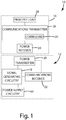
- the wireless power transfer system 10 generally includes a wireless power supply 12 and a remote device 14.
- the wireless power supply 12 is capable of wirelessly supplying power to the remote device 14 by an inductive field that can be coupled to the remote device 14.
- the remote device 14 is configured to send communications to the wireless power supply 12 by overlaying the communications onto the inductive field produced by the wireless power supply 12.
- the wireless power supply 12 generally includes power supply circuitry 16, signal generating circuitry 18, a power transmitter 20 and a wireless communication receiver 22.
- the wireless communication receiver 22 is configured to receive communication from the remote device 14 via backscatter modulation.
- the remote device 14 generally includes a power receiver 24, a communications transmitter 26 and a principle load 28.
- the communication transmitter 26 may include a communication load 30 that can be selectively applied to vary the impedance of the remote device 14 and thereby create data signals that are reflected back to the wireless power supply 12 through reflected impedance.
- the communication transmitter 26 is configured to produce signals by modulating a load a plurality of times during each bit time.
- the characteristics of each modulation may be independent of the frequency of the carrier signal and may remain essentially constant regardless of changes in the frequency of the carrier signal. However, the number of modulations occurring during a bit time may be a function of the frequency of the carrier signal, for example, a fraction or a multiple of the carrier signal frequency.
- the load may be modulated to provide an improved form of phase keyed shifting or an improved form of frequency keyed shifting.
- the communication signals may be decoded by sensing a characteristic of power affected by the modulations and averaging the sensed characteristic over time.
- the present invention relates to systems and methods for transmitting communications in the context of a wireless power transfer system.
- the systems and methods of the present invention relate to the transfer of communications by overlaying data onto the electromagnetic fields used to transmit power.
- the present invention is well-suited for use in transmitting essentially any type of data.
- the communication systems and methods of the present invention may be used to transmit control signals relating to operation of the wireless power transfer system, such as signals that identify the remote device, provide wireless power supply control parameters or provide information in real-time relating to wireless power supply (e.g. current, voltage, temperature, battery condition, charging status and remote device status).
- the communication systems and methods may be used to transfer data unrelated to the wireless power transfer system, such as transferring information associated with features of the remote device, including synchronizing calendars and to-do lists or transferring files (e.g. audio, video, image, spreadsheet, database, word processing and application files-just to name a few).
- the present invention is described in the context of various embodiments in which communications are transmitted from the remote device 14 to the wireless power supply 12. Although not described in detail, it should be understood that the present invention may also be used to transfer communications from the wireless power supply 12 to the remote device 14 (or to a plurality of remote devices).
- the present invention is described in connection with an adaptive wireless power supply 12 that is capable of adjusting operating parameters, such as operating frequency, resonant frequency, rail voltage and/or duty cycle, based on communications (e.g. data) from the remote device 14.
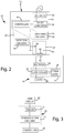
- the wireless power supply 12 of Fig. 1 generally includes power supply circuitry 16, signal generating circuitry 18, a power transmitter 20 and a communications receiver 22.
- Fig. 2 provides a more detailed schematic of one embodiment of the wireless power supply 12 of Fig. 1 .
- the power supply circuitry 16 generally includes a rectifier 32 and a DC-DC converter 34.
- the rectifier 32 and DC-DC converter 34 provide the appropriate DC power for the power supply signal.
- the power supply circuitry 16 may alternatively be essentially any circuitry capable of transforming input power to the form used by the signal generating circuitry 18.
- the signal generating circuitry 18 includes a portion of controller 36 and switching circuitry 38.
- the controller 36 is configured, among other things, to operate the switching circuitry 38 to apply the desired power supply signal to the power transmitter 20.
- the power transmitter 20 includes a tank circuit 40 having a primary coil 42 and a ballast capacitor 44.
- the communication receiver 22 includes a detector circuit 46 and portions of controller 36. The detector circuit 46 is coupled to the tank circuit 40 in this embodiment, but may be coupled elsewhere as described in more detail below.
- the wireless power supply 12 of this embodiment includes a controller 36 that performs various functions, such as controlling the timing of the switching circuit 38 and cooperating with the detector circuit 46 to extract and interpret communications signals. These functions may alternatively be handled by separate controllers or other dedicated circuitry.
- the detector circuit described generally above may be implemented in a wide variety of different embodiments.
- the detector circuit may vary from embodiment to embodiment depending upon the type of modulation/demodulation implemented in that embodiment and/or depending on the details of the power supply circuitry.
- each modulation/demodulation scheme may be implemented using a variety of different circuits.
- the detector circuit is configured to produce an output signal as a function of a characteristic of power in the power supply that is affected by data communicated through reflected impedance.
- the detector circuit 46 may include a sensor 45 to sense the current in the tank circuit 40 and demodulation circuitry 47 to convert the sensed current into a stream of high and low signals in accordance with an embodiment of the present invention.
- the detector circuit 46 may alternatively be connected to other points in the power supply 12 where power is affected by reflected impedance from the remote device 14.
- the demodulation circuitry 47 may include filtering and conditioning circuitry (not shown in Fig. 3 ) to filter and condition the output of the sensor.
- the demodulation circuitry 47 may include band pass filtering circuitry that functions primarily to attenuate high frequency oscillations that are above the frequency range of the data communications and/or to attenuate low frequency oscillations that are below the frequency range of the data communications, including without limitation any DC component in the signal.
- the signal may be passed from filtering and conditioning circuitry to a comparator (not shown in Fig. 3 ) that converts the signals to a stream of high and low signals.
- the stream of high and low signals can be provided to a controller, such as controller 36, which interprets the high and low signals as a binary data stream in accordance with an embodiment of the present invention.
- controller 36 interprets the high and low signals as a binary data stream in accordance with an embodiment of the present invention.
- the remote electronic device 14 uses a bi-phase encoding scheme to encode data.
- a binary 1 is represented in the encoded data using two transitions with the first transition coinciding with the rising edge of the clock signal and the second transition coinciding with the falling edge of the clock signal.
- a binary 0 is represented by a single transition coinciding with the rising edge of the clock signal.
- the controller is configured to decode the comparator output using a corresponding scheme.
- the present invention provides a variety of alternative methods for modulating the biphase encoded data onto a power signal and for demodulating communications extracted from the power signal.
- the remote device 14 may include a generally conventional electronic device, such as a cell phone, a media player, a handheld radio, a camera, a flashlight or essentially any other portable electronic device.
- the remote device 14 may include an electrical energy storage device, such as a battery, capacitor or a super capacitor, or it may operate without an electrical energy storage device.
- the components associated with the principle operation of the remote device 14 are generally conventional and therefore will not be described in detail. Instead, the components associated with the principle operation of the remote device 14 are generally referred to as principle load 28. For example, in the context of a cell phone, no effort is made to describe the electronic components associated with the cell phone itself.
- the remote device 14 generally includes a secondary coil 52, a rectifier 54, a communications transmitter 26 and a principle load 28.
- the secondary coil 52 may be a coil of wire or essentially any other inductor capable of generating electrical power in response to the varying electromagnetic field generated by the wireless power supply 12.
- the rectifier 54 converts the AC power into DC power.
- the device 14 may also include a DC-DC converter in those embodiments where conversion is desired. In applications where AC power is desired in the remote device, the rectifier 54 may not be necessary.
- the communications transmitter 26 of this embodiment includes a controller 56 and a communication load 30. In addition to its role in communications, the controller 56 may be configured to perform a variety of functions, such as applying the rectified power to the principle load 28.
- the principle load 28 may include a power management block capable of managing the supply of power to the electronics of the remote device 14.
- a conventional electronic device may include an internal battery or other electrical energy storage device (such as a capacitor or super capacitor).
- the power management block may determine when to use the rectified power to charge the device's internal battery and when to use the power to power the device. It may also be capable of apportioning the power between battery charging and directly powering the device.
- the principle load 28 may not include a power management block.
- the controller 56 may be programmed to handle the power management functions or the electronic device 14 may include a separate controller for handling power management functions.
- the controller 56 includes programming that enables the controller 56 to selectively apply the communication load 30 to create data communications on the power signal using a backscatter modulation scheme.
- the controller 56 may be configured to selectively couple the communication load 30 to the secondary coil 52 at the appropriate timing to create the desired data transmissions.
- the communication load 30 may be a resistor or other circuit component capable of selectively varying the overall impedance of the remote device 14.
- the communication load 30 may be a capacitor or an inductor (not shown).
- the illustrated embodiments show a single communication load 30, multiple communication loads may be used.
- the system may incorporate a dynamic-load communication system in accordance with an embodiment of U.S. Application Serial No.
- the communications load 30 may be a dedicated circuit component (e.g. a dedicated resistor, inductor or capacitor), the communication load 30 need not be a dedicated component. For example, in some applications, communications may be created by toggling the principle load 28 or some portion of the principle load 28.
- the communications load 30 may be located in essentially any position in which it is capable of producing the desired variation in the impedance of the remote device 14, such as between the secondary coil 52 and the rectifier 54.
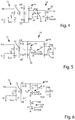
- Fig. 4 shows a circuit diagram of one embodiment of the present invention. It should be understood that the circuit diagram is a simplified diagram intended to represent the principle circuit components associated with the creation of communication signals in the remote device 14. In this embodiment, a single load is modulated to provide communications signals.
- the Fig. 4 embodiment generally includes a secondary coil 52, full bridge rectifier 54, a load 28, a bulk capacitor 60 and a communication subcircuit 62.
- the secondary coil 52 may be essentially any inductor, but is a coil of wire in the illustrated embodiment.
- the rectifier 54 is a full bridge rectifier including diodes D1-D4. Alternative rectifier configurations may be used.
- the load 28 represents the functional load of the remote device 14.
- the bulk capacitor 60 is selected to help smooth and filter power applied to load 28.
- the communication subcircuit 62 may include a load resistor 30 and a FET 64 connected in series between the load 28 and ground. Although not shown in Fig. 4 , the controller 56 is operatively coupled to the FET 64 so that the controller 56 can selectively modulate the load resistor 30 to generate communication signals.
- FIG. 5 shows an embodiment with a single communication load 30 that has an independent high side rectifier bridge 66.
- a full bridge power rectifier 54 is provided to rectify power supplied to the load 28.
- the power rectifier 54 includes diodes D1-D4.
- the communication subcircuit 62 includes a communication load 30 and a FET 64 with an independent communication bridge 66.
- the independent communication bridge includes diodes D5-D6.
- the controller 56 (not shown in Fig. 5 ) operates FET 64 to modulate the communication load 30.
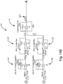
- Fig. 6 shows another alternative embodiment in which two separate communication subcircuits 62a-62b are used to apply the communication load 30a-30b.
- a full bridge rectifier 54 is provided to rectify power applied to the load 28.
- the full bridge rectifier includes diodes D1-D4.
- the first communication subcircuit 62a is connected to the common node of diodes D4-D1 to modulate the communication load during one half of the drive waveform.
- the first communication subcircuit 62a includes a communication load 30a and a FET 64a.
- the FET 64a is operatively coupled to the controller 56 (not shown in Fig. 6 ) so that the controller can selectively modulate the communication load 30a.
- the second communication subcircuit 62b is connected to the common node of diodes D3-D2 to modulate the communication load 30b during the other half of the drive waveform.
- the second communication subcircuit 62b is essentially identical to the first communication subcircuit 62a.
- the second communication subcircuit 62b includes a communication load 30b and a FET 64b.
- the FET 64b is operatively coupled to the controller 56 so that the controller can selectively modulate the communication load 30b.
- the present invention may also be used to modulate a load to apply communication signals to a split secondary coil (e.g. a center-tapped coil).
- a split secondary coil e.g. a center-tapped coil
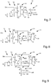
- Figs. 7-9 show various alternative remote device circuits.
- Fig. 7 shows a circuit with a single communication subcircuit and a shared full-wave rectifier.
- the secondary coil 52 is a center-tapped, split coil.
- the communication subcircuit 62 includes a communication load 30 and a FET 64.
- the FET 64 is operatively coupled to the controller 56 (not shown in Fig. 7 ) so that the controller 56 can selectively modulate the communication load 30.
- Fig. 8 is an alternative embodiment with a center-tapped secondary 52 and an independent communication bridge 66.
- the power rectifier 54 includes diodes D1-D2.
- the communication subcircuit 62 is coupled to both sides of the secondary by separate diodes D3-D4.
- the communication subcircuit 62 includes a communication load 30 and a FET 64 for selectively coupling the communication load 30 to ground.
- the FET 64 is operatively coupled to controller 56 so that the controller 56 can selectively modulate the communication load 30.
- Fig. 9 is yet another alternative embodiment.
- This embodiment includes a split secondary 52, a full-wave power rectifier 54, and two communication bridges 66a-66b with independent communication control.
- the power rectifier 54 includes diodes D1-D2 arranged between the split secondary 52 and the load 28.
- the first communication bridge 66a is connected to the node connecting the first side of the secondary 52 and diode D1 to modulate the communication load during one half of the drive waveform.
- the first communication bridge 66a includes diode D3 and a first communication subcircuit 62a.
- the first communication subcircuit 62a includes a communication load 30a and a FET 64a.
- the FET 64a is operatively coupled to the controller 56 (not shown in Fig.
- the second communication bridge 66b is connected to the node connecting the opposite side of the secondary 52 and diode D2 to modulate the communication load 30b during the other half of the drive waveform.
- the second communication bridge 66b includes diode D4 and a second communication subcircuit 62b.
- the second communication subcircuit 62b is essentially identical to the first communication subcircuit 62a.
- the second communication subcircuit 62b includes a communication load 30b and a FET 64b.
- the FET 64b is operatively coupled to the controller 56 so that the controller can selectively modulation the communication load 30b.
- the remote device 14 of Fig. 2 is described with a single controller that handles all of the control functions of the wireless power-related components, these functions may be divided across multiple controllers. For example, there may be a separate controller to handle communications. In applications with separate communication subcircuits, the remote device 14 may include separate controllers for operating the separate communication subcircuits.
- the present invention provides a variety of alternative communication methods that may provide improved performance in the context of wireless power transfer systems. These methods may be implemented using the wireless power transfer systems described above or any alternative systems capable of carrying out the methods of the present invention.
- the communication methods of the present invention will be described primarily in the context of a wireless power transfer system incorporating the simplified circuit diagram of Fig. 4 .
- the following paragraphs describe alternative communications methods with reference to various waveform diagrams. These waveform diagrams include a first figure showing the data (i.e. the desired stream of ones and zeros), a second figure showing the data stream encoded using biphase modulation, and then a series of figures that show further details during a short period of time containing a transition from a logic low to a logic high.
- the communications methods of the present invention are described in connection with a carrier waveform operating at 100kHz, but the frequency may vary.
- the various communications methods are described in connection with a carrier waveform operating a single frequency (.e.g. 100kHz), it should be understood that the frequency of the carrier waveform may vary over time and that the communications methods of the present invention will automatically adapt to frequency changes.
- the carrier waveform frequency may vary over time between 50kHz and 200kHz.
- the various communication methods are described in connection with data encoded at a fixed frequency of 2kHz. This fixed frequency is merely exemplary and the data encoding frequency may vary from application to application.
- the communications are encoded by modulating a communication load at a rate that is a fraction of the drive frequency, such as an even-integer fraction.
- the communication resistor is modulated at one half the frequency of the carrier waveform.
- the modulation signal is created by combining the modulation clock and the encoded data. More specifically, in this embodiment, the modulation clock waveform is XORed with the encoded data waveform to produce the modulation signal.
- the modulation signal is created by combining the modulation clock and the encoded data.
- Figs. 10C-10H show a short segment of the data stream during which there is a transition from a low signal to a high signal.
- Fig. 10C shows the carrier waveform, which as noted above is about 100kHz for this illustration.
- Fig. 10D shows the modulation clock signal.
- the frequency of the modulation clock signal is one-half the frequency of the carrier (or about 50kHz) in this illustration.
- the data stream is shown in Fig. 10E .
- the data signal ( Fig. 10D ) is XOR with the encoded data signal ( Fig. 10E ) to produce the XOR waveform shown in Fig. 10F .
- the modulation clock waveform is copied when the encoded data is low and is inverted when the encoded data is high.
- the modulated signal is applied to the carrier waveform, the resulting modulated carrier waveform is shown in Fig. 10G .
- Alternate time slicing of the resulting modulated carrier waveform is shown in Fig. 10H .
- the communication signal may be received, demodulated and decoded using a variety of alternative systems and methods.
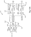
- the present invention will be described in connection with communication receiver 22 of Fig. 3 and the demodulation circuitry of Fig. 11 .
- the current sensor 45 produces a signal that is representative of the current in the tank circuit 40 (see Fig. 3 ).
- the current sensor 45 may be a current sense transformer that produces a signal having a voltage that varies in proportion with the magnitude of the current in the tank circuit 40.
- the current sensor 45 may be an output taken from a divider having a scaling resistor and capacitor as shown in Figs. 4-9 .
- the current sensor 45 may be replaced by essentially any detector or similar circuit component capable of producing a signal that is representative of a characteristic of power in the power supply 12 that is affected by the reflected impedance of the remote device 14.
- the detector circuit 46 includes a pair of amplifiers 102a-102b that produce a buffer copy and an inverted buffer copy of the signal output by the current sensor (see Fig. 11 ).
- the current sensor signal may be passed to both an amplifier and an inverting amplifier arranged in parallel with respect to one another.
- the output of the amplifier and the inverting amplifier may be passed to a pair of multiplexors 104a-104b that are coupled to a time slicing clock that is synchronized with the modulation clock in the remote device 14.
- the time slicing clock controls whether the buffer copy or the inverted copy of the current signal is passed to the remainder of the detector circuitry.
- the clock signal is synchronized to the drive frequency divided by two.
- the two multiplexors 104a-104b include opposite NO/NC inputs to provide a differential signal.
- the multiplexor clocking may be inverted to provide a differential signal.
- the multiplexors of the illustrated embodiment have two inputs, the multiplexors 104a-104b could alternatively have a single input and the output may be left floating on the alternate clock phase. This could reduce the signal strength of the amplifier chain.
- the clock signal may be derived from a variety of sources, such as the drive signal, the primary coil voltage, the primary coil current or a 90 degree shifted version of any of the foregoing.
- multiplexor 104a passes the buffer copy during the "A" time slices and passes the inverted copy during the "B” time slices
- multiplexor 104b passes the buffer copy during the "B” time slices and passes the inverted copy during the "A" time slices.
- each multiplexor 104a-104b is passed through a separate amplifier chain.
- the output of each multiplexor 104a-104b is passed to separate averaging circuitry 106a-106b.
- Each of these averaging circuits 106a-106b outputs the average of the minimum and maximum of its respective input, which may provide improved performance over a straight average in some applications because it may be less influenced by the shape of the waveform and more sensitive to extreme values. Although potentially beneficial in some applications, the outputs need not be averages of the minimum and maximum.
- the averaging circuits 106a-106b may alternatively output a straight average of their respective input signals.
- the outputs of the averaging circuits 106a-106b are passed to separate low pass filters 108a-108b.
- the filters 108a-108b may be two pole 5kHz low pass filters. These low pass filters 108a-108b function primarily to remove the AC components of the signal above the communication frequency range. Although this function is performed in the illustrated embodiment with op-amps, the op-amps may be replaced by alternative filtering circuitry, such as a passive filter or a digital filter.
- the outputs of the low pass filters 108a-108b are passed to separate amplifiers 110a-110b.
- the amplifiers 110a-110b are AC coupled amplifiers that amplify the filtered signal, maintaining a center point around Vbias. In this embodiment, the AC coupling removes any DC offset and serves as a single pole high pass filter.
- the outputs of the amplifiers 110a-110b are passed to separate low pass filters 112a-112b. These low pass filters 112a-112b remove AC components of the signal above the communication frequency range and help to remove noise imparted by the AC amplifier 110a-110b. Although low pass filters 112a-112b are implemented in the illustrated embodiment with op-amps, the op-amps may be replaced by alternative filtering circuitry, such as a passive filter or a digital filter. In some applications, the signal-to-noise ratio of the outputs of the amplifiers may be sufficient so that low pass filters 112a-112b are unnecessary.
- the outputs of the final low pass filters 112a-112b are separately passed to a comparator 114.
- the comparator 114 combines the differential signals from the two amplifier chains back into a single, "digitized" signal that can be readily decoded by a microcontroller, such as controller 36.
- a microcontroller such as controller 36.
- the detector circuit 46 may alternatively incorporate a single ended detection chain.
- the detector circuit may include only the topmost chain of Fig. 11 .
- the dual-chain circuitry of Fig. 11 may provide improved performance in some applications because the differential pair of amplifier chains provides improved signal-to-noise ratio as one signal is increasing in voltage while the other is decreasing. As a result, DC drift is unlikely to distort the signal.
- the comparator of this alternative embodiment is configured to provide a high or low output based on a comparison of the amplitude of the input signal with a reference signal.
- the comparator may include a first input that receives the signal from the single detection chain and a second input that is coupled to a reference signal, Vbias.
- the reference signal may be set to be slightly lower than the DC component of the amplified signal. Accordingly, the comparator output will remain high when no communication is present in the signal. If communication is present, then the comparator output toggles between high and low in correspondence with the communication signals.
- the output of the comparator 114 is passed to the controller 36 for decoding. In this case, decoding is achieved using a biphase decoding scheme.
- communications are encoded by modulating a communication load at a rate that is a fraction of the drive frequency, similar to the embodiment described above with respect to Figs. 10A-G and 11 , with some exceptions.
- the communication load in this embodiment is modulated during a fraction of the drive waveform, such as one-half the drive waveform.
- a communication load is modulated at one-half the frequency of the carrier waveform.
- the modulation clock waveform may be XORed with the encoded data waveform to produce a modulator control waveform.
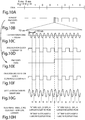
- Figs. 16C-H show a short segment of the data stream during which there is a transition from a low signal to a high signal.
- Fig. 16C shows the carrier waveform, which as noted above is about 100 kHz for this illustration.
- Fig. 16D shows the modulation clock waveform having a frequency that is one-half the frequency of the carrier (or about 50 kHz) in this illustration.
- the data stream is shown in Fig.
- the communication load may be modulated according to the XORed waveform for a full cycle of the carrier waveform, or in other words, at a 50% duty cycle using a modulated clock waveform having a frequency that is one-half the carrier frequency.
- the XORed waveform is applied for approximately one-half the cycle of the carrier waveform, or in other words, at a 25% duty cycle using a modulated clock waveform having a frequency that is one-half the carrier frequency.
- the communication load may be applied for less time than in the previous embodiment, and to increase the magnitude of either a peak or a tough-but not both-of every other waveform of the carrier waveform in order to communicate the data.
- This 25% duty cycle modulation may be achieved by generating an XOR waveform similar to the XOR waveform illustrated in the embodiments of Figs. 10A-G ; but rather than applying the XOR waveform during a full cycle of the carrier waveform, the XOR waveform may be applied during one-half of each cycle of the carrier waveform.
- applying the XOR waveform for one-half of each cycle of the carrier waveform may be accomplished by selectively modulating one of the communication loads 30a-30b-not both-or put differently, modulating one leg of the secondary coil 52 instead of both legs.
- this embodiment implements a 25% duty cycle using an XOR waveform similar to that of the embodiments above, the 25% duty cycle may be achieved instead by modifying the modulation clock waveform to have a 25% duty cycle and XORing it with the encoded data waveform.
- the communication load 30 may be modulated according to this XORed waveform in order to apply the communication load 30 for approximately one-half of each cycle of the carrier waveform.
- Propagation delays inherent to the electronics of this embodiment, and other embodiments, may cause the modulation clock to be delayed with respect to the carrier waveform.
- this propagation delay can be seen by the slight shift in the modulation clock waveform with respect to the zero crossing of the carrier waveform.
- this propagation delay may affect when the communication load is applied relative to the carrier waveform, and whether the remote device 14 attempts to adapt or compensate for the delay.
- the propagation delay may affect the choice of which leg of the secondary coil 52 to modulate in order to implement 25% duty cycle modulation.
- the current through the load resistor 30a (coupled to the first leg of the secondary coil 52) during modulation cycles is shown in Fig. 16H
- the current through the load resistor 30b (coupled to the second leg of the secondary coil 52) during modulation cycles is shown in Fig. 16G . Because the modulation clock waveform of Fig.
- a propagation delay prevents full modulation of the load resistor 30a as illustrated by the chopped modulator current in Fig. 16H .
- a communication load may be modulated on a leg of the secondary that is opposite the leg which generates the modulation clock waveform. For example, in the illustrated embodiment of Fig. 16G , full modulation is achieved at 25% duty cycle by modulating the load resistor 30b coupled to the second leg of the secondary coil 52.
- the communication load of this embodiment may be one or more impedance elements, such as a load resistor or one or more alternative components.
- the communication load may be resistive, capacitive, or inductive, or a combination thereof.
- Figs. 4-9 show a load resistor 30, this embodiment may in some cases function better with a load capacitor in place of the load resistor 30.
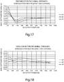
- Figs. 17 and 18 illustrate potential differences between embodiments of Figs. 16A-H that modulate at 25% duty cycle using a single load resistor 30a and a 50% duty cycle modulator.
- Fig. 17 shows communication nulls or inversion that may result from depleting the energy in the coils for two consecutive cycles with embodiments using a 50% duty cycle modulator. Specifically, at output powers of approximately 15-30W, the modulation depth may invert or go below 0.0 mV, causing a null communication zone.
- the present invention may provide communication circuitry that avoids communication inversion. Further potential attributes of the 25% duty cycle embodiments may be a reduction or elimination of audible noise during communication, though 50% duty cycle embodiments may also reduce or eliminate audible noise.
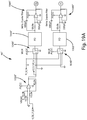
- the communication signal may be received, demodulated, and decoded using systems and methods similar to the embodiments described above with respect to Fig. 11 , with some exceptions.
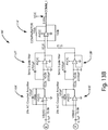
- this embodiment uses peak detector circuitry 106a-b" and 106a-b"' and includes two detector circuits 46" and 46"' to demodulate the communication signal. Otherwise, this embodiment and its alternatives are similar to other embodiments described herein.
- the communication load may be applied during one-half of the carrier wave cycle.
- the modulation may cause a level shift to be reflected through the inductive coupling to the wireless power supply that generally affects either the peaks or the troughs-but not both-of the current sensed by the current sensor.
- (a) levels of the peak current or voltage through the primary coil from even to odd cycles may shift, or (b) levels of the trough current or voltage through the primary coil from even to odd cycles may shift. If the dot orientation (e.g.
- this embodiment utilizes two detector circuits 46" and 46'" to sense level shifts in either the peaks or the troughs due to communication load modulation.
- the respective outputs (A and B) of the two detector circuits 46" and 46"' are then combined, such as being ORed together, to yield a digital representation of the communication signal modulated through the inductive coupling.
- a single detector circuit may be used to detect level shifts in either the peaks or the troughs, whichever is expected, depending on the known dot convention and which leg of the secondary 52 is being modulated. It should be appreciated that knowing the dot orientation may be unnecessary in embodiments that use 50% duty cycle modulation because level shifts due to modulation of the communication load occur in both the peaks and the troughs.
- the first and second detector circuits 46" and 46'" are now described in further detail.
- the first detector circuit 46" produces a buffer copy of the signal output by the current sensor
- a second detector circuit 46'" produces an inverted buffer copy of the signal output by the current sensor.
- the first detector circuit 46" samples and time slices peaks of the carrier wave to detect a level shift in response to application of a communication load
- the second detector circuit 46'" samples and time slices the troughs of the carrier wave to detect a level shift in response to application of a communication load.
- the multiplexor 104a" of detector 46" passes a buffered copy during "A" time slices
- the multiplexor 104b" of detector 46" passes a buffered copy during "B” time slices.
- the "A" time slices and the "B" time slices are passed through a separate amplifier chain, which with some exceptions may be similar to the amplifier chain of the illustrated embodiment of Fig. 11 .
- the outputs of the multiplexors 104a-b" are passed to separate peak detectors 106a-b". Each of the peak detectors 106a-b" outputs the peak value of its respective input during a time slice.
- This peak detection may provide improved signal detection by capturing level shifts resulting from modulation of the communication load.
- the peak detector may also cancel out any asymmetry imposed by half-bridge driver hardware of the wireless power supply.
- the peak detector 106a-b" is used in the illustrated embodiment of Fig. 19 , but the peak detector may also be implemented in other embodiments described herein.
- the peak detector may be replaced by a trough detector, which may detect minimum conditions rather than maximum conditions in the signal.
- the outputs of the peak detectors 106a-b" are each passed through separate amplifier chains as discussed above, and eventually compared against each other using a differential amplifier, such as comparator 114". If a level shift is detected between the peaks of the buffered, non-inverted signal in the "A" time slices as compared to the "B" time slices, the comparator 114" outputs a "digitized” signal that can be readily decoded by a microcontroller, such as controller 36. As an example, if the peak value of the signal during the "A" time slices is higher than the peak value of the signal during the "B” time slices, a logic high will be output from the detector 46". Conversely, if the peak value of the signal during "A" time slices is lower than the peak value of the signal during the "B” time slices, then a logic low will be output from the detector 46".
- the detector 46'" detects the opposite of detector 46"; rather than detecting peaks in the signal, detector 46'" detects troughs or minimums in the signal. For example, by detecting a level shift in the troughs, detector 46'" may demodulate data encoded within the signal.
- the multiplexor 104a'" of detector 46'" passes a buffered inverted copy of the signal during "A" time slices
- the multiplexor 104b"' passes a buffered inverted copy of the signal during "B” time slices.
- the "A" time slices and the "B" time slices are passed through a separate amplifier chain, which with some exceptions is similar to the amplifier chain of the illustrated embodiment of Fig. 11 .
- the outputs of the multiplexors 104a-b"' are passed to separate peak detectors 106a-b"', which in detector 46'" detect troughs or minimums in the signal.
- Each of the peak detectors 106a-b"' outputs the peak value of the inverted signal (the trough of the non-inverted signal) of its respective input during a time slice.
- the outputs of the peak detectors 106a-b"' are each passed through separate amplifier chains, and eventually compared against each other using a differential amplifier, such as comparator 114"'. As before, if a level shift is detected between the troughs of the buffered, non-inverted signal in the "A" time slices as compared to the "B" time slices, the comparator 114"' outputs a "digitized” signal that can be readily decoded by a microcontroller.
- results may differ depending on the manner of modulating the communication load.
- detector 46" would not detect a level shift between peak values of the buffered, non-inverted signal during the "A" time slices and the "B" time slices.
- the communication load is being modulated during the trough cycle of the carrier wave, not the peak cycle, and therefore the peaks of the signal are generally unaffected by modulation of the communication load.
- Detector 46"' would detect a level shift between the peak values of the buffered, inverted signal during the "A" time slices and the "B” time slices. Because the communication load is being modulated during the trough cycle of the carrier wave, the peaks of the inverted form of the signal (troughs of the non-inverted signal), as measured by peak detectors 106a-b'" would identify a level shift between the "A" time slices and the "B" time slices, and output the level shift as a "digitized” signal to be decoded by a microcontroller as described previously.
- communications are encoded by modulating a communication load at a rate that is a multiple of the drive frequency, such as an even-integer multiple.
- the communication resistor is modulated at four times the frequency of the carrier waveform.
- This embodiment may include a phase lock loop ("PLL") to generate a modulation clock waveform that remains in phase with the carrier waveform.
- Fig. 12A shows a sample data stream of Is and 0s.
- Fig. 12B shows the sample data stream encoded using a biphase encoding stream.
- the modulation signal is created by combining the modulation clock and the encoded data using different functions for the positive and negative halves of each cycle of the waveform.
- the modulation clock waveform is XORed with the encoded data waveform, and during the negative half of the carrier waveform, the modulation clock waveform is XOR#ed with the encoded data waveform.
- Fig. 12C shows the carrier waveform, which as noted above is about 100kHz.
- Fig. 12D shows the modulation clock signal.
- the frequency of the modulation clock signal is four times the frequency of the carrier or about 400kHz in this illustration.
- the data stream is shown in Fig. 12E . As noted above, this illustration shows a short portion of the data stream including a single transition for low to high.
- the XOR waveform is shown in Fig. 12F and the XOR# waveform is shown in Fig. 12G .
- the composite waveform resulting from alternately XORing or XOR#ing the data signal with the modulation clock signal provides the modulated signal as shown in Fig. 12H .
- the modulated signal is applied to the carrier waveform, the resulting modulated carrier waveform is shown in Fig. 12I .
- Fig. 12I represents an idealized waveform. In practice, the modulated signal is unlikely to produce instantaneous variations in the primary current. Instead, the current is likely to take some time to transition and the actual waveform is likely to have transition regions rather than clean jumps between time slices.
- the communication signal produced by this second communications method may be received and decoded using a variety of alternative systems and methods.
- the present invention will be described in connection with communication receiver 22 of Fig. 2 and the demodulation circuitry of Fig. 13 .
- the demodulation circuitry of Fig. 13 is similar to the demodulation circuitry of Fig. 11 . It does not, however, include averaging circuitry 106a-106b.
- the current sensor 45 produces a signal that is representative of the current in the tank circuit.
- the current sensor 45 may be a current sense transformer that produces a signal having a voltage that varies in proportion with the magnitude of the current in the tank circuit 40.
- the current sensor 45 may be an output taken from a divider having a scaling resistor and capacitor as shown in Figs. 4-9 .
- the current sensor 45 may be replaced by essentially any detector capable of producing a signal that is representative of a characteristic of power in the power supply 12 that is affected by the reflected impedance of the remote device 14.
- the detector circuit 46' includes a pair of amplifiers 102a'-102b' that produce a buffer copy and an inverted buffer copy of the signal output by the current sensor.
- the current sensor signal may be passed to an amplifier and an inverting amplifier arranged in parallel with respect to one another.
- the output of the amplifier and the inverting amplifier may be passed to a pair of multiplexors 104a'-104b' that are coupled to a time slicing clock that is synchronized with the modulation clock in the remote device 14.
- the time slicing clock controls whether the buffer copy or the inverted copy of the current signal is passed to the remainder of the detector circuitry.
- the clock signal is synchronized to the drive frequency multiplied by four.
- the two multiplexors 104a'-104b' include opposite NO/NC inputs to provide a differential signal.
- the clocking of one multiplexor with respect to another may be inverted to provide a differential signal.
- multiplexor 104b' clocking may be inverted with respect to multiplexor 104a' clocking in order to provide a differential signal.
- the multiplexors of the illustrated embodiment have two inputs, the multiplexors 104a'-104b' could alternatively have a single input and the output may be left floating on the alternate clock phase. This could reduce the signal strength of the amplifier chain.
- the clock signal may be derived from a variety of sources, such as the drive signal, the primary coil voltage, the primary coil current or a 90 degree shifted version of any of the foregoing.
- multiplexor 104a' passes the buffer copy during the "A" time slices and passes the inverted copy during the "B” time slices
- multiplexor 104b' passes the buffer copy during the "B” time slices and passes the inverted copy during the "A" time slices.
- each multiplexor 104a'-104b' is passed through a separate amplifier chain.
- the output of each multiplexor 104a'-104b' is passed to a separate low pass filter 108a'-108b'.
- the filters 108a'-108b' may be two pole 5kHz low pass filters. These low pass filters 108a'-108b' function primarily to remove the AC components of the signal above the communication frequency range. Although this function is performed in the illustrated embodiment with op-amps, the op-amps may be replaced by alternative filtering circuitry, such as a passive filter or a digital filter.
- the outputs of the low pass filters 108a'-108b' are passed to separate amplifiers 110a'-110b'.
- the amplifiers 110a'-110b' are AC coupled amplifiers that amplify the filtered signal, maintaining a center point around Vbias. In this embodiment, the AC coupling removes any DC offset and serves as a single pole high pass filter.
- the outputs of the amplifiers 110a'-110b' are passed to separate low pass filters 112a'-112b'. These low pass filters 112a'-112b' remove AC components of the signal above the communication frequency range and help to remove noise imparted by the AC amplifier 110a'-110b'.
- low pass filters 112a'-112b' are implemented in the illustrated embodiment with op-amps, the op-amps may be replaced by alternative filtering circuitry, such as a passive filter or a digital filter. In some applications, the signal-to-noise ratio of the outputs of the amplifiers may be sufficient so that low pass filters 112a'-112b' are unnecessary.
- the outputs of the final low pass filters 112a'-112b' are separately passed to a comparator 114'.
- the comparator 114' combines the differential signals from the two amplifier chains back into a single, "digitized" signal that can be readily decoded by a microcontroller, such as controller 36.
- the composite waveform combines to provide a negative DC offset when the encoded data is low, and to provide a positive DC offset when the encoded data is high.
- the output of the comparator 114' may be passed to the communication controller 36 for decoding. In this case, the communication controller 36 will decode the binary stream using the same scheme used to encode the data in the remote device 14, which in this illustration is a biphase encoding scheme.
- the detector circuit 46' may alternatively incorporate a single ended detection chain.
- the detector circuit may include only the topmost chain of Fig. 13 , and the comparator 114' may have its negative input referenced to Vbias.
- the dual-chain circuitry of Fig. 13 may provide improved performance in some applications because the differential pair of amplifier chains provides improved signal-to-noise ratio as one signal is increasing in voltage while the other is decreasing. As a result, DC drift is unlikely to distort the signal.
- the communications are encoded by modulating a communication load at one of two different frequencies.
- the two different frequencies may be fixed frequencies. Having two different fixed frequencies for modulation may simplify the filter design for demodulation in the wireless power supply.
- the two different frequencies may be fractions or multiples of the drive frequency, such as an integer fraction or an integer multiple.
- the communication resistor is modulated at one frequency to represent a logic high and at a different frequency to represent a logic low.
- the communications controller 36 includes two different modulation clocks-one at 1/8 th the frequency of the carrier waveform and the other at 1/10 th the frequency of the carrier waveform. The frequency of the modulation clocks may vary from application to application.
- the modulation signal is a composite of the two modulation clocks created by combining the first modulation clock during a logic low and the second modulation clock during a logic high.
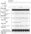
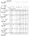
- the frequency shifting methodology of this embodiment will be described in more detail with references to Figs. 14A-14H.
- Fig. 14A shows a sample data stream of Is and 0s.
- Fig. 14B shows the sample data stream encoded using a biphase encoding scheme.
- the process for creating the modulated carrier waveform is described in more detail with reference to Figs. 14C-14H , which show a short portion of the data stream containing a transition from a low signal to a high signal.
- Fig. 14C shows the carrier waveform, which as noted above is about 100kHz for this illustration.
- FIG. 14D shows the modulation clock A signal.
- the frequency of modulation clock A is one eighth the frequency of the carrier.
- Fig. 14E shows the modulation clock B signal.
- the frequency of modulation clock B is one tenth the frequency of the carrier.
- the data stream is shown in Fig. 14F .
- the modulated carrier waveform is created by combining the carrier waveform ( Fig. 14C ) with either modulation clock A signal ( Fig. 14D ) or modulation clock B signal ( Fig. 14E ) using the encoded data signal (Fig. F) as a key. More specifically, during a low data signal, the carrier waveform is combined with the modulation clock A signal and, during a high data signal, the carrier waveform is combined with the modulation clock B signal.
- the resulting modulation clock waveform is shown in Fig. 14G .
- the modulation clock waveform modulates at one frequency while the encoded data is low, and switches to modulation at the other frequency when the encoded data is high.
- the waveform modulates more quickly for a logic low than for a logic high.
- each modulation includes four cycles of the carrier waveform during a logic low and five cycles of the carrier waveform during a logic high.
- the frequencies of the carrier waveform and the two modulation clock signals can be varied to alter the characteristics of the modulated carrier waveform.
- the current sensor 45 produces a signal that is representative of the current in the tank circuit.
- the current sensor 45 may be a current sense transformer that produces a signal having a voltage that varies with the magnitude of the current in the tank circuit 40.
- the current sensor 45 may be an output taken from a divider having a scaling resistor and capacitor as shown in Figs. 4-9 .
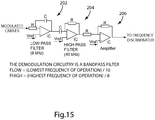
- the signal from the current sensor 45 may be passed through filtering and conditioning circuitry, such as a bandpass filter and an amplifier.
- the bandpass filter may include a low pass filter 202 and a high pass filter 204.
- the filters may be configured to filter out signals below the lowest frequency of operation divided by ten and above the highest frequency of operation divided by eight.
- the amplifier 206 may be configured to amplify the signal to an appropriate level for the frequency discriminator (not shown).
- the amplified output may be passed to the frequency discriminator (not shown).
- the frequency discriminator is an integrated circuit system (ICS) that converts frequency to a voltage.
- the output of the ICS may be provided to controller 36 for decoding.
- the frequency discriminator may include a comparator (not shown) and a controller, such as controller 36. The comparator may produce a square wave output and the controller 36 may count the edges to determine the modulation frequency.
- the communication controller 36 will decode the binary stream of logic highs and logic lows using a biphase decoding scheme.
- the filtering, conditioning and/or comparator functions may alternatively be carried out using a digital signal processor (DSP).
- DSP digital signal processor
- the output of current sense transformer (or other detector) may be fed into a DSP (not shown).
- the DSP may convert the analog signal into a digital signal and then processes the digital signal to generate high and low outputs that are consistent with the high and low outputs that would have been generated using the circuitry described above.
- the DSP may process the input signal to remove signal components occurring outside the frequency range used for communications, analyze the remaining signal to identify the communication signals then provide an output signal that drives high and low with the communication signals.
- the communication receiver includes a detector circuit that demodulates communications through a current sense transformer that provides an output representative of the current in the tank circuit.
- the communication receiver may operate using alternative methods and apparatus.
- the power supply may include a detector circuit that provides a signal indicative of the current in the input to the switching circuit (e.g. an amplifier coupled to the input of the switching circuit).
- the power supply may include a detector circuit that detects communications using the phase relationship of the voltage of the input to the switching circuit and the current in the tank circuit.
- the power supply may include a detector circuit that detects communication using the voltage in the tank circuit. Operation of some of these alternative systems and methods for detecting communications is described in more detail in U.S. Provisional Application No. 61/298021 , entitled SYSTEMS AND METHODS FOR DETECTING DATA COMMUNICATION OVER A WIRELESS POWER LINK and filed on January 25, 2010, which is published as US 2011/0204711 A1 .
Landscapes
- Engineering & Computer Science (AREA)
- Computer Networks & Wireless Communication (AREA)
- Signal Processing (AREA)
- Power Engineering (AREA)
- Near-Field Transmission Systems (AREA)
- Transmitters (AREA)
- Selective Calling Equipment (AREA)
Claims (6)
- Procédé de communication de données entre un dispositif distant (14) et une alimentation en puissance inductive à l'aide d'une modulation à clé, ledit procédé consistant:à recevoir une puissance inductive par l'intermédiaire d'un signal de transmission de puissance à fréquence variable provenant de la puissance inductive;à coder un flux de données des bits en un signal de communication;et à générer un signal de modulation à base du signal de communication et d'un signal d'horloge de modulation, dans lequel chaque bit du flux de données est représenté par une pluralité de modulations dans le signal de modulation;à moduler le signal de transmission de puissance à fréquence variable en fonction du signal de modulation en basculant une charge (30) d'un émetteur de communication (26); età faire varier le signal d'horloge de modulation en fonction des variations d'une fréquence du signal de transmission de puissance à fréquence variable, dans lequel le signal de transmission de puissance à fréquence variable est apte à varier en réponse à un changement d'au moins un paramètre de fonctionnement de l'alimentation en puissance inductive, dans lequel le signal d'horloge de modulation varie en fonction du changement de l'au moins un paramètre de fonctionnement de l'alimentation en puissance inductive, dans lequel le signal d'horloge de modulation est verrouillé en phase à une fréquence harmonique du signal de transmission de puissance à fréquence variable,caractérisé en ce que ladite modulation consiste:à générer un premier signal de commande de modulation formé par un OU exclusif (a) du signal d'horloge de modulation fonctionnant à la fréquence harmonique et (b) du signal de communication;à générer un second signal de commande de modulation formé en inversant l'OU exclusif (a) du signal d'horloge de modulation fonctionnant à la fréquence harmonique et (b) du signal de communication;à basculer la charge (30) en fonction du premier signal de commande de modulation pendant une moitié positive du signal de transmission de puissance à fréquence variable; età basculer la charge (30) en fonction du second signal de commande de modulation pendant une moitié négative du signal de transmission de puissance à fréquence variable.
- Dispositif distant (14) permettant de recevoir la puissance d'une alimentation en puissance inductive et de communiquer des données à l'alimentation en puissance inductive, ledit dispositif distant (14) comprenant:un récepteur de puissance (24) conçu pour recevoir un signal de transmission de puissance à fréquence variable;un dispositif de commande (56) conçu pour coder un flux de données des bits en un signal de modulation à base d'un signal d'horloge de modulation, chaque bit du flux de données étant représenté par une pluralité de modulations dans le signal de modulation,dans lequel le signal d'horloge de modulation varie en fonction des variations d'une fréquence du signal de transmission de puissance à fréquence variable,dans lequel le signal de transmission de puissance à fréquence variable est apte à varier en réponse à un changement d'au moins un paramètre de fonctionnement de l'alimentation en puissance inductive,dans lequel le signal d'horloge de modulation varie en fonction du changement de l'au moins un paramètre de fonctionnement de l'alimentation en puissance inductive; etun émetteur de communication (26) conçu pour basculer sélectivement une charge sur le signal de transmission de puissance à fréquence variable en fonction du signal de modulation,dans lequel le signal d'horloge de modulation est verrouillé en phase à une fréquence harmonique du signal de transmission de puissance à fréquence variable,caractérisé en ce que le dispositif de commande est en outre conçu:pour générer un premier signal de commande de modulation formé par un OU exclusif (a) du signal d'horloge de modulation fonctionnant à la fréquence harmonique et (b) du signal de communication;à générer un second signal de commande de modulation formé en inversant l'OU exclusif (a) du signal d'horloge de modulation fonctionnant à la fréquence harmonique et (b) du signal de communication;caractérisé en outre en ce que l'émetteur de communication est en outre conçu pour basculer la charge (30) en fonction du premier signal de commande de modulation pendant une moitié positive du signal de transmission de puissance à fréquence variable; etpour basculer la charge (30) en fonction du second signal de commande de modulation pendant une moitié négative du signal de transmission de puissance à fréquence variable.
- Dispositif distant (14) selon la revendication 2 en combinaison avec ladite alimentation en puissance inductive, dans lequel ladite alimentation en puissance inductive comprend des circuits de détection pour décoder le flux de données à partir du signal de transmission de puissance à fréquence variable.
- Système de transfert de puissance d'une alimentation en puissance inductive à un dispositif distant (14) selon la revendication 2 et de communication des données entre le dispositif distant (14) et l'alimentation en puissance inductive à l'aide d'une modulation à clé.
- Système selon la revendication 4, dans lequel ledit dispositif distant (14) comprend ledit émetteur de communication (26) de telle sorte que ledit dispositif distant (14) communique des données à l'alimentation en puissance inductive à l'aide d'une modulation à clé, et dans lequel ladite alimentation en puissance inductive comprend des circuits de détection pour décoder le flux de données à partir du signal de transmission de puissance à fréquence variable.
- Système selon la revendication 4, dans lequel ladite alimentation en puissance inductive comprend un émetteur de communication d'alimentation de telle sorte que ladite alimentation en puissance inductive communique les données au dispositif distant (14) à l'aide de ladite modulation à clé, et dans lequel ledit dispositif distant (14) comprend un circuit de détection pour décoder le flux de données à partir du signal de transmission de puissance à fréquence variable.
Applications Claiming Priority (3)
| Application Number | Priority Date | Filing Date | Title |
|---|---|---|---|
| US201161440138P | 2011-02-07 | 2011-02-07 | |
| US201161564130P | 2011-11-28 | 2011-11-28 | |
| PCT/US2012/023959 WO2012109137A2 (fr) | 2011-02-07 | 2012-02-06 | Système et procédé permettant des communications dans un système de transfert d'énergie sans fil |
Publications (2)
| Publication Number | Publication Date |
|---|---|
| EP2673889A2 EP2673889A2 (fr) | 2013-12-18 |
| EP2673889B1 true EP2673889B1 (fr) | 2020-04-15 |
Family
ID=45755527
Family Applications (1)
| Application Number | Title | Priority Date | Filing Date |
|---|---|---|---|
| EP12705547.3A Active EP2673889B1 (fr) | 2011-02-07 | 2012-02-06 | Procédé et dispositif de communication dans un système de transfert de puissance sans fil |
Country Status (8)
| Country | Link |
|---|---|
| US (3) | US8731116B2 (fr) |
| EP (1) | EP2673889B1 (fr) |
| JP (2) | JP6001563B2 (fr) |
| KR (1) | KR101965796B1 (fr) |
| CN (2) | CN105743545B (fr) |
| CA (1) | CA2825912A1 (fr) |
| TW (2) | TWI651952B (fr) |
| WO (1) | WO2012109137A2 (fr) |
Families Citing this family (98)
| Publication number | Priority date | Publication date | Assignee | Title |
|---|---|---|---|---|
| CA2718901C (fr) | 2008-03-17 | 2018-10-16 | Powermat Ltd. | Systeme de transmission inductif |
| US11979201B2 (en) | 2008-07-02 | 2024-05-07 | Powermat Technologies Ltd. | System and method for coded communication signals regulating inductive power transmissions |
| US8981598B2 (en) | 2008-07-02 | 2015-03-17 | Powermat Technologies Ltd. | Energy efficient inductive power transmission system and method |
| US10951063B2 (en) | 2011-02-01 | 2021-03-16 | Fu Da Tong Technology Co., Ltd. | Supplying-end module of induction type power supply system and signal detection method thereof |
| TWI570427B (zh) | 2015-10-28 | 2017-02-11 | 富達通科技股份有限公司 | 感應式電源供應器及其金屬異物檢測方法 |
| US10056944B2 (en) | 2011-02-01 | 2018-08-21 | Fu Da Tong Technology Co., Ltd. | Data determination method for supplying-end module of induction type power supply system and related supplying-end module |
| US10312748B2 (en) * | 2011-02-01 | 2019-06-04 | Fu Da Tong Techology Co., Ltd. | Signal analysis method and circuit |
| US11128180B2 (en) | 2011-02-01 | 2021-09-21 | Fu Da Tong Technology Co., Ltd. | Method and supplying-end module for detecting receiving-end module |
| US10673287B2 (en) | 2011-02-01 | 2020-06-02 | Fu Da Tong Technology Co., Ltd. | Method and supplying-end module for detecting receiving-end module |
| US9671444B2 (en) | 2011-02-01 | 2017-06-06 | Fu Da Tong Technology Co., Ltd. | Current signal sensing method for supplying-end module of induction type power supply system |
| US10038338B2 (en) | 2011-02-01 | 2018-07-31 | Fu Da Tong Technology Co., Ltd. | Signal modulation method and signal rectification and modulation device |
| US9628147B2 (en) | 2011-02-01 | 2017-04-18 | Fu Da Tong Technology Co., Ltd. | Method of automatically adjusting determination voltage and voltage adjusting device thereof |
| US10574095B2 (en) | 2011-02-01 | 2020-02-25 | Fu Da Tong Technology Co., Ltd. | Decoding method for signal processing circuit and signal processing circuit using the same |
| US10289142B2 (en) | 2011-02-01 | 2019-05-14 | Fu Da Tong Technology Co., Ltd. | Induction type power supply system and intruding metal detection method thereof |
| US9600021B2 (en) | 2011-02-01 | 2017-03-21 | Fu Da Tong Technology Co., Ltd. | Operating clock synchronization adjusting method for induction type power supply system |
| US10615645B2 (en) | 2011-02-01 | 2020-04-07 | Fu Da Tong Technology Co., Ltd | Power supply device of induction type power supply system and NFC device identification method of the same |
| US9831687B2 (en) | 2011-02-01 | 2017-11-28 | Fu Da Tong Technology Co., Ltd. | Supplying-end module for induction-type power supply system and signal analysis circuit therein |
| US10630113B2 (en) | 2011-02-01 | 2020-04-21 | Fu Da Tong Technology Co., Ltd | Power supply device of induction type power supply system and RF magnetic card identification method of the same |
| EP2673889B1 (fr) * | 2011-02-07 | 2020-04-15 | Philips IP Ventures B.V. | Procédé et dispositif de communication dans un système de transfert de puissance sans fil |
| US9166562B2 (en) | 2013-02-25 | 2015-10-20 | Qualcomm Incorporated | Impedance transformation network for improved driver circuit performance |
| US10381874B2 (en) * | 2011-03-25 | 2019-08-13 | Qualcomm Incorporated | Filter for improved driver circuit efficiency and method of operation |
| WO2013103943A1 (fr) | 2012-01-08 | 2013-07-11 | Access Business Group International Llc | Atténuation des interférences pour de multiples systèmes inductifs |
| EP2817863A1 (fr) * | 2012-01-08 | 2014-12-31 | Powermat Technologies Ltd. | Système et procédé pour fournir et commander un chargement électrique par induction |
| US9654184B2 (en) * | 2012-07-20 | 2017-05-16 | WIPQTUS Inc. | Transmitter to receiver communication link in a wireless power system |
| CN104584372B (zh) * | 2012-08-31 | 2017-07-04 | 西门子公司 | 用于给蓄电池无线充电的蓄电池充电系统和方法 |
| TWI473379B (zh) * | 2012-12-19 | 2015-02-11 | Metal Ind Res & Dev Ct | 電池管理系統之傳送接收器 |
| WO2014108785A1 (fr) | 2013-01-11 | 2014-07-17 | Koninklijke Philips N.V. | Transfert d'énergie inductive sans fil |
| TWI475779B (zh) * | 2013-01-28 | 2015-03-01 | Acer Inc | 無線充電方法及系統 |
| ITVI20130049A1 (it) * | 2013-02-28 | 2014-08-29 | Giovanni Luca Agostini | Sistema di rilevamento delle posizioni e delle prestazioni nello sport del golf |
| JP5879294B2 (ja) * | 2013-03-29 | 2016-03-08 | 日立オートモティブシステムズ株式会社 | 電池システム |
| CN104124779B (zh) * | 2013-04-28 | 2018-02-16 | 海尔集团技术研发中心 | 动态负载切换的控制方法及系统 |
| ES2827838T3 (es) | 2013-07-17 | 2021-05-24 | Koninklijke Philips Nv | Transferencia de potencia inductiva inalámbrica |
| US20150091523A1 (en) * | 2013-10-02 | 2015-04-02 | Mediatek Singapore Pte. Ltd. | Wireless charger system that has variable power / adaptive load modulation |
| US9735584B2 (en) * | 2013-10-17 | 2017-08-15 | Access Business Group International Llc | Wireless power communication |
| CN103683530B (zh) * | 2013-11-22 | 2016-07-06 | 矽力杰半导体技术(杭州)有限公司 | 一种数据传输方法及应用其的无线充电设备 |
| CN103777100B (zh) * | 2014-01-28 | 2017-11-17 | 刘兵 | 用于获取用电信息的装置和方法 |
| US9995777B2 (en) * | 2014-02-14 | 2018-06-12 | Qualcomm Incorporated | Device detection through dynamic impedance change measurement |
| US9716861B1 (en) | 2014-03-07 | 2017-07-25 | Steelcase Inc. | Method and system for facilitating collaboration sessions |
| US10664772B1 (en) | 2014-03-07 | 2020-05-26 | Steelcase Inc. | Method and system for facilitating collaboration sessions |
| US9380682B2 (en) | 2014-06-05 | 2016-06-28 | Steelcase Inc. | Environment optimization for space based on presence and activities |
| US9766079B1 (en) | 2014-10-03 | 2017-09-19 | Steelcase Inc. | Method and system for locating resources and communicating within an enterprise |
| US9955318B1 (en) | 2014-06-05 | 2018-04-24 | Steelcase Inc. | Space guidance and management system and method |
| US11744376B2 (en) | 2014-06-06 | 2023-09-05 | Steelcase Inc. | Microclimate control systems and methods |
| US10433646B1 (en) | 2014-06-06 | 2019-10-08 | Steelcaase Inc. | Microclimate control systems and methods |
| US10614694B1 (en) | 2014-06-06 | 2020-04-07 | Steelcase Inc. | Powered furniture assembly |
| US10097162B2 (en) | 2014-06-18 | 2018-10-09 | Nxp B.V. | Wireless charger receiver-side communication interference elimination |
| WO2015193209A1 (fr) | 2014-06-19 | 2015-12-23 | Koninklijke Philips N.V. | Transfert sans fil de puissance inductive |
| CN104092315B (zh) * | 2014-07-04 | 2015-12-09 | 吉林大学 | 移动终端无线供电系统 |
| RU2017106629A (ru) | 2014-08-03 | 2018-09-04 | Поготек, Инк. | Система носимых камер и устройств, а также способ прикрепления систем камер или других электронных устройств к носимым изделиям |
| US9635222B2 (en) | 2014-08-03 | 2017-04-25 | PogoTec, Inc. | Wearable camera systems and apparatus for aligning an eyewear camera |
| MX359323B (es) * | 2014-09-16 | 2018-09-25 | Koninklijke Philips Nv | Transferencia de energia inductiva inalambrica. |
| US9852388B1 (en) | 2014-10-03 | 2017-12-26 | Steelcase, Inc. | Method and system for locating resources and communicating within an enterprise |
| US9628707B2 (en) * | 2014-12-23 | 2017-04-18 | PogoTec, Inc. | Wireless camera systems and methods |
| US10153665B2 (en) | 2015-01-14 | 2018-12-11 | Fu Da Tong Technology Co., Ltd. | Method for adjusting output power for induction type power supply system and related supplying-end module |
| JP6609986B2 (ja) * | 2015-05-13 | 2019-11-27 | セイコーエプソン株式会社 | 制御装置、電子機器及び無接点電力伝送システム |
| US9602955B2 (en) * | 2015-05-20 | 2017-03-21 | Empire Technology Development Llc | Concurrent wireless power transfer and data communication |
| US10733371B1 (en) | 2015-06-02 | 2020-08-04 | Steelcase Inc. | Template based content preparation system for use with a plurality of space types |
| WO2016195514A1 (fr) * | 2015-06-03 | 2016-12-08 | Powerbyproxi Limited | Récepteur de puissance inductive |
| EP3308216B1 (fr) | 2015-06-10 | 2021-04-21 | Pogotec, Inc. | Lunettes munies d'une piste magnétique pour dispositif électronique à porter sur soi |
| US10481417B2 (en) | 2015-06-10 | 2019-11-19 | PogoTec, Inc. | Magnetic attachment mechanism for electronic wearable device |
| US10680457B2 (en) | 2015-07-27 | 2020-06-09 | Witricity Corporation | Systems, methods, and apparatus implementing hybrid symmetric and asymmetric control for soft switching in wireless power transfer applications |
| TWI586118B (zh) * | 2015-10-22 | 2017-06-01 | 國立勤益科技大學 | 充電通訊系統 |
| US10341787B2 (en) | 2015-10-29 | 2019-07-02 | PogoTec, Inc. | Hearing aid adapted for wireless power reception |
| JP6880547B2 (ja) * | 2015-11-25 | 2021-06-02 | セイコーエプソン株式会社 | 無接点電力伝送システム |
| JP6880546B2 (ja) | 2015-11-25 | 2021-06-02 | セイコーエプソン株式会社 | 制御装置、受電装置、電子機器及び無接点電力伝送システム |
| US11558538B2 (en) | 2016-03-18 | 2023-01-17 | Opkix, Inc. | Portable camera system |
| US9921726B1 (en) | 2016-06-03 | 2018-03-20 | Steelcase Inc. | Smart workstation method and system |
| DE102016120254A1 (de) * | 2016-10-24 | 2018-04-26 | Endress+Hauser Conducta Gmbh+Co. Kg | Schaltung zur Energieversorgung eines Verbrauchers und zum Empfang von vom Verbraucher gesendeten Nutzsignalen |
| WO2018089533A1 (fr) | 2016-11-08 | 2018-05-17 | PogoTec, Inc. | Boîtier intelligent de dispositif électronique portatif |
| US10264213B1 (en) | 2016-12-15 | 2019-04-16 | Steelcase Inc. | Content amplification system and method |
| CN106803762B (zh) * | 2016-12-28 | 2019-03-05 | 中国北方车辆研究所 | 一种应用于数字通信的编码方法 |
| TWI624156B (zh) * | 2017-01-24 | 2018-05-11 | 國立中興大學 | 雙組態無線能量與信號傳輸收發系統 |
| US10784716B2 (en) * | 2017-03-03 | 2020-09-22 | Panasonic Intellectual Property Management Co., Ltd. | Power transmission system preventing power transmission efficiency from degrading due to delay |
| US10277061B1 (en) | 2018-03-08 | 2019-04-30 | Nxp B.V. | Wireless device |
| DE102018207430B4 (de) | 2018-05-14 | 2020-02-06 | Laird Dabendorf Gmbh | Antenneneinheit, Sendesystem und Verfahren zum Betreiben einer Antenneneinheit |
| DE102018211033A1 (de) * | 2018-07-04 | 2020-01-09 | Laird Dabendorf Gmbh | Verfahren zum Betrieb einer Schaltung zur Erzeugung eines elektromagnetischen Felds und Schaltung |
| WO2020102237A1 (fr) | 2018-11-13 | 2020-05-22 | Opkix, Inc. | Supports portables pour appareil photo portable |
| TWI708926B (zh) * | 2019-03-29 | 2020-11-01 | 陳安德 | 基於流體感測器的控制系統及其無線電力的電力傳輸方法 |
| US10958110B2 (en) * | 2019-05-28 | 2021-03-23 | Aira, Inc. | Parallel voltage and current multiple amplitude shift key demodulation |
| JP7192997B2 (ja) * | 2019-08-05 | 2022-12-20 | オムロン株式会社 | 非接触電力伝送システム |
| TWI719734B (zh) * | 2019-11-28 | 2021-02-21 | 國立勤益科技大學 | 電力電容器之故障診斷方法及其系統 |
| TWI714496B (zh) * | 2020-04-13 | 2020-12-21 | 國立清華大學 | 無線電力驅動通訊網路的強化學習通訊時間分配方法及基地台 |
| US11469626B2 (en) | 2020-06-28 | 2022-10-11 | Nucurrent, Inc. | Wireless power receiver for receiving high power high frequency transfer |
| US11476724B2 (en) | 2020-06-28 | 2022-10-18 | Nucurrent, Inc. | Higher power high frequency wireless power transfer system |
| US11476725B2 (en) | 2020-06-28 | 2022-10-18 | Nucurrent, Inc. | Wireless power transmitter for high fidelity communications and high power transfer |
| US11404918B2 (en) | 2020-07-21 | 2022-08-02 | Nucurrent, Inc. | Wireless charging in eyewear with enhanced positional freedom |
| US11984739B1 (en) | 2020-07-31 | 2024-05-14 | Steelcase Inc. | Remote power systems, apparatus and methods |
| TWI749680B (zh) * | 2020-08-04 | 2021-12-11 | 立錡科技股份有限公司 | 通信訊號解調裝置及通信訊號解調方法 |
| US11722179B2 (en) * | 2021-01-28 | 2023-08-08 | Nucurrent, Inc. | Wireless power transmission systems and methods for selectively signal damping for enhanced communications fidelity |
| US11476897B2 (en) | 2021-01-28 | 2022-10-18 | Nucurrent, Inc. | Wireless power transmitter for high fidelity communications at high power transfer |
| US11489555B2 (en) | 2021-01-28 | 2022-11-01 | Nucurrent, Inc. | Wireless power transmitter for high fidelity communications with amplitude shift keying |
| US11711112B2 (en) * | 2021-01-28 | 2023-07-25 | Nucurrent, Inc. | Wireless power transmission systems and methods with selective signal damping active mode |
| US11695449B2 (en) | 2021-01-28 | 2023-07-04 | Nucurrent, Inc. | Wireless power transmission systems and methods with signal damping operating modes |
| US11483032B2 (en) | 2021-01-28 | 2022-10-25 | Nucurrent, Inc. | Wireless power transmission systems and methods with selective signal damping at periodic active mode windows |
| DE102021212549A1 (de) * | 2021-11-08 | 2023-05-11 | Mahle International Gmbh | Transformatoreinrichtung und Synchronmaschine |
| CN114759809A (zh) * | 2022-05-10 | 2022-07-15 | 昂宝电子(上海)有限公司 | 开关电源和用在开关电源中的方法 |
| US11985014B2 (en) * | 2022-06-03 | 2024-05-14 | Renesas Electronics America Inc. | Digital demodulation for wireless power |
| US20240213818A1 (en) * | 2022-12-22 | 2024-06-27 | Solace Power Inc. | Communication method for wireless power transfer system |
Family Cites Families (69)
| Publication number | Priority date | Publication date | Assignee | Title |
|---|---|---|---|---|
| NL8601021A (nl) | 1986-04-22 | 1987-11-16 | Nedap Nv | Programmeerbare responder. |
| FR2627650B1 (fr) * | 1988-02-24 | 1990-07-06 | Crouzet Sa | Procede et dispositif de transmission de donnees |
| ZA892468B (en) | 1988-04-11 | 1989-12-27 | Uniscan Ltd | Improvements in or relating to cutting elements foactuator and communication system r rotary drill bits |
| NL9101590A (nl) | 1991-09-20 | 1993-04-16 | Ericsson Radio Systems Bv | Stelsel voor het laden van een oplaadbare accu van een draagbare eenheid in een rek. |
| US5455466A (en) | 1993-07-29 | 1995-10-03 | Dell Usa, L.P. | Inductive coupling system for power and data transfer |
| JP2866016B2 (ja) * | 1994-12-22 | 1999-03-08 | 三菱電機株式会社 | Icカードのリード・ライト装置の変調器、その復調器 |
| US5596567A (en) | 1995-03-31 | 1997-01-21 | Motorola, Inc. | Wireless battery charging system |
| JPH09103037A (ja) | 1995-10-05 | 1997-04-15 | Nippon Ido Tsushin Kk | 給電装置、被給電装置および給電システム |
| US6130602A (en) * | 1996-05-13 | 2000-10-10 | Micron Technology, Inc. | Radio frequency data communications device |
| SG54559A1 (en) | 1996-09-13 | 1998-11-16 | Hitachi Ltd | Power transmission system ic card and information communication system using ic card |
| US5734254A (en) | 1996-12-06 | 1998-03-31 | Hewlett-Packard Company | Battery pack and charging system for a portable electronic device |
| JP3363341B2 (ja) | 1997-03-26 | 2003-01-08 | 松下電工株式会社 | 非接触電力伝達装置 |
| JPH10285087A (ja) | 1997-04-10 | 1998-10-23 | Omron Corp | データキャリア及び識別システム |
| US6747548B1 (en) | 1997-06-18 | 2004-06-08 | Mitsubishi Denki Kabushiki Kaisha | Non-contact IC card system and non-contact IC card |
| FR2780222B1 (fr) | 1998-06-18 | 2000-08-11 | Sgs Thomson Microelectronics | Procede et systeme de detection par couplage inductif d'un signal de modulation de charge |
| US5963012A (en) | 1998-07-13 | 1999-10-05 | Motorola, Inc. | Wireless battery charging system having adaptive parameter sensing |
| DE19837675A1 (de) | 1998-08-19 | 2000-02-24 | Nokia Technology Gmbh | Ladevorrichtung für Akkumulatoren in einem mobilen elektrischen Gerät mit induktiver Energieübertragung |
| DE29816725U1 (de) | 1998-09-17 | 1999-01-14 | Chao, Wen-Chung, Yungho, Taipeh | Ladungsvorrichtung für mobile Telefone |
| FR2785068B1 (fr) * | 1998-10-23 | 2003-12-05 | Inside Technologies | Procede et dispositif de codage pour la transmission de donnees par modulation de charge et couplage inductif |
| US6219952B1 (en) * | 1999-01-25 | 2001-04-24 | Jonathan E. Mossberg | Magnetic tag firearm safety enhancement system |
| GB9903900D0 (en) * | 1999-02-19 | 1999-04-14 | Digital Gramaphone And Wireles | Data encoding/decoding device and apparatus using the same |
| TW522583B (en) | 1999-03-18 | 2003-03-01 | Seiko Epson Corp | Electronic machine and control method thereof |
| US7522878B2 (en) | 1999-06-21 | 2009-04-21 | Access Business Group International Llc | Adaptive inductive power supply with communication |
| US6184651B1 (en) | 2000-03-20 | 2001-02-06 | Motorola, Inc. | Contactless battery charger with wireless control link |
| US6591139B2 (en) * | 2000-09-06 | 2003-07-08 | Advanced Bionics Corporation | Low-power, high-modulation-index amplifier for use in battery-powered device |
| DE10119283A1 (de) | 2001-04-20 | 2002-10-24 | Philips Corp Intellectual Pty | System zur drahtlosen Übertragung elektrischer Leistung, ein Kleidungsstück, ein System von Kleidungsstücken und Verfahren zum Übertragen von Signalen und/oder elektrischer Leistung |
| US7366466B2 (en) | 2001-11-21 | 2008-04-29 | Mineral Lassen Llc | Wireless communication device interconnectivity |
| DE10158794B4 (de) | 2001-11-30 | 2008-05-29 | Friwo Gerätebau Gmbh | Induktiver kontaktloser Leistungsübertrager |
| US6844702B2 (en) | 2002-05-16 | 2005-01-18 | Koninklijke Philips Electronics N.V. | System, method and apparatus for contact-less battery charging with dynamic control |
| JP3860556B2 (ja) * | 2003-04-04 | 2006-12-20 | 松下電器産業株式会社 | 基地局装置及び通信方法 |
| US7271677B2 (en) * | 2003-09-22 | 2007-09-18 | Philip Richard Troyk | Inductive data and power link suitable for integration |
| US7233137B2 (en) | 2003-09-30 | 2007-06-19 | Sharp Kabushiki Kaisha | Power supply system |
| EP1751834B1 (fr) | 2004-05-11 | 2009-12-02 | Access Business Group International LLC | Contrôle de systemes de transfert de puissance inductive |
| JP4039398B2 (ja) | 2004-06-25 | 2008-01-30 | ソニー株式会社 | 無線通信システム、クレードル装置、並びに携帯型機器 |
| JP2006060909A (ja) * | 2004-08-19 | 2006-03-02 | Seiko Epson Corp | 非接触電力伝送装置 |
| GB0425423D0 (en) * | 2004-11-18 | 2004-12-22 | Innovision Res & Tech Plc | Rfid system |
| JP4349323B2 (ja) | 2005-05-17 | 2009-10-21 | 株式会社デンソーウェーブ | 通信装置及び通信同期状態判定方法 |
| JP4807978B2 (ja) * | 2005-07-29 | 2011-11-02 | フェリカネットワークス株式会社 | 通信装置および通信方法 |
| US20070042729A1 (en) | 2005-08-16 | 2007-02-22 | Baaman David W | Inductive power supply, remote device powered by inductive power supply and method for operating same |
| WO2007024416A2 (fr) | 2005-08-19 | 2007-03-01 | Applied Wireless Identifications, Inc. | Lecteur rfid et ses composants |
| FR2892212A1 (fr) * | 2005-10-17 | 2007-04-20 | St Microelectronics Sa | Lecteur nfc ayant un mode de fonctionnement passif a faible consommation electrique |
| JP4853045B2 (ja) * | 2006-02-27 | 2012-01-11 | 株式会社デンソー | フラックスゲートセンサの信号処理装置 |
| US20090011706A1 (en) | 2006-05-23 | 2009-01-08 | Innovision Research & Technology Plc | Near field RF communicators and near field communications-enabled devices |
| JP2008028852A (ja) | 2006-07-24 | 2008-02-07 | Felica Networks Inc | 情報処理端末、データ選択処理方法、およびプログラム |
| US8004235B2 (en) | 2006-09-29 | 2011-08-23 | Access Business Group International Llc | System and method for inductively charging a battery |
| WO2008093254A1 (fr) * | 2007-01-31 | 2008-08-07 | Nxp B.V. | Circuit de démodulation pour des signaux codés ask ou signaux modulés d'amplitude et également dispositifs nfc et rfid associés |
| JP4308858B2 (ja) | 2007-02-16 | 2009-08-05 | セイコーエプソン株式会社 | 送電制御装置、受電制御装置、無接点電力伝送システム、送電装置、受電装置および電子機器 |
| KR100999770B1 (ko) | 2007-02-20 | 2010-12-08 | 세이코 엡슨 가부시키가이샤 | 송전 제어 장치, 송전 장치, 전자 기기 및 무접점 전력전송 시스템 |
| EP3975372B1 (fr) | 2007-03-22 | 2024-01-31 | Powermat Technologies Ltd. | Moniteur de rendement pour émission d'énergie inductive |
| JP4488040B2 (ja) * | 2007-07-26 | 2010-06-23 | Tdk株式会社 | 無線通信用送受信装置、rfidシステム及び無線通信用送受信装置の受信方法 |
| TW200921522A (en) * | 2007-11-12 | 2009-05-16 | Boryeu Technology Co Ltd | Card reader of dual-frequency identification and its operation method |
| JP4600464B2 (ja) * | 2007-11-22 | 2010-12-15 | セイコーエプソン株式会社 | 送電制御装置、送電装置、電子機器及び無接点電力伝送システム |
| US8629576B2 (en) | 2008-03-28 | 2014-01-14 | Qualcomm Incorporated | Tuning and gain control in electro-magnetic power systems |
| US20110050164A1 (en) | 2008-05-07 | 2011-03-03 | Afshin Partovi | System and methods for inductive charging, and improvements and uses thereof |
| AT506311B1 (de) | 2008-05-08 | 2009-08-15 | Univ Graz Tech | Drahtlose energie- und datenübertragung |
| CN104539027A (zh) * | 2008-07-09 | 2015-04-22 | 捷通国际有限公司 | 无线充电系统 |
| US8929957B2 (en) | 2008-11-21 | 2015-01-06 | Qualcomm Incorporated | Reduced jamming between receivers and wireless power transmitters |
| KR101737132B1 (ko) * | 2009-01-06 | 2017-05-29 | 액세스 비지니스 그룹 인터내셔날 엘엘씨 | 동적 부하를 갖는 유도성 링크를 통한 통신 |
| US7944351B1 (en) * | 2009-01-07 | 2011-05-17 | L-3 Communications Corp. | Low probability of detection emergency signaling system and method |
| FR2943443A1 (fr) | 2009-03-20 | 2010-09-24 | Inside Contactless | Procede pour etablir une liaison de donnees entre deux processeurs, notamment dans un chipset nfc |
| US9318897B2 (en) | 2009-07-21 | 2016-04-19 | Texas Instruments Incorporated | Reducing corruption of communication in a wireless power transmission system |
| US8290463B2 (en) | 2009-09-14 | 2012-10-16 | ConvenientPower HK Ltd. | Universal demodulation and modulation for data communication in wireless power transfer |
| US20110199045A1 (en) | 2010-02-15 | 2011-08-18 | Convenientpower Hk Ltd | Power transfer device and method |
| US20110158329A1 (en) * | 2009-12-23 | 2011-06-30 | Eric Gregory Oettinger | System and method for bi-phase modulation decoding |
| TWI499154B (zh) | 2010-01-25 | 2015-09-01 | Access Business Group Int Llc | 透過無線電力鏈接用於偵測資料通訊之系統與方法 |
| KR101748309B1 (ko) | 2010-09-10 | 2017-06-16 | 삼성전자주식회사 | 전자 기기 및 전자기기의 전력 공급 시스템 |
| US8462003B2 (en) * | 2010-09-21 | 2013-06-11 | Avago Technologies General Ip (Singapore) Pte. Ltd. | Transmitting and receiving digital and analog signals across an isolator |
| US20120155344A1 (en) | 2010-12-16 | 2012-06-21 | Qualcomm Incorporated | Out-of-band communication on harmonics of the primary carrier in a wireless power system |
| EP2673889B1 (fr) * | 2011-02-07 | 2020-04-15 | Philips IP Ventures B.V. | Procédé et dispositif de communication dans un système de transfert de puissance sans fil |
-
2012
- 2012-02-06 EP EP12705547.3A patent/EP2673889B1/fr active Active
- 2012-02-06 TW TW105110257A patent/TWI651952B/zh active
- 2012-02-06 CN CN201610186583.0A patent/CN105743545B/zh active Active
- 2012-02-06 CA CA2825912A patent/CA2825912A1/fr not_active Abandoned
- 2012-02-06 JP JP2013552711A patent/JP6001563B2/ja active Active
- 2012-02-06 KR KR1020137023428A patent/KR101965796B1/ko active IP Right Grant
- 2012-02-06 TW TW101103727A patent/TWI542174B/zh active
- 2012-02-06 WO PCT/US2012/023959 patent/WO2012109137A2/fr active Application Filing
- 2012-02-06 CN CN201280017341.9A patent/CN103460615B/zh active Active
- 2012-02-06 US US13/366,605 patent/US8731116B2/en active Active
-
2014
- 2014-04-04 US US14/245,385 patent/US9407332B2/en active Active
-
2016
- 2016-06-14 US US15/181,947 patent/US10277279B2/en active Active
- 2016-09-01 JP JP2016170946A patent/JP6457448B2/ja active Active
Non-Patent Citations (1)
| Title |
|---|
| None * |
Also Published As
| Publication number | Publication date |
|---|---|
| JP2016226040A (ja) | 2016-12-28 |
| KR20140052954A (ko) | 2014-05-07 |
| CA2825912A1 (fr) | 2012-08-16 |
| JP6457448B2 (ja) | 2019-01-23 |
| US20130039395A1 (en) | 2013-02-14 |
| US8731116B2 (en) | 2014-05-20 |
| WO2012109137A2 (fr) | 2012-08-16 |
| TW201251389A (en) | 2012-12-16 |
| US10277279B2 (en) | 2019-04-30 |
| CN103460615A (zh) | 2013-12-18 |
| TWI542174B (zh) | 2016-07-11 |
| TWI651952B (zh) | 2019-02-21 |
| TW201626770A (zh) | 2016-07-16 |
| CN105743545A (zh) | 2016-07-06 |
| US20140254696A1 (en) | 2014-09-11 |
| US9407332B2 (en) | 2016-08-02 |
| CN105743545B (zh) | 2019-08-27 |
| WO2012109137A3 (fr) | 2012-10-11 |
| CN103460615B (zh) | 2016-04-27 |
| JP2014509486A (ja) | 2014-04-17 |
| KR101965796B1 (ko) | 2019-04-04 |
| US20160294445A1 (en) | 2016-10-06 |
| EP2673889A2 (fr) | 2013-12-18 |
| JP6001563B2 (ja) | 2016-10-05 |
Similar Documents
| Publication | Publication Date | Title |
|---|---|---|
| EP2673889B1 (fr) | Procédé et dispositif de communication dans un système de transfert de puissance sans fil | |
| US11101696B2 (en) | Wireless power feeding system, wireless power transmitter, and wireless power receiver | |
| JP5894287B2 (ja) | ワイヤレス電力搬送波同期通信 | |
| US9106269B2 (en) | System and method for providing communications in a wireless power supply | |
| US10014721B2 (en) | Apparatus, system, and method for back-channel communication in an inductive wireless power transfer system | |
| US9791888B2 (en) | Power reception device and power transmission system | |
| US10122217B2 (en) | In-band signaling within wireless power transfer systems | |
| JP5953785B2 (ja) | ワイヤレス給電装置およびワイヤレス電力伝送システム | |
| US8559873B2 (en) | Forward link signaling within a wireless power system | |
| KR101589791B1 (ko) | 무선 전력 수신기 | |
| TW201106572A (en) | Adaptive impedance tuning in wireless power transmission | |
| JP6319702B2 (ja) | 金属環境磁界共振無線電力伝送システム用送信機 | |
| TW202130093A (zh) | 無線電力轉移及通訊 | |
| JP2008278204A (ja) | 通信補助装置および情報通信システム |
Legal Events
| Date | Code | Title | Description |
|---|---|---|---|
| PUAI | Public reference made under article 153(3) epc to a published international application that has entered the european phase |
Free format text: ORIGINAL CODE: 0009012 |
|
| 17P | Request for examination filed |
Effective date: 20130729 |
|
| AK | Designated contracting states |
Kind code of ref document: A2 Designated state(s): AL AT BE BG CH CY CZ DE DK EE ES FI FR GB GR HR HU IE IS IT LI LT LU LV MC MK MT NL NO PL PT RO RS SE SI SK SM TR |
|
| DAX | Request for extension of the european patent (deleted) | ||
| 17Q | First examination report despatched |
Effective date: 20160826 |
|
| STAA | Information on the status of an ep patent application or granted ep patent |
Free format text: STATUS: EXAMINATION IS IN PROGRESS |
|
| RAP1 | Party data changed (applicant data changed or rights of an application transferred) |
Owner name: PHILIPS IP VENTURES B.V. |
|
| GRAP | Despatch of communication of intention to grant a patent |
Free format text: ORIGINAL CODE: EPIDOSNIGR1 |
|
| STAA | Information on the status of an ep patent application or granted ep patent |
Free format text: STATUS: GRANT OF PATENT IS INTENDED |
|
| RIC1 | Information provided on ipc code assigned before grant |
Ipc: H04B 5/00 20060101AFI20191022BHEP Ipc: H03K 7/10 20060101ALN20191022BHEP |
|
| INTG | Intention to grant announced |
Effective date: 20191111 |
|
| GRAS | Grant fee paid |
Free format text: ORIGINAL CODE: EPIDOSNIGR3 |
|
| GRAA | (expected) grant |
Free format text: ORIGINAL CODE: 0009210 |
|
| STAA | Information on the status of an ep patent application or granted ep patent |
Free format text: STATUS: THE PATENT HAS BEEN GRANTED |
|
| AK | Designated contracting states |
Kind code of ref document: B1 Designated state(s): AL AT BE BG CH CY CZ DE DK EE ES FI FR GB GR HR HU IE IS IT LI LT LU LV MC MK MT NL NO PL PT RO RS SE SI SK SM TR |
|
| REG | Reference to a national code |
Ref country code: GB Ref legal event code: FG4D Ref country code: CH Ref legal event code: EP |
|
| REG | Reference to a national code |
Ref country code: DE Ref legal event code: R096 Ref document number: 602012069281 Country of ref document: DE |
|
| REG | Reference to a national code |
Ref country code: IE Ref legal event code: FG4D |
|
| REG | Reference to a national code |
Ref country code: AT Ref legal event code: REF Ref document number: 1258507 Country of ref document: AT Kind code of ref document: T Effective date: 20200515 |
|
| REG | Reference to a national code |
Ref country code: NL Ref legal event code: MP Effective date: 20200415 |
|
| REG | Reference to a national code |
Ref country code: LT Ref legal event code: MG4D |
|
| PG25 | Lapsed in a contracting state [announced via postgrant information from national office to epo] |
Ref country code: SE Free format text: LAPSE BECAUSE OF FAILURE TO SUBMIT A TRANSLATION OF THE DESCRIPTION OR TO PAY THE FEE WITHIN THE PRESCRIBED TIME-LIMIT Effective date: 20200415 Ref country code: NL Free format text: LAPSE BECAUSE OF FAILURE TO SUBMIT A TRANSLATION OF THE DESCRIPTION OR TO PAY THE FEE WITHIN THE PRESCRIBED TIME-LIMIT Effective date: 20200415 Ref country code: LT Free format text: LAPSE BECAUSE OF FAILURE TO SUBMIT A TRANSLATION OF THE DESCRIPTION OR TO PAY THE FEE WITHIN THE PRESCRIBED TIME-LIMIT Effective date: 20200415 Ref country code: PT Free format text: LAPSE BECAUSE OF FAILURE TO SUBMIT A TRANSLATION OF THE DESCRIPTION OR TO PAY THE FEE WITHIN THE PRESCRIBED TIME-LIMIT Effective date: 20200817 Ref country code: NO Free format text: LAPSE BECAUSE OF FAILURE TO SUBMIT A TRANSLATION OF THE DESCRIPTION OR TO PAY THE FEE WITHIN THE PRESCRIBED TIME-LIMIT Effective date: 20200715 Ref country code: IS Free format text: LAPSE BECAUSE OF FAILURE TO SUBMIT A TRANSLATION OF THE DESCRIPTION OR TO PAY THE FEE WITHIN THE PRESCRIBED TIME-LIMIT Effective date: 20200815 Ref country code: FI Free format text: LAPSE BECAUSE OF FAILURE TO SUBMIT A TRANSLATION OF THE DESCRIPTION OR TO PAY THE FEE WITHIN THE PRESCRIBED TIME-LIMIT Effective date: 20200415 Ref country code: GR Free format text: LAPSE BECAUSE OF FAILURE TO SUBMIT A TRANSLATION OF THE DESCRIPTION OR TO PAY THE FEE WITHIN THE PRESCRIBED TIME-LIMIT Effective date: 20200716 |
|
| REG | Reference to a national code |
Ref country code: AT Ref legal event code: MK05 Ref document number: 1258507 Country of ref document: AT Kind code of ref document: T Effective date: 20200415 |
|
| PG25 | Lapsed in a contracting state [announced via postgrant information from national office to epo] |
Ref country code: BG Free format text: LAPSE BECAUSE OF FAILURE TO SUBMIT A TRANSLATION OF THE DESCRIPTION OR TO PAY THE FEE WITHIN THE PRESCRIBED TIME-LIMIT Effective date: 20200715 Ref country code: RS Free format text: LAPSE BECAUSE OF FAILURE TO SUBMIT A TRANSLATION OF THE DESCRIPTION OR TO PAY THE FEE WITHIN THE PRESCRIBED TIME-LIMIT Effective date: 20200415 Ref country code: LV Free format text: LAPSE BECAUSE OF FAILURE TO SUBMIT A TRANSLATION OF THE DESCRIPTION OR TO PAY THE FEE WITHIN THE PRESCRIBED TIME-LIMIT Effective date: 20200415 Ref country code: HR Free format text: LAPSE BECAUSE OF FAILURE TO SUBMIT A TRANSLATION OF THE DESCRIPTION OR TO PAY THE FEE WITHIN THE PRESCRIBED TIME-LIMIT Effective date: 20200415 |
|
| PG25 | Lapsed in a contracting state [announced via postgrant information from national office to epo] |
Ref country code: AL Free format text: LAPSE BECAUSE OF FAILURE TO SUBMIT A TRANSLATION OF THE DESCRIPTION OR TO PAY THE FEE WITHIN THE PRESCRIBED TIME-LIMIT Effective date: 20200415 |
|
| REG | Reference to a national code |
Ref country code: DE Ref legal event code: R097 Ref document number: 602012069281 Country of ref document: DE |
|
| PG25 | Lapsed in a contracting state [announced via postgrant information from national office to epo] |
Ref country code: IT Free format text: LAPSE BECAUSE OF FAILURE TO SUBMIT A TRANSLATION OF THE DESCRIPTION OR TO PAY THE FEE WITHIN THE PRESCRIBED TIME-LIMIT Effective date: 20200415 Ref country code: SM Free format text: LAPSE BECAUSE OF FAILURE TO SUBMIT A TRANSLATION OF THE DESCRIPTION OR TO PAY THE FEE WITHIN THE PRESCRIBED TIME-LIMIT Effective date: 20200415 Ref country code: AT Free format text: LAPSE BECAUSE OF FAILURE TO SUBMIT A TRANSLATION OF THE DESCRIPTION OR TO PAY THE FEE WITHIN THE PRESCRIBED TIME-LIMIT Effective date: 20200415 Ref country code: DK Free format text: LAPSE BECAUSE OF FAILURE TO SUBMIT A TRANSLATION OF THE DESCRIPTION OR TO PAY THE FEE WITHIN THE PRESCRIBED TIME-LIMIT Effective date: 20200415 Ref country code: EE Free format text: LAPSE BECAUSE OF FAILURE TO SUBMIT A TRANSLATION OF THE DESCRIPTION OR TO PAY THE FEE WITHIN THE PRESCRIBED TIME-LIMIT Effective date: 20200415 Ref country code: RO Free format text: LAPSE BECAUSE OF FAILURE TO SUBMIT A TRANSLATION OF THE DESCRIPTION OR TO PAY THE FEE WITHIN THE PRESCRIBED TIME-LIMIT Effective date: 20200415 Ref country code: CZ Free format text: LAPSE BECAUSE OF FAILURE TO SUBMIT A TRANSLATION OF THE DESCRIPTION OR TO PAY THE FEE WITHIN THE PRESCRIBED TIME-LIMIT Effective date: 20200415 Ref country code: ES Free format text: LAPSE BECAUSE OF FAILURE TO SUBMIT A TRANSLATION OF THE DESCRIPTION OR TO PAY THE FEE WITHIN THE PRESCRIBED TIME-LIMIT Effective date: 20200415 |
|
| PLBE | No opposition filed within time limit |
Free format text: ORIGINAL CODE: 0009261 |
|
| STAA | Information on the status of an ep patent application or granted ep patent |
Free format text: STATUS: NO OPPOSITION FILED WITHIN TIME LIMIT |
|
| PG25 | Lapsed in a contracting state [announced via postgrant information from national office to epo] |
Ref country code: SK Free format text: LAPSE BECAUSE OF FAILURE TO SUBMIT A TRANSLATION OF THE DESCRIPTION OR TO PAY THE FEE WITHIN THE PRESCRIBED TIME-LIMIT Effective date: 20200415 Ref country code: PL Free format text: LAPSE BECAUSE OF FAILURE TO SUBMIT A TRANSLATION OF THE DESCRIPTION OR TO PAY THE FEE WITHIN THE PRESCRIBED TIME-LIMIT Effective date: 20200415 |
|
| 26N | No opposition filed |
Effective date: 20210118 |
|
| PG25 | Lapsed in a contracting state [announced via postgrant information from national office to epo] |
Ref country code: SI Free format text: LAPSE BECAUSE OF FAILURE TO SUBMIT A TRANSLATION OF THE DESCRIPTION OR TO PAY THE FEE WITHIN THE PRESCRIBED TIME-LIMIT Effective date: 20200415 |
|
| PG25 | Lapsed in a contracting state [announced via postgrant information from national office to epo] |
Ref country code: MC Free format text: LAPSE BECAUSE OF FAILURE TO SUBMIT A TRANSLATION OF THE DESCRIPTION OR TO PAY THE FEE WITHIN THE PRESCRIBED TIME-LIMIT Effective date: 20200415 |
|
| GBPC | Gb: european patent ceased through non-payment of renewal fee |
Effective date: 20210206 |
|
| REG | Reference to a national code |
Ref country code: BE Ref legal event code: MM Effective date: 20210228 |
|
| PG25 | Lapsed in a contracting state [announced via postgrant information from national office to epo] |
Ref country code: CH Free format text: LAPSE BECAUSE OF NON-PAYMENT OF DUE FEES Effective date: 20210228 Ref country code: LI Free format text: LAPSE BECAUSE OF NON-PAYMENT OF DUE FEES Effective date: 20210228 Ref country code: LU Free format text: LAPSE BECAUSE OF NON-PAYMENT OF DUE FEES Effective date: 20210206 |
|
| PG25 | Lapsed in a contracting state [announced via postgrant information from national office to epo] |
Ref country code: FR Free format text: LAPSE BECAUSE OF NON-PAYMENT OF DUE FEES Effective date: 20210228 Ref country code: GB Free format text: LAPSE BECAUSE OF NON-PAYMENT OF DUE FEES Effective date: 20210206 Ref country code: IE Free format text: LAPSE BECAUSE OF NON-PAYMENT OF DUE FEES Effective date: 20210206 |
|
| PG25 | Lapsed in a contracting state [announced via postgrant information from national office to epo] |
Ref country code: BE Free format text: LAPSE BECAUSE OF NON-PAYMENT OF DUE FEES Effective date: 20210228 |
|
| PG25 | Lapsed in a contracting state [announced via postgrant information from national office to epo] |
Ref country code: HU Free format text: LAPSE BECAUSE OF FAILURE TO SUBMIT A TRANSLATION OF THE DESCRIPTION OR TO PAY THE FEE WITHIN THE PRESCRIBED TIME-LIMIT; INVALID AB INITIO Effective date: 20120206 Ref country code: CY Free format text: LAPSE BECAUSE OF FAILURE TO SUBMIT A TRANSLATION OF THE DESCRIPTION OR TO PAY THE FEE WITHIN THE PRESCRIBED TIME-LIMIT Effective date: 20200415 |
|
| PG25 | Lapsed in a contracting state [announced via postgrant information from national office to epo] |
Ref country code: MK Free format text: LAPSE BECAUSE OF FAILURE TO SUBMIT A TRANSLATION OF THE DESCRIPTION OR TO PAY THE FEE WITHIN THE PRESCRIBED TIME-LIMIT Effective date: 20200415 |
|
| PGFP | Annual fee paid to national office [announced via postgrant information from national office to epo] |
Ref country code: DE Payment date: 20240228 Year of fee payment: 13 |
|
| PG25 | Lapsed in a contracting state [announced via postgrant information from national office to epo] |
Ref country code: TR Free format text: LAPSE BECAUSE OF FAILURE TO SUBMIT A TRANSLATION OF THE DESCRIPTION OR TO PAY THE FEE WITHIN THE PRESCRIBED TIME-LIMIT Effective date: 20200415 |