EP2668680B1 - Cellules photovoltaïques transparentes - Google Patents
Cellules photovoltaïques transparentes Download PDFInfo
- Publication number
- EP2668680B1 EP2668680B1 EP12701431.4A EP12701431A EP2668680B1 EP 2668680 B1 EP2668680 B1 EP 2668680B1 EP 12701431 A EP12701431 A EP 12701431A EP 2668680 B1 EP2668680 B1 EP 2668680B1
- Authority
- EP
- European Patent Office
- Prior art keywords
- transparent
- active material
- photovoltaic cell
- anode
- overlying
- Prior art date
- Legal status (The legal status is an assumption and is not a legal conclusion. Google has not performed a legal analysis and makes no representation as to the accuracy of the status listed.)
- Active
Links
- 238000010521 absorption reaction Methods 0.000 claims description 29
- 239000011149 active material Substances 0.000 claims description 27
- LBGCRGLFTKVXDZ-UHFFFAOYSA-M ac1mc2aw Chemical compound [Al+3].[Cl-].C12=CC=CC=C2C(N=C2[N-]C(C3=CC=CC=C32)=N2)=NC1=NC([C]1C=CC=CC1=1)=NC=1N=C1[C]3C=CC=CC3=C2[N-]1 LBGCRGLFTKVXDZ-UHFFFAOYSA-M 0.000 claims description 23
- 239000000758 substrate Substances 0.000 claims description 16
- 238000001228 spectrum Methods 0.000 claims description 15
- 239000011521 glass Substances 0.000 claims description 6
- IEQIEDJGQAUEQZ-UHFFFAOYSA-N phthalocyanine Chemical compound N1C(N=C2C3=CC=CC=C3C(N=C3C4=CC=CC=C4C(=N4)N3)=N2)=C(C=CC=C2)C2=C1N=C1C2=CC=CC=C2C4=N1 IEQIEDJGQAUEQZ-UHFFFAOYSA-N 0.000 claims description 6
- OKTJSMMVPCPJKN-UHFFFAOYSA-N Carbon Chemical compound [C] OKTJSMMVPCPJKN-UHFFFAOYSA-N 0.000 claims description 5
- 239000005328 architectural glass Substances 0.000 claims description 4
- 238000000034 method Methods 0.000 claims description 4
- 150000004032 porphyrins Chemical class 0.000 claims description 4
- 239000013078 crystal Substances 0.000 claims description 3
- 239000002071 nanotube Substances 0.000 claims description 3
- LKKPNUDVOYAOBB-UHFFFAOYSA-N naphthalocyanine Chemical compound N1C(N=C2C3=CC4=CC=CC=C4C=C3C(N=C3C4=CC5=CC=CC=C5C=C4C(=N4)N3)=N2)=C(C=C2C(C=CC=C2)=C2)C2=C1N=C1C2=CC3=CC=CC=C3C=C2C4=N1 LKKPNUDVOYAOBB-UHFFFAOYSA-N 0.000 claims description 3
- ATJFFYVFTNAWJD-UHFFFAOYSA-N Tin Chemical compound [Sn] ATJFFYVFTNAWJD-UHFFFAOYSA-N 0.000 claims description 2
- 229910052799 carbon Inorganic materials 0.000 claims description 2
- 239000011368 organic material Substances 0.000 claims description 2
- 230000005611 electricity Effects 0.000 claims 1
- 239000010410 layer Substances 0.000 description 63
- 230000005540 biological transmission Effects 0.000 description 25
- 238000013086 organic photovoltaic Methods 0.000 description 18
- JKQOBWVOAYFWKG-UHFFFAOYSA-N molybdenum trioxide Chemical compound O=[Mo](=O)=O JKQOBWVOAYFWKG-UHFFFAOYSA-N 0.000 description 14
- 238000000576 coating method Methods 0.000 description 8
- 239000000463 material Substances 0.000 description 8
- 238000010586 diagram Methods 0.000 description 7
- 230000003287 optical effect Effects 0.000 description 7
- VYPSYNLAJGMNEJ-UHFFFAOYSA-N silicon dioxide Inorganic materials O=[Si]=O VYPSYNLAJGMNEJ-UHFFFAOYSA-N 0.000 description 7
- STTGYIUESPWXOW-UHFFFAOYSA-N 2,9-dimethyl-4,7-diphenyl-1,10-phenanthroline Chemical compound C=12C=CC3=C(C=4C=CC=CC=4)C=C(C)N=C3C2=NC(C)=CC=1C1=CC=CC=C1 STTGYIUESPWXOW-UHFFFAOYSA-N 0.000 description 6
- -1 Poly(3,4-ethylenedioxythiophene) Polymers 0.000 description 6
- GWEVSGVZZGPLCZ-UHFFFAOYSA-N Titan oxide Chemical compound O=[Ti]=O GWEVSGVZZGPLCZ-UHFFFAOYSA-N 0.000 description 6
- 238000004088 simulation Methods 0.000 description 6
- 238000001429 visible spectrum Methods 0.000 description 6
- 238000006243 chemical reaction Methods 0.000 description 5
- 230000007423 decrease Effects 0.000 description 5
- 230000006798 recombination Effects 0.000 description 5
- 238000005215 recombination Methods 0.000 description 5
- 238000002310 reflectometry Methods 0.000 description 5
- 230000004044 response Effects 0.000 description 5
- XLOMVQKBTHCTTD-UHFFFAOYSA-N Zinc monoxide Chemical compound [Zn]=O XLOMVQKBTHCTTD-UHFFFAOYSA-N 0.000 description 4
- 238000003491 array Methods 0.000 description 4
- 238000010348 incorporation Methods 0.000 description 4
- 239000011159 matrix material Substances 0.000 description 4
- 238000005457 optimization Methods 0.000 description 4
- 239000004065 semiconductor Substances 0.000 description 4
- 238000012546 transfer Methods 0.000 description 4
- 229920001609 Poly(3,4-ethylenedioxythiophene) Polymers 0.000 description 3
- 239000002041 carbon nanotube Substances 0.000 description 3
- 229910021393 carbon nanotube Inorganic materials 0.000 description 3
- 238000009792 diffusion process Methods 0.000 description 3
- 230000001747 exhibiting effect Effects 0.000 description 3
- 238000005286 illumination Methods 0.000 description 3
- 239000010453 quartz Substances 0.000 description 3
- 241000220317 Rosa Species 0.000 description 2
- 230000008901 benefit Effects 0.000 description 2
- 230000008033 biological extinction Effects 0.000 description 2
- 229910052681 coesite Inorganic materials 0.000 description 2
- 238000001816 cooling Methods 0.000 description 2
- 229910052906 cristobalite Inorganic materials 0.000 description 2
- 230000000694 effects Effects 0.000 description 2
- 239000012530 fluid Substances 0.000 description 2
- 230000004907 flux Effects 0.000 description 2
- AMGQUBHHOARCQH-UHFFFAOYSA-N indium;oxotin Chemical compound [In].[Sn]=O AMGQUBHHOARCQH-UHFFFAOYSA-N 0.000 description 2
- 238000010248 power generation Methods 0.000 description 2
- 230000009467 reduction Effects 0.000 description 2
- 239000000377 silicon dioxide Substances 0.000 description 2
- 229910052682 stishovite Inorganic materials 0.000 description 2
- QHGNHLZPVBIIPX-UHFFFAOYSA-N tin(ii) oxide Chemical class [Sn]=O QHGNHLZPVBIIPX-UHFFFAOYSA-N 0.000 description 2
- 229910052905 tridymite Inorganic materials 0.000 description 2
- 239000011787 zinc oxide Substances 0.000 description 2
- GYHNNYVSQQEPJS-UHFFFAOYSA-N Gallium Chemical compound [Ga] GYHNNYVSQQEPJS-UHFFFAOYSA-N 0.000 description 1
- 229910015711 MoOx Inorganic materials 0.000 description 1
- 229920000144 PEDOT:PSS Polymers 0.000 description 1
- 238000000862 absorption spectrum Methods 0.000 description 1
- 229910052782 aluminium Inorganic materials 0.000 description 1
- XAGFODPZIPBFFR-UHFFFAOYSA-N aluminium Chemical compound [Al] XAGFODPZIPBFFR-UHFFFAOYSA-N 0.000 description 1
- 230000003667 anti-reflective effect Effects 0.000 description 1
- QVGXLLKOCUKJST-UHFFFAOYSA-N atomic oxygen Chemical compound [O] QVGXLLKOCUKJST-UHFFFAOYSA-N 0.000 description 1
- 150000001875 compounds Chemical class 0.000 description 1
- 238000012937 correction Methods 0.000 description 1
- 238000000151 deposition Methods 0.000 description 1
- 230000008021 deposition Effects 0.000 description 1
- 239000003989 dielectric material Substances 0.000 description 1
- 238000009826 distribution Methods 0.000 description 1
- 230000005684 electric field Effects 0.000 description 1
- 238000005538 encapsulation Methods 0.000 description 1
- 238000005265 energy consumption Methods 0.000 description 1
- 239000005357 flat glass Substances 0.000 description 1
- 229920005570 flexible polymer Polymers 0.000 description 1
- 229910052733 gallium Inorganic materials 0.000 description 1
- 230000012010 growth Effects 0.000 description 1
- RBTKNAXYKSUFRK-UHFFFAOYSA-N heliogen blue Chemical compound [Cu].[N-]1C2=C(C=CC=C3)C3=C1N=C([N-]1)C3=CC=CC=C3C1=NC([N-]1)=C(C=CC=C3)C3=C1N=C([N-]1)C3=CC=CC=C3C1=N2 RBTKNAXYKSUFRK-UHFFFAOYSA-N 0.000 description 1
- 238000007689 inspection Methods 0.000 description 1
- 238000011835 investigation Methods 0.000 description 1
- 238000005259 measurement Methods 0.000 description 1
- 229910052751 metal Inorganic materials 0.000 description 1
- 239000002184 metal Substances 0.000 description 1
- 239000000203 mixture Substances 0.000 description 1
- 239000012044 organic layer Substances 0.000 description 1
- 230000010355 oscillation Effects 0.000 description 1
- 229910052760 oxygen Inorganic materials 0.000 description 1
- 239000001301 oxygen Substances 0.000 description 1
- 229920001467 poly(styrenesulfonates) Polymers 0.000 description 1
- 230000008569 process Effects 0.000 description 1
- 230000001012 protector Effects 0.000 description 1
- 229910052709 silver Inorganic materials 0.000 description 1
- 239000004332 silver Substances 0.000 description 1
- 229910021649 silver-doped titanium dioxide Inorganic materials 0.000 description 1
- 150000003384 small molecules Chemical class 0.000 description 1
- 230000003595 spectral effect Effects 0.000 description 1
- 238000004544 sputter deposition Methods 0.000 description 1
- 238000000859 sublimation Methods 0.000 description 1
- 230000008022 sublimation Effects 0.000 description 1
- 238000002207 thermal evaporation Methods 0.000 description 1
- 239000010409 thin film Substances 0.000 description 1
- 229910001887 tin oxide Inorganic materials 0.000 description 1
- 238000000411 transmission spectrum Methods 0.000 description 1
- 230000000007 visual effect Effects 0.000 description 1
Images


Classifications
-
- H—ELECTRICITY
- H10—SEMICONDUCTOR DEVICES; ELECTRIC SOLID-STATE DEVICES NOT OTHERWISE PROVIDED FOR
- H10K—ORGANIC ELECTRIC SOLID-STATE DEVICES
- H10K30/00—Organic devices sensitive to infrared radiation, light, electromagnetic radiation of shorter wavelength or corpuscular radiation
- H10K30/10—Organic devices sensitive to infrared radiation, light, electromagnetic radiation of shorter wavelength or corpuscular radiation comprising heterojunctions between organic semiconductors and inorganic semiconductors
-
- H—ELECTRICITY
- H10—SEMICONDUCTOR DEVICES; ELECTRIC SOLID-STATE DEVICES NOT OTHERWISE PROVIDED FOR
- H10K—ORGANIC ELECTRIC SOLID-STATE DEVICES
- H10K30/00—Organic devices sensitive to infrared radiation, light, electromagnetic radiation of shorter wavelength or corpuscular radiation
- H10K30/80—Constructional details
- H10K30/87—Light-trapping means
-
- H—ELECTRICITY
- H10—SEMICONDUCTOR DEVICES; ELECTRIC SOLID-STATE DEVICES NOT OTHERWISE PROVIDED FOR
- H10K—ORGANIC ELECTRIC SOLID-STATE DEVICES
- H10K30/00—Organic devices sensitive to infrared radiation, light, electromagnetic radiation of shorter wavelength or corpuscular radiation
- H10K30/20—Organic devices sensitive to infrared radiation, light, electromagnetic radiation of shorter wavelength or corpuscular radiation comprising organic-organic junctions, e.g. donor-acceptor junctions
- H10K30/211—Organic devices sensitive to infrared radiation, light, electromagnetic radiation of shorter wavelength or corpuscular radiation comprising organic-organic junctions, e.g. donor-acceptor junctions comprising multiple junctions, e.g. double heterojunctions
-
- H—ELECTRICITY
- H10—SEMICONDUCTOR DEVICES; ELECTRIC SOLID-STATE DEVICES NOT OTHERWISE PROVIDED FOR
- H10K—ORGANIC ELECTRIC SOLID-STATE DEVICES
- H10K30/00—Organic devices sensitive to infrared radiation, light, electromagnetic radiation of shorter wavelength or corpuscular radiation
- H10K30/50—Photovoltaic [PV] devices
- H10K30/57—Photovoltaic [PV] devices comprising multiple junctions, e.g. tandem PV cells
-
- H—ELECTRICITY
- H10—SEMICONDUCTOR DEVICES; ELECTRIC SOLID-STATE DEVICES NOT OTHERWISE PROVIDED FOR
- H10K—ORGANIC ELECTRIC SOLID-STATE DEVICES
- H10K30/00—Organic devices sensitive to infrared radiation, light, electromagnetic radiation of shorter wavelength or corpuscular radiation
- H10K30/80—Constructional details
- H10K30/81—Electrodes
- H10K30/82—Transparent electrodes, e.g. indium tin oxide [ITO] electrodes
-
- H—ELECTRICITY
- H10—SEMICONDUCTOR DEVICES; ELECTRIC SOLID-STATE DEVICES NOT OTHERWISE PROVIDED FOR
- H10K—ORGANIC ELECTRIC SOLID-STATE DEVICES
- H10K30/00—Organic devices sensitive to infrared radiation, light, electromagnetic radiation of shorter wavelength or corpuscular radiation
- H10K30/80—Constructional details
- H10K30/88—Passivation; Containers; Encapsulations
-
- H—ELECTRICITY
- H10—SEMICONDUCTOR DEVICES; ELECTRIC SOLID-STATE DEVICES NOT OTHERWISE PROVIDED FOR
- H10K—ORGANIC ELECTRIC SOLID-STATE DEVICES
- H10K30/00—Organic devices sensitive to infrared radiation, light, electromagnetic radiation of shorter wavelength or corpuscular radiation
- H10K30/30—Organic devices sensitive to infrared radiation, light, electromagnetic radiation of shorter wavelength or corpuscular radiation comprising bulk heterojunctions, e.g. interpenetrating networks of donor and acceptor material domains
-
- Y—GENERAL TAGGING OF NEW TECHNOLOGICAL DEVELOPMENTS; GENERAL TAGGING OF CROSS-SECTIONAL TECHNOLOGIES SPANNING OVER SEVERAL SECTIONS OF THE IPC; TECHNICAL SUBJECTS COVERED BY FORMER USPC CROSS-REFERENCE ART COLLECTIONS [XRACs] AND DIGESTS
- Y02—TECHNOLOGIES OR APPLICATIONS FOR MITIGATION OR ADAPTATION AGAINST CLIMATE CHANGE
- Y02E—REDUCTION OF GREENHOUSE GAS [GHG] EMISSIONS, RELATED TO ENERGY GENERATION, TRANSMISSION OR DISTRIBUTION
- Y02E10/00—Energy generation through renewable energy sources
- Y02E10/50—Photovoltaic [PV] energy
- Y02E10/549—Organic PV cells
Definitions
- This invention relates to the field of photovoltaic devices and more particularly, organic photovoltaic devices.
- window glass utilized in automobiles and architecture are typically 70-80% and 55-90% transmissive, respectively, to the visible spectrum, e.g., light with wavelengths from about 450 to 650 nanometers (nm).
- OLED organic photovoltaic
- BAILEY-SALZMAN RHONDA ET AL "Near-infrared sensitive small molecule organic photovoltaic cells based on chloroaluminum phthalocyanine", ⁇ APPLIED PHYSICS LETTERS, AIP, AMERICAN INSTITUTE OF PHYSICS, MELVILLE, NY, US, vol. 91, no. 1, 5 July 2007 (2007-07-05), pages 13508-13508, XP012098993, ISSN: 0003-6951, DOI: 10.1063/1.2752992
- CHI-FENG LIN CHI-FENG LIN , MI ZHANG , SHUN-WEI LIU, TIEN-LUNG CHIU AND JIUN-HAW LEE: "High Photoelectric Conversion Efficiency of Metal Phthalocyanine / Fullerene Heterojunction Photovoltaic Device", INT. J. MOL. SCI., vol. 12, 17 January 2011 (2011-01-17), pages 476-505 , XP002675896
- the first active material may have a second absorption peak at a wavelength less than about 450 nanometers.
- the first active material may be a donor and the second active material may be an acceptor.
- the device includes a mirror reflecting at near infra-red wavelengths.
- the first active material may comprise an organic material.
- the first active material may comprise at least one of: a phthalocyanine, a porphyrin, or a naphthalocyanine dye.
- the first active material may comprise chloroaluminum phthalocyanine.
- the first active layer may comprise tin phthalocyanine.
- the second active layer may comprise at least one of carbon 60 (C60) or a nanotube.
- the first and second active materials may be configured for use with flexible encapsulation layers.
- the photovoltaic cell may include a recombination zone disposed between a first and second subcell, each of the first and second subcells having absorption peaks at wavelengths outside of the visible light spectrum, a transparent cathode and a transparent anode.
- TOPV transparent organic photovoltaic devices
- the term transparent as used herein encompasses an average visible transparency of a straight through beam of 45% or more.
- the term semi-transparent as used herein encompasses an average visible transparency of a straight through beam of approximately 10%-45%.
- the designs include molecular active layers with strong absorption features outside of the visible light spectrum, e.g., in the ultra-violet (UV) and/or near-infrared (NIR) solar spectrum.
- the devices may include selective high-reflectivity NIR and broadband anti-reflection contact coatings.
- Devices may be formed as heterojunction solar cells with an organic active layer, such as chloroaluminum phthalocyanine (ClAlPc) or SnPc as a donor and a molecular active layer such as C 60 acting as an acceptor and having peak-absorption in the UV and NIR solar spectrum.
- organic active layer such as chloroaluminum phthalocyanine (ClAlPc) or SnPc as a donor
- a molecular active layer such as C 60 acting as an acceptor and having peak-absorption in the UV and NIR solar spectrum.
- Other suitable materials for the active layers include any suitable phthalocyanine, porphyrin, naphthalocynanine dye, carbon nanotubes or molecular excitonic materials with absorption peaks outside the visible spectrum.
- Such devices may be formed in a tandem structure with one or more subcells joined via a recombination zone.
- Such devices may be used in a variety of applications including rigid and flexible computer display screens used in a desktop monitor, laptop or notebook computer, tablet computer, mobile phone, e-readers and the like.
- Other applications include watch crystals, automotive and architectural glass including sunroofs and privacy glass.
- the photovoltaic devices may be used for active power generation, e.g., for completely self-powered applications, and battery charging (or battery life extension).
- NIR Near-infrared
- UV Ultraviolet
- the use of an active layer having absorption in the NIR and the UV allows for the use of selective high-reflectivity near-infrared mirror coatings to optimize device performance while also permitting high transmission of visible light through the entire device.
- Visible light as recited herein is defined as light having wavelengths to which the human eye has a significant response, from about 450 to about 650 nm.
- devices were fabricated on 150nm of patterned Indium Tin Oxide (ITO) (15 ⁇ /sq.) pre-coated onto glass substrates.
- ITO Indium Tin Oxide
- the ITO is one component of an electrode.
- the ITO was solvent-cleaned and subsequently treated in oxygen plasma for 30 seconds immediately prior to loading into a high vacuum chamber ( ⁇ 1 ⁇ 10 -6 Torr, wherein 1 Torr is equal to 133,32 Pa) .
- ClAlPc and C 60 were purified once by vacuum train sublimation prior to loading.
- Bathocuproine (BCP) and molybdenum trioxide (MoO 3 ) were used as purchased.
- MoO 3 is another component of an electrode.
- the MoO 3 (20nm), ClAlPc (15nm), C 60 (30nm), BCP (7.5nm), and a 100nm thick Ag cathode were sequentially deposited via thermal evaporation at a rate of 0.1nm/s.
- the top ITO cathode for the transparent devices was rf-sputtered directly onto the organic layers at low power (7-25W) with 10 sccm Ar flow (6 mTorr) and 0.005-0.03nm/second.
- Cathodes were evaporated through a shadow mask, defining a 1 millimeter (mm) x 1.2 mm active device area.
- a near-infrared distributed Bragg reflector (DBR) utilized as the transparent NIR mirror was grown separately on quartz via sputtering of 7 alternating layers of TiO 2 and SiO 2 at about 0.1nm/second with thicknesses centered around a wavelength of 800nm (200nm stop band).
- Broad-band antireflection (BBAR) coatings precoated on quartz substrates (1-side) were attached to the DBRs via index matching fluid to reduce additional glass/air interface reflections. Transmission data of the assembled devices were obtained at normal incidence with a Cary Eclipse 5000 dual-beam spectrophotometer without reference samples.
- FIG. 1(a) shows a schematic of a control solar cell 10.
- the control solar cell includes a substrate 11, an anode 12, a donor layer 13 e.g., ClAlPc, a molecular active layer, e.g., C 60 , acting as an acceptor layer 14 and a cathode 15.
- the anode 15 is opaque, e.g., silver.
- Figure 1(b) shows a schematic of a full transparent solar cell 20.
- the device 20 generally includes a transparent substrate 21, an anode 22, a donor layer 23, e.g., ClAlPc, a molecular active layer, e.g., C 60 , acting as an acceptor layer 24, and a cathode 25.
- the donor layer 23 and the acceptor layer 24 have absorption peaks in the ultra-violet (UV) and near-infrared (NIR) spectrum.
- the substrate is quartz. It should be understood that a variety of rigid and flexible substrates may be used.
- the substrate may be glass, a rigid or flexible polymer, e.g., a screen protector or skin, or may be combined with other layers such as encapsulating layers, anti-reflecting layers or the like.
- the transparent anode 22 and cathode 25 are formed of conducting oxide, e.g. ITO/MoO 3 .
- anode 22 and cathode 25 may be formed of other materials such as tin oxides, fluorinated tin oxides, nanotubes, Poly(3,4-ethylenedioxythiophene) (PDOT) or PEDOT:PSS (Poly(3,4-ethylenedioxythiophene) poly(styrenesulfonate)), gallium doped zinc oxide, aluminum doped zinc oxide and other materials having suitable transparency and conductivity.
- the device 20 may also include a near-infrared DBR 26 and one or more broad-band antireflection (BBAR) coatings 27.
- BBAR broad-band antireflection
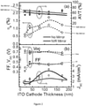
- Figure 1(c) is a graph showing the extinction coefficient, k , of the active layers shown in Figures 1(a) and 1(b).
- Figure 1(d) is a graph showing the current-voltage ( J-V ) curves for the ClAlPc-C 60 control and transparent cells of Figures 1(a) and 1(b) for a range of thicknesses of ITO.
- the absorption peak for ClAlPc is positioned in the NIR range ( ⁇ 740nm). This allows for the incorporation of a NIR reflecting mirror and simultaneous optimization of the solar cell performance and visible-transmissivity as diagramed in Figures 1(a) and 1(b) .
- the donor and/or acceptor layers may have one or more absorption peaks outside of the visual spectrum.
- the ClAlPc also has a second absorption peak in the UV range.
- Table 1 Cathode Thickness (nm) Cathode Composition Jsc (mA/cm 2 ) Voc (V) FF - Jsc (%) AVT (%) 100 Ag 4.7 0.77 0.55 2.4 0 20 ITO 1.5 0.69 0.39 0.5 67 120 ITO 3.2 0.71 0.46 1.3 65 20 ITO/NIR mir. 2.2 0.73 0.32 0.6 53 40 ITO/NIR mir. 2.5 0.71 0.49 1.1 55 80 ITO/NIR mir. 2.9 0.71 0.46 1.2 56 120 ITO/NIR mir. 4.4 0.71 0.44 1.7 56 170 ITO/NIR mir. 3.2 0.69 0.48 1.3 66
- Table 1 generally includes data showing the performance of control OPVs with an Ag cathode, transparent OPVs with ITO cathode, and OPVs with ITO cathode and NIR mirror, at 0.8 sun illumination corrected for solar spectrum mismatch.
- FIG. 2(b) is a graph showing photocurrent increase by a factor of 3x at an optimum thickness of 120nm so that ⁇ p increases by nearly the same amount. Fitting this data with the optical interference model shows that this behavior stems from interference of the backside ITO cathode reflection.
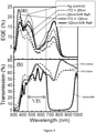
- Figure 3(a) is a graph showing EQE as a function of wavelength for several thicknesses of ITO and control layers with and without NIR reflecting mirrors. The approximate visible photopic range is highlighted by vertical dashed lines.
- Figure 3(b) is a graph showing transmission % as a function of wavelength for several thicknesses of ITO and control layers. Comparing EQE and transmission of the ITO-only devices, the absorption for the thinnest and optimized thicknesses appears equivalent. Inspection of the simulations shows, however, that the NIR field distribution is shifted from within the ITO anode to the ClAlPc active layer as the ITO cathode thickness increases, so that the total transmission appears the same even though the active layer absorption changes substantially. This highlights an important aspect of transparent OPV architectures; despite the seemingly simple optical configuration, interference management is still crucial to device optimization, particularly for NIR absorbing cells and for materials with low exciton diffusion lengths.
- the average visible transmissivity (AVT) shows little variation with ITO thickness (see e.g., Figure 2(a) ).
- the optical model predicts a slight decrease in AVT with ITO thicknesses that is not observed experimentally possibly due to model parameter uncertainties or varying optical constants during thicker ITO growths.
- Optimized cells without the NIR mirror show min (max) transmission values of 50% (74%) at 450nm (540nm) and an AVT of 65% (standard deviation of 7%).
- Figure 3(c) shows the measured solar simulator spectrum (left axis) exhibiting characteristics of the Xe-lamp and NREL reported mc-Si external quantum efficiency (EQE) for the reference-diode used to measure the solar simulator intensity (right-axis). Because the responsivity of the reference diode extends significantly beyond the response of the OPV cell, the extra NIR light from the solar simulator (compared to the AM1.5G spectrum) results in solar mismatch factors less than 1.
- Figure 3(d) shows the measured (left axis, circles) and calculated (left axis, solid line) reflectivity of the distributed Bragg reflector used in this study as the transparent, NIR mirror. Also shown is the transmission spectrum (right-axis) of the broad-band antireflection (BBAR) coatings.
- EQE mc-Si external quantum efficiency
- Figures 4a and 4b show solar cell arrays in front of a picture of a "rose". Both picture-detail and color-clarity are minimally disrupted so that details of the device array pattern are even difficult to discern.
- the array has a common cathode 25a and a plurality of anodes 22a.
- the device also includes an active area 30 which includes the donor layer(s), acceptor layer(s) and reflective mirrors.
- an array of 10 individual OPV devices is formed on the substrate 21a.
- Figure 4(c) shows the array wired to power an LCD clock.
- Figures 4(d) and 4(e) show an alternate embodiment of a solar cell array positioned in front of a picture of a "mountain" to highlight the transparency of the fully assembled device.
- Figure 4(f) is a picture of a full circuit assembly (left). Electrical connections are made to the ITO contacts of the OPV device (array) via carbon-tape.
- the LCD clock is connected to circuitry (right) that limits the voltage and passes excess current to a small LED such that the clock works under a wide range of OPV illumination conditions.
- the LCD clock requires approximately 1.5V and 10 ⁇ A and can be run by the solar cell for intensities ⁇ 0.05 suns (note that under the ambient lighting ⁇ 0.01 sun, the clock is off).
- the optimized power efficiency is nearly triple that of an existing visible-absorbing, semi-transparent, copper phthalocyanine planar device while also exhibiting 30% more average transmission, but is slightly less efficient (0.75x) than semi-transparent bulk-heterojunction structures that gain efficiency from active layer absorption in the visible and subsequently have nearly half the transmission.
- SnPc e.g., SnPc-C 60
- SnPc-C 60 may be used to construct transparent solar cells.
- Solar cell designs based on SnPc may achieve >2% efficient solar cell with >70% transmission of visible light ( ⁇ 70% average transmission across visible spectrum).
- the following layers were used in this example: ITO / SnPc(10nm) / C60(30nm) / BCP(10nm) / ITO(10nm) / DBR.
- the ITO was sputtered directly.
- the distributed Bragg reflectors (DBR) were applied with index matching fluid (IMF).
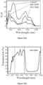
- Figure 5(a) is a graph showing the EQE as a function of wavelength for the SnPc device.
- Figure 5(b) is a graph showing transmissivity as a function of wavelength for the full TOPV SnPc device.
- Table 2 Cathode Jsc Voc FF ⁇ (%) Ag 6.15 0.40 0.55 1.3 ITO 1.54 0.33 0.48 0.2 ITO-DBR 2.25 0.34 0.44 0.3
- the device may include a NIR mirror (transparent to visible light) composed of either metal/oxide (e.g. TiO 2 /Ag/TiO 2 ) or dielectric stacks (DBRs e.g. consisting of SiO 2 /TiO 2 ).
- Anti-reflection coatings may be composed of single or multilayer dielectric materials.
- the molecular active layer may also be composed of any suitable phthalocyanine, porphyrin, naphthalocyanine dye, carbon nanotube, or molecular excitonic materials with absorption peaks outside of the visible spectrum.
- Figure 6(a) is a graph showing a comparison between SnPc and ClAlPc reference (opaque) designs.
- Table 3 Donor Thick Jsc Voc FF n (%) SnPc 100 6.15 0.40 0.50 1.2 ClAlPc 200 4.70 0.77 0.55 2.0
- Figure 6(b) is a graph showing the electric field and the effect of ITO cathode thickness.
- 2 Calculated optical field,
- Figures 6(c) and 6(d) show the transfer matrix simulations of the average visible transmission (AVT, left column) and short-circuit current (right column) of the transparent OPV architecture as a function of the anode and cathode ITO thicknesses without a NIR mirror.
- Figures 6(e) and 6(f) show the transfer matrix simulations of the average visible transmission (AVT, left column) and short-circuit current (right column) of the transparent OPV architecture as a function of the anode and cathode ITO thicknesses with a NIR mirror.
- the vertical dashed line indicates the thickness of the ITO anode utilized in this study.
- the active layer structure was Anode/MoO 3 (20nm) / ClAlPc(15nm) / C 60 (30nm) / BCP(7.5nm) / Cathode where the exciton diffusion lengths of ClAlPc and C 60 were estimated from fitting the magnitudes of the photocurrent and EQE of the control cell to be 8 ⁇ 4nm and 15 ⁇ 6nm, respectively.
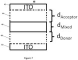
- the structure shown in Figure 1(b) includes discrete layers for the donor, e.g., ClAlPc or SnPc, and the acceptor, e.g., C 60 .
- the donor and acceptor may be combined in a single or mixed layer as shown generally in Figure 7 .
- the device 40 may have a mixed layer 46 including both a donor and an acceptor.
- the mixed layer generally has a thickness d mixed as shown.
- the device 40 may optionally include a discrete donor layer 48 and/or acceptor layer 46.
- the donor layer 48 if present, has a thickness d Donor as shown.
- the acceptor 46 layer if present, has a thickness d Acceptor as shown.
- the device 40 also includes a transparent cathode 42 and a transparent anode 50.
- the thicknesses of each layer may be selected as generally outlined above. It should be understood that such a structure may also include other layers including anti-reflective layers and mirror layers as disclosed in the various embodiments herein.
- An optimization process may generally be performed as follows:
- optimization may include an adjustment of the thickness of the mixed layer (step iii) and an adjustment of the ratio d Donor :d Acceptor (step vi).
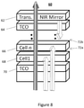
- FIG 8 is a block diagram of a tandem device 60.
- the device 60 generally includes at least a first and second cell 66, 68. Each cell may have the structure generally disclosed above. Each of the first and second cells 66, 68 function has transparent subcells. Each may have a varying NIR spectral responsivity. Each of the first and second cells may have absorption peaks at wavelengths outside of the visible light spectrum.
- a recombination zone 72a is disposed between the first and second cells 66, 68.
- the recombination zone may be composed of a variety of compounds including, e.g., ITO(0.5-10nm), or BCP/Ag(0.1-2nm)/ MoOx.
- the device 60 also includes a cathode 62 and an anode 70.
- the device may optionally include a transparent NIR mirror 62.
- Figures 9(a) and 9(b) are graphs showing different bandgaps associated with materials that may be used to optimize a device, e.g., US J. Aggregate ( Figure 9(a) ) and carbon nanotubes ( Figure 9(b) ).
- multiple bandgaps may be selected for successive layers stacked in a tandem device in order to yield a device with the desired efficiency.
- overall transparency is improved over devices that are independently fabricated and post integrated or macroscopically combined. This is possible because such a device benefits from a closely matched index of refraction at each interface between successive layers.
- the stacked structure may be transparent or semi-transparent.
- Figures 10(a) and 10(b) are graphs showing practical efficiency limits of several of the embodiments disclosed herein.
- Figure 11 is a diagram showing solar flux and the photopic response of the human eye. In general, the photopic response of the human eye peaks in the green spectrum 530-500nm and tapers off below 450nm and above 650nm.
- Figure 12 is a diagram showing an e-reader 80, smart phone 82 and display screen 84 including photovoltaic arrays 86, 88 and 90 disposed on their respective display screens. It should be understood that a variety of devices may incorporate the photovoltaic devices disclosed herein and/or arrays of such devices. Other applications include watch crystals, automotive and architectural glass including sunroofs and privacy glass. The photovoltaic devices may be used for active power generation, e.g., for completely self-powered applications and battery charging (or battery life extension).
Landscapes
- Physics & Mathematics (AREA)
- Electromagnetism (AREA)
- Chemical & Material Sciences (AREA)
- Inorganic Chemistry (AREA)
- Photovoltaic Devices (AREA)
- Electrochromic Elements, Electrophoresis, Or Variable Reflection Or Absorption Elements (AREA)
- Electric Clocks (AREA)
- Electromechanical Clocks (AREA)
Claims (12)
- Cellule photovoltaïque transparente (20), comprenant :un substrat transparent (21) ;une anode transparente (22) recouvrant le substrat transparent (21) ;un premier matériau actif transparent (23) recouvrant l'anode transparente (22), le premier matériau actif transparent (23) ayant un pic d'absorption à une longueur d'onde supérieure à 650 nanomètres ;un deuxième matériau actif transparent (24) recouvrant l'anode transparente (22), le deuxième matériau actif transparent (24) ayant un pic d'absorption à une longueur d'onde à l'extérieur du spectre de lumière visible ;une cathode transparente (25) recouvrant le substrat transparent (21), l'anode transparente (22) et les premier et deuxième matériaux actifs transparents (23, 24), le premier matériau actif transparent et le deuxième matériau actif transparent étant positionnés entre l'anode transparente et la cathode transparente ; etun miroir multicouche transparent à la lumière visible (62) recouvrant la cathode (25), configuré pour réfléchir à des longueurs d'onde dans le proche infrarouge ;dans laquelle transparent est une transparence visible moyenne à un faisceau rectiligne de 45 % ou plus.
- Cellule photovoltaïque transparente de la revendication 1, dans laquelle le premier matériau actif transparent (23) a un deuxième pic d'absorption à une longueur d'onde inférieure à 450 nanomètres.
- Cellule photovoltaïque transparente de la revendication 1, dans laquelle le premier matériau actif transparent (23) est un donneur et le deuxième matériau actif transparent (24) est un accepteur.
- Cellule photovoltaïque transparente de la revendication 1, dans laquelle le premier matériau actif transparent comprend un matériau organique.
- Cellule photovoltaïque transparente de la revendication 1, dans laquelle le premier matériau actif transparent comprend au moins un composé parmi : une phtalocyanine, une porphyrine, ou un colorant à base de naphtalocyanine.
- Cellule photovoltaïque transparente de la revendication 1, dans laquelle le premier matériau actif transparent comprend de la phtalocyanine de chloroaluminium.
- Cellule photovoltaïque transparente de la revendication 1, dans laquelle la première couche active transparente (23) comprend de la phtalocyanine d'étain.
- Cellule photovoltaïque transparente de la revendication 1, dans laquelle la deuxième couche active transparente (24) comprend du carbone 60 (O60) et/ou un nanotube.
- Cellule photovoltaïque transparente de la revendication 1, la cellule photovoltaïque (20) étant incorporée dans un écran d'affichage, ou un verre de montre, ou du verre pour l'automobile, ou du verre architectural.
- Réseau photovoltaïque transparent comprenant une pluralité de cellules voltaïques selon la revendication 1 interconnectées électriquement.
- Cellule photovoltaïque transparente de la revendication 1, dans laquelle le substrat transparent est souple.
- Procédé de production d'électricité, le procédé comprenant :l'obtention d'une cellule photovoltaïque transparente (20) comprenant :un substrat transparent (21) ;une anode transparente (22) recouvrant le substrat transparent (21) ;un premier matériau actif transparent (23) recouvrant l'anode transparente (22), le premier matériau actif transparent (23) ayant un pic d'absorption à une longueur d'onde supérieure à 650 nanomètres ;un deuxième matériau actif transparent (24) recouvrant l'anode transparente (22), le deuxième matériau actif transparent (24) ayant un pic d'absorption à une longueur d'onde à l'extérieur du spectre de lumière visible ;une cathode transparente (25) recouvrant le substrat transparent (21), l'anode transparente (22) et les premier et deuxième matériaux actifs transparents (23, 24), le premier matériau actif transparent et le deuxième matériau actif transparent étant positionnés entre l'anode transparente et la cathode transparente ; etun miroir multicouche transparent à la lumière visible (62) recouvrant la cathode, configuré pour réfléchir à des longueurs d'onde dans le proche infrarouge ; etl'exposition de la cellule photovoltaïque (20) à une source de lumière ; dans lequel transparent est une transparence visible moyenne à un faisceau rectiligne de 45 % ou plus.
Priority Applications (2)
| Application Number | Priority Date | Filing Date | Title |
|---|---|---|---|
| PL12701431T PL2668680T3 (pl) | 2011-01-26 | 2012-01-25 | Przezroczyste ogniwa fotowoltaiczne |
| EP21216267.1A EP4007003A1 (fr) | 2011-01-26 | 2012-01-25 | Cellules photovoltaïques transparentes |
Applications Claiming Priority (2)
| Application Number | Priority Date | Filing Date | Title |
|---|---|---|---|
| US201161436371P | 2011-01-26 | 2011-01-26 | |
| PCT/US2012/022543 WO2012103212A2 (fr) | 2011-01-26 | 2012-01-25 | Cellules photovoltaïques transparentes |
Related Child Applications (1)
| Application Number | Title | Priority Date | Filing Date |
|---|---|---|---|
| EP21216267.1A Division EP4007003A1 (fr) | 2011-01-26 | 2012-01-25 | Cellules photovoltaïques transparentes |
Publications (2)
| Publication Number | Publication Date |
|---|---|
| EP2668680A2 EP2668680A2 (fr) | 2013-12-04 |
| EP2668680B1 true EP2668680B1 (fr) | 2022-01-19 |
Family
ID=45541129
Family Applications (2)
| Application Number | Title | Priority Date | Filing Date |
|---|---|---|---|
| EP12701431.4A Active EP2668680B1 (fr) | 2011-01-26 | 2012-01-25 | Cellules photovoltaïques transparentes |
| EP21216267.1A Pending EP4007003A1 (fr) | 2011-01-26 | 2012-01-25 | Cellules photovoltaïques transparentes |
Family Applications After (1)
| Application Number | Title | Priority Date | Filing Date |
|---|---|---|---|
| EP21216267.1A Pending EP4007003A1 (fr) | 2011-01-26 | 2012-01-25 | Cellules photovoltaïques transparentes |
Country Status (14)
| Country | Link |
|---|---|
| US (4) | US9728735B2 (fr) |
| EP (2) | EP2668680B1 (fr) |
| JP (4) | JP2014505370A (fr) |
| KR (5) | KR102657521B1 (fr) |
| CN (2) | CN103534831A (fr) |
| AU (1) | AU2012209126B2 (fr) |
| BR (1) | BR112013019158B1 (fr) |
| CA (1) | CA2825584C (fr) |
| DK (1) | DK2668680T3 (fr) |
| ES (1) | ES2907221T3 (fr) |
| MX (1) | MX339751B (fr) |
| PL (1) | PL2668680T3 (fr) |
| RU (1) | RU2593915C2 (fr) |
| WO (1) | WO2012103212A2 (fr) |
Families Citing this family (49)
| Publication number | Priority date | Publication date | Assignee | Title |
|---|---|---|---|---|
| US9728735B2 (en) | 2011-01-26 | 2017-08-08 | Massachusetts Institute Of Technology | Transparent photovoltaic cells |
| US20130063493A1 (en) * | 2011-09-14 | 2013-03-14 | Htc Corporation | Devices and Methods Involving Display Interaction Using Photovoltaic Arrays |
| US20150122324A1 (en) * | 2012-05-18 | 2015-05-07 | Brookhaven Science Associates, Llc | Thin-film photovoltaic device with optical field confinement and method for making same |
| CN104718629A (zh) * | 2012-10-01 | 2015-06-17 | 无处不在能量公司 | 用于显示器或具有显示器的装置的波长选择性光电装置 |
| US10510914B2 (en) | 2013-03-21 | 2019-12-17 | Board Of Trustees Of Michigan State University | Transparent energy-harvesting devices |
| ES2785277T3 (es) * | 2013-04-30 | 2020-10-06 | Fundacio Inst De Ciencies Fotòniques | Dispositivo de fotoconversión semitransparente |
| EP2838095A1 (fr) | 2013-08-15 | 2015-02-18 | CSEM Centre Suisse d'Electronique et de Microtechnique SA - Recherche et Développement | Dispositif photovoltaïque de collecte de lumière |
| US9876184B2 (en) * | 2013-08-28 | 2018-01-23 | Taiwan Semiconductor Manufacturing Company, Ltd. | Organic photosensitive device with an electron-blocking and hole-transport layer |
| CN103531712B (zh) * | 2013-10-27 | 2016-03-16 | 中国乐凯集团有限公司 | 一种有机太阳能电池 |
| AU2015279582A1 (en) | 2014-06-27 | 2017-01-12 | The Administrators Of The Tulane Eductional Fund | Infrared transmissive concentrated photovoltaics for coupling solar electric energy conversion to solar thermal energy utilization |
| US10941612B2 (en) * | 2015-02-24 | 2021-03-09 | Lutron Technology Company Llc | Photovoltaic cells arranged in a pattern |
| DE112016001262T5 (de) * | 2015-03-18 | 2017-12-28 | Sumitomo Chemical Company, Limited | Vorrichtung zur photoelektrischen Umwandlung, die eine Reflexionsplatte aufweist |
| CN107851670B (zh) | 2015-04-27 | 2021-01-01 | 密歇根州立大学董事会 | 用于高电压有机和透明的太阳能电池的有机盐 |
| US10163166B1 (en) * | 2015-08-11 | 2018-12-25 | State Farm Mutual Automobile Insurance Company | Systems and methods for impact resistant and photovoltaic windows |
| US11489483B2 (en) | 2015-12-09 | 2022-11-01 | Brian Patrick Janowski | Solar window construction and methods |
| US11909352B2 (en) | 2016-03-28 | 2024-02-20 | The Administrators Of The Tulane Educational Fund | Transmissive concentrated photovoltaic module with cooling system |
| JP2020504456A (ja) * | 2017-01-10 | 2020-02-06 | ユビキタス エナジー, インコーポレイテッドUbiquitous Energy, Inc. | 窓一体型透明光起電力モジュール |
| US10651334B2 (en) | 2017-02-14 | 2020-05-12 | International Business Machines Corporation | Semitransparent chalcogen solar cell |
| CA3058410A1 (fr) * | 2017-02-24 | 2018-08-30 | The Administrators Of The Tulane Educational Fund | Systeme photovoltaique et photothermique solaire concentre |
| US10457148B2 (en) | 2017-02-24 | 2019-10-29 | Epic Battery Inc. | Solar car |
| JP2018161044A (ja) * | 2017-03-22 | 2018-10-11 | 住友化学株式会社 | 太陽光発電システム |
| CN106876594A (zh) * | 2017-03-31 | 2017-06-20 | 华南理工大学 | 一种半透明太阳电池器件及应用 |
| WO2018187384A1 (fr) | 2017-04-03 | 2018-10-11 | Epic Battery Inc. | Batterie solaire modulaire |
| WO2018209000A1 (fr) | 2017-05-09 | 2018-11-15 | Ubiqd Inc. | Éléments optiques luminescents pour applications agricoles |
| US11545635B2 (en) | 2017-06-16 | 2023-01-03 | Ubiquitous Energy, Inc. | Visibly transparent, near-infrared-absorbing boron-containing photovoltaic devices |
| US11778896B2 (en) | 2017-06-16 | 2023-10-03 | Ubiquitous Energy, Inc. | Visibly transparent, near-infrared-absorbing metal-complex photovoltaic devices |
| US11152581B2 (en) | 2017-06-16 | 2021-10-19 | Ubiquitous Energy, Inc. | Visibly transparent, near-infrared-absorbing donor/acceptor photovoltaic devices |
| US10903438B2 (en) | 2017-06-16 | 2021-01-26 | Ubiquitous Energy, Inc. | Visibly transparent, ultraviolet-absorbing photovoltaic devices |
| CN110944986A (zh) * | 2017-06-16 | 2020-03-31 | 无处不在能量公司 | 可见透明的近红外吸收性和紫外吸收性光伏装置 |
| US10992252B2 (en) | 2017-12-19 | 2021-04-27 | Universal Display Corporation | Integrated photovoltaic window and light source |
| US10613035B2 (en) * | 2018-01-17 | 2020-04-07 | Chromera, Inc. | Optically determining the condition of goods |
| US11061226B2 (en) | 2018-02-19 | 2021-07-13 | Honda Motor Co., Ltd. | Control of electrochromic pixels using integrated transparent photovoltaic converters and projected light for a transparent window display |
| WO2020056361A2 (fr) * | 2018-09-14 | 2020-03-19 | Ubiquitous Energy, Inc. | Procédé et système pour électrode transparente multicouche destinée à des dispositifs photovoltaïques transparents |
| US10926223B2 (en) * | 2019-04-11 | 2021-02-23 | Imam Abdulrahman Bin Faisal University | Apparatus for solar-assisted water distillation using waste heat of air conditioners |
| KR102693644B1 (ko) * | 2019-05-29 | 2024-08-08 | 노쓰 캐롤라이나 스테이트 유니버시티 | 단열 투명 탠덤 유기 태양 전지 |
| US11343257B2 (en) * | 2019-06-27 | 2022-05-24 | Microsoft Technology Licensing, Llc | Extended domain platform for nonmember user account management |
| US11489082B2 (en) | 2019-07-30 | 2022-11-01 | Epic Battery Inc. | Durable solar panels |
| CN114930541A (zh) | 2019-08-16 | 2022-08-19 | 无处不在能量公司 | 作为太阳能电池的缓冲和颜色调整层的对亚苯基材料 |
| JP2022544677A (ja) * | 2019-08-16 | 2022-10-20 | ユビキタス エナジー, インコーポレイテッド | 色中立透過太陽光発電のための方法及びシステム |
| RU196426U1 (ru) * | 2019-12-27 | 2020-02-28 | федеральное государственное автономное образовательное учреждение высшего образования "Национальный исследовательский университет ИТМО" (Университет ИТМО) | Прозрачный гетеропереход на основе оксидов |
| KR20210133493A (ko) * | 2020-04-29 | 2021-11-08 | 삼성전자주식회사 | 센서 및 전자 장치 |
| US20210359237A1 (en) * | 2020-05-15 | 2021-11-18 | Ubiquitous Energy, Inc. | Solar heat gain coefficient improvement by incorporating nir absorbers |
| NL2027206B1 (en) | 2020-12-22 | 2023-05-03 | Stichting Duurzame Energie Texel | Method of operating a solar energy system and solar energy system |
| CN112928216B (zh) * | 2021-02-03 | 2023-08-22 | 西湖大学 | 一种高透明度太阳能电池的制备方法 |
| CN113258004A (zh) * | 2021-04-16 | 2021-08-13 | 杭州电子科技大学 | 基于分布布拉格反射器的半透明太阳能电池及制备方法 |
| CN115707260A (zh) * | 2021-08-04 | 2023-02-17 | 隆基绿能科技股份有限公司 | 一种钙钛矿电池及光伏组件 |
| KR20240132257A (ko) * | 2022-01-03 | 2024-09-03 | 엘지전자 주식회사 | 투명 디스플레이 장치 |
| WO2024063840A2 (fr) * | 2022-07-16 | 2024-03-28 | Board Of Trustees Of Michigan State University | Photovoltaïque transparent multicouche à haut rendement basé sur un dépôt couche par couche |
| JP7540466B2 (ja) | 2022-08-01 | 2024-08-27 | トヨタ自動車株式会社 | 透明太陽電池が設置された窓構造 |
Citations (3)
| Publication number | Priority date | Publication date | Assignee | Title |
|---|---|---|---|---|
| WO1999039372A2 (fr) * | 1998-02-02 | 1999-08-05 | Uniax Corporation | Capteurs d'images fabriques a partir de semi-conducteurs organiques |
| US20090308456A1 (en) * | 2008-06-13 | 2009-12-17 | Interuniversitair Microelektronica Centrum (Imec) | Photovoltaic Structures and Method to Produce the Same |
| WO2010113606A1 (fr) * | 2009-03-31 | 2010-10-07 | リンテック株式会社 | Cellule solaire en couche mince organique et son procédé de fabrication |
Family Cites Families (31)
| Publication number | Priority date | Publication date | Assignee | Title |
|---|---|---|---|---|
| JPS63234567A (ja) * | 1987-03-24 | 1988-09-29 | Nippon Denso Co Ltd | 透光性太陽電池 |
| US5176758A (en) * | 1991-05-20 | 1993-01-05 | United Solar Systems Corporation | Translucent photovoltaic sheet material and panels |
| JPH05145096A (ja) * | 1991-11-22 | 1993-06-11 | Asahi Glass Co Ltd | 透過型太陽電池 |
| JP3006266B2 (ja) * | 1992-03-10 | 2000-02-07 | トヨタ自動車株式会社 | 太陽電池素子 |
| JP2001148491A (ja) | 1999-11-19 | 2001-05-29 | Fuji Xerox Co Ltd | 光電変換素子 |
| AU2001239934A1 (en) | 2000-04-27 | 2001-11-12 | Lgc Wireless, Inc. | Adaptive capacity management in a centralized basestation architecture |
| US6580027B2 (en) * | 2001-06-11 | 2003-06-17 | Trustees Of Princeton University | Solar cells using fullerenes |
| US20050081907A1 (en) * | 2003-10-20 | 2005-04-21 | Lewis Larry N. | Electro-active device having metal-containing layer |
| CA2551123A1 (fr) * | 2004-01-20 | 2005-07-28 | Cyrium Technologies Incorporated | Cellule solaire comportant une matiere a points quantiques obtenus par croissance epitaxiale |
| US7326955B2 (en) * | 2004-08-05 | 2008-02-05 | The Trustees Of Princeton University | Stacked organic photosensitive devices |
| US7375370B2 (en) * | 2004-08-05 | 2008-05-20 | The Trustees Of Princeton University | Stacked organic photosensitive devices |
| US7196366B2 (en) * | 2004-08-05 | 2007-03-27 | The Trustees Of Princeton University | Stacked organic photosensitive devices |
| US8592680B2 (en) * | 2004-08-11 | 2013-11-26 | The Trustees Of Princeton University | Organic photosensitive devices |
| JP4759286B2 (ja) | 2005-02-23 | 2011-08-31 | シャープ株式会社 | 有機太陽電池モジュール及びその製造方法 |
| JP4677314B2 (ja) * | 2005-09-20 | 2011-04-27 | 富士フイルム株式会社 | センサーおよび有機光電変換素子の駆動方法 |
| JP2009060051A (ja) * | 2007-09-03 | 2009-03-19 | National Institute Of Advanced Industrial & Technology | 有機太陽電池及び光センサ |
| US20090078316A1 (en) * | 2007-09-24 | 2009-03-26 | Qualcomm Incorporated | Interferometric photovoltaic cell |
| AU2007224388B8 (en) | 2007-09-28 | 2014-12-11 | The Regents Of The University Of Michigan | Organic photosensitive optoelectronic devices with near-infrared sensitivity |
| RU77505U1 (ru) * | 2008-05-15 | 2008-10-20 | Государственное образовательное учреждение высшего профессионального образования "Томский государственный университет систем управления и радиоэлектроники" (ГОУВПО "ТУСУР") | Фотоэлектрический элемент |
| RU2010152355A (ru) * | 2008-05-22 | 2012-06-27 | Коннектор Оптикс (Ru) | Способ для прикрепления оптических компонентов на интегральные схемы на основе кремния |
| JP2010041040A (ja) * | 2008-07-10 | 2010-02-18 | Semiconductor Energy Lab Co Ltd | 光電変換装置および光電変換装置の製造方法 |
| JP2010080908A (ja) * | 2008-08-29 | 2010-04-08 | Sumitomo Chemical Co Ltd | 有機光電変換素子およびその製造方法 |
| TWM349481U (en) * | 2008-09-05 | 2009-01-21 | Jin-Huai Yang | Photoelectric module |
| WO2010036963A1 (fr) * | 2008-09-26 | 2010-04-01 | The Regents Of The University Of Michigan | Cellules solaires organiques en tandem |
| JP5533646B2 (ja) * | 2009-01-20 | 2014-06-25 | 東レ株式会社 | 光起電力素子用材料および光起電力素子 |
| JP5667748B2 (ja) * | 2009-03-18 | 2015-02-12 | 株式会社東芝 | 光透過型太陽電池およびその製造方法 |
| US20100276071A1 (en) * | 2009-04-29 | 2010-11-04 | Solarmer Energy, Inc. | Tandem solar cell |
| EP2256839B1 (fr) * | 2009-05-28 | 2019-03-27 | IMEC vzw | Cellules photovoltaïques à une seule jonction ou multijonctions et procédé pour leur fabrication |
| WO2010141145A2 (fr) * | 2009-06-03 | 2010-12-09 | Massachusetts Institute Of Technology | Structure pseudo-périodique à utiliser dans des cellules solaires à couche mince |
| US11211559B2 (en) * | 2010-10-15 | 2021-12-28 | The Regents Of The University Of Michigan | Materials for controlling the epitaxial growth of photoactive layers in photovoltaic devices |
| US9728735B2 (en) | 2011-01-26 | 2017-08-08 | Massachusetts Institute Of Technology | Transparent photovoltaic cells |
-
2012
- 2012-01-25 US US13/358,075 patent/US9728735B2/en active Active
- 2012-01-25 KR KR1020227013716A patent/KR102657521B1/ko active IP Right Grant
- 2012-01-25 BR BR112013019158-9A patent/BR112013019158B1/pt active IP Right Grant
- 2012-01-25 WO PCT/US2012/022543 patent/WO2012103212A2/fr active Application Filing
- 2012-01-25 EP EP12701431.4A patent/EP2668680B1/fr active Active
- 2012-01-25 RU RU2013137652/28A patent/RU2593915C2/ru active
- 2012-01-25 KR KR1020137022193A patent/KR20140021542A/ko active Application Filing
- 2012-01-25 CN CN201280009604.1A patent/CN103534831A/zh active Pending
- 2012-01-25 KR KR1020247011828A patent/KR20240052995A/ko not_active Application Discontinuation
- 2012-01-25 DK DK12701431.4T patent/DK2668680T3/da active
- 2012-01-25 MX MX2013008573A patent/MX339751B/es active IP Right Grant
- 2012-01-25 KR KR1020197020057A patent/KR20190086040A/ko active Application Filing
- 2012-01-25 PL PL12701431T patent/PL2668680T3/pl unknown
- 2012-01-25 KR KR1020217003400A patent/KR102391529B1/ko active IP Right Grant
- 2012-01-25 JP JP2013551309A patent/JP2014505370A/ja active Pending
- 2012-01-25 ES ES12701431T patent/ES2907221T3/es active Active
- 2012-01-25 EP EP21216267.1A patent/EP4007003A1/fr active Pending
- 2012-01-25 CN CN201811126737.2A patent/CN109244247B/zh active Active
- 2012-01-25 AU AU2012209126A patent/AU2012209126B2/en active Active
- 2012-01-25 CA CA2825584A patent/CA2825584C/fr active Active
-
2017
- 2017-06-22 US US15/630,441 patent/US10665801B2/en active Active
- 2017-10-27 JP JP2017208415A patent/JP6576408B2/ja active Active
-
2019
- 2019-08-20 JP JP2019150143A patent/JP7101150B2/ja active Active
-
2020
- 2020-04-14 US US16/848,751 patent/US11424423B2/en active Active
-
2022
- 2022-07-04 JP JP2022107802A patent/JP2022153401A/ja active Pending
- 2022-07-15 US US17/866,362 patent/US20230052989A1/en active Pending
Patent Citations (4)
| Publication number | Priority date | Publication date | Assignee | Title |
|---|---|---|---|---|
| WO1999039372A2 (fr) * | 1998-02-02 | 1999-08-05 | Uniax Corporation | Capteurs d'images fabriques a partir de semi-conducteurs organiques |
| US20090308456A1 (en) * | 2008-06-13 | 2009-12-17 | Interuniversitair Microelektronica Centrum (Imec) | Photovoltaic Structures and Method to Produce the Same |
| WO2010113606A1 (fr) * | 2009-03-31 | 2010-10-07 | リンテック株式会社 | Cellule solaire en couche mince organique et son procédé de fabrication |
| EP2416393A1 (fr) * | 2009-03-31 | 2012-02-08 | LINTEC Corporation | Cellule solaire en couche mince organique et son procédé de fabrication |
Also Published As
Similar Documents
| Publication | Publication Date | Title |
|---|---|---|
| US11424423B2 (en) | Transparent photovoltaic cells | |
| Zhang et al. | Colorful semitransparent polymer solar cells employing a bottom periodic one-dimensional photonic crystal and a top conductive PEDOT: PSS layer | |
| EP2800161B1 (fr) | Dispositif de photoconversion semi-transparente | |
| Jiang et al. | Semitransparent organic solar cells based on all-low-bandgap donor and acceptor materials and their performance potential | |
| KR102170089B1 (ko) | 반사기를 지닌 유기 감광성 디바이스 | |
| CN113016078A (zh) | 用于透明光伏器件的多层透明电极的方法和系统 | |
| CN115244722A (zh) | 用于中性颜色的透光光伏器件的方法和系统 | |
| Çetinkaya | Efficient and high-bifacial CdTe-based solar cell enabled by functional designed dielectric/metal/dielectric transparent top contact via light management engineering | |
| US9748423B2 (en) | Photovoltaic device with fiber array for sun tracking | |
| Liu et al. | High-performance bifacial semitransparent organic photovoltaics featuring a decently transparent TeO 2/Ag electrode | |
| KR20190024589A (ko) | 컬러 필터링 전극을 포함하는 유기 태양전지, 및 상기 태양전지를 포함하는 스마트 윈도우 |
Legal Events
| Date | Code | Title | Description |
|---|---|---|---|
| PUAI | Public reference made under article 153(3) epc to a published international application that has entered the european phase |
Free format text: ORIGINAL CODE: 0009012 |
|
| 17P | Request for examination filed |
Effective date: 20130822 |
|
| AK | Designated contracting states |
Kind code of ref document: A2 Designated state(s): AL AT BE BG CH CY CZ DE DK EE ES FI FR GB GR HR HU IE IS IT LI LT LU LV MC MK MT NL NO PL PT RO RS SE SI SK SM TR |
|
| RIN1 | Information on inventor provided before grant (corrected) |
Inventor name: LUNT, RICHARD, ROYAL Inventor name: BULOVIC, VLADIMIR |
|
| DAX | Request for extension of the european patent (deleted) | ||
| REG | Reference to a national code |
Ref country code: HK Ref legal event code: DE Ref document number: 1192649 Country of ref document: HK |
|
| STAA | Information on the status of an ep patent application or granted ep patent |
Free format text: STATUS: EXAMINATION IS IN PROGRESS |
|
| 17Q | First examination report despatched |
Effective date: 20170915 |
|
| STAA | Information on the status of an ep patent application or granted ep patent |
Free format text: STATUS: EXAMINATION IS IN PROGRESS |
|
| GRAP | Despatch of communication of intention to grant a patent |
Free format text: ORIGINAL CODE: EPIDOSNIGR1 |
|
| STAA | Information on the status of an ep patent application or granted ep patent |
Free format text: STATUS: GRANT OF PATENT IS INTENDED |
|
| RIC1 | Information provided on ipc code assigned before grant |
Ipc: B82Y 10/00 20110101ALI20210205BHEP Ipc: H01L 27/30 20060101ALI20210205BHEP Ipc: H01L 51/42 20060101AFI20210205BHEP Ipc: H01L 51/44 20060101ALI20210205BHEP |
|
| INTG | Intention to grant announced |
Effective date: 20210316 |
|
| GRAJ | Information related to disapproval of communication of intention to grant by the applicant or resumption of examination proceedings by the epo deleted |
Free format text: ORIGINAL CODE: EPIDOSDIGR1 |
|
| STAA | Information on the status of an ep patent application or granted ep patent |
Free format text: STATUS: EXAMINATION IS IN PROGRESS |
|
| GRAP | Despatch of communication of intention to grant a patent |
Free format text: ORIGINAL CODE: EPIDOSNIGR1 |
|
| INTC | Intention to grant announced (deleted) | ||
| STAA | Information on the status of an ep patent application or granted ep patent |
Free format text: STATUS: GRANT OF PATENT IS INTENDED |
|
| INTG | Intention to grant announced |
Effective date: 20210826 |
|
| GRAS | Grant fee paid |
Free format text: ORIGINAL CODE: EPIDOSNIGR3 |
|
| STAA | Information on the status of an ep patent application or granted ep patent |
Free format text: STATUS: GRANT OF PATENT IS INTENDED |
|
| GRAA | (expected) grant |
Free format text: ORIGINAL CODE: 0009210 |
|
| STAA | Information on the status of an ep patent application or granted ep patent |
Free format text: STATUS: THE PATENT HAS BEEN GRANTED |
|
| AK | Designated contracting states |
Kind code of ref document: B1 Designated state(s): AL AT BE BG CH CY CZ DE DK EE ES FI FR GB GR HR HU IE IS IT LI LT LU LV MC MK MT NL NO PL PT RO RS SE SI SK SM TR |
|
| REG | Reference to a national code |
Ref country code: GB Ref legal event code: FG4D |
|
| REG | Reference to a national code |
Ref country code: CH Ref legal event code: EP |
|
| REG | Reference to a national code |
Ref country code: DE Ref legal event code: R096 Ref document number: 602012077546 Country of ref document: DE |
|
| REG | Reference to a national code |
Ref country code: AT Ref legal event code: REF Ref document number: 1464301 Country of ref document: AT Kind code of ref document: T Effective date: 20220215 |
|
| REG | Reference to a national code |
Ref country code: IE Ref legal event code: FG4D |
|
| REG | Reference to a national code |
Ref country code: DK Ref legal event code: T3 Effective date: 20220317 |
|
| REG | Reference to a national code |
Ref country code: FI Ref legal event code: FGE |
|
| REG | Reference to a national code |
Ref country code: ES Ref legal event code: FG2A Ref document number: 2907221 Country of ref document: ES Kind code of ref document: T3 Effective date: 20220422 |
|
| REG | Reference to a national code |
Ref country code: LT Ref legal event code: MG9D |
|
| REG | Reference to a national code |
Ref country code: NL Ref legal event code: MP Effective date: 20220119 |
|
| REG | Reference to a national code |
Ref country code: AT Ref legal event code: MK05 Ref document number: 1464301 Country of ref document: AT Kind code of ref document: T Effective date: 20220119 |
|
| PG25 | Lapsed in a contracting state [announced via postgrant information from national office to epo] |
Ref country code: NL Free format text: LAPSE BECAUSE OF FAILURE TO SUBMIT A TRANSLATION OF THE DESCRIPTION OR TO PAY THE FEE WITHIN THE PRESCRIBED TIME-LIMIT Effective date: 20220119 |
|
| PG25 | Lapsed in a contracting state [announced via postgrant information from national office to epo] |
Ref country code: SE Free format text: LAPSE BECAUSE OF FAILURE TO SUBMIT A TRANSLATION OF THE DESCRIPTION OR TO PAY THE FEE WITHIN THE PRESCRIBED TIME-LIMIT Effective date: 20220119 Ref country code: RS Free format text: LAPSE BECAUSE OF FAILURE TO SUBMIT A TRANSLATION OF THE DESCRIPTION OR TO PAY THE FEE WITHIN THE PRESCRIBED TIME-LIMIT Effective date: 20220119 Ref country code: PT Free format text: LAPSE BECAUSE OF FAILURE TO SUBMIT A TRANSLATION OF THE DESCRIPTION OR TO PAY THE FEE WITHIN THE PRESCRIBED TIME-LIMIT Effective date: 20220519 Ref country code: NO Free format text: LAPSE BECAUSE OF FAILURE TO SUBMIT A TRANSLATION OF THE DESCRIPTION OR TO PAY THE FEE WITHIN THE PRESCRIBED TIME-LIMIT Effective date: 20220419 Ref country code: LT Free format text: LAPSE BECAUSE OF FAILURE TO SUBMIT A TRANSLATION OF THE DESCRIPTION OR TO PAY THE FEE WITHIN THE PRESCRIBED TIME-LIMIT Effective date: 20220119 Ref country code: HR Free format text: LAPSE BECAUSE OF FAILURE TO SUBMIT A TRANSLATION OF THE DESCRIPTION OR TO PAY THE FEE WITHIN THE PRESCRIBED TIME-LIMIT Effective date: 20220119 Ref country code: BG Free format text: LAPSE BECAUSE OF FAILURE TO SUBMIT A TRANSLATION OF THE DESCRIPTION OR TO PAY THE FEE WITHIN THE PRESCRIBED TIME-LIMIT Effective date: 20220419 |
|
| PG25 | Lapsed in a contracting state [announced via postgrant information from national office to epo] |
Ref country code: LV Free format text: LAPSE BECAUSE OF FAILURE TO SUBMIT A TRANSLATION OF THE DESCRIPTION OR TO PAY THE FEE WITHIN THE PRESCRIBED TIME-LIMIT Effective date: 20220119 Ref country code: GR Free format text: LAPSE BECAUSE OF FAILURE TO SUBMIT A TRANSLATION OF THE DESCRIPTION OR TO PAY THE FEE WITHIN THE PRESCRIBED TIME-LIMIT Effective date: 20220420 Ref country code: AT Free format text: LAPSE BECAUSE OF FAILURE TO SUBMIT A TRANSLATION OF THE DESCRIPTION OR TO PAY THE FEE WITHIN THE PRESCRIBED TIME-LIMIT Effective date: 20220119 |
|
| PG25 | Lapsed in a contracting state [announced via postgrant information from national office to epo] |
Ref country code: IS Free format text: LAPSE BECAUSE OF FAILURE TO SUBMIT A TRANSLATION OF THE DESCRIPTION OR TO PAY THE FEE WITHIN THE PRESCRIBED TIME-LIMIT Effective date: 20220519 |
|
| REG | Reference to a national code |
Ref country code: DE Ref legal event code: R097 Ref document number: 602012077546 Country of ref document: DE |
|
| PG25 | Lapsed in a contracting state [announced via postgrant information from national office to epo] |
Ref country code: SM Free format text: LAPSE BECAUSE OF FAILURE TO SUBMIT A TRANSLATION OF THE DESCRIPTION OR TO PAY THE FEE WITHIN THE PRESCRIBED TIME-LIMIT Effective date: 20220119 Ref country code: SK Free format text: LAPSE BECAUSE OF FAILURE TO SUBMIT A TRANSLATION OF THE DESCRIPTION OR TO PAY THE FEE WITHIN THE PRESCRIBED TIME-LIMIT Effective date: 20220119 Ref country code: RO Free format text: LAPSE BECAUSE OF FAILURE TO SUBMIT A TRANSLATION OF THE DESCRIPTION OR TO PAY THE FEE WITHIN THE PRESCRIBED TIME-LIMIT Effective date: 20220119 Ref country code: MC Free format text: LAPSE BECAUSE OF FAILURE TO SUBMIT A TRANSLATION OF THE DESCRIPTION OR TO PAY THE FEE WITHIN THE PRESCRIBED TIME-LIMIT Effective date: 20220119 Ref country code: LU Free format text: LAPSE BECAUSE OF NON-PAYMENT OF DUE FEES Effective date: 20220125 Ref country code: EE Free format text: LAPSE BECAUSE OF FAILURE TO SUBMIT A TRANSLATION OF THE DESCRIPTION OR TO PAY THE FEE WITHIN THE PRESCRIBED TIME-LIMIT Effective date: 20220119 Ref country code: CZ Free format text: LAPSE BECAUSE OF FAILURE TO SUBMIT A TRANSLATION OF THE DESCRIPTION OR TO PAY THE FEE WITHIN THE PRESCRIBED TIME-LIMIT Effective date: 20220119 |
|
| PLBE | No opposition filed within time limit |
Free format text: ORIGINAL CODE: 0009261 |
|
| REG | Reference to a national code |
Ref country code: DE Ref legal event code: R079 Ref document number: 602012077546 Country of ref document: DE Free format text: PREVIOUS MAIN CLASS: H01L0051420000 Ipc: H10K0030000000 |
|
| STAA | Information on the status of an ep patent application or granted ep patent |
Free format text: STATUS: NO OPPOSITION FILED WITHIN TIME LIMIT |
|
| PG25 | Lapsed in a contracting state [announced via postgrant information from national office to epo] |
Ref country code: AL Free format text: LAPSE BECAUSE OF FAILURE TO SUBMIT A TRANSLATION OF THE DESCRIPTION OR TO PAY THE FEE WITHIN THE PRESCRIBED TIME-LIMIT Effective date: 20220119 |
|
| 26N | No opposition filed |
Effective date: 20221020 |
|
| PG25 | Lapsed in a contracting state [announced via postgrant information from national office to epo] |
Ref country code: IE Free format text: LAPSE BECAUSE OF NON-PAYMENT OF DUE FEES Effective date: 20220125 |
|
| PG25 | Lapsed in a contracting state [announced via postgrant information from national office to epo] |
Ref country code: SI Free format text: LAPSE BECAUSE OF FAILURE TO SUBMIT A TRANSLATION OF THE DESCRIPTION OR TO PAY THE FEE WITHIN THE PRESCRIBED TIME-LIMIT Effective date: 20220119 |
|
| P01 | Opt-out of the competence of the unified patent court (upc) registered |
Effective date: 20230528 |
|
| PG25 | Lapsed in a contracting state [announced via postgrant information from national office to epo] |
Ref country code: HU Free format text: LAPSE BECAUSE OF FAILURE TO SUBMIT A TRANSLATION OF THE DESCRIPTION OR TO PAY THE FEE WITHIN THE PRESCRIBED TIME-LIMIT; INVALID AB INITIO Effective date: 20120125 |
|
| PGFP | Annual fee paid to national office [announced via postgrant information from national office to epo] |
Ref country code: ES Payment date: 20240201 Year of fee payment: 13 |
|
| PG25 | Lapsed in a contracting state [announced via postgrant information from national office to epo] |
Ref country code: MK Free format text: LAPSE BECAUSE OF FAILURE TO SUBMIT A TRANSLATION OF THE DESCRIPTION OR TO PAY THE FEE WITHIN THE PRESCRIBED TIME-LIMIT Effective date: 20220119 Ref country code: CY Free format text: LAPSE BECAUSE OF FAILURE TO SUBMIT A TRANSLATION OF THE DESCRIPTION OR TO PAY THE FEE WITHIN THE PRESCRIBED TIME-LIMIT Effective date: 20220119 |
|
| PGFP | Annual fee paid to national office [announced via postgrant information from national office to epo] |
Ref country code: FI Payment date: 20240125 Year of fee payment: 13 Ref country code: DE Payment date: 20240129 Year of fee payment: 13 Ref country code: CH Payment date: 20240202 Year of fee payment: 13 Ref country code: GB Payment date: 20240129 Year of fee payment: 13 |
|
| PGFP | Annual fee paid to national office [announced via postgrant information from national office to epo] |
Ref country code: TR Payment date: 20240119 Year of fee payment: 13 Ref country code: PL Payment date: 20240109 Year of fee payment: 13 Ref country code: IT Payment date: 20240122 Year of fee payment: 13 Ref country code: FR Payment date: 20240125 Year of fee payment: 13 Ref country code: DK Payment date: 20240125 Year of fee payment: 13 Ref country code: BE Payment date: 20240129 Year of fee payment: 13 |
|
| PG25 | Lapsed in a contracting state [announced via postgrant information from national office to epo] |
Ref country code: MT Free format text: LAPSE BECAUSE OF FAILURE TO SUBMIT A TRANSLATION OF THE DESCRIPTION OR TO PAY THE FEE WITHIN THE PRESCRIBED TIME-LIMIT Effective date: 20220119 |