EP2668680B1 - Transparent photovoltaic cells - Google Patents
Transparent photovoltaic cells Download PDFInfo
- Publication number
- EP2668680B1 EP2668680B1 EP12701431.4A EP12701431A EP2668680B1 EP 2668680 B1 EP2668680 B1 EP 2668680B1 EP 12701431 A EP12701431 A EP 12701431A EP 2668680 B1 EP2668680 B1 EP 2668680B1
- Authority
- EP
- European Patent Office
- Prior art keywords
- transparent
- active material
- photovoltaic cell
- anode
- overlying
- Prior art date
- Legal status (The legal status is an assumption and is not a legal conclusion. Google has not performed a legal analysis and makes no representation as to the accuracy of the status listed.)
- Active
Links
- 238000010521 absorption reaction Methods 0.000 claims description 29
- 239000011149 active material Substances 0.000 claims description 27
- LBGCRGLFTKVXDZ-UHFFFAOYSA-M ac1mc2aw Chemical compound [Al+3].[Cl-].C12=CC=CC=C2C(N=C2[N-]C(C3=CC=CC=C32)=N2)=NC1=NC([C]1C=CC=CC1=1)=NC=1N=C1[C]3C=CC=CC3=C2[N-]1 LBGCRGLFTKVXDZ-UHFFFAOYSA-M 0.000 claims description 23
- 239000000758 substrate Substances 0.000 claims description 16
- 238000001228 spectrum Methods 0.000 claims description 15
- 239000011521 glass Substances 0.000 claims description 6
- IEQIEDJGQAUEQZ-UHFFFAOYSA-N phthalocyanine Chemical compound N1C(N=C2C3=CC=CC=C3C(N=C3C4=CC=CC=C4C(=N4)N3)=N2)=C(C=CC=C2)C2=C1N=C1C2=CC=CC=C2C4=N1 IEQIEDJGQAUEQZ-UHFFFAOYSA-N 0.000 claims description 6
- OKTJSMMVPCPJKN-UHFFFAOYSA-N Carbon Chemical compound [C] OKTJSMMVPCPJKN-UHFFFAOYSA-N 0.000 claims description 5
- 239000005328 architectural glass Substances 0.000 claims description 4
- 238000000034 method Methods 0.000 claims description 4
- 150000004032 porphyrins Chemical class 0.000 claims description 4
- 239000013078 crystal Substances 0.000 claims description 3
- 239000002071 nanotube Substances 0.000 claims description 3
- LKKPNUDVOYAOBB-UHFFFAOYSA-N naphthalocyanine Chemical compound N1C(N=C2C3=CC4=CC=CC=C4C=C3C(N=C3C4=CC5=CC=CC=C5C=C4C(=N4)N3)=N2)=C(C=C2C(C=CC=C2)=C2)C2=C1N=C1C2=CC3=CC=CC=C3C=C2C4=N1 LKKPNUDVOYAOBB-UHFFFAOYSA-N 0.000 claims description 3
- ATJFFYVFTNAWJD-UHFFFAOYSA-N Tin Chemical compound [Sn] ATJFFYVFTNAWJD-UHFFFAOYSA-N 0.000 claims description 2
- 229910052799 carbon Inorganic materials 0.000 claims description 2
- 239000011368 organic material Substances 0.000 claims description 2
- 230000005611 electricity Effects 0.000 claims 1
- 239000010410 layer Substances 0.000 description 63
- 230000005540 biological transmission Effects 0.000 description 25
- 238000013086 organic photovoltaic Methods 0.000 description 18
- JKQOBWVOAYFWKG-UHFFFAOYSA-N molybdenum trioxide Chemical compound O=[Mo](=O)=O JKQOBWVOAYFWKG-UHFFFAOYSA-N 0.000 description 14
- 238000000576 coating method Methods 0.000 description 8
- 239000000463 material Substances 0.000 description 8
- 238000010586 diagram Methods 0.000 description 7
- 230000003287 optical effect Effects 0.000 description 7
- VYPSYNLAJGMNEJ-UHFFFAOYSA-N silicon dioxide Inorganic materials O=[Si]=O VYPSYNLAJGMNEJ-UHFFFAOYSA-N 0.000 description 7
- STTGYIUESPWXOW-UHFFFAOYSA-N 2,9-dimethyl-4,7-diphenyl-1,10-phenanthroline Chemical compound C=12C=CC3=C(C=4C=CC=CC=4)C=C(C)N=C3C2=NC(C)=CC=1C1=CC=CC=C1 STTGYIUESPWXOW-UHFFFAOYSA-N 0.000 description 6
- -1 Poly(3,4-ethylenedioxythiophene) Polymers 0.000 description 6
- GWEVSGVZZGPLCZ-UHFFFAOYSA-N Titan oxide Chemical compound O=[Ti]=O GWEVSGVZZGPLCZ-UHFFFAOYSA-N 0.000 description 6
- 238000004088 simulation Methods 0.000 description 6
- 238000001429 visible spectrum Methods 0.000 description 6
- 238000006243 chemical reaction Methods 0.000 description 5
- 230000007423 decrease Effects 0.000 description 5
- 230000006798 recombination Effects 0.000 description 5
- 238000005215 recombination Methods 0.000 description 5
- 238000002310 reflectometry Methods 0.000 description 5
- 230000004044 response Effects 0.000 description 5
- XLOMVQKBTHCTTD-UHFFFAOYSA-N Zinc monoxide Chemical compound [Zn]=O XLOMVQKBTHCTTD-UHFFFAOYSA-N 0.000 description 4
- 238000003491 array Methods 0.000 description 4
- 238000010348 incorporation Methods 0.000 description 4
- 239000011159 matrix material Substances 0.000 description 4
- 238000005457 optimization Methods 0.000 description 4
- 239000004065 semiconductor Substances 0.000 description 4
- 238000012546 transfer Methods 0.000 description 4
- 229920001609 Poly(3,4-ethylenedioxythiophene) Polymers 0.000 description 3
- 239000002041 carbon nanotube Substances 0.000 description 3
- 229910021393 carbon nanotube Inorganic materials 0.000 description 3
- 238000009792 diffusion process Methods 0.000 description 3
- 230000001747 exhibiting effect Effects 0.000 description 3
- 238000005286 illumination Methods 0.000 description 3
- 239000010453 quartz Substances 0.000 description 3
- 241000220317 Rosa Species 0.000 description 2
- 230000008901 benefit Effects 0.000 description 2
- 230000008033 biological extinction Effects 0.000 description 2
- 229910052681 coesite Inorganic materials 0.000 description 2
- 238000001816 cooling Methods 0.000 description 2
- 229910052906 cristobalite Inorganic materials 0.000 description 2
- 230000000694 effects Effects 0.000 description 2
- 239000012530 fluid Substances 0.000 description 2
- 230000004907 flux Effects 0.000 description 2
- AMGQUBHHOARCQH-UHFFFAOYSA-N indium;oxotin Chemical compound [In].[Sn]=O AMGQUBHHOARCQH-UHFFFAOYSA-N 0.000 description 2
- 238000010248 power generation Methods 0.000 description 2
- 230000009467 reduction Effects 0.000 description 2
- 239000000377 silicon dioxide Substances 0.000 description 2
- 229910052682 stishovite Inorganic materials 0.000 description 2
- QHGNHLZPVBIIPX-UHFFFAOYSA-N tin(ii) oxide Chemical class [Sn]=O QHGNHLZPVBIIPX-UHFFFAOYSA-N 0.000 description 2
- 229910052905 tridymite Inorganic materials 0.000 description 2
- 239000011787 zinc oxide Substances 0.000 description 2
- GYHNNYVSQQEPJS-UHFFFAOYSA-N Gallium Chemical compound [Ga] GYHNNYVSQQEPJS-UHFFFAOYSA-N 0.000 description 1
- 229910015711 MoOx Inorganic materials 0.000 description 1
- 229920000144 PEDOT:PSS Polymers 0.000 description 1
- 238000000862 absorption spectrum Methods 0.000 description 1
- 229910052782 aluminium Inorganic materials 0.000 description 1
- XAGFODPZIPBFFR-UHFFFAOYSA-N aluminium Chemical compound [Al] XAGFODPZIPBFFR-UHFFFAOYSA-N 0.000 description 1
- 230000003667 anti-reflective effect Effects 0.000 description 1
- QVGXLLKOCUKJST-UHFFFAOYSA-N atomic oxygen Chemical compound [O] QVGXLLKOCUKJST-UHFFFAOYSA-N 0.000 description 1
- 150000001875 compounds Chemical class 0.000 description 1
- 238000012937 correction Methods 0.000 description 1
- 238000000151 deposition Methods 0.000 description 1
- 230000008021 deposition Effects 0.000 description 1
- 239000003989 dielectric material Substances 0.000 description 1
- 238000009826 distribution Methods 0.000 description 1
- 230000005684 electric field Effects 0.000 description 1
- 238000005538 encapsulation Methods 0.000 description 1
- 238000005265 energy consumption Methods 0.000 description 1
- 239000005357 flat glass Substances 0.000 description 1
- 229920005570 flexible polymer Polymers 0.000 description 1
- 229910052733 gallium Inorganic materials 0.000 description 1
- 230000012010 growth Effects 0.000 description 1
- RBTKNAXYKSUFRK-UHFFFAOYSA-N heliogen blue Chemical compound [Cu].[N-]1C2=C(C=CC=C3)C3=C1N=C([N-]1)C3=CC=CC=C3C1=NC([N-]1)=C(C=CC=C3)C3=C1N=C([N-]1)C3=CC=CC=C3C1=N2 RBTKNAXYKSUFRK-UHFFFAOYSA-N 0.000 description 1
- 238000007689 inspection Methods 0.000 description 1
- 238000011835 investigation Methods 0.000 description 1
- 238000005259 measurement Methods 0.000 description 1
- 229910052751 metal Inorganic materials 0.000 description 1
- 239000002184 metal Substances 0.000 description 1
- 239000000203 mixture Substances 0.000 description 1
- 239000012044 organic layer Substances 0.000 description 1
- 230000010355 oscillation Effects 0.000 description 1
- 229910052760 oxygen Inorganic materials 0.000 description 1
- 239000001301 oxygen Substances 0.000 description 1
- 229920001467 poly(styrenesulfonates) Polymers 0.000 description 1
- 230000008569 process Effects 0.000 description 1
- 230000001012 protector Effects 0.000 description 1
- 229910052709 silver Inorganic materials 0.000 description 1
- 239000004332 silver Substances 0.000 description 1
- 229910021649 silver-doped titanium dioxide Inorganic materials 0.000 description 1
- 150000003384 small molecules Chemical class 0.000 description 1
- 230000003595 spectral effect Effects 0.000 description 1
- 238000004544 sputter deposition Methods 0.000 description 1
- 238000000859 sublimation Methods 0.000 description 1
- 230000008022 sublimation Effects 0.000 description 1
- 238000002207 thermal evaporation Methods 0.000 description 1
- 239000010409 thin film Substances 0.000 description 1
- 229910001887 tin oxide Inorganic materials 0.000 description 1
- 238000000411 transmission spectrum Methods 0.000 description 1
- 230000000007 visual effect Effects 0.000 description 1
Images


Classifications
-
- H—ELECTRICITY
- H10—SEMICONDUCTOR DEVICES; ELECTRIC SOLID-STATE DEVICES NOT OTHERWISE PROVIDED FOR
- H10K—ORGANIC ELECTRIC SOLID-STATE DEVICES
- H10K30/00—Organic devices sensitive to infrared radiation, light, electromagnetic radiation of shorter wavelength or corpuscular radiation
- H10K30/10—Organic devices sensitive to infrared radiation, light, electromagnetic radiation of shorter wavelength or corpuscular radiation comprising heterojunctions between organic semiconductors and inorganic semiconductors
-
- H—ELECTRICITY
- H10—SEMICONDUCTOR DEVICES; ELECTRIC SOLID-STATE DEVICES NOT OTHERWISE PROVIDED FOR
- H10K—ORGANIC ELECTRIC SOLID-STATE DEVICES
- H10K30/00—Organic devices sensitive to infrared radiation, light, electromagnetic radiation of shorter wavelength or corpuscular radiation
- H10K30/20—Organic devices sensitive to infrared radiation, light, electromagnetic radiation of shorter wavelength or corpuscular radiation comprising organic-organic junctions, e.g. donor-acceptor junctions
- H10K30/211—Organic devices sensitive to infrared radiation, light, electromagnetic radiation of shorter wavelength or corpuscular radiation comprising organic-organic junctions, e.g. donor-acceptor junctions comprising multiple junctions, e.g. double heterojunctions
-
- H—ELECTRICITY
- H10—SEMICONDUCTOR DEVICES; ELECTRIC SOLID-STATE DEVICES NOT OTHERWISE PROVIDED FOR
- H10K—ORGANIC ELECTRIC SOLID-STATE DEVICES
- H10K30/00—Organic devices sensitive to infrared radiation, light, electromagnetic radiation of shorter wavelength or corpuscular radiation
- H10K30/50—Photovoltaic [PV] devices
- H10K30/57—Photovoltaic [PV] devices comprising multiple junctions, e.g. tandem PV cells
-
- H—ELECTRICITY
- H10—SEMICONDUCTOR DEVICES; ELECTRIC SOLID-STATE DEVICES NOT OTHERWISE PROVIDED FOR
- H10K—ORGANIC ELECTRIC SOLID-STATE DEVICES
- H10K30/00—Organic devices sensitive to infrared radiation, light, electromagnetic radiation of shorter wavelength or corpuscular radiation
- H10K30/80—Constructional details
- H10K30/87—Light-trapping means
-
- H—ELECTRICITY
- H10—SEMICONDUCTOR DEVICES; ELECTRIC SOLID-STATE DEVICES NOT OTHERWISE PROVIDED FOR
- H10K—ORGANIC ELECTRIC SOLID-STATE DEVICES
- H10K2102/00—Constructional details relating to the organic devices covered by this subclass
- H10K2102/301—Details of OLEDs
- H10K2102/351—Thickness
-
- H—ELECTRICITY
- H10—SEMICONDUCTOR DEVICES; ELECTRIC SOLID-STATE DEVICES NOT OTHERWISE PROVIDED FOR
- H10K—ORGANIC ELECTRIC SOLID-STATE DEVICES
- H10K30/00—Organic devices sensitive to infrared radiation, light, electromagnetic radiation of shorter wavelength or corpuscular radiation
- H10K30/30—Organic devices sensitive to infrared radiation, light, electromagnetic radiation of shorter wavelength or corpuscular radiation comprising bulk heterojunctions, e.g. interpenetrating networks of donor and acceptor material domains
-
- H—ELECTRICITY
- H10—SEMICONDUCTOR DEVICES; ELECTRIC SOLID-STATE DEVICES NOT OTHERWISE PROVIDED FOR
- H10K—ORGANIC ELECTRIC SOLID-STATE DEVICES
- H10K30/00—Organic devices sensitive to infrared radiation, light, electromagnetic radiation of shorter wavelength or corpuscular radiation
- H10K30/80—Constructional details
- H10K30/81—Electrodes
- H10K30/82—Transparent electrodes, e.g. indium tin oxide [ITO] electrodes
-
- Y—GENERAL TAGGING OF NEW TECHNOLOGICAL DEVELOPMENTS; GENERAL TAGGING OF CROSS-SECTIONAL TECHNOLOGIES SPANNING OVER SEVERAL SECTIONS OF THE IPC; TECHNICAL SUBJECTS COVERED BY FORMER USPC CROSS-REFERENCE ART COLLECTIONS [XRACs] AND DIGESTS
- Y02—TECHNOLOGIES OR APPLICATIONS FOR MITIGATION OR ADAPTATION AGAINST CLIMATE CHANGE
- Y02E—REDUCTION OF GREENHOUSE GAS [GHG] EMISSIONS, RELATED TO ENERGY GENERATION, TRANSMISSION OR DISTRIBUTION
- Y02E10/00—Energy generation through renewable energy sources
- Y02E10/50—Photovoltaic [PV] energy
- Y02E10/549—Organic PV cells
Definitions
- This invention relates to the field of photovoltaic devices and more particularly, organic photovoltaic devices.
- window glass utilized in automobiles and architecture are typically 70-80% and 55-90% transmissive, respectively, to the visible spectrum, e.g., light with wavelengths from about 450 to 650 nanometers (nm).
- OLED organic photovoltaic
- BAILEY-SALZMAN RHONDA ET AL "Near-infrared sensitive small molecule organic photovoltaic cells based on chloroaluminum phthalocyanine", ⁇ APPLIED PHYSICS LETTERS, AIP, AMERICAN INSTITUTE OF PHYSICS, MELVILLE, NY, US, vol. 91, no. 1, 5 July 2007 (2007-07-05), pages 13508-13508, XP012098993, ISSN: 0003-6951, DOI: 10.1063/1.2752992
- CHI-FENG LIN CHI-FENG LIN , MI ZHANG , SHUN-WEI LIU, TIEN-LUNG CHIU AND JIUN-HAW LEE: "High Photoelectric Conversion Efficiency of Metal Phthalocyanine / Fullerene Heterojunction Photovoltaic Device", INT. J. MOL. SCI., vol. 12, 17 January 2011 (2011-01-17), pages 476-505 , XP002675896
- the first active material may have a second absorption peak at a wavelength less than about 450 nanometers.
- the first active material may be a donor and the second active material may be an acceptor.
- the device includes a mirror reflecting at near infra-red wavelengths.
- the first active material may comprise an organic material.
- the first active material may comprise at least one of: a phthalocyanine, a porphyrin, or a naphthalocyanine dye.
- the first active material may comprise chloroaluminum phthalocyanine.
- the first active layer may comprise tin phthalocyanine.
- the second active layer may comprise at least one of carbon 60 (C60) or a nanotube.
- the first and second active materials may be configured for use with flexible encapsulation layers.
- the photovoltaic cell may include a recombination zone disposed between a first and second subcell, each of the first and second subcells having absorption peaks at wavelengths outside of the visible light spectrum, a transparent cathode and a transparent anode.
- TOPV transparent organic photovoltaic devices
- the term transparent as used herein encompasses an average visible transparency of a straight through beam of 45% or more.
- the term semi-transparent as used herein encompasses an average visible transparency of a straight through beam of approximately 10%-45%.
- the designs include molecular active layers with strong absorption features outside of the visible light spectrum, e.g., in the ultra-violet (UV) and/or near-infrared (NIR) solar spectrum.
- the devices may include selective high-reflectivity NIR and broadband anti-reflection contact coatings.
- Devices may be formed as heterojunction solar cells with an organic active layer, such as chloroaluminum phthalocyanine (ClAlPc) or SnPc as a donor and a molecular active layer such as C 60 acting as an acceptor and having peak-absorption in the UV and NIR solar spectrum.
- organic active layer such as chloroaluminum phthalocyanine (ClAlPc) or SnPc as a donor
- a molecular active layer such as C 60 acting as an acceptor and having peak-absorption in the UV and NIR solar spectrum.
- Other suitable materials for the active layers include any suitable phthalocyanine, porphyrin, naphthalocynanine dye, carbon nanotubes or molecular excitonic materials with absorption peaks outside the visible spectrum.
- Such devices may be formed in a tandem structure with one or more subcells joined via a recombination zone.
- Such devices may be used in a variety of applications including rigid and flexible computer display screens used in a desktop monitor, laptop or notebook computer, tablet computer, mobile phone, e-readers and the like.
- Other applications include watch crystals, automotive and architectural glass including sunroofs and privacy glass.
- the photovoltaic devices may be used for active power generation, e.g., for completely self-powered applications, and battery charging (or battery life extension).
- NIR Near-infrared
- UV Ultraviolet
- the use of an active layer having absorption in the NIR and the UV allows for the use of selective high-reflectivity near-infrared mirror coatings to optimize device performance while also permitting high transmission of visible light through the entire device.
- Visible light as recited herein is defined as light having wavelengths to which the human eye has a significant response, from about 450 to about 650 nm.
- devices were fabricated on 150nm of patterned Indium Tin Oxide (ITO) (15 ⁇ /sq.) pre-coated onto glass substrates.
- ITO Indium Tin Oxide
- the ITO is one component of an electrode.
- the ITO was solvent-cleaned and subsequently treated in oxygen plasma for 30 seconds immediately prior to loading into a high vacuum chamber ( ⁇ 1 ⁇ 10 -6 Torr, wherein 1 Torr is equal to 133,32 Pa) .
- ClAlPc and C 60 were purified once by vacuum train sublimation prior to loading.
- Bathocuproine (BCP) and molybdenum trioxide (MoO 3 ) were used as purchased.
- MoO 3 is another component of an electrode.
- the MoO 3 (20nm), ClAlPc (15nm), C 60 (30nm), BCP (7.5nm), and a 100nm thick Ag cathode were sequentially deposited via thermal evaporation at a rate of 0.1nm/s.
- the top ITO cathode for the transparent devices was rf-sputtered directly onto the organic layers at low power (7-25W) with 10 sccm Ar flow (6 mTorr) and 0.005-0.03nm/second.
- Cathodes were evaporated through a shadow mask, defining a 1 millimeter (mm) x 1.2 mm active device area.
- a near-infrared distributed Bragg reflector (DBR) utilized as the transparent NIR mirror was grown separately on quartz via sputtering of 7 alternating layers of TiO 2 and SiO 2 at about 0.1nm/second with thicknesses centered around a wavelength of 800nm (200nm stop band).
- Broad-band antireflection (BBAR) coatings precoated on quartz substrates (1-side) were attached to the DBRs via index matching fluid to reduce additional glass/air interface reflections. Transmission data of the assembled devices were obtained at normal incidence with a Cary Eclipse 5000 dual-beam spectrophotometer without reference samples.
- FIG. 1(a) shows a schematic of a control solar cell 10.
- the control solar cell includes a substrate 11, an anode 12, a donor layer 13 e.g., ClAlPc, a molecular active layer, e.g., C 60 , acting as an acceptor layer 14 and a cathode 15.
- the anode 15 is opaque, e.g., silver.
- Figure 1(b) shows a schematic of a full transparent solar cell 20.
- the device 20 generally includes a transparent substrate 21, an anode 22, a donor layer 23, e.g., ClAlPc, a molecular active layer, e.g., C 60 , acting as an acceptor layer 24, and a cathode 25.
- the donor layer 23 and the acceptor layer 24 have absorption peaks in the ultra-violet (UV) and near-infrared (NIR) spectrum.
- the substrate is quartz. It should be understood that a variety of rigid and flexible substrates may be used.
- the substrate may be glass, a rigid or flexible polymer, e.g., a screen protector or skin, or may be combined with other layers such as encapsulating layers, anti-reflecting layers or the like.
- the transparent anode 22 and cathode 25 are formed of conducting oxide, e.g. ITO/MoO 3 .
- anode 22 and cathode 25 may be formed of other materials such as tin oxides, fluorinated tin oxides, nanotubes, Poly(3,4-ethylenedioxythiophene) (PDOT) or PEDOT:PSS (Poly(3,4-ethylenedioxythiophene) poly(styrenesulfonate)), gallium doped zinc oxide, aluminum doped zinc oxide and other materials having suitable transparency and conductivity.
- the device 20 may also include a near-infrared DBR 26 and one or more broad-band antireflection (BBAR) coatings 27.
- BBAR broad-band antireflection
- Figure 1(c) is a graph showing the extinction coefficient, k , of the active layers shown in Figures 1(a) and 1(b).
- Figure 1(d) is a graph showing the current-voltage ( J-V ) curves for the ClAlPc-C 60 control and transparent cells of Figures 1(a) and 1(b) for a range of thicknesses of ITO.
- the absorption peak for ClAlPc is positioned in the NIR range ( ⁇ 740nm). This allows for the incorporation of a NIR reflecting mirror and simultaneous optimization of the solar cell performance and visible-transmissivity as diagramed in Figures 1(a) and 1(b) .
- the donor and/or acceptor layers may have one or more absorption peaks outside of the visual spectrum.
- the ClAlPc also has a second absorption peak in the UV range.
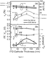
- Table 1 Cathode Thickness (nm) Cathode Composition Jsc (mA/cm 2 ) Voc (V) FF - Jsc (%) AVT (%) 100 Ag 4.7 0.77 0.55 2.4 0 20 ITO 1.5 0.69 0.39 0.5 67 120 ITO 3.2 0.71 0.46 1.3 65 20 ITO/NIR mir. 2.2 0.73 0.32 0.6 53 40 ITO/NIR mir. 2.5 0.71 0.49 1.1 55 80 ITO/NIR mir. 2.9 0.71 0.46 1.2 56 120 ITO/NIR mir. 4.4 0.71 0.44 1.7 56 170 ITO/NIR mir. 3.2 0.69 0.48 1.3 66
- Table 1 generally includes data showing the performance of control OPVs with an Ag cathode, transparent OPVs with ITO cathode, and OPVs with ITO cathode and NIR mirror, at 0.8 sun illumination corrected for solar spectrum mismatch.
- FIG. 2(b) is a graph showing photocurrent increase by a factor of 3x at an optimum thickness of 120nm so that ⁇ p increases by nearly the same amount. Fitting this data with the optical interference model shows that this behavior stems from interference of the backside ITO cathode reflection.
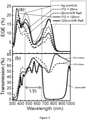
- Figure 3(a) is a graph showing EQE as a function of wavelength for several thicknesses of ITO and control layers with and without NIR reflecting mirrors. The approximate visible photopic range is highlighted by vertical dashed lines.
- Figure 3(b) is a graph showing transmission % as a function of wavelength for several thicknesses of ITO and control layers. Comparing EQE and transmission of the ITO-only devices, the absorption for the thinnest and optimized thicknesses appears equivalent. Inspection of the simulations shows, however, that the NIR field distribution is shifted from within the ITO anode to the ClAlPc active layer as the ITO cathode thickness increases, so that the total transmission appears the same even though the active layer absorption changes substantially. This highlights an important aspect of transparent OPV architectures; despite the seemingly simple optical configuration, interference management is still crucial to device optimization, particularly for NIR absorbing cells and for materials with low exciton diffusion lengths.
- the average visible transmissivity (AVT) shows little variation with ITO thickness (see e.g., Figure 2(a) ).
- the optical model predicts a slight decrease in AVT with ITO thicknesses that is not observed experimentally possibly due to model parameter uncertainties or varying optical constants during thicker ITO growths.
- Optimized cells without the NIR mirror show min (max) transmission values of 50% (74%) at 450nm (540nm) and an AVT of 65% (standard deviation of 7%).
- Figure 3(c) shows the measured solar simulator spectrum (left axis) exhibiting characteristics of the Xe-lamp and NREL reported mc-Si external quantum efficiency (EQE) for the reference-diode used to measure the solar simulator intensity (right-axis). Because the responsivity of the reference diode extends significantly beyond the response of the OPV cell, the extra NIR light from the solar simulator (compared to the AM1.5G spectrum) results in solar mismatch factors less than 1.
- Figure 3(d) shows the measured (left axis, circles) and calculated (left axis, solid line) reflectivity of the distributed Bragg reflector used in this study as the transparent, NIR mirror. Also shown is the transmission spectrum (right-axis) of the broad-band antireflection (BBAR) coatings.
- EQE mc-Si external quantum efficiency
- Figures 4a and 4b show solar cell arrays in front of a picture of a "rose". Both picture-detail and color-clarity are minimally disrupted so that details of the device array pattern are even difficult to discern.
- the array has a common cathode 25a and a plurality of anodes 22a.
- the device also includes an active area 30 which includes the donor layer(s), acceptor layer(s) and reflective mirrors.
- an array of 10 individual OPV devices is formed on the substrate 21a.
- Figure 4(c) shows the array wired to power an LCD clock.
- Figures 4(d) and 4(e) show an alternate embodiment of a solar cell array positioned in front of a picture of a "mountain" to highlight the transparency of the fully assembled device.
- Figure 4(f) is a picture of a full circuit assembly (left). Electrical connections are made to the ITO contacts of the OPV device (array) via carbon-tape.
- the LCD clock is connected to circuitry (right) that limits the voltage and passes excess current to a small LED such that the clock works under a wide range of OPV illumination conditions.
- the LCD clock requires approximately 1.5V and 10 ⁇ A and can be run by the solar cell for intensities ⁇ 0.05 suns (note that under the ambient lighting ⁇ 0.01 sun, the clock is off).
- the optimized power efficiency is nearly triple that of an existing visible-absorbing, semi-transparent, copper phthalocyanine planar device while also exhibiting 30% more average transmission, but is slightly less efficient (0.75x) than semi-transparent bulk-heterojunction structures that gain efficiency from active layer absorption in the visible and subsequently have nearly half the transmission.
- SnPc e.g., SnPc-C 60
- SnPc-C 60 may be used to construct transparent solar cells.
- Solar cell designs based on SnPc may achieve >2% efficient solar cell with >70% transmission of visible light ( ⁇ 70% average transmission across visible spectrum).
- the following layers were used in this example: ITO / SnPc(10nm) / C60(30nm) / BCP(10nm) / ITO(10nm) / DBR.
- the ITO was sputtered directly.
- the distributed Bragg reflectors (DBR) were applied with index matching fluid (IMF).
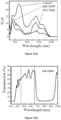
- Figure 5(a) is a graph showing the EQE as a function of wavelength for the SnPc device.
- Figure 5(b) is a graph showing transmissivity as a function of wavelength for the full TOPV SnPc device.
- Table 2 Cathode Jsc Voc FF ⁇ (%) Ag 6.15 0.40 0.55 1.3 ITO 1.54 0.33 0.48 0.2 ITO-DBR 2.25 0.34 0.44 0.3
- the device may include a NIR mirror (transparent to visible light) composed of either metal/oxide (e.g. TiO 2 /Ag/TiO 2 ) or dielectric stacks (DBRs e.g. consisting of SiO 2 /TiO 2 ).
- Anti-reflection coatings may be composed of single or multilayer dielectric materials.
- the molecular active layer may also be composed of any suitable phthalocyanine, porphyrin, naphthalocyanine dye, carbon nanotube, or molecular excitonic materials with absorption peaks outside of the visible spectrum.
- Figure 6(a) is a graph showing a comparison between SnPc and ClAlPc reference (opaque) designs.
- Table 3 Donor Thick Jsc Voc FF n (%) SnPc 100 6.15 0.40 0.50 1.2 ClAlPc 200 4.70 0.77 0.55 2.0
- Figure 6(b) is a graph showing the electric field and the effect of ITO cathode thickness.
- 2 Calculated optical field,
- Figures 6(c) and 6(d) show the transfer matrix simulations of the average visible transmission (AVT, left column) and short-circuit current (right column) of the transparent OPV architecture as a function of the anode and cathode ITO thicknesses without a NIR mirror.
- Figures 6(e) and 6(f) show the transfer matrix simulations of the average visible transmission (AVT, left column) and short-circuit current (right column) of the transparent OPV architecture as a function of the anode and cathode ITO thicknesses with a NIR mirror.
- the vertical dashed line indicates the thickness of the ITO anode utilized in this study.
- the active layer structure was Anode/MoO 3 (20nm) / ClAlPc(15nm) / C 60 (30nm) / BCP(7.5nm) / Cathode where the exciton diffusion lengths of ClAlPc and C 60 were estimated from fitting the magnitudes of the photocurrent and EQE of the control cell to be 8 ⁇ 4nm and 15 ⁇ 6nm, respectively.
- the structure shown in Figure 1(b) includes discrete layers for the donor, e.g., ClAlPc or SnPc, and the acceptor, e.g., C 60 .
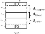
- the donor and acceptor may be combined in a single or mixed layer as shown generally in Figure 7 .
- the device 40 may have a mixed layer 46 including both a donor and an acceptor.
- the mixed layer generally has a thickness d mixed as shown.
- the device 40 may optionally include a discrete donor layer 48 and/or acceptor layer 46.
- the donor layer 48 if present, has a thickness d Donor as shown.
- the acceptor 46 layer if present, has a thickness d Acceptor as shown.
- the device 40 also includes a transparent cathode 42 and a transparent anode 50.
- the thicknesses of each layer may be selected as generally outlined above. It should be understood that such a structure may also include other layers including anti-reflective layers and mirror layers as disclosed in the various embodiments herein.
- An optimization process may generally be performed as follows:
- optimization may include an adjustment of the thickness of the mixed layer (step iii) and an adjustment of the ratio d Donor :d Acceptor (step vi).
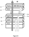
- FIG 8 is a block diagram of a tandem device 60.
- the device 60 generally includes at least a first and second cell 66, 68. Each cell may have the structure generally disclosed above. Each of the first and second cells 66, 68 function has transparent subcells. Each may have a varying NIR spectral responsivity. Each of the first and second cells may have absorption peaks at wavelengths outside of the visible light spectrum.
- a recombination zone 72a is disposed between the first and second cells 66, 68.
- the recombination zone may be composed of a variety of compounds including, e.g., ITO(0.5-10nm), or BCP/Ag(0.1-2nm)/ MoOx.
- the device 60 also includes a cathode 62 and an anode 70.
- the device may optionally include a transparent NIR mirror 62.
- Figures 9(a) and 9(b) are graphs showing different bandgaps associated with materials that may be used to optimize a device, e.g., US J. Aggregate ( Figure 9(a) ) and carbon nanotubes ( Figure 9(b) ).
- multiple bandgaps may be selected for successive layers stacked in a tandem device in order to yield a device with the desired efficiency.
- overall transparency is improved over devices that are independently fabricated and post integrated or macroscopically combined. This is possible because such a device benefits from a closely matched index of refraction at each interface between successive layers.
- the stacked structure may be transparent or semi-transparent.
- Figures 10(a) and 10(b) are graphs showing practical efficiency limits of several of the embodiments disclosed herein.
- Figure 11 is a diagram showing solar flux and the photopic response of the human eye. In general, the photopic response of the human eye peaks in the green spectrum 530-500nm and tapers off below 450nm and above 650nm.
- Figure 12 is a diagram showing an e-reader 80, smart phone 82 and display screen 84 including photovoltaic arrays 86, 88 and 90 disposed on their respective display screens. It should be understood that a variety of devices may incorporate the photovoltaic devices disclosed herein and/or arrays of such devices. Other applications include watch crystals, automotive and architectural glass including sunroofs and privacy glass. The photovoltaic devices may be used for active power generation, e.g., for completely self-powered applications and battery charging (or battery life extension).
Description
- This invention relates to the field of photovoltaic devices and more particularly, organic photovoltaic devices.
- The surface area necessary to take advantage of solar energy remains an obstacle to offsetting a significant portion of non-renewable energy consumption. For this reason, low-cost, transparent, organic photovoltaic (OPV) devices that can be integrated onto window panes in homes, skyscrapers, and automobiles are desirable. For example, window glass utilized in automobiles and architecture are typically 70-80% and 55-90% transmissive, respectively, to the visible spectrum, e.g., light with wavelengths from about 450 to 650 nanometers (nm). The limited mechanical flexibility, high module cost and, more importantly, the band-like absorption of inorganic semiconductors limit their potential utility to transparent solar cells. In contrast, the excitonic character of organic and molecular semiconductors results in absorption spectra that are highly structured with absorption minima and maxima that is uniquely distinct from the band-absorption of their inorganic counterparts. Previous efforts to construct semitransparent devices have focused on the use of thin active layers (or physical holes) with absorption focused in the visible spectrum and therefore have been limited to either low efficiencies < 1% or low average visible transmissivity (AVT) to light around 10-35%, since both parameters cannot be simultaneously optimized.
- The following referenced document discloses a photovoltaic cell. BAILEY-SALZMAN RHONDA ET AL: "Near-infrared sensitive small molecule organic photovoltaic cells based on chloroaluminum phthalocyanine",§ APPLIED PHYSICS LETTERS, AIP, AMERICAN INSTITUTE OF PHYSICS, MELVILLE, NY, US, vol. 91, no. 1, 5 July 2007 (2007-07-05), pages 13508-13508, XP012098993, ISSN: 0003-6951, DOI: 10.1063/1.2752992
- The following referenced document discloses a photovoltaic cell. CHI-FENG LIN , MI ZHANG , SHUN-WEI LIU, TIEN-LUNG CHIU AND JIUN-HAW LEE: "High Photoelectric Conversion Efficiency of Metal Phthalocyanine / Fullerene Heterojunction Photovoltaic Device", INT. J. MOL. SCI., vol. 12, 17 January 2011 (2011-01-17), pages 476-505, XP002675896
- The following referenced document discloses a photovoltaic cell. LI NING ET AL: "Tilted bulk heterojunction organic photovoltaic cells grown by oblique angle deposition", APPLIED PHYSICS LETTERS, AIP, AMERICAN INSTITUTE OF PHYSICS, MELVILLE, NY, US, vol. 95, no. 12, 25 September 2009 (2009-09-25), pages 123309-123309, XP012122205, ISSN: 0003-6951, DOI: 10.1063/1.3236838
- A transparent photovoltaic cell and method of making it in accordance with
claims - The first active material may have a second absorption peak at a wavelength less than about 450 nanometers.
- The first active material may be a donor and the second active material may be an acceptor. The device includes a mirror reflecting at near infra-red wavelengths. The first active material may comprise an organic material. The first active material may comprise at least one of: a phthalocyanine, a porphyrin, or a naphthalocyanine dye. The first active material may comprise chloroaluminum phthalocyanine. The first active layer may comprise tin phthalocyanine. The second active layer may comprise at least one of carbon 60 (C60) or a nanotube. The first and second active materials may be configured for use with flexible encapsulation layers.
- The photovoltaic cell may include a recombination zone disposed between a first and second subcell, each of the first and second subcells having absorption peaks at wavelengths outside of the visible light spectrum, a transparent cathode and a transparent anode.
-
-
Figure 1(a) shows a schematic of a control solar cell; -
Figure 1(b) shows a schematic of a full transparent solar cell embodiment; -
Figure 1(c) is a graph showing the extinction coefficient, k, of the active layers shown inFigures 1(a) and 1(b) ; -
Figure 1(d) is a graph showing the current-voltage (J-V) curves for the ClAlPc-C60 control and transparent cells shown inFigures 1(a) and 1(b) ; -
Figure 2(a) is a graph showing the series resistance diminish and the fill factor (FF) saturates close to the value for the control cell as Indium Tin Oxide (ITO) thickness is increased; -
Figure 2(b) is a graph showing photocurrent increase by a factor of 3x at an optimum thickness of 120nm so that ηp increases by nearly the same amount; -
Figure 3(a) is a graph showing external quantum efficiency (EQE) as a function of wavelength for several thicknesses of ITO and control layers; -
Figure 3(b) is a graph showing transmission % as a function of wavelength for several thicknesses of ITO and control layers; -
Figure 3(c) shows the measured solar simulator spectrum exhibiting characteristics of the Xe-lamp and NREL reported mc-Si external quantum efficiency (EQE) for the reference-diode used to measure the solar simulator intensity; -
Figure 3(d) shows the measured and calculated reflectivity of the distributed Bragg reflector used in this study as the transparent, NIR mirror; -
Figures 4a and 4b show solar cell arrays positioned in front of a picture of a "rose" to highlight the transparency of the fully assembled device; -
Figure 4c shows a solar cell array coupled to an LCD clock; -
Figures 4d and 4e show an alternate embodiment of a solar cell array positioned in front of a picture of a "mountain" to highlight the transparency of the fully assembled device; -
Figure 4(f) is a picture of a full circuit assembly with connections to an LCD clock. -
Figure 5(a) is a graph showing external quantum efficiency (EQE) as a function of wavelength for a SnPc device; -
Figure 5(b) is a graph showing transmission % as a function of wavelength for a SnPc device; -
Figure 6(a) is a graph showing a comparison between SnPc and ClAlPc designs; -
Figure 6(b) is a graph showing the effect of ITO cathode thickness; -
Figure 6(c) and 6(d) show the transfer matrix simulations of the average visible transmission (AVT, left column) and short-circuit current (right column) of the transparent OPV architecture as a function of the anode and cathode ITO thicknesses without a NIR mirror; -
Figure 6(e) and 6(f) show the transfer matrix simulations of the average visible transmission (AVT, left column) and short-circuit current (right column) of the transparent OPV architecture as a function of the anode and cathode ITO thicknesses with a NIR mirror; -
Figure 7 is a block diagram of a device with a mixed layer including both a donor and an acceptor; -
Figure 8 is a block diagram of a tandem device; -
Figures 9(a) and 9(b) are graphs showing different bandgaps that may be used to optimize a tandem device; -
Figures 10(a) and 10(b) are graphs showing practical efficiency limits of several of the embodiments disclosed herein; -
Figure 11 is a diagram showing the solar flux and the photopic response of the human eye; and -
Figure 12 is a diagram showing an e-reader, smart phone and display screen including a photovoltaic array as disclosed herein. - Described herein are improved transparent solar cell designs, e.g., transparent organic photovoltaic devices (TOPV). The term transparent as used herein encompasses an average visible transparency of a straight through beam of 45% or more. The term semi-transparent as used herein encompasses an average visible transparency of a straight through beam of approximately 10%-45%. In general, the designs include molecular active layers with strong absorption features outside of the visible light spectrum, e.g., in the ultra-violet (UV) and/or near-infrared (NIR) solar spectrum. The devices may include selective high-reflectivity NIR and broadband anti-reflection contact coatings. Devices may be formed as heterojunction solar cells with an organic active layer, such as chloroaluminum phthalocyanine (ClAlPc) or SnPc as a donor and a molecular active layer such as C60 acting as an acceptor and having peak-absorption in the UV and NIR solar spectrum. Other suitable materials for the active layers include any suitable phthalocyanine, porphyrin, naphthalocynanine dye, carbon nanotubes or molecular excitonic materials with absorption peaks outside the visible spectrum. Such devices may be formed in a tandem structure with one or more subcells joined via a recombination zone. Such devices may be used in a variety of applications including rigid and flexible computer display screens used in a desktop monitor, laptop or notebook computer, tablet computer, mobile phone, e-readers and the like. Other applications include watch crystals, automotive and architectural glass including sunroofs and privacy glass. The photovoltaic devices may be used for active power generation, e.g., for completely self-powered applications, and battery charging (or battery life extension).
- Near-infrared (NIR) as recited herein is defined as light having wavelengths in the range from about 650 to about 850 nanometers (nm). Ultraviolet (UV) as recited herein is defined as light having wavelengths less than about 450 nm. The use of an active layer having absorption in the NIR and the UV allows for the use of selective high-reflectivity near-infrared mirror coatings to optimize device performance while also permitting high transmission of visible light through the entire device. Visible light as recited herein is defined as light having wavelengths to which the human eye has a significant response, from about 450 to about 650 nm.
- In one embodiment, devices were fabricated on 150nm of patterned Indium Tin Oxide (ITO) (15 Ω/sq.) pre-coated onto glass substrates. The ITO is one component of an electrode. The ITO was solvent-cleaned and subsequently treated in oxygen plasma for 30 seconds immediately prior to loading into a high vacuum chamber (<1×10⁻⁶ Torr, wherein 1 Torr is equal to 133,32 Pa) . ClAlPc and C60 were purified once by vacuum train sublimation prior to loading. Bathocuproine (BCP) and molybdenum trioxide (MoO3) were used as purchased. MoO3 is another component of an electrode. The MoO3 (20nm), ClAlPc (15nm), C60 (30nm), BCP (7.5nm), and a 100nm thick Ag cathode were sequentially deposited via thermal evaporation at a rate of 0.1nm/s. The top ITO cathode for the transparent devices was rf-sputtered directly onto the organic layers at low power (7-25W) with 10 sccm Ar flow (6 mTorr) and 0.005-0.03nm/second. Cathodes were evaporated through a shadow mask, defining a 1 millimeter (mm) x 1.2 mm active device area. A near-infrared distributed Bragg reflector (DBR) utilized as the transparent NIR mirror was grown separately on quartz via sputtering of 7 alternating layers of TiO2 and SiO2 at about 0.1nm/second with thicknesses centered around a wavelength of 800nm (200nm stop band). Broad-band antireflection (BBAR) coatings precoated on quartz substrates (1-side) were attached to the DBRs via index matching fluid to reduce additional glass/air interface reflections. Transmission data of the assembled devices were obtained at normal incidence with a Cary Eclipse 5000 dual-beam spectrophotometer without reference samples. Current density versus voltage (J-V) characteristics were measured in the dark and under simulated AM1.5G solar illumination without solar mismatch correction (for reference, the mismatch factor was estimated to be ~1.05) and external quantum efficiency (EQE) measurements were collected utilizing an NREL calibrated Si detector. Optical interference modeling was carried out according to the method of L. A. A. Pettersson, L. S. Roman, and O. Inganas, Journal of Applied Physics 86, 487 (1999). The exciton diffusion lengths of ClAlPc and C60 were estimated from fitting the magnitudes of the photocurrent and EQE to be 5 ± 3nm and 10 ± 5nm, respectively.
-
Figure 1(a) shows a schematic of a controlsolar cell 10. The control solar cell includes asubstrate 11, ananode 12, adonor layer 13 e.g., ClAlPc, a molecular active layer, e.g., C60, acting as anacceptor layer 14 and acathode 15. In this example, theanode 15 is opaque, e.g., silver.Figure 1(b) shows a schematic of a full transparentsolar cell 20. Thedevice 20 generally includes atransparent substrate 21, ananode 22, adonor layer 23, e.g., ClAlPc, a molecular active layer, e.g., C60, acting as anacceptor layer 24, and acathode 25. Thedonor layer 23 and theacceptor layer 24 have absorption peaks in the ultra-violet (UV) and near-infrared (NIR) spectrum. In this example, the substrate is quartz. It should be understood that a variety of rigid and flexible substrates may be used. For example, the substrate may be glass, a rigid or flexible polymer, e.g., a screen protector or skin, or may be combined with other layers such as encapsulating layers, anti-reflecting layers or the like. In this example, thetransparent anode 22 andcathode 25 are formed of conducting oxide, e.g. ITO/MoO3. It should be understood that theanode 22 andcathode 25 may be formed of other materials such as tin oxides, fluorinated tin oxides, nanotubes, Poly(3,4-ethylenedioxythiophene) (PDOT) or PEDOT:PSS (Poly(3,4-ethylenedioxythiophene) poly(styrenesulfonate)), gallium doped zinc oxide, aluminum doped zinc oxide and other materials having suitable transparency and conductivity. Thedevice 20 may also include a near-infrared DBR 26 and one or more broad-band antireflection (BBAR)coatings 27. -
Figure 1(c) is a graph showing the extinction coefficient, k, of the active layers shown inFigures 1(a) and 1(b). Figure 1(d) is a graph showing the current-voltage (J-V) curves for the ClAlPc-C60 control and transparent cells ofFigures 1(a) and 1(b) for a range of thicknesses of ITO. The absorption peak for ClAlPc is positioned in the NIR range (~740nm). This allows for the incorporation of a NIR reflecting mirror and simultaneous optimization of the solar cell performance and visible-transmissivity as diagramed inFigures 1(a) and 1(b) . It should be understood that the donor and/or acceptor layers may have one or more absorption peaks outside of the visual spectrum. In this example, the ClAlPc also has a second absorption peak in the UV range. A summary of various device performances is provided in Table 1.Table 1 Cathode Thickness (nm) Cathode Composition Jsc (mA/cm2) Voc (V) FF - Jsc (%) AVT (%) 100 Ag 4.7 0.77 0.55 2.4 0 20 ITO 1.5 0.69 0.39 0.5 67 120 ITO 3.2 0.71 0.46 1.3 65 20 ITO/NIR mir. 2.2 0.73 0.32 0.6 53 40 ITO/NIR mir. 2.5 0.71 0.49 1.1 55 80 ITO/NIR mir. 2.9 0.71 0.46 1.2 56 120 ITO/NIR mir. 4.4 0.71 0.44 1.7 56 170 ITO/NIR mir. 3.2 0.69 0.48 1.3 66 - Table 1 generally includes data showing the performance of control OPVs with an Ag cathode, transparent OPVs with ITO cathode, and OPVs with ITO cathode and NIR mirror, at 0.8 sun illumination corrected for solar spectrum mismatch. Short circuit current, JSC, open circuit voltage, VOC, fill factor, FF, power conversion efficiency, η P, and the average visible transmission, AVT, are indicated. The control device with a thick Ag cathode exhibits a power conversion efficiency (ηp ) of 1.9±0.2%, open circuit voltage (Voc) = 0.80±0.02V, short-circuit current density (Jsc) = 4.7±0.3mA/cm2, and fill-factor (FF) = 0.55±0.03, which is comparable to previous reports.
- When the Ag cathode of the control cell is replaced with ITO, the short-circuit current Jsc drops significantly to 1.5±0.1mA/cm2, the FF drops to 0.35±0.02, and the open-circuit voltage Voc decreases slightly to 0.7±0.02V leading to ηp = 0.4±0.1%. The FF decreases due to an increase in series resistance from the thin ITO that is observable in the J-V curve under forward bias in
Figure 1(c) .Figure 2(a) is a graph showing the series resistance diminish and the FF saturate close to the value for the control cell as ITO thickness is increased. InFigures 2(a) and 2(b) , the solid lines are from actual simulations, the dashed lines are simply guides to the eye. The slight drop in Voc, independent of ITO thickness, is likely due to a slight reduction in the cathode-anode work function offset. Nonetheless it is remarkable that when utilizing ITO as both anode and cathode there is enough deposition anisotropy in the work function to support this large Voc and is likely assisted by the large work function MoO3 layer. - The Jsc decreases as the cathode is switched from Ag to ITO due to reduced cathode reflections that reduce the total absorption across the spectrum in the active layers.
Figure 2(b) is a graph showing photocurrent increase by a factor of 3x at an optimum thickness of 120nm so that ηp increases by nearly the same amount. Fitting this data with the optical interference model shows that this behavior stems from interference of the backside ITO cathode reflection.Figure 3(a) is a graph showing EQE as a function of wavelength for several thicknesses of ITO and control layers with and without NIR reflecting mirrors. The approximate visible photopic range is highlighted by vertical dashed lines.Figure 3(b) is a graph showing transmission % as a function of wavelength for several thicknesses of ITO and control layers. Comparing EQE and transmission of the ITO-only devices, the absorption for the thinnest and optimized thicknesses appears equivalent. Inspection of the simulations shows, however, that the NIR field distribution is shifted from within the ITO anode to the ClAlPc active layer as the ITO cathode thickness increases, so that the total transmission appears the same even though the active layer absorption changes substantially. This highlights an important aspect of transparent OPV architectures; despite the seemingly simple optical configuration, interference management is still crucial to device optimization, particularly for NIR absorbing cells and for materials with low exciton diffusion lengths. - Despite the significant impact on the photocurrent, the average visible transmissivity (AVT) shows little variation with ITO thickness (see e.g.,
Figure 2(a) ). The optical model predicts a slight decrease in AVT with ITO thicknesses that is not observed experimentally possibly due to model parameter uncertainties or varying optical constants during thicker ITO growths. Optimized cells without the NIR mirror show min (max) transmission values of 50% (74%) at 450nm (540nm) and an AVT of 65% (standard deviation of 7%). These transmission values decrease slightly with the incorporation of the NIR reflector to min (max) transmission values of 47% (68%) at 450nm (560nm) and an AVT of 56% (standard deviation of 5%), where this reduction results from increased off-resonance visible reflections of the mirror. It is possible to remove the off-resonance reflection oscillations in the visible spectra by designing more complex hot-mirror architectures to improve the AVT closer to that of the cell without the NIR mirror, but this typically requires a greater number layers. Hot mirror architectures are described in A. Thelen, Thin Films for Optical Systems 1782, 2 (1993). High reflectivity of 99% between 695-910 nm also makes these devices useful for simultaneous NIR rejection in architectural cooling. Additionally, the use of the BBAR coatings next to the DBR (outcoupling) and below the substrates (incoupling), results in a concomitant increase in the quantum efficiency by ~2-3% and the AVT by ~4-6%. -
Figure 3(c) shows the measured solar simulator spectrum (left axis) exhibiting characteristics of the Xe-lamp and NREL reported mc-Si external quantum efficiency (EQE) for the reference-diode used to measure the solar simulator intensity (right-axis). Because the responsivity of the reference diode extends significantly beyond the response of the OPV cell, the extra NIR light from the solar simulator (compared to the AM1.5G spectrum) results in solar mismatch factors less than 1.Figure 3(d) shows the measured (left axis, circles) and calculated (left axis, solid line) reflectivity of the distributed Bragg reflector used in this study as the transparent, NIR mirror. Also shown is the transmission spectrum (right-axis) of the broad-band antireflection (BBAR) coatings. - To highlight the transparency of the fully assembled device,
Figures 4a and 4b show solar cell arrays in front of a picture of a "rose". Both picture-detail and color-clarity are minimally disrupted so that details of the device array pattern are even difficult to discern. In this example the array has acommon cathode 25a and a plurality ofanodes 22a. The device also includes anactive area 30 which includes the donor layer(s), acceptor layer(s) and reflective mirrors. In this particular example, an array of 10 individual OPV devices is formed on thesubstrate 21a.Figure 4(c) shows the array wired to power an LCD clock.Figures 4(d) and 4(e) show an alternate embodiment of a solar cell array positioned in front of a picture of a "mountain" to highlight the transparency of the fully assembled device. -
Figure 4(f) is a picture of a full circuit assembly (left). Electrical connections are made to the ITO contacts of the OPV device (array) via carbon-tape. The LCD clock is connected to circuitry (right) that limits the voltage and passes excess current to a small LED such that the clock works under a wide range of OPV illumination conditions. The LCD clock requires approximately 1.5V and 10µA and can be run by the solar cell for intensities ≥ 0.05 suns (note that under the ambient lighting < 0.01 sun, the clock is off). - Optimizing the transparent OPV structure with just the cathode thickness, power conversion efficiency of 1.0±0.1% is obtained, with a simultaneous average transmission of 66±3%. Incorporation of the NIR reflector and BBAR coatings with the optimized ITO thickness (see
Figure 2(a) ) improves the power conversion efficiency to 1.4±0.1% with an average transmission of 56±2%. With the NIR mirror, the increase in power conversion efficiency stems from additional NIR photocurrent in the ClAlPc layer where the EQE shows a near doubling of the peak ClAlPc EQE from 10% to 18% (seeFigure 3(a) ). The optimized power efficiency is nearly triple that of an existing visible-absorbing, semi-transparent, copper phthalocyanine planar device while also exhibiting 30% more average transmission, but is slightly less efficient (0.75x) than semi-transparent bulk-heterojunction structures that gain efficiency from active layer absorption in the visible and subsequently have nearly half the transmission. - Switching from planar to bulk-heterojunctions in these structures, efficiencies of 2-3% may be possible for this material set with nearly identical visible transmission, and is currently under investigation. Tandem stacking of subcells with active layer absorption deeper into the infrared could also enhance these efficiencies; combined with more sophisticated NIR mirrors, efficiencies beyond several percent and average visible transmission >70% are possible.
- In another embodiment, SnPc, e.g., SnPc-C60, may be used to construct transparent solar cells. Solar cell designs based on SnPc may achieve >2% efficient solar cell with >70% transmission of visible light (~70% average transmission across visible spectrum). The following layers were used in this example: ITO / SnPc(10nm) / C60(30nm) / BCP(10nm) / ITO(10nm) / DBR. In this example, the ITO was sputtered directly. The distributed Bragg reflectors (DBR) were applied with index matching fluid (IMF).
Figure 5(a) is a graph showing the EQE as a function of wavelength for the SnPc device.Figure 5(b) is a graph showing transmissivity as a function of wavelength for the full TOPV SnPc device. A summary of various device performances is provided in Table 2:Table 2 Cathode Jsc Voc FF η (%) Ag 6.15 0.40 0.55 1.3 ITO 1.54 0.33 0.48 0.2 ITO-DBR 2.25 0.34 0.44 0.3 - The device may include a NIR mirror (transparent to visible light) composed of either metal/oxide (e.g. TiO2/Ag/TiO2) or dielectric stacks (DBRs e.g. consisting of SiO2/TiO2). Anti-reflection coatings may be composed of single or multilayer dielectric materials. As noted above, the molecular active layer may also be composed of any suitable phthalocyanine, porphyrin, naphthalocyanine dye, carbon nanotube, or molecular excitonic materials with absorption peaks outside of the visible spectrum.
-
Figure 6(a) is a graph showing a comparison between SnPc and ClAlPc reference (opaque) designs. A summary of various device performances is provided in Table 3:Table 3 Donor Thick Jsc Voc FF n (%) SnPc 100 6.15 0.40 0.50 1.2 ClAlPc 200 4.70 0.77 0.55 2.0 -
Figure 6(b) is a graph showing the electric field and the effect of ITO cathode thickness. Calculated optical field, |E|2, of the transparent OVP as a function of position at a fixed wavelength close to the peak absorption of the ClAlPc active layer (~740nm) for an ITO cathode thickness of 20nm (black line) and 120nm (red line). Note the enhancement of the field within the ClAlPc layer for the optimized ITO thickness, where the absorption is proportional to |E|2 integrated over position. In general, there is a strong dependence on ITO thickness. -
Figures 6(c) and 6(d) show the transfer matrix simulations of the average visible transmission (AVT, left column) and short-circuit current (right column) of the transparent OPV architecture as a function of the anode and cathode ITO thicknesses without a NIR mirror.Figures 6(e) and 6(f) show the transfer matrix simulations of the average visible transmission (AVT, left column) and short-circuit current (right column) of the transparent OPV architecture as a function of the anode and cathode ITO thicknesses with a NIR mirror. The vertical dashed line indicates the thickness of the ITO anode utilized in this study. The active layer structure was Anode/MoO3(20nm) / ClAlPc(15nm) / C60(30nm) / BCP(7.5nm) / Cathode where the exciton diffusion lengths of ClAlPc and C60 were estimated from fitting the magnitudes of the photocurrent and EQE of the control cell to be 8±4nm and 15±6nm, respectively. - The structure shown in
Figure 1(b) includes discrete layers for the donor, e.g., ClAlPc or SnPc, and the acceptor, e.g., C60. It should be understood that the donor and acceptor may be combined in a single or mixed layer as shown generally inFigure 7 . In this embodiment thedevice 40 may have amixed layer 46 including both a donor and an acceptor. The mixed layer generally has a thickness dmixed as shown. Thedevice 40 may optionally include adiscrete donor layer 48 and/oracceptor layer 46. Thedonor layer 48, if present, has a thickness dDonor as shown. Theacceptor 46 layer, if present, has a thickness dAcceptor as shown. It should be understood thatFigure 7 is simplified for matters of clarity and may include additional layers that are not shown. In this example, thedevice 40 also includes atransparent cathode 42 and atransparent anode 50. The thicknesses of each layer may be selected as generally outlined above. It should be understood that such a structure may also include other layers including anti-reflective layers and mirror layers as disclosed in the various embodiments herein. - An optimization process may generally be performed as follows:
- i) Optimize for dDonor, dAcceptor (total);
- ii) Fix dDonor, dAcceptor (total);
- iii) Vary dmixed;
- iv)

- v)

- vi) Optimize for ratio (dDonor:dAcceptor).
- For devices having a mixed layer only, optimization may include an adjustment of the thickness of the mixed layer (step iii) and an adjustment of the ratio dDonor:dAcceptor (step vi).
-
Figure 8 is a block diagram of atandem device 60. Thedevice 60 generally includes at least a first andsecond cell second cells recombination zone 72a is disposed between the first andsecond cells reference number 72b. It should be understood thatFigure 8 is simplified for matters of clarity and may include additional layers that are not shown. In this example, thedevice 60 also includes acathode 62 and ananode 70. The device may optionally include atransparent NIR mirror 62.Figures 9(a) and 9(b) are graphs showing different bandgaps associated with materials that may be used to optimize a device, e.g., US J. Aggregate (Figure 9(a) ) and carbon nanotubes (Figure 9(b) ). - It should be understood that multiple bandgaps may be selected for successive layers stacked in a tandem device in order to yield a device with the desired efficiency. In such devices, overall transparency is improved over devices that are independently fabricated and post integrated or macroscopically combined. This is possible because such a device benefits from a closely matched index of refraction at each interface between successive layers. The stacked structure may be transparent or semi-transparent.
-
Figures 10(a) and 10(b) are graphs showing practical efficiency limits of several of the embodiments disclosed herein.Figure 11 is a diagram showing solar flux and the photopic response of the human eye. In general, the photopic response of the human eye peaks in the green spectrum 530-500nm and tapers off below 450nm and above 650nm. -
Figure 12 is a diagram showing ane-reader 80, smart phone 82 and display screen 84 includingphotovoltaic arrays 86, 88 and 90 disposed on their respective display screens. It should be understood that a variety of devices may incorporate the photovoltaic devices disclosed herein and/or arrays of such devices. Other applications include watch crystals, automotive and architectural glass including sunroofs and privacy glass. The photovoltaic devices may be used for active power generation, e.g., for completely self-powered applications and battery charging (or battery life extension). - In conclusion, near-infrared absorbing, transparent planar organic solar cells with a maximum power of 1.4±0.1% and average visible transmission of exceeding 55±2% have been demonstrated. This average visible transmission is sufficiently transparent for incorporation on architectural glass. The excitonic character of organic semiconductors is advantageously exploited to produce unique photovoltaic architectures not easily accessible via inorganic semiconductors. By positioning the active layer absorption selectively in the NIR, it is possible to optimize the architecture using a NIR reflector composed of a DBR mirror centered at 800nm that results in a transparent solar cell efficiency approaching that of the non-transparent control cell. Ultimately these devices provide a guide for achieving high efficiency and high transparency solar cells that can be utilized in windows to generate power, reduce cooling costs, and scavenge energy in a variety of applications.
Claims (12)
- A transparent photovoltaic cell (20), comprising:a transparent substrate (21);a transparent anode (22) overlying the transparent substrate (21);
a first transparent active material (23) overlying the transparent anode (22), the first transparent active material (23) having an absorption peak at a wavelength greater than 650 nanometers;a second transparent active material (24) overlying the transparent anode (22), the second transparent active material (24) having an absorption peak at a wavelength outside of the visible light spectrum;a transparent cathode (25) overlying the transparent substrate (21), the transparent anode (22), and the first and second transparent active materials (23, 24); wherein the first transparent active material and the second transparent active material are positioned between the transparent anode and the transparent cathode; anda visibly transparent multi-layer mirror (62) overlying the cathode (25), configured to reflect at near infra-red wavelengths;wherein transparent is an average visible transparency of a straight through beam of 45% or more. - The transparent photovoltaic cell of claim 1, wherein the first transparent active material (23) has a second absorption peak at a wavelength less than 450 nanometers.
- The transparent photovoltaic cell of claim 1, wherein the first transparent active material (23) is a donor and the second transparent active material (24) is an acceptor.
- The transparent photovoltaic cell of claim 1, wherein the first transparent active material comprises an organic material.
- The transparent photovoltaic cell of claim 1, wherein the first transparent active material comprises at least one of: a phthalocyanine, a porphyrin, or a naphthalocyanine dye.
- The transparent photovoltaic cell of claim 1, wherein the first transparent active material comprises chloroaluminum phthalocyanine.
- The transparent photovoltaic cell of claim 1, wherein the first transparent active layer (23) comprises tin phthalocyanine.
- The transparent photovoltaic cell of claim 1, wherein the second transparent active layer (24) comprises at least one of carbon 60 (060) or a nanotube.
- The transparent photovoltaic cell of claim 1, wherein the photovoltaic cell (20) is incorporated into one of a display screen, a watch crystal, automotive glass or architectural glass.
- A transparent photovoltaic array comprising a plurality of electrically interconnected photovoltaic cells according to claim 1.
- The transparent photovoltaic cell of claim 1, wherein the transparent substrate is flexible.
- A method of generating electricity, the method comprising:providing a transparent photovoltaic cell (20) comprising:a transparent substrate (21);
a transparent anode (22) overlying the transparent substrate (21);a first transparent active material (23) overlying the transparent anode (22), the first transparent active material (23) having an absorption peak at a wavelength greater than 650 nanometers;a second transparent active material (24) overlying the transparent anode (22), the second transparent active material (24) having an absorption peak at a wavelength outside of the visible light spectrum;a transparent cathode (25) overlying the transparent substrate (21), the transparent anode (22), and the first and second transparent active materials (23, 24);wherein the first transparent active material and the second transparent active material are positioned between the transparent anode and the transparent cathode; anda visibly transparent multi-layer mirror (62) overlying the cathode, configured to reflect at near infra-red wavelengths; andexposing the photovoltaic cell (20) to a light source; wherein transparent is an average visible transparency of a straight through beam of 45% or more.
Priority Applications (2)
| Application Number | Priority Date | Filing Date | Title |
|---|---|---|---|
| EP21216267.1A EP4007003A1 (en) | 2011-01-26 | 2012-01-25 | Transparent photovoltaic cells |
| PL12701431T PL2668680T3 (en) | 2011-01-26 | 2012-01-25 | Transparent photovoltaic cells |
Applications Claiming Priority (2)
| Application Number | Priority Date | Filing Date | Title |
|---|---|---|---|
| US201161436371P | 2011-01-26 | 2011-01-26 | |
| PCT/US2012/022543 WO2012103212A2 (en) | 2011-01-26 | 2012-01-25 | Transparent photovoltaic cells |
Related Child Applications (1)
| Application Number | Title | Priority Date | Filing Date |
|---|---|---|---|
| EP21216267.1A Division EP4007003A1 (en) | 2011-01-26 | 2012-01-25 | Transparent photovoltaic cells |
Publications (2)
| Publication Number | Publication Date |
|---|---|
| EP2668680A2 EP2668680A2 (en) | 2013-12-04 |
| EP2668680B1 true EP2668680B1 (en) | 2022-01-19 |
Family
ID=45541129
Family Applications (2)
| Application Number | Title | Priority Date | Filing Date |
|---|---|---|---|
| EP21216267.1A Pending EP4007003A1 (en) | 2011-01-26 | 2012-01-25 | Transparent photovoltaic cells |
| EP12701431.4A Active EP2668680B1 (en) | 2011-01-26 | 2012-01-25 | Transparent photovoltaic cells |
Family Applications Before (1)
| Application Number | Title | Priority Date | Filing Date |
|---|---|---|---|
| EP21216267.1A Pending EP4007003A1 (en) | 2011-01-26 | 2012-01-25 | Transparent photovoltaic cells |
Country Status (14)
| Country | Link |
|---|---|
| US (4) | US9728735B2 (en) |
| EP (2) | EP4007003A1 (en) |
| JP (4) | JP2014505370A (en) |
| KR (3) | KR20140021542A (en) |
| CN (2) | CN109244247B (en) |
| AU (1) | AU2012209126B2 (en) |
| BR (1) | BR112013019158B1 (en) |
| CA (1) | CA2825584C (en) |
| DK (1) | DK2668680T3 (en) |
| ES (1) | ES2907221T3 (en) |
| MX (1) | MX339751B (en) |
| PL (1) | PL2668680T3 (en) |
| RU (1) | RU2593915C2 (en) |
| WO (1) | WO2012103212A2 (en) |
Families Citing this family (47)
| Publication number | Priority date | Publication date | Assignee | Title |
|---|---|---|---|---|
| DK2668680T3 (en) | 2011-01-26 | 2022-03-21 | Massachusetts Inst Technology | TRANSPARENT PHOTOVOLTAIC CELLS |
| US20130063493A1 (en) * | 2011-09-14 | 2013-03-14 | Htc Corporation | Devices and Methods Involving Display Interaction Using Photovoltaic Arrays |
| US20150122324A1 (en) * | 2012-05-18 | 2015-05-07 | Brookhaven Science Associates, Llc | Thin-film photovoltaic device with optical field confinement and method for making same |
| CN108470776B (en) * | 2012-10-01 | 2022-07-29 | 无处不在能量公司 | Wavelength selective optoelectronic device for a display or a device having a display |
| US10510914B2 (en) | 2013-03-21 | 2019-12-17 | Board Of Trustees Of Michigan State University | Transparent energy-harvesting devices |
| EP2800161B1 (en) * | 2013-04-30 | 2020-01-22 | Fundació Institut de Ciències Fotòniques | Semitransparent photoconversion device |
| EP2838095A1 (en) | 2013-08-15 | 2015-02-18 | CSEM Centre Suisse d'Electronique et de Microtechnique SA - Recherche et Développement | Light harvesting photovoltaic device |
| US9876184B2 (en) * | 2013-08-28 | 2018-01-23 | Taiwan Semiconductor Manufacturing Company, Ltd. | Organic photosensitive device with an electron-blocking and hole-transport layer |
| CN103531712B (en) * | 2013-10-27 | 2016-03-16 | 中国乐凯集团有限公司 | A kind of organic solar batteries |
| EP3161955A4 (en) | 2014-06-27 | 2018-03-28 | The Administrators Of The Tulane Educational Fund | Infrared transmissive concentrated photovoltaics for coupling solar electric energy conversion to solar thermal energy utilization |
| US10941612B2 (en) * | 2015-02-24 | 2021-03-09 | Lutron Technology Company Llc | Photovoltaic cells arranged in a pattern |
| DE112016001262T5 (en) * | 2015-03-18 | 2017-12-28 | Sumitomo Chemical Company, Limited | Photoelectric conversion apparatus comprising a reflection plate |
| JP7131910B2 (en) | 2015-04-27 | 2022-09-06 | ボード オブ トラスティーズ オブ ミシガン ステート ユニバーシティ | Photoactive device and manufacturing method thereof |
| US10163165B1 (en) | 2015-08-11 | 2018-12-25 | State Farm Mutual Automobile Insurance Company | Systems and methods for impact resistant and photovoltaic windows |
| US11489483B2 (en) | 2015-12-09 | 2022-11-01 | Brian Patrick Janowski | Solar window construction and methods |
| US11909352B2 (en) | 2016-03-28 | 2024-02-20 | The Administrators Of The Tulane Educational Fund | Transmissive concentrated photovoltaic module with cooling system |
| KR20230020578A (en) | 2017-01-10 | 2023-02-10 | 유비쿼터스 에너지 인코포레이티드 | Window-integrated transparent photovoltaic module |
| US10651334B2 (en) | 2017-02-14 | 2020-05-12 | International Business Machines Corporation | Semitransparent chalcogen solar cell |
| US10457148B2 (en) | 2017-02-24 | 2019-10-29 | Epic Battery Inc. | Solar car |
| WO2018157089A1 (en) * | 2017-02-24 | 2018-08-30 | The Administrators Of The Tulane Educational Fund | Concentrated solar photovoltaic and photothermal system |
| JP2018161044A (en) * | 2017-03-22 | 2018-10-11 | 住友化学株式会社 | Solar power system |
| CN106876594A (en) * | 2017-03-31 | 2017-06-20 | 华南理工大学 | A kind of translucent solar cell device and application |
| WO2018187384A1 (en) | 2017-04-03 | 2018-10-11 | Epic Battery Inc. | Modular solar battery |
| EP3635793A4 (en) | 2017-05-09 | 2021-01-20 | Ubiqd Inc. | Luminescent optical elements for agricultural applications |
| US11545635B2 (en) | 2017-06-16 | 2023-01-03 | Ubiquitous Energy, Inc. | Visibly transparent, near-infrared-absorbing boron-containing photovoltaic devices |
| US11152581B2 (en) | 2017-06-16 | 2021-10-19 | Ubiquitous Energy, Inc. | Visibly transparent, near-infrared-absorbing donor/acceptor photovoltaic devices |
| US11778896B2 (en) | 2017-06-16 | 2023-10-03 | Ubiquitous Energy, Inc. | Visibly transparent, near-infrared-absorbing metal-complex photovoltaic devices |
| US10903438B2 (en) | 2017-06-16 | 2021-01-26 | Ubiquitous Energy, Inc. | Visibly transparent, ultraviolet-absorbing photovoltaic devices |
| CN110944986A (en) * | 2017-06-16 | 2020-03-31 | 无处不在能量公司 | Visible transparent near-infrared and ultraviolet absorbing photovoltaic devices |
| US10992252B2 (en) | 2017-12-19 | 2021-04-27 | Universal Display Corporation | Integrated photovoltaic window and light source |
| US10613035B2 (en) * | 2018-01-17 | 2020-04-07 | Chromera, Inc. | Optically determining the condition of goods |
| US11061226B2 (en) | 2018-02-19 | 2021-07-13 | Honda Motor Co., Ltd. | Control of electrochromic pixels using integrated transparent photovoltaic converters and projected light for a transparent window display |
| CN113016078A (en) * | 2018-09-14 | 2021-06-22 | 无处不在能量公司 | Method and system for a multilayer transparent electrode for a transparent photovoltaic device |
| US10926223B2 (en) * | 2019-04-11 | 2021-02-23 | Imam Abdulrahman Bin Faisal University | Apparatus for solar-assisted water distillation using waste heat of air conditioners |
| CN114144885A (en) * | 2019-05-29 | 2022-03-04 | 北卡罗莱纳州立大学 | Heat-insulating transparent laminated organic solar cell |
| US11343257B2 (en) * | 2019-06-27 | 2022-05-24 | Microsoft Technology Licensing, Llc | Extended domain platform for nonmember user account management |
| US11489082B2 (en) | 2019-07-30 | 2022-11-01 | Epic Battery Inc. | Durable solar panels |
| WO2021034714A1 (en) * | 2019-08-16 | 2021-02-25 | Ubiquitous Energy, Inc. | Method and system for color neutral transparent photovoltaics |
| CN114930541A (en) | 2019-08-16 | 2022-08-19 | 无处不在能量公司 | Para-phenylene materials as buffer and color adjustment layers for solar cells |
| RU196426U1 (en) * | 2019-12-27 | 2020-02-28 | федеральное государственное автономное образовательное учреждение высшего образования "Национальный исследовательский университет ИТМО" (Университет ИТМО) | Oxide transparent heterojunction |
| KR20210133493A (en) * | 2020-04-29 | 2021-11-08 | 삼성전자주식회사 | Sensor and electronic device |
| US20210359237A1 (en) * | 2020-05-15 | 2021-11-18 | Ubiquitous Energy, Inc. | Solar heat gain coefficient improvement by incorporating nir absorbers |
| NL2027206B1 (en) | 2020-12-22 | 2023-05-03 | Stichting Duurzame Energie Texel | Method of operating a solar energy system and solar energy system |
| CN112928216B (en) * | 2021-02-03 | 2023-08-22 | 西湖大学 | Preparation method of high-transparency solar cell |
| CN113258004A (en) * | 2021-04-16 | 2021-08-13 | 杭州电子科技大学 | Semitransparent solar cell based on distributed Bragg reflector and preparation method thereof |
| CN115707260A (en) * | 2021-08-04 | 2023-02-17 | 隆基绿能科技股份有限公司 | Perovskite battery and photovoltaic module |
| WO2023128039A1 (en) * | 2022-01-03 | 2023-07-06 | 엘지전자 주식회사 | Transparent display device |
Citations (3)
| Publication number | Priority date | Publication date | Assignee | Title |
|---|---|---|---|---|
| WO1999039372A2 (en) * | 1998-02-02 | 1999-08-05 | Uniax Corporation | Image sensors made from organic semiconductors |
| US20090308456A1 (en) * | 2008-06-13 | 2009-12-17 | Interuniversitair Microelektronica Centrum (Imec) | Photovoltaic Structures and Method to Produce the Same |
| WO2010113606A1 (en) * | 2009-03-31 | 2010-10-07 | リンテック株式会社 | Organic thin-film solar cell and manufacturing method therefor |
Family Cites Families (29)
| Publication number | Priority date | Publication date | Assignee | Title |
|---|---|---|---|---|
| JPS63234567A (en) * | 1987-03-24 | 1988-09-29 | Nippon Denso Co Ltd | Translucent solar cell |
| US5176758A (en) * | 1991-05-20 | 1993-01-05 | United Solar Systems Corporation | Translucent photovoltaic sheet material and panels |
| JPH05145096A (en) * | 1991-11-22 | 1993-06-11 | Asahi Glass Co Ltd | Transmission type solar cell |
| JP3006266B2 (en) * | 1992-03-10 | 2000-02-07 | トヨタ自動車株式会社 | Solar cell element |
| JP2001148491A (en) | 1999-11-19 | 2001-05-29 | Fuji Xerox Co Ltd | Photoelectric conversion element |
| WO2001084865A1 (en) | 2000-04-27 | 2001-11-08 | Lgc Wireless, Inc. | Adaptive capacity management in a centralized basestation architecture |
| US6580027B2 (en) * | 2001-06-11 | 2003-06-17 | Trustees Of Princeton University | Solar cells using fullerenes |
| US20050081907A1 (en) * | 2003-10-20 | 2005-04-21 | Lewis Larry N. | Electro-active device having metal-containing layer |
| CA2551123A1 (en) * | 2004-01-20 | 2005-07-28 | Cyrium Technologies Incorporated | Solar cell with epitaxially grown quantum dot material |
| US7375370B2 (en) * | 2004-08-05 | 2008-05-20 | The Trustees Of Princeton University | Stacked organic photosensitive devices |
| US7196366B2 (en) | 2004-08-05 | 2007-03-27 | The Trustees Of Princeton University | Stacked organic photosensitive devices |
| US7326955B2 (en) * | 2004-08-05 | 2008-02-05 | The Trustees Of Princeton University | Stacked organic photosensitive devices |
| US8592680B2 (en) * | 2004-08-11 | 2013-11-26 | The Trustees Of Princeton University | Organic photosensitive devices |
| JP4759286B2 (en) | 2005-02-23 | 2011-08-31 | シャープ株式会社 | Organic solar cell module and manufacturing method thereof |
| JP4677314B2 (en) * | 2005-09-20 | 2011-04-27 | 富士フイルム株式会社 | Sensor and organic photoelectric conversion element driving method |
| JP2009060051A (en) * | 2007-09-03 | 2009-03-19 | National Institute Of Advanced Industrial & Technology | Organic solar cell and optical sensor |
| US20090078316A1 (en) * | 2007-09-24 | 2009-03-26 | Qualcomm Incorporated | Interferometric photovoltaic cell |
| CA2606661C (en) | 2007-09-28 | 2015-05-19 | The Regents Of The University Of Michigan | Organic photosensitive optoelectronic devices with near-infrared sensitivity |
| RU77505U1 (en) * | 2008-05-15 | 2008-10-20 | Государственное образовательное учреждение высшего профессионального образования "Томский государственный университет систем управления и радиоэлектроники" (ГОУВПО "ТУСУР") | PHOTOELECTRIC ELEMENT |
| WO2009143462A2 (en) * | 2008-05-22 | 2009-11-26 | Vi Systems Gmbh | Method for attaching optical components onto silicon-based integrated circuits |
| JP2010041040A (en) * | 2008-07-10 | 2010-02-18 | Semiconductor Energy Lab Co Ltd | Photoelectric conversion device and method of manufacturing the same |
| JP2010080908A (en) * | 2008-08-29 | 2010-04-08 | Sumitomo Chemical Co Ltd | Organic photoelectric conversion element and fabrication method therefor |
| CA2737477A1 (en) * | 2008-09-26 | 2010-04-01 | The Regents Of The University Of Michigan | Organic tandem solar cells |
| JP5533646B2 (en) * | 2009-01-20 | 2014-06-25 | 東レ株式会社 | Material for photovoltaic element and photovoltaic element |
| US20100276071A1 (en) * | 2009-04-29 | 2010-11-04 | Solarmer Energy, Inc. | Tandem solar cell |
| EP2256839B1 (en) * | 2009-05-28 | 2019-03-27 | IMEC vzw | Single junction or a multijunction photovoltaic cells and method for their fabrication |
| US20100307579A1 (en) * | 2009-06-03 | 2010-12-09 | Massachusetts Institute Of Technology | Pseudo-Periodic Structure for Use in Thin Film Solar Cells |
| AU2011315948A1 (en) * | 2010-10-15 | 2013-05-02 | Dankook University | Materials for controlling the epitaxial growth of photoactive layers in photovoltaic devices |
| DK2668680T3 (en) | 2011-01-26 | 2022-03-21 | Massachusetts Inst Technology | TRANSPARENT PHOTOVOLTAIC CELLS |
-
2012
- 2012-01-25 DK DK12701431.4T patent/DK2668680T3/en active
- 2012-01-25 KR KR1020137022193A patent/KR20140021542A/en active Application Filing
- 2012-01-25 RU RU2013137652/28A patent/RU2593915C2/en active
- 2012-01-25 CN CN201811126737.2A patent/CN109244247B/en active Active
- 2012-01-25 EP EP21216267.1A patent/EP4007003A1/en active Pending
- 2012-01-25 EP EP12701431.4A patent/EP2668680B1/en active Active
- 2012-01-25 ES ES12701431T patent/ES2907221T3/en active Active
- 2012-01-25 JP JP2013551309A patent/JP2014505370A/en active Pending
- 2012-01-25 US US13/358,075 patent/US9728735B2/en active Active
- 2012-01-25 WO PCT/US2012/022543 patent/WO2012103212A2/en active Application Filing
- 2012-01-25 CA CA2825584A patent/CA2825584C/en active Active
- 2012-01-25 AU AU2012209126A patent/AU2012209126B2/en active Active
- 2012-01-25 KR KR1020217003400A patent/KR102391529B1/en active IP Right Grant
- 2012-01-25 PL PL12701431T patent/PL2668680T3/en unknown
- 2012-01-25 KR KR1020197020057A patent/KR20190086040A/en active Application Filing
- 2012-01-25 CN CN201280009604.1A patent/CN103534831A/en active Pending
- 2012-01-25 BR BR112013019158-9A patent/BR112013019158B1/en active IP Right Grant
- 2012-01-25 MX MX2013008573A patent/MX339751B/en active IP Right Grant
-
2017
- 2017-06-22 US US15/630,441 patent/US10665801B2/en active Active
- 2017-10-27 JP JP2017208415A patent/JP6576408B2/en active Active
-
2019
- 2019-08-20 JP JP2019150143A patent/JP7101150B2/en active Active
-
2020
- 2020-04-14 US US16/848,751 patent/US11424423B2/en active Active
-
2022
- 2022-07-04 JP JP2022107802A patent/JP2022153401A/en active Pending
- 2022-07-15 US US17/866,362 patent/US20230052989A1/en active Pending
Patent Citations (4)
| Publication number | Priority date | Publication date | Assignee | Title |
|---|---|---|---|---|
| WO1999039372A2 (en) * | 1998-02-02 | 1999-08-05 | Uniax Corporation | Image sensors made from organic semiconductors |
| US20090308456A1 (en) * | 2008-06-13 | 2009-12-17 | Interuniversitair Microelektronica Centrum (Imec) | Photovoltaic Structures and Method to Produce the Same |
| WO2010113606A1 (en) * | 2009-03-31 | 2010-10-07 | リンテック株式会社 | Organic thin-film solar cell and manufacturing method therefor |
| EP2416393A1 (en) * | 2009-03-31 | 2012-02-08 | LINTEC Corporation | Organic thin-film solar cell and manufacturing method therefor |
Also Published As
Similar Documents
| Publication | Publication Date | Title |
|---|---|---|
| US11424423B2 (en) | Transparent photovoltaic cells | |
| Sun et al. | Heat-insulating multifunctional semitransparent polymer solar cells | |
| Liu et al. | Aperiodic band-pass electrode enables record-performance transparent organic photovoltaics | |
| Zhang et al. | Colorful semitransparent polymer solar cells employing a bottom periodic one-dimensional photonic crystal and a top conductive PEDOT: PSS layer | |
| EP2800161B1 (en) | Semitransparent photoconversion device | |
| Jiang et al. | Semitransparent organic solar cells based on all-low-bandgap donor and acceptor materials and their performance potential | |
| KR102170089B1 (en) | Organic photosensitive devices with reflectors | |
| CN113016078A (en) | Method and system for a multilayer transparent electrode for a transparent photovoltaic device | |
| Çetinkaya | Efficient and high-bifacial CdTe-based solar cell enabled by functional designed dielectric/metal/dielectric transparent top contact via light management engineering | |
| CN115244722A (en) | Method and system for a neutral-colored light-transmitting photovoltaic device | |
| US9748423B2 (en) | Photovoltaic device with fiber array for sun tracking | |
| Liu et al. | High-performance bifacial semitransparent organic photovoltaics featuring a decently transparent TeO 2/Ag electrode | |
| KR102657521B1 (en) | Transparent photovoltaic cells | |
| KR20190024589A (en) | Organic solar cell including color filtering electrode, and smart window including the same | |
| KR20240052995A (en) | Transparent photovoltaic cells |
Legal Events
| Date | Code | Title | Description |
|---|---|---|---|
| PUAI | Public reference made under article 153(3) epc to a published international application that has entered the european phase |
Free format text: ORIGINAL CODE: 0009012 |
|
| 17P | Request for examination filed |
Effective date: 20130822 |
|
| AK | Designated contracting states |
Kind code of ref document: A2 Designated state(s): AL AT BE BG CH CY CZ DE DK EE ES FI FR GB GR HR HU IE IS IT LI LT LU LV MC MK MT NL NO PL PT RO RS SE SI SK SM TR |
|
| RIN1 | Information on inventor provided before grant (corrected) |
Inventor name: LUNT, RICHARD, ROYAL Inventor name: BULOVIC, VLADIMIR |
|
| DAX | Request for extension of the european patent (deleted) | ||
| REG | Reference to a national code |
Ref country code: HK Ref legal event code: DE Ref document number: 1192649 Country of ref document: HK |
|
| STAA | Information on the status of an ep patent application or granted ep patent |
Free format text: STATUS: EXAMINATION IS IN PROGRESS |
|
| 17Q | First examination report despatched |
Effective date: 20170915 |
|
| STAA | Information on the status of an ep patent application or granted ep patent |
Free format text: STATUS: EXAMINATION IS IN PROGRESS |
|
| GRAP | Despatch of communication of intention to grant a patent |
Free format text: ORIGINAL CODE: EPIDOSNIGR1 |
|
| STAA | Information on the status of an ep patent application or granted ep patent |
Free format text: STATUS: GRANT OF PATENT IS INTENDED |
|
| RIC1 | Information provided on ipc code assigned before grant |
Ipc: B82Y 10/00 20110101ALI20210205BHEP Ipc: H01L 27/30 20060101ALI20210205BHEP Ipc: H01L 51/42 20060101AFI20210205BHEP Ipc: H01L 51/44 20060101ALI20210205BHEP |
|
| INTG | Intention to grant announced |
Effective date: 20210316 |
|
| GRAJ | Information related to disapproval of communication of intention to grant by the applicant or resumption of examination proceedings by the epo deleted |
Free format text: ORIGINAL CODE: EPIDOSDIGR1 |
|
| STAA | Information on the status of an ep patent application or granted ep patent |
Free format text: STATUS: EXAMINATION IS IN PROGRESS |
|
| GRAP | Despatch of communication of intention to grant a patent |
Free format text: ORIGINAL CODE: EPIDOSNIGR1 |
|
| INTC | Intention to grant announced (deleted) | ||
| STAA | Information on the status of an ep patent application or granted ep patent |
Free format text: STATUS: GRANT OF PATENT IS INTENDED |
|
| INTG | Intention to grant announced |
Effective date: 20210826 |
|
| GRAS | Grant fee paid |
Free format text: ORIGINAL CODE: EPIDOSNIGR3 |
|
| STAA | Information on the status of an ep patent application or granted ep patent |
Free format text: STATUS: GRANT OF PATENT IS INTENDED |
|
| GRAA | (expected) grant |
Free format text: ORIGINAL CODE: 0009210 |
|
| STAA | Information on the status of an ep patent application or granted ep patent |
Free format text: STATUS: THE PATENT HAS BEEN GRANTED |
|
| AK | Designated contracting states |
Kind code of ref document: B1 Designated state(s): AL AT BE BG CH CY CZ DE DK EE ES FI FR GB GR HR HU IE IS IT LI LT LU LV MC MK MT NL NO PL PT RO RS SE SI SK SM TR |
|
| REG | Reference to a national code |
Ref country code: GB Ref legal event code: FG4D |
|
| REG | Reference to a national code |
Ref country code: CH Ref legal event code: EP |
|
| REG | Reference to a national code |
Ref country code: DE Ref legal event code: R096 Ref document number: 602012077546 Country of ref document: DE |
|
| REG | Reference to a national code |
Ref country code: AT Ref legal event code: REF Ref document number: 1464301 Country of ref document: AT Kind code of ref document: T Effective date: 20220215 |
|
| REG | Reference to a national code |
Ref country code: IE Ref legal event code: FG4D |
|
| REG | Reference to a national code |
Ref country code: DK Ref legal event code: T3 Effective date: 20220317 |
|
| REG | Reference to a national code |
Ref country code: FI Ref legal event code: FGE |
|
| REG | Reference to a national code |
Ref country code: ES Ref legal event code: FG2A Ref document number: 2907221 Country of ref document: ES Kind code of ref document: T3 Effective date: 20220422 |
|
| REG | Reference to a national code |
Ref country code: LT Ref legal event code: MG9D |
|
| REG | Reference to a national code |
Ref country code: NL Ref legal event code: MP Effective date: 20220119 |
|
| REG | Reference to a national code |
Ref country code: AT Ref legal event code: MK05 Ref document number: 1464301 Country of ref document: AT Kind code of ref document: T Effective date: 20220119 |
|
| PG25 | Lapsed in a contracting state [announced via postgrant information from national office to epo] |
Ref country code: NL Free format text: LAPSE BECAUSE OF FAILURE TO SUBMIT A TRANSLATION OF THE DESCRIPTION OR TO PAY THE FEE WITHIN THE PRESCRIBED TIME-LIMIT Effective date: 20220119 |
|
| PG25 | Lapsed in a contracting state [announced via postgrant information from national office to epo] |
Ref country code: SE Free format text: LAPSE BECAUSE OF FAILURE TO SUBMIT A TRANSLATION OF THE DESCRIPTION OR TO PAY THE FEE WITHIN THE PRESCRIBED TIME-LIMIT Effective date: 20220119 Ref country code: RS Free format text: LAPSE BECAUSE OF FAILURE TO SUBMIT A TRANSLATION OF THE DESCRIPTION OR TO PAY THE FEE WITHIN THE PRESCRIBED TIME-LIMIT Effective date: 20220119 Ref country code: PT Free format text: LAPSE BECAUSE OF FAILURE TO SUBMIT A TRANSLATION OF THE DESCRIPTION OR TO PAY THE FEE WITHIN THE PRESCRIBED TIME-LIMIT Effective date: 20220519 Ref country code: NO Free format text: LAPSE BECAUSE OF FAILURE TO SUBMIT A TRANSLATION OF THE DESCRIPTION OR TO PAY THE FEE WITHIN THE PRESCRIBED TIME-LIMIT Effective date: 20220419 Ref country code: LT Free format text: LAPSE BECAUSE OF FAILURE TO SUBMIT A TRANSLATION OF THE DESCRIPTION OR TO PAY THE FEE WITHIN THE PRESCRIBED TIME-LIMIT Effective date: 20220119 Ref country code: HR Free format text: LAPSE BECAUSE OF FAILURE TO SUBMIT A TRANSLATION OF THE DESCRIPTION OR TO PAY THE FEE WITHIN THE PRESCRIBED TIME-LIMIT Effective date: 20220119 Ref country code: BG Free format text: LAPSE BECAUSE OF FAILURE TO SUBMIT A TRANSLATION OF THE DESCRIPTION OR TO PAY THE FEE WITHIN THE PRESCRIBED TIME-LIMIT Effective date: 20220419 |
|
| PG25 | Lapsed in a contracting state [announced via postgrant information from national office to epo] |
Ref country code: LV Free format text: LAPSE BECAUSE OF FAILURE TO SUBMIT A TRANSLATION OF THE DESCRIPTION OR TO PAY THE FEE WITHIN THE PRESCRIBED TIME-LIMIT Effective date: 20220119 Ref country code: GR Free format text: LAPSE BECAUSE OF FAILURE TO SUBMIT A TRANSLATION OF THE DESCRIPTION OR TO PAY THE FEE WITHIN THE PRESCRIBED TIME-LIMIT Effective date: 20220420 Ref country code: AT Free format text: LAPSE BECAUSE OF FAILURE TO SUBMIT A TRANSLATION OF THE DESCRIPTION OR TO PAY THE FEE WITHIN THE PRESCRIBED TIME-LIMIT Effective date: 20220119 |
|
| PG25 | Lapsed in a contracting state [announced via postgrant information from national office to epo] |
Ref country code: IS Free format text: LAPSE BECAUSE OF FAILURE TO SUBMIT A TRANSLATION OF THE DESCRIPTION OR TO PAY THE FEE WITHIN THE PRESCRIBED TIME-LIMIT Effective date: 20220519 |
|
| REG | Reference to a national code |
Ref country code: DE Ref legal event code: R097 Ref document number: 602012077546 Country of ref document: DE |
|
| PG25 | Lapsed in a contracting state [announced via postgrant information from national office to epo] |
Ref country code: SM Free format text: LAPSE BECAUSE OF FAILURE TO SUBMIT A TRANSLATION OF THE DESCRIPTION OR TO PAY THE FEE WITHIN THE PRESCRIBED TIME-LIMIT Effective date: 20220119 Ref country code: SK Free format text: LAPSE BECAUSE OF FAILURE TO SUBMIT A TRANSLATION OF THE DESCRIPTION OR TO PAY THE FEE WITHIN THE PRESCRIBED TIME-LIMIT Effective date: 20220119 Ref country code: RO Free format text: LAPSE BECAUSE OF FAILURE TO SUBMIT A TRANSLATION OF THE DESCRIPTION OR TO PAY THE FEE WITHIN THE PRESCRIBED TIME-LIMIT Effective date: 20220119 Ref country code: MC Free format text: LAPSE BECAUSE OF FAILURE TO SUBMIT A TRANSLATION OF THE DESCRIPTION OR TO PAY THE FEE WITHIN THE PRESCRIBED TIME-LIMIT Effective date: 20220119 Ref country code: LU Free format text: LAPSE BECAUSE OF NON-PAYMENT OF DUE FEES Effective date: 20220125 Ref country code: EE Free format text: LAPSE BECAUSE OF FAILURE TO SUBMIT A TRANSLATION OF THE DESCRIPTION OR TO PAY THE FEE WITHIN THE PRESCRIBED TIME-LIMIT Effective date: 20220119 Ref country code: CZ Free format text: LAPSE BECAUSE OF FAILURE TO SUBMIT A TRANSLATION OF THE DESCRIPTION OR TO PAY THE FEE WITHIN THE PRESCRIBED TIME-LIMIT Effective date: 20220119 |
|
| PLBE | No opposition filed within time limit |
Free format text: ORIGINAL CODE: 0009261 |
|
| REG | Reference to a national code |
Ref country code: DE Ref legal event code: R079 Ref document number: 602012077546 Country of ref document: DE Free format text: PREVIOUS MAIN CLASS: H01L0051420000 Ipc: H10K0030000000 |
|
| STAA | Information on the status of an ep patent application or granted ep patent |
Free format text: STATUS: NO OPPOSITION FILED WITHIN TIME LIMIT |
|
| PG25 | Lapsed in a contracting state [announced via postgrant information from national office to epo] |
Ref country code: AL Free format text: LAPSE BECAUSE OF FAILURE TO SUBMIT A TRANSLATION OF THE DESCRIPTION OR TO PAY THE FEE WITHIN THE PRESCRIBED TIME-LIMIT Effective date: 20220119 |
|
| 26N | No opposition filed |
Effective date: 20221020 |
|
| PG25 | Lapsed in a contracting state [announced via postgrant information from national office to epo] |
Ref country code: IE Free format text: LAPSE BECAUSE OF NON-PAYMENT OF DUE FEES Effective date: 20220125 |
|
| PG25 | Lapsed in a contracting state [announced via postgrant information from national office to epo] |
Ref country code: SI Free format text: LAPSE BECAUSE OF FAILURE TO SUBMIT A TRANSLATION OF THE DESCRIPTION OR TO PAY THE FEE WITHIN THE PRESCRIBED TIME-LIMIT Effective date: 20220119 |
|
| PGFP | Annual fee paid to national office [announced via postgrant information from national office to epo] |
Ref country code: FR Payment date: 20230125 Year of fee payment: 12 Ref country code: FI Payment date: 20230127 Year of fee payment: 12 Ref country code: ES Payment date: 20230201 Year of fee payment: 12 Ref country code: DK Payment date: 20230127 Year of fee payment: 12 Ref country code: CH Payment date: 20230130 Year of fee payment: 12 |
|
| PGFP | Annual fee paid to national office [announced via postgrant information from national office to epo] |
Ref country code: TR Payment date: 20230120 Year of fee payment: 12 Ref country code: PL Payment date: 20230103 Year of fee payment: 12 Ref country code: IT Payment date: 20230120 Year of fee payment: 12 Ref country code: GB Payment date: 20230127 Year of fee payment: 12 Ref country code: DE Payment date: 20230127 Year of fee payment: 12 Ref country code: BE Payment date: 20230127 Year of fee payment: 12 |
|
| P01 | Opt-out of the competence of the unified patent court (upc) registered |
Effective date: 20230528 |
|
| PG25 | Lapsed in a contracting state [announced via postgrant information from national office to epo] |
Ref country code: HU Free format text: LAPSE BECAUSE OF FAILURE TO SUBMIT A TRANSLATION OF THE DESCRIPTION OR TO PAY THE FEE WITHIN THE PRESCRIBED TIME-LIMIT; INVALID AB INITIO Effective date: 20120125 |
|
| PGFP | Annual fee paid to national office [announced via postgrant information from national office to epo] |
Ref country code: ES Payment date: 20240201 Year of fee payment: 13 |