EP2647124B1 - Balanced antenna system - Google Patents
Balanced antenna system Download PDFInfo
- Publication number
- EP2647124B1 EP2647124B1 EP11788553.3A EP11788553A EP2647124B1 EP 2647124 B1 EP2647124 B1 EP 2647124B1 EP 11788553 A EP11788553 A EP 11788553A EP 2647124 B1 EP2647124 B1 EP 2647124B1
- Authority
- EP
- European Patent Office
- Prior art keywords
- antenna
- balanced
- matching circuit
- impedance
- radiating element
- Prior art date
- Legal status (The legal status is an assumption and is not a legal conclusion. Google has not performed a legal analysis and makes no representation as to the accuracy of the status listed.)
- Active
Links
Images


Classifications
-
- H—ELECTRICITY
- H01—ELECTRIC ELEMENTS
- H01Q—ANTENNAS, i.e. RADIO AERIALS
- H01Q5/00—Arrangements for simultaneous operation of antennas on two or more different wavebands, e.g. dual-band or multi-band arrangements
- H01Q5/30—Arrangements for providing operation on different wavebands
- H01Q5/307—Individual or coupled radiating elements, each element being fed in an unspecified way
- H01Q5/314—Individual or coupled radiating elements, each element being fed in an unspecified way using frequency dependent circuits or components, e.g. trap circuits or capacitors
- H01Q5/335—Individual or coupled radiating elements, each element being fed in an unspecified way using frequency dependent circuits or components, e.g. trap circuits or capacitors at the feed, e.g. for impedance matching
-
- H—ELECTRICITY
- H01—ELECTRIC ELEMENTS
- H01Q—ANTENNAS, i.e. RADIO AERIALS
- H01Q1/00—Details of, or arrangements associated with, antennas
- H01Q1/12—Supports; Mounting means
- H01Q1/22—Supports; Mounting means by structural association with other equipment or articles
- H01Q1/24—Supports; Mounting means by structural association with other equipment or articles with receiving set
- H01Q1/241—Supports; Mounting means by structural association with other equipment or articles with receiving set used in mobile communications, e.g. GSM
- H01Q1/242—Supports; Mounting means by structural association with other equipment or articles with receiving set used in mobile communications, e.g. GSM specially adapted for hand-held use
- H01Q1/243—Supports; Mounting means by structural association with other equipment or articles with receiving set used in mobile communications, e.g. GSM specially adapted for hand-held use with built-in antennas
-
- H—ELECTRICITY
- H01—ELECTRIC ELEMENTS
- H01Q—ANTENNAS, i.e. RADIO AERIALS
- H01Q1/00—Details of, or arrangements associated with, antennas
- H01Q1/50—Structural association of antennas with earthing switches, lead-in devices or lightning protectors
-
- H—ELECTRICITY
- H01—ELECTRIC ELEMENTS
- H01Q—ANTENNAS, i.e. RADIO AERIALS
- H01Q1/00—Details of, or arrangements associated with, antennas
- H01Q1/52—Means for reducing coupling between antennas; Means for reducing coupling between an antenna and another structure
-
- H—ELECTRICITY
- H01—ELECTRIC ELEMENTS
- H01Q—ANTENNAS, i.e. RADIO AERIALS
- H01Q1/00—Details of, or arrangements associated with, antennas
- H01Q1/52—Means for reducing coupling between antennas; Means for reducing coupling between an antenna and another structure
- H01Q1/521—Means for reducing coupling between antennas; Means for reducing coupling between an antenna and another structure reducing the coupling between adjacent antennas
-
- H—ELECTRICITY
- H01—ELECTRIC ELEMENTS
- H01Q—ANTENNAS, i.e. RADIO AERIALS
- H01Q21/00—Antenna arrays or systems
- H01Q21/0006—Particular feeding systems
-
- H—ELECTRICITY
- H01—ELECTRIC ELEMENTS
- H01Q—ANTENNAS, i.e. RADIO AERIALS
- H01Q21/00—Antenna arrays or systems
- H01Q21/28—Combinations of substantially independent non-interacting antenna units or systems
-
- H—ELECTRICITY
- H01—ELECTRIC ELEMENTS
- H01Q—ANTENNAS, i.e. RADIO AERIALS
- H01Q9/00—Electrically-short antennas having dimensions not more than twice the operating wavelength and consisting of conductive active radiating elements
- H01Q9/04—Resonant antennas
- H01Q9/16—Resonant antennas with feed intermediate between the extremities of the antenna, e.g. centre-fed dipole
- H01Q9/26—Resonant antennas with feed intermediate between the extremities of the antenna, e.g. centre-fed dipole with folded element or elements, the folded parts being spaced apart a small fraction of operating wavelength
- H01Q9/265—Open ring dipoles; Circular dipoles
-
- H—ELECTRICITY
- H03—ELECTRONIC CIRCUITRY
- H03H—IMPEDANCE NETWORKS, e.g. RESONANT CIRCUITS; RESONATORS
- H03H7/00—Multiple-port networks comprising only passive electrical elements as network components
- H03H7/38—Impedance-matching networks
-
- H—ELECTRICITY
- H03—ELECTRONIC CIRCUITRY
- H03H—IMPEDANCE NETWORKS, e.g. RESONANT CIRCUITS; RESONATORS
- H03H7/00—Multiple-port networks comprising only passive electrical elements as network components
- H03H7/42—Balance/unbalance networks
-
- H—ELECTRICITY
- H03—ELECTRONIC CIRCUITRY
- H03H—IMPEDANCE NETWORKS, e.g. RESONANT CIRCUITS; RESONATORS
- H03H7/00—Multiple-port networks comprising only passive electrical elements as network components
- H03H7/46—Networks for connecting several sources or loads, working on different frequencies or frequency bands, to a common load or source
- H03H7/463—Duplexers
- H03H7/465—Duplexers having variable circuit topology, e.g. including switches
Definitions
- the invention relates to a balanced antenna system. Particularly, but not exclusively, the invention relates to a balanced antenna system for use in a portable electronic device such as a mobile telephone, laptop, personal digital assistant (PDA) or radio.
- a portable electronic device such as a mobile telephone, laptop, personal digital assistant (PDA) or radio.
- PDA personal digital assistant
- MIMO Multiple-input-multiple-output
- balanced radiators which do not require a ground plane (and especially ground plane currents) to efficiently radiate.
- ground plane and especially ground plane currents
- balanced antenna systems have attracted increasing interest to mobile phone antenna designers because of their stable performance when held adjacent to the human body. In this type of antenna, only balanced currents flow on the antenna element, thus remarkably reducing the effect of current flow on the phone chassis and the influence of the human body on antenna performance can be made small.
- the structure of a balanced antenna system typically comprises a radiating element which is fed by a balanced line or "balun" (which is configured to convert a single unbalanced signal into two differential balanced signals or vice versa).
- balanced antennas have been successfully applied to design a two-element structure which operates at 2.45 GHz and 5.2 GHz in PDA and laptop devices.
- an aim of the present invention is to provide a balanced antenna system which helps to address the above-mentioned problems.
- EP0809321 discloses a balancing antenna matching circuit that matches the impedance of at least one half-dipole to the load resistance of a transmitter-receiver stage, using controllable matching networks integrated into the supply lines at separate half dipole supply points.
- the transmitter-receiver stage output is connected to the supply lines via a power distributor, and contains a reflection signal generator passing signals to a CPU controller, which derives the reflection coefficients.
- a symmetry signal source forms a supply line difference voltage and feeds each difference voltage to the CPU controller together with the phase.
- the controller regulates the matching network iteratively according to an algorithm and a measurement value, to minimise the reflection coefficient and symmetry error.
- JP2008017384 discloses an antenna device for acquiring a fixed gain regardless of a distance to a conductor. Radiation owing to currents directly flowing from an antenna element which is strong in radio wave radiation, and affected by the size or shape of a ground plane, is suppressed by a balance/unbalance conversion circuit, and when the antenna device approaches a conductor, the decrease of radiation from a loop antenna part results in the increase of radiation from first and second linear antenna parts, and the decrease of radiation from first and second linear antenna parts results in the increase of radiation from a loop antenna.
- Embodiments of the invention therefore provide a balanced antenna system which has a simple structure and is capable of operating at a single resonance over a range of different frequencies.
- the fact that the matching circuit is incorporated between the balun and the radiator allows for greater flexibility and control of the radiator, leading to greater tuning capacity.
- the radiator may be constituted by a loop or a dipole antenna and comprises a first feed line and a second feed line.
- the radiator comprises a first radiating element and a second radiating element.
- the radiator may be configured to provide a single resonant frequency or it may be configured to provide two, three of more resonant frequencies simultaneously. Accordingly, it may be possible to configure a single antenna system to cover a wide range of frequencies.
- the matching circuit comprises a first impedance-matching circuit and a second impedance-matching circuit.
- the first impedance-matching circuit is connected to the first feed line and the first radiating element and a second impedance-matching circuit is connected to the second feed line and the second radiating element.
- the first and second matching circuits may be identical and are connected through the balun to a single port. To minimise the component count, the design of the matching circuit and balun may be co-optimised.
- the proposed balanced antenna may incorporate two identical external matching circuits, one for each radiating element, and a balun circuit, which has not been proposed previously in the literature.
- the balun may be configured to convert unbalanced signals to balanced signals by cancelling or choking an outside current.
- baluns are known for use with dipole antennas. These include so-called current baluns, coax baluns and sleeve baluns. In embodiments of the present invention, however, it is desirable to employ a wideband LC balun, configured for impedance transformation, so as to provide a balanced antenna system with a wide tuning range.
- the balun comprises a first filter and a second filter.
- the first impedance-matching circuit is provided between the first filter and the first radiating element and the second impedance-matching circuit is provided between the second filter and the second radiating element.
- the balun comprises a high pass filter (first filter), a low pass filter (second filter) and a T-junction.
- the first and second matching circuits may be structurally identical (i.e. having the same components arranged in the same manner). It will be understood that such an arrangement can provide very good resonance although different matching circuits may also be employed in certain circumstances.
- the first radiating element may be constituted by a first strip (e.g. of metal) which is substantially U-shaped or L-shaped and is provided on a first side of a substrate (e.g. printed circuit board, PCB), at a first end thereof.
- the U-shaped or L-shaped strip may be located in one half of the first end portion of the substrate and may be orientated such that its open end/side faces inwardly towards the central region of the first end portion.
- a short feed line may be provided at a start of the U-shaped or L-shaped strip closest to the centre of the substrate and extending along the length of the substrate.
- the second radiating element may be substantially similar to the first radiating element and also provided on the first side of the substrate but orientated in an adjacent half of the first end portion of the substrate, opposite to the first radiating element, such that the open end/side of the second strip faces the open end/side of the first strip.
- a gap may be provided between the respective feed lines of the first and second radiating elements and between the respective ends of the first and second strips.
- a ground plane may be provided on a second side of the substrate, opposite the first side.
- the ground plane may be substantially rectangular and may occupy substantially the whole of the substrate surface from a second end thereof (opposite to the first end) to a position opposite the free ends of the feed lines.
- the substrate may be of any convenient size and in one embodiment may have a surface area of approximately 116x40 mm 2 so that it can easily be accommodated in a conventional mobile device. It will be understood that the thickness of the substrate is not limited but will typically be a few millimetres thick (e.g. 1mm, 1.5mm, 2mm or 2.5mm).
- the first and second radiating elements may extend over an area of approximately 40x10 mm 2 . It will be understood that the size of the radiator is not limited and can be increased when a wider operation band-width or higher gain is required.
- an antenna has been designed to operate over a frequency range from 470 MHz to 2200 MHz (i.e. tuning over 1730 MHz) with at least a 6 dB return loss across the operating band.
- the balanced antenna system may be configured for Multiple-Input-Multiple-Output (MIMO) applications.
- MIMO Multiple-Input-Multiple-Output
- the balanced antenna system may be incorporated into a system having multiple antennas.
- Each antenna may be balanced or unbalanced and may be configured to provide uncorrected channels to increase the capacity of the system without the need for additional spectrum or transmitter power.
- an antenna structure for MIMO applications comprising at least one balanced antenna system according to the first aspect of the invention and at least one further antenna.
- the at least one further antenna may be constituted by a balanced or unbalanced antenna and may be reconfigurable. In one embodiment, the at least one further antenna may also be in accordance with the first aspect of the invention.
- each antenna may be chosen so as to provide good (or optimal) antenna isolation. In some embodiments, this may be obtained by spacing each antenna from the other by the largest available distance.
- a first antenna may be located at a first end of the structure and a second antenna may be located at a second end of the structure.
- the first and second antennas may be spaced by at least 200mm, at least 150mm, at least 100mm or at least 50mm.
- the balanced antenna system may be isolated from the further antenna by provision of a slot in a ground plane of the antenna structure.
- At least one further antenna may be constituted by a two-port chassis antenna of the type described in GB0918477.1 .
- the further antenna may be a reconfigurable antenna comprising two or more mutually coupled radiating elements and two or more impedance-matching circuits configured for independent tuning of the frequency band of each radiating element, wherein each radiating element is arranged for selective operation in each of the following states: a driven state, a floating state and a ground state.
- At least one of the radiating elements of the further antenna may be constituted by a non-resonant resonator.
- a non-resonant resonator In a particular embodiment, two non-resonant resonators are employed.
- Each radiating element may be configured to operate over a wideband and/or a narrowband range of frequencies.
- each impedance-matching circuit may comprise a wideband tuning circuit and a narrowband tuning circuit.
- the further antenna is provided on a substrate having a ground plane printed on a first side thereof.
- a first radiating element may be provided on the second side of the substrate, opposite to the first side, and laterally spaced from the ground plane.
- the first radiating element may be constituted by a metal patch, which may be planar or otherwise.
- the first radiating element may be constituted by an L-shaped metal patch, having a planar portion and a portion orthogonal to the ground plane. The orthogonal portion may extend from an edge of the planar portion furthest from the ground plane such that the orthogonal portion is spaced from the ground plane by a so-called first gap.
- a second radiating clement may be constituted by a metal patch, which may be planar or otherwise.
- the second radiating element is constituted by a planar metal patch, orthogonal to the ground plane.
- the second radiating element may be located between the ground plane and the orthogonal portion of the first radiating element (i.e. within the first gap).
- the distance between the ground plane and the second radiating element will form a so-called second gap. It will be understood that, in this embodiment, the distance between the second radiating element and the orthogonal portion of the first radiating element will determine the amount of mutual coupling therebetween. This distance will therefore be referred to throughout as the mutual gap.
- each radiating element is not particularly limited and may be, for example, square, rectangular, triangular, circular, elliptical, annular, star-shaped or irregular. Furthermore, each radiating element may include at least one notch or cut-out. It will be understood that the shape and configuration of each radiating element will depend upon the desired characteristics of the further antenna for the applications in question.
- the size and shape of the ground plane may be varied to provide the optimum characteristics for all modes of the operation.
- the first ground plane may be, for example, square, rectangular, triangular, circular, elliptical, annular or irregular.
- the ground plane may include at least one notch or cut-out.
- Each radiating element of the further antenna may have an associated feed port.
- Each feed port may be connected to a control module comprising a control means for selecting the operating state of the associated radiating element.
- the control means may comprise a switch selectively configured to allow the radiating element to float, to be connected to the ground plane or to be driven by its associated impedance-matching circuit.
- a first feed port may be provided between the first radiating element and a first control module having a first impedance-matching circuit and a second feed port may be provided between the second radiating element and a second control module having a second impedance-matching circuit.
- the first feed port may be positioned in the centre of the radiating element or off-centre (i.e. closer to one side of the radiating element than the other).
- the first feed port may be located approximately one third of the distance along the length of the first radiating element. This is advantageous in that it causes non-symmetrical current to be generated along the ground plane thereby supporting many different resonances. It also enables the first radiating element to generate more resonances due to it having a different electrical length in each direction. In addition, positioning the first feed port off-centre allows more space for the second radiating element to be positioned close to the first radiating element which, in turn, results in a better coupling between the two radiating elements.
- the first feed port may be connected to the ground plane along an edge thereof.
- the first feed port may be connected at the centre of the edge or at or towards one side thereof. Having the first feed port connected at a side of the ground plane allows the second radiating element to make full use of the width of the ground plane. However, it also results in a different coupling efficiency between the radiating elements and the ground plane.
- the second feed port is placed in close proximity to the first feed port. This enables each feed port to be operated independently (ON), or as a driver to the adjacent feed port (Ground), or to be electrically disconnected (OFF). Thus, it is possible to dynamically tune the operating frequency of each radiating element by selecting different modes of operation in relation to each radiating element.
- the table below provides some possible operating states based on selecting a combination of the above states for the first feed port (Feed Port 1) and the second feed port (Feed Port 2).
- Mode 1 and Mode 2 represent the operating modes of the first radiating element and the second radiating element, respectively. Accordingly, when a feed port is ON the associated radiating element serves as a driven (or feed) antenna resonating at the frequencies supported by the corresponding impedance-matching circuit. When the feed port is OFF (i.e. electrically disconnected) the associated radiating element is permitted to float (i.e. to resonate at any supported frequency). When the feed port is at Ground the associated radiating element serves as a parasitic element (i.e. resonating at a particular frequency, effectively preventing the other radiating element from supporting that frequency). It will therefore be appreciated that embodiments of the present invention enable a diverse set of operating modes allowing increased tunability over conventional antenna designs.
- the first radiating element of the further antenna may have a tuning range of approximately 0.4 to 3GHz and the second radiating element of the further antenna may have a tuning range of approximately 1.6 to 3 GHz (or higher).
- a single tuning capacitor may be employed to tune each radiating element of the further antenna in each operating mode.
- the single tuning capacitor may be constituted by a varactor diode.
- three or more radiating elements may be employed to further increase the frequency tuning agility of the further antenna.
- a third or subsequent radiating element may be located Within the first gap defined above.
- the third or subsequent radiating elements may be configured to operate at frequencies greater than 3GHz.
- a merit of employing a further antenna as described above is that it enables those knowledgeable in the art to easily configure the antenna to a multitude of operating frequencies. Furthermore, various impedance-matching circuit configurations can be easily implemented to enable the further antenna to operate in both a listening and an application mode.
- the further antenna design described above can provide a wide frequency tuning range or wideband performance. However, it cannot provide MIMO performance on its own as there is a strong coupling between the two ports when they are at the same frequency. Even at relatively low frequencies (e.g. 700MHz), simulation results have shown that the coupling is approximately zero, however, it noted that for a product suitable for mobile phone applications, a coupling of at least -15dB is preferred.
- the antenna structure can provide a wide tuneable range (i.e. from 470 MHz to 2200 MHz) and has potential for use in a mobile device to cover DVB-H, GSM710, GSM850, GSM900, GPS1575, GSM1800, PCS1900, and UMTS2100.
- the proposed antenna structure is therefore an ideal candidate for MIMO applications, especially in small terminal mobile devices such as phones, laptops and PDAs.
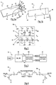
- the balanced antenna system 10 is reconfigurable, as will be described in more detail below, and is designed for use in a portable product such as a mobile phone, laptop or PDA.
- the balanced antenna system 10 is provided on a microwave substrate 12 (e.g. a printed circuit board, PCB) having a surface area of approximately 116 ⁇ 40 mm 2 and a thickness of approximately 1.15mm so that the system can easily be accommodated in a conventional mobile phone.
- a microwave substrate 12 e.g. a printed circuit board, PCB
- a first radiating element 14 is provided on a first side 16 of the substrate 12, at a first end portion 18 thereof.
- the first radiating element 14 is formed from a substantially U-shaped first strip layer 20 which is located in one half of the first end portion 18 of the substrate 12 and is orientated such that its open end 22 faces inwardly towards the central region of the first end portion 18.
- a short feed line 24 is provided at a start of the first strip 20 closest to the centre of the substrate 12 and extends along the length of the substrate 12.
- the second radiating element 26 is therefore formed from a substantially U-shaped second strip layer 28 which is also orientated such that its open end 30 faces inwardly towards the central region of the first end portion 18.
- a short feed line 32 is again provided at a start of the second strip 28 closest to the centre of the substrate 12 and extends along the length of the substrate 12.
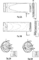
- a gap 34 is provided between the respective feed lines 24, 32 of the first and second radiating elements 14, 26 and between the respective ends 36 of the first and second strips 20, 28. Accordingly, the first and second radiating elements 14, 26 form a dipole antenna 37. In the embodiment shown in Figure 1A , the first and second radiating elements 14, 26 together extend over an area of approximately 40 ⁇ 10 mm 2 .
- a ground plane 38 is provided on a second side 40 of the substrate 12, opposite to the first side 16.
- the ground plane 38 is substantially rectangular and occupies substantially the whole of the substrate 12 surface from a second end 42 thereof (opposite to the first end portion 18) to a position substantially opposite the feed lines 24, 32.
- the ground plane 38 has a size of approximately 100 ⁇ 40 mm 2 .
- the balanced antenna system 10 also includes a balun and two matching circuits which are connected to the first and second radiating elements 14, 26 and which are not shown in Figures 1A and 1B for reasons of clarity but which would be provided on the first side 16 of the substrate 12, opposite to the ground plane 40.
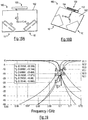
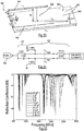
- balun 50 An example of a suitable balun 50 is shown in Figure 2 by way of an LC circuit diagram.
- This particular balun 50 has a wideband configuration and is substantially as described by Iizuka and Watanabe in published Japanese patent application number 2005-198167 .
- the balun 50 comprises a first (unbalanced) port Z u forming an input to a T-junction 52 which is configured to split an electrical signal received at the first port Z u into a high path 54 and a low path 56.
- the high path 54 is arranged to feed into a first high pass filter (HPF) and the low path is arranged to feed into a second low pass filter (LPF).
- HPF high pass filter
- LPF second low pass filter
- the high pass filter is constructed from an L-C circuit having three capacitors connected in series C H1 , C H2 , C H1 and two inductors L H1 , L H1 connected in parallel from respective branches provided between the capacitors.
- Each of the inductors L H1 is connected to the ground plane 40 and the output from the capacitors C H1 , C H2, C H1 constitutes an impedance Z bH .
- the low pass filter is constructed from an L-C circuit having three inductors connected in series L L1 , L L2 , L L1 and two capacitors C L1 , C L1 connected in parallel from respective branches provided between the inductors.
- Each of the capacitors C L1 is connected to the ground plane 40 and the output from the inductors L L1 , L L2 , L L1 constitutes an impedance Z bL .
- Z bH and Z bL form a balanced output Z b .
- the balanced antenna system 10 comprises the balun 50 shown in Figure 2 , used to feed the balanced dipole antenna 37 shown in Figure 1A , with an impedance matching circuit 60 provided therebetween.
- an input Port 1 is shown which feeds into the first (unbalanced) port Z u of the balun 50 to drive the balanced antenna system 10.
- the high pass filter with impedance Z bH from the balun 50 is connected to the matching circuit 60 and to Feed 1 (i.e. feed line 24 of Figure 1A ) of the dipole antenna 37 and the low pass filter with impedance Z bL from the balun 50 is connected to the matching circuit 60 and to Feed 2 (i.e. feed line 32 of Figure 1A ) of the dipole antenna 37.
- the system can be made reconfigurable and can be used to provide a wide tuning range of from 470MHz to 2200MHz, which can cover DVB-H, all GSM and UMTS2100 frequency bands.
- Figure 4 shows a circuit diagram for a particular impedance-matching circuit 60 which can be used in an embodiment of the present invention. It will be noted that in this illustration, the paths for the high pass filter with impedance Z bH and the low pass filter with impedance Z bL from the balun 50 to Feed 1 and Feed 2 respectively, have been separated out such that the impedance-matching circuit 60 is split into a first matching circuit 62 and a second matching circuit 64.
- the first and second matching circuits 62, 64 are identical and are configured to provide impedance transformation to each leg of the balanced dipole antenna 37.
- each of the first and second matching circuits 62, 64 comprise an inductor L 2 connected in parallel to the ground plane 40 and a capacitor C 1 /C 2 and inductor L 1 connected in series.
- the capacitors C 1 /C 2 are variable so as to allow the impedance of the first and second matching circuits 62, 64 to be adjusted to tune the antenna 37 over a range of frequencies.
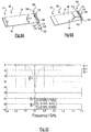
- FIG. 4 While the embodiment shown in Figure 4 can enable tuning over a certain range of frequencies it has been discovered that a greater tuning range can be achieved by including multiple balun configurations and multiple impedance-matching configurations into an integrated tuning circuit 70, such as illustrated in Figure 5 .
- input Port 1 (unbalanced feed-line) is provided at the left-hand side of the circuit 70 and the unbalanced feed-line is converted to two balanced feed-lines via the balun configuration 72.
- the high pass filter is connected to a first impedance matching circuit 74 and to the balanced dipole antenna 37 via Feed 1
- the low pass filter is connected to a second impedance matching circuit 76 and to the balanced dipole antenna 37 via Feed 2.
- the balun configuration 72 comprises a first high pass filter 78 and a second high pass filter 80 which are identical in construction to the high pass filter described above in relation to Figure 2 but which have different values for each of the capacitors and inductors.
- a first (signal pole double throw) switch 82 is provided to select one of the first or second high pass filters 78, 80 to be employed at any one time.
- a first low pass filter 84 and a second low pass filter 86 are also provided which are identical in construction to the low pass filter described above in relation to Figure 2 but which again have different values for each of the capacitors and inductors.
- a second (signal pole double throw) switch 88 is provided to select one of the first or second low pass filters 84, 86 to be employed at any one time.
- the first impedance matching circuit 74 is of the form described above in relation to Figure 4 but includes three different inductors (L7, L8, L9) which can be selected as the inductor in parallel (L 2 ) and three further different inductors (L1, L2, L3) which can be selected as the inductor in series (L 1 ).
- Various switches are provided in order to activate the desired combination of components for the first impedance matching circuit 74.
- a tunable capacitor C 1 i.e. varactor
- the tunable capacitor C 1 can be tuned from 0.2pF to 10pF.
- the second impedance matching circuit 76 is of the form described above in relation to Figure 4 but also includes three different inductors (L14, L15, L16) which can be selected as the inductor in parallel (L 2 ) and three further different inductors (L4, L5, L6) which can be selected as the inductor in series (L 1 ).
- Various switches are provided in order to activate the desired combination of components for the second impedance matching circuit 76.
- a tunable capacitor C 2 i.e. varactor
- the tunable capacitor C 2 can be tuned from 0.2pF to 10pF.
- the circuit shown in Figure 5 was designed using a simulation tool (CST Microwave Studio®) in which the antenna structure of Figures 1A and 1B was simulated using the transient solver to produce a 1-Port S-Parameter file representing the antenna response and this was used as a starting point for designing the matching networks.
- the values of the components within the first and second matching circuits 74, 76 were calculated using standard formulas available within the literature.
- Microwave Office an RF/microwave design platform available from AWR Corporation
- the capacitors C 1 and C 2 were fixed to 10 pF respectively during this phase of the design process. It is noted that the same simulation tool was used for all simulations described herein.
- Table 2 below lists the required logic states for the switches shown in Figure 5 in order to produce the required spectrum coverage.
- a single pole double throw switch such as switch 82 in Figure 5
- a '0' represents the situation where nodes labelled 1 and 2 are connected and nodes labelled 4 and 5 are connected while a '1' represents the situation where nodes labelled 1 and 3 are connected and nodes labelled 4 and 6 are respectively connected.
- each of the switches is shown in a default position.
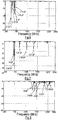
- Table 2 Operating logic states Modes X Y Z Operating band OUTPUT (MHz) A 1 1 0 470-640 B 1 0 0 630-1520 C 0 0 1 1500-2200
- Mode A, B, and C relate to the three relatively narrow bands of operation of the antenna.
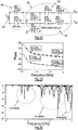
- Mode A operation it is possible to move the resonant frequency from 470 MHz to 640 MHz by varying the varactors C 1 and C 2 together from 10 pF to 1.11 pF as illustrated in Figure 6 .
- Figure 7 illustrates Mode B operation in which the resonant frequency can be tuned from 630 MHz to 1520 MHz by varying the varactors C 1 and C 2 together from 10 pF to 0.21 pF.
- Figure 8 illustrates Mode C operation when the varactors C 1 and C 2 together are varied from 10 pF to 0.38 pF and the resonant frequency is moved from 1500 MHz to 2200 MHz.
- the simulation results using ideal components show that the present antenna structure has wide tuning range of 1730 MHz. Accordingly, the resonant frequency of the antenna can be tuned to cover DVB-H, GSM710, GSM850, GSM900, GPS1575, GSM1800, PCS1900 and UMTS2100 bands.
- tuning may achieved by setting each varactor to a different value.
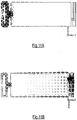
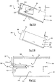
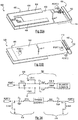
- An antenna structure 90 suitable for Multiple-Input-Multiple-Output (MIMO) applications is illustrated in Figures 9A and 9B in accordance with another embodiment of the present invention.
- the antenna structure 90 comprises the balanced antenna system 10 described above in combination with a two-port chassis antenna 100.
- MIMO devices utilise multiple uncorrelated channels/antennas to increase the capacity of a communication link without the need of additional spectrum or transmitter power.
- the uncorrelated antennas should be terminated at an optimal location to induce a required (or best) antenna-to-antenna isolation.
- the best isolation values are often achieved when the antennas are spaced by the largest available distance (e.g. one at the top edge of the substrate 12 and the other at the bottom edge). In this particular embodiment, the antennas are separated along the length of the substrate 12 by a distance of approximately 100 mm.
- MIMO systems according to the present invention are described.
- the MIMO system comprises two separate antennas. While in the forth case, the MIMO system comprises three separate antennas.
- the two-port chassis antenna 100 is of the type described in detail in GB0918477.1 and comprises a pair of non-resonant coupling elements 112, 114, that are capable of simultaneous dual-band operation.
- the coupling elements 112, 114 occupy a relatively small volumetric space of 40 ⁇ 5 ⁇ 7 mm 3 and are located on the top of a chassis 116 on the same side as the second side 40 of the substrate 12, while the dipole antenna 37 of the balanced antenna system 10 is located on the opposite first side 16.
- the two coupling elements 112, 114 are mounted in close proximity to each other and are driven over the ground plane 38.
- the first coupling element 112 is constituted by an L-shaped metal patch having a planar portion which constitutes the chassis 116, parallel to the ground plane 38, and an orthogonal portion 118, orthogonal to the ground plane 38.
- the planar portion 116 is provided on the opposite side of the substrate from the ground plane 38 and is laterally spaced therefrom.
- the orthogonal portion 118 extends from an edge of the planar portion 116 furthest from the ground plane 38 such that the orthogonal portion 118 is spaced from the ground plane 38 by a so-called first gap 120.
- the first gap 120 is less that 10mm.
- the second coupling element 114 is also constituted by a metal patch which, in this case, forms a planar rectangle.
- the second radiating element 114 is also orientated orthogonally to the ground plane 38 and is located within the first gap120.
- the second radiating element 114 is effectively enclosed on two adjacent sides by the L-shaped first coupling element 12.
- the second coupling element 114 is approximately half the length of the first coupling element 112 and is slightly inset from the edge of the first coupling element 112.
- the distance between the ground plane 38 and the second coupling element 114 forms a so-called second gap 122.
- the distance between the second coupling element 114 and the orthogonal portion 118 of the first coupling element 12 determines the amount of mutual coupling therebetween. This distance is therefore referred to as the mutual gap 124.
- each radiating element 112, 114 is connected, respectively, to a first and second control module via a second and third feed port 126, 128.
- the second feed port 126 extends between the orthogonal portion 118 of the first coupling element 112 and a first control module (not shown), and is located approximately one third of the distance along the length of the first coupling element 112.
- the third feed port 128 (Port 3) is located adjacent to the second feed port 126 and connects to an adjacent second control module (not shown).
- each coupling element 112, 114 can be selectively driven independently, allowed to float, or tied to the ground state through operation of the respective control modules.
- Port 1 was connected to a circuit similar to that shown in Figure 5 and only Port 2 was activated in connection with the chassis antenna 100. More specifically, Port 2 was connected to a circuit of the type described in GB0918477.1 and Port 3 was simply connected to a 50 ohm load but could have been tuned separately.
- Figure 10 shows a graph of S parameters for the MIMO antenna structure of Figures 9A and 9B under the circumstances described above.
- the return loss for the balanced antenna system 10 was found to be approximately -11.62 dB while the return loss for Port 2 of the chassis antenna 100 was approximately -35.92dB.
- the S21 return loss (which is a measure of the isolation between the balanced antenna 10 and the chassis antenna 100) is approximately -30.53 dB.
- FIGS 12A and 12B also corroborate this result through an illustration of the average current distribution when either the balanced antenna 10 is driven or the chassis antenna 100 is driven.
- FIGs 14A and 14B show, respectively, a front view and a rear view of another combined MIMO antenna system 140 comprising the balanced antenna 10 of Figures 1A and 1B and the chassis antenna 100 of Figures 9A and 9B but, in this case, the chassis antenna 100 is mounted on the side rather than the end of the substrate 12.
- the chassis antenna 100 is still mounted towards the opposite end of the substrate 12 (and on the opposite side of the substrate) when compared to the balanced antenna 10, so as to provide the largest possible separation between the two antennas in this configuration.
- the antennas are separated along the length of the substrate 12 by a distance of approximately 60mm.
- Port 1 was connected to the balanced antenna 10 and driven by the circuit of Figure 5
- Port 2 was connected to the large coupling element 112 (driven by a matching circuit of the type described in GB0918477.1 ) and Port 3 was connected to the small coupling element 114 and was simply tied to a 50 ohm load.
- Figure 15 illustrates that the return loss for the balanced antenna 10, incorporating a matching network of Figure 5 , is about -22.16 dB while the return loss for the chassis antenna 100 is about -46.98 dB. It is also clear from Figure 15 that the S12 isolation between the balanced antenna 10 and the chassis-antenna 100 is about -22.62 dB.
- Figures 16A and 16B show, respectively, a front view and a rear view of another combined MIMO antenna system 150 comprising the balanced antenna 10 of Figures 1A and 1B plus a second balanced antenna 152 (which is identical to that of Figures 1A and 1B ) and which is mounted towards the opposite end of the substrate 12 (and on the same side of the substrate 12) when compared to the balanced antenna 10, but is orientated orthogonally to the balanced antenna 10 is located along the top edge as viewed. As illustrated, the antennas are separated along the length of the substrate 12 by a distance of approximately 60mm.
- Port 1 is connected as described above and Port 2 is connected to the second balanced antenna 152 and to a further optimized circuit similar to that shown in Figure 5 .
- Figure 17 illustrates the S parameters for the MIMO antenna system 150 when each of the antennas are connected to the respective matching networks.
- the return loss for the balanced antenna 10 is about -11.12 dB while the return loss for the second balanced antenna 152 is about -9.52 dB. It can also be seen that the S12 isolation between the two balanced antennas is about -17.65 dB in this embodiment.
- FIGs 18A and 18B show, respectively, a front view and a rear view of another combined MIMO antenna system 160 comprising two balanced antennas 10 (which are identical to those described in relation to Figures 1A and 1B ) plus the chassis antenna 100 described in relation to Figures 9A and 9B .
- the substrate 162 has an area of approximately 90 ⁇ 66 mm 2
- the chassis antenna 100 is mounted in the middle of the long side of the substrate 162
- the two balanced antennas 10 are mounted towards each of the two corners of the substrate 162 furthest from the chassis antenna 100.
- the two balanced antennas 10 are also orientated at an inwardly inclined angle of approximately 45° with respect to the length of the substrate 162.
- the two balanced antennas 10 are each separated from the chassis antenna 100 in a direction along the short dimension of the substrate 162 by about 30.64 mm and are separated from each other along the long dimension of the substrate 162 by about 19.29 mm.
- Port 1 and Port 2 are connected to each of the balanced antennas 10 and their respective matching circuits and Port 3 is connected to the large coupling element 112 of the chassis antenna 100 (and its optimized matching circuit).
- the small coupling element 114 is left as an open circuit in this embodiment.
- Figure 19 illustrates that the return loss for the first of the balanced antennas 10, incorporating the matching network, is about -28.32 dB while the return loss for the second of the balanced antennas 10, incorporating the matching network, is about - 12.14 dB, and the return loss for the large coupling element 112, incorporating the matching network, is about -23.41 dB. Fit is also shown that the isolations between these antennas are about -10.885 dB between the two balanced antennas, -16.88 dB between the chassis antenna and the second balanced antenna and -17.07 dB between the chassis antenna and the first balanced antenna.
- FIG 20 shows a circuit diagram for an alternative balun 170 which may be used in embodiments of the present invention.
- the balun 170 comprises an LC circuit substantially as described by Yeh, Liu and Chiou in 'Compact 28-GHz Subharmonically Pumped Resistive Mixer MMIC Using a Lumped-Element HighPass/Band-Pass Balun', published in IEEE Microwave and Wireless Components Letters, Vol. 15, No.2, February 2005 .
- the balun 170 comprises a high pass filter (first filter) 172 and a band pass filter (second filter) 174.
- a first (unbalanced) port Z u is connected to the high pass filter 172 and the band pass filter 174 via a T-junction.
- the high pass filter 172 comprises a capacitor C and an inductor L, and the output from which constitutes an impedance Z b1 .
- the band pass filter 174 comprises three inductors and two compactors, and the output from which constitutes an impedance Z b2 .
- the inductors L are all identical but, in the band pass filter 174, one of the capacitors (constituting a shunt capacitor labelled 2C) is double the value of other capactors C.
- the balun 170 is essentially an out-of-phase power splitter which includes one high pass filter 172 and one band pass filter 174 connected in parallel. Although this balun 170 can provide wide bandwidth operation (and has fewer components than the balun 50 described above, resulting in less loss), in practice, the balun 170 may provide less than 180 degrees of phase difference between the unbalanced outputs Z b1 and Z b2 . Thus, in embodiments where a 180 degree phase difference is required it may be more convenient to employ a balun of the type shown in Figure 2 and in embodiments where a 180 degree phase difference is not required it may more convenient to employ a balun of the type shown in Figure 20 .
- balun 170 is employed in embodiments of the invention, it is possible to obtain the desired tuning range of about 470 to 2200 MHz by employing only one balun 170 configuration and only two configurations for each of the first and second matching circuits. Thus, a simpler circuit can be employed when compared to the embodiment shown in Figure 5 .
- a balanced antenna system 200 according to a further embodiment of the present invention is illustrated in Figures 21A through 21C .
- the balanced antenna system 200 is reconfigurable, as will be described in more detail below, and is designed for use in a portable product such as a mobile phone, laptop or PDA.
- the balanced antenna system 200 is provided on a microwave substrate 202 (e.g. a printed circuit board, PCB) having a length L 1 of approximately 110mm, a width W of approximately 40mm and a thickness H of approximately 5mm so that the system can easily be accommodated in a conventional mobile phone.
- a microwave substrate 202 e.g. a printed circuit board, PCB
- a first radiating element 204 is provided on a first side 206 of the substrate 202, at a first end portion 208 thereof.
- the first radiating element 204 is constituted by a substantially L-shaped first strip layer which is located in one half of the substrate 202 towards the first end portion 208 and is orientated such that its open side 212 faces inwardly towards the central region of the first end portion 208.
- a short feed line 214 is provided at a start of the first radiating element 204 closest to the centre of the substrate 202 and extends along the length of the substrate 202.
- a second radiating element 216 which is substantially similar to the first radiating element 204, is also provided on the first side 206 of the substrate 202 and is located in an adjacent half of the first end portion 208 of the substrate 202.
- the second radiating element 216 is therefore constituted by a substantially L-shaped second strip layer which is also orientated such that its open side 220 faces inwardly towards the central region of the first end portion 208.
- the second radiating element 216 is orientated in an opposite direction to the first radiating element 204.
- a short feed line 222 is again provided at a start of the second radiating element 216 closest to the centre of the substrate 202 and extends along the length of the substrate 202.
- a gap 224 is provided between the respective feed lines 214, 222 of the first and second radiating elements 204, 216 and between the respective ends 226 of the first and second strips. Accordingly, the first and second radiating elements 204, 216 form a large dipole antenna 227.
- the first and second radiating elements 204, 166 have a long side l 1 extending approximately 70mm along the length of the substrate 202 and a short side l 2 extending approximately 19mm along the width of the substrate 202.
- the width w of each of the first and second strips is approximately 1mm and the gap 224 has an extent d of approximately 2 mm.
- Each of the feed lines 214, 222 has a length l 3 of approximately 10 mm.
- a ground plane 228 is provided on a second side 230 of the substrate 202, opposite to the first side 206.
- the ground plane 228 is substantially rectangular and occupies substantially the whole of the substrate 202 surface from a second end 232 thereof (opposite to the first end portion 208) to a position substantially opposite the free ends of the feed lines 214, 222.
- the ground plane 228 has a length L 2 of approximately 100mm and extends over the entire width W of the substrate 202.
- the balanced antenna system 200 also includes a balun and two matching circuits which are connected to the first and second radiating elements 204, 216 and which are not shown in Figures 21A through 21C for reasons of clarity but which would be provided on the first side 206 of the substrate 202, opposite to the ground plane 228.
- FIG 22 shows a circuit diagram of a suitable balun 240 and matching circuit arrangement 250 for the antenna 200 of Figures 21A through 21C .
- the balun 240 comprises one inductor L5 (of 1nH) and one capacitor C3 (of 0.1pF) which are connected in parallel branches from a T-junction 242 which splits an unbalanced signal Z u .
- the matching circuit arrangement 250 comprises a first matching circuit 252 connected to the inductor L5 of the balun 240 and which terminates in a balanced signal Z b1 which in practice is fed into the feed line 214 of the first radiating element 204, and a second matching circuit 254 connected to the capacitor C3 of the balun 240 and which terminates in a balanced signal Z b2 which in practice is fed into the feed line 222 of the second radiating element 216.
- the first and second matching circuits 252, 254 each comprise an inductor L3, L4 (each of 3.5nH), a capacitor C1, C2 (each of 10pF) and a second inductor L1. L2 (each of 9.4nH).
- the capacitor C1, C2 may be replaced by a varactor capable of varying from 10 pF to 0.2 pF.
- the integration of the first and second matching circuits 252 and 254 and the balun 240 has been optimised to produce a required phase difference of about 180° in order to transfer the balanced feeds Z b1 and Z b2 to the unbalanced feed Z u within a required operating bandwidth.
- Figure 24 shows simulated reflection coefficients against frequency for the large balanced antenna 200 when fed by the circuit of Figure 22 .
- the balanced antenna is configured to provide three resonances simultaneously and the varactors (denoted as C 1 and C 2 ) in the matching circuit arrangement 250 can be varied from 10 pF to 0.2 pF to move the three resonant frequencies simultaneously to cover the low-band (from 700 MHz to 1010 MHz), the mid-band (from 1620 MHz to 2490 MHz) and the high-band (from 2740 MHz to over 3000 MHz), while maintaining a return loss above 6dB.
- the present antenna structure 200 is able to provide high efficiency within the required operating bands even when taking into account the loss of real components. Further optimisation of the antenna structure or the addition of further matching circuits could be used to cover any remaining frequency bands of interest.
- FIGS 25A, 25B and 25C show a reconfigurable balanced dipole antenna 300 according to another embodiment of the present invention, which has a single tunable resonant frequency.
- the balanced antenna 300 is provided on a microwave substrate 302, Taconic TLY-3-0450-C5, which has a permittivity of 2.33, loss tangent of 0.0009, a thickness of 1.143 mm, a length L 1 of approximately 114mm and a width W of approximately 40mm.
- the antenna 300 comprises two metallic radiating elements 304 mounted at a first end 306 of the substrate 302 and which extend substantially over the width W of the substrate 302, such that they occupy a total area of approximately 40mm ⁇ 14mm.
- the radiating elements 304 have a metal thickness of 0.01778 mm and are mounted at a height H of 5mm above the substrate 302, for example using spacers (not shown).
- the antenna 300 can easily be accommodated in a conventional mobile phone.
- a metal ground plane 307 is provided on a rear of the substrate 302.
- the ground plane 307 occupies an area of 100 ⁇ 40mm 2 and terminates at a position opposite the end of the region where the radiating elements 304 are disposed.
- the radiating elements 304 are symmetrically arranged on either side of a central longitudinal axis of the substrate 302 such a gap d of 2mm is provided between each radiating element 304.
- each radiating element 304 is substantially rectangular, an L-shaped cut-out 308 is provided adjacent the first end 306 such that an inner portion 310 of each rectangle is missing at the first end 306 and a transverse slit 312 is provided a short distance from the first end 306, which extends from the missing inner portion 310 to a position close to but spaced from the edge of the substrate 302.
- a feed line 315 is provided adjacent an inner edge of each of the radiating elements 304, at the end opposite to the first end 306, for connecting the radiating elements 304 to a control circuit as will be described below.
- Table 3 Dimensions for the antenna shown in Figures 25A to 25C H 5 mm w 4 12mm W 40 mm w 5 14 mm L 1 114 mm l 1 2 mm L 2 100 mm l 2 10 mm w 1 14 mm l 3 2 mm w 2 5 mm l 4 2 mm w 3 17 mm l 5 12 mm
- FIG 26 shows a circuit diagram comprising a balun 320 and matching circuit 322 for the antenna 300 of Figures 25A through 25C .
- the balun 320 and matching circuit 320 are provided on the substrate 302, opposite to the ground plane 307 and are connected to the radiating elements 304 via the feed lines 315.
- the balun 320 comprises an inductor of 10.4nH and a capacitor of 1.9pF connected in parallel.
- the matching circuit 322 comprises two identical circuits, each of which is connected between a branch of the balun 320 and one of the radiating elements 304, and comprises an inductor of 1.3nH connected in parallel with a varactor C 1 of up to 10pF, which in turn is connected in series with an inductor of 41nH.
- the varactors C 1 of Figure 26 from 10pF to 0.1pF it is possible to tune the frequency of the antenna 300 from approximately 700 MHz up to 2434 MHz, with at least 6dB return loss.
- the antenna 300 has high dissipated loss on the lumped elements in the circuit and low efficiency at low frequency such as 700 MHz, its size is suitable for MIMO applications in small terminals, for example, Watch Cell Phones.
- a reconfigurable balanced antenna of the same structure as illustrated in Figures 21A to 21C and having the dimensions detailed in table 4 below.
- Table 4 Dimensions for the antenna shown in Figures 21A to 21C H 5 mm L 1 110 mm W 40 mm L 2 100 mm l 1 50 mm l 2 19 mm l 3 10 mm d 2 mm w 1 mm - -
- the antenna comprises L-shaped dipole arms, 50mm ⁇ 40mm in size, with a 1 mm track width, a metal thickness of 0.01778 mm and has a total size of 110 ⁇ 40mm 2 and ground plane size of 100 ⁇ 40mm 2 .
- the antenna was constructed on a microwave substrate material, Taconic TLY-3-0450-C5, which has a permittivity of 2.33, loss tangent of 0.0009 and a thickness of 1.143 mm.
- FIG. 28 shows a circuit diagram for the antenna described above.
- This circuit comprises a balun 330 and matching circuit 332 which would be provided on the substrate 202, opposite to the ground plane 228 and would be connected to the radiating elements 204, 216 via the feed lines 214, 222.
- the balun 330 comprises an inductor of 12nH and a capacitor of 2pF connected in parallel.
- the matching circuit 332 comprises two identical circuits, each of which is connected between a branch of the balun 330 and one of the radiating elements 204, 216, and comprises an inductor of 7.3nH connected in parallel with a varactor C 1 of up to 10pF, which in turn is connected in series with an inductor of 26nH.
- Figure 30 shows a front and rear view of a further reconfigurable balanced antenna 400 according to an embodiment of the present invention.
- the antenna 400 is similar to that described above and shown in Figures 21A through 21C but this time has the dimensions detailed in Table 5 below.
- Table 5 Dimensions for the antenna showed in Figure 30 H 5 mm L 1 110 mm W 40 mm L 2 100 mm l 1 70 mm l 2 19 mm l 3 10 mm d 2 mm w 1 mm - -
- the antenna 400 comprises L-shaped dipole radiating elements 404, 70 mm ⁇ 40 mm in size, with a 1mm track width, a metal thickness of 0.01778 mm and has a total size of 110 ⁇ 40mm 2 and ground plane 406 of 100 ⁇ 40mm 2 .
- the antenna was constructed on a microwave substrate material 402, Taconic TLY-3-0450-C5, which has a permittivity of 2.33, loss tangent of 0.0009 and a thickness of 1.143 mm.
- a port 408 is provided on the ground plane 406 for driving the radiating elements 404 via a suitable circuit.
- FIG 31 shows such a circuit diagram for the antenna 400.
- This circuit comprises a balun 410 and matching circuit 412 which would be provided on the substrate 402, opposite to the ground plane 406 (but drivable through the port 408) and would be connected to the radiating elements 404 via feed lines.
- the balun 410 comprises an inductor of 13.2nH and a capacitor of 2.3pF connected in parallel.
- the matching circuit 412 comprises two identical circuits, each of which is connected between a branch of the balun 410 and one of the radiating elements 404, and comprises an inductor of 1.9nH connected in parallel with a varactor C 1 of up to 10pF, which in turn is connected in series with an inductor of 9.4nH.
- the low-band and mid-band can cover most of the existing cellular services, since the low-band can be tuned to cover LTE700, GSM850 and EGSM900 and the mid-band can be tuned to cover PCN, GSM1800, GSM1900, PCS and UMTS.
- the applicants have also found that incorporating real components provides at least -3.77 dB of total efficiency at 684 MHz. It is therefore believed that the antenna 400 can address the low efficiency problem that may be associated with some of the previous embodiments at low frequencies.
- FIGs 33A and 33B show, respectively, a front and rear view of another balanced antenna 500 according an embodiment of the present invention and which is suitable for Multiple-Input-Multiple-Output (MIMO) applications.
- the antenna 500 essentially comprises the antenna 400 of Figure 30 combined with a two-port chassis-antenna 100 as shown in Figures 9A and 9B and as described above.
- the two-port chassis antenna 100 is of the type described in detail in GB0918477.1 and comprises a pair of non-resonant coupling elements 112, 114, that are capable of simultaneous dual-band operation.
- the MIMO antenna 500 has a total size of 118 ⁇ 40 mm 2 and a ground plane 502 of 100 ⁇ 40 mm 2 .
- the chassis antenna 100 occupies a small volume of 40 ⁇ 4 ⁇ 7 mm 3 and is mounted off a second end of the substrate 402, opposite to the end where the radiating elements 404 are disposed.
- the radiating elements 404 are provided on an additional U-shaped substrate 504 which is wider and longer than the radiating elements 404 themselves, to provide mechanical support.
- the balanced antenna element 400 and the coupling elements 112, 114 in the chassis antenna 100 are supported by RohacellTM material.
- a first port, Port 1 is provided through the ground plane 502 for driving the radiating elements 404 via a suitable circuit.
- a second port, Port 2 is provided on an edge of the substrate 402 for driving coupling element 114 and a third port, Port 3, is provided through the second end of the ground plane 502 for driving coupling element 112.
- FIG 34 shows circuit diagrams for the elements provided between each of the ports and their respective radiating and coupling elements 404, 112, 114.
- Port 1 is connected to a balun 510 comprising an inductor of 13nH and a capacitor of 3pF connected in parallel.
- Each arm of the balun 510 is then connected to one of the radiating elements 404 via an identical matching circuit 512.
- Each matching circuit 512 comprises an inductor of 1.9nH connected in parallel with a varactor C 1 of up to 10pF, which in turn is connected in series with an inductor of 5.6nH.
- a first L-network matching circuit 514 is connected between Port 2 and coupling element 114 and a second L-network matching circuit 516 is connected between Port 3 and coupling element 112.
- the first matching circuit 514 comprises a parallel inductor of 5.1nH connected to a varactor C 2 of up to 10pF, which in turn is connected in series to an inductor of 27nH.
- the second matching circuit 516 comprises a parallel inductor of 2.4nH connected to a varactor C 3 of up to 10pF, which in turn is connected in series to an inductor of 2nH.
- the MIMO antenna 500 was simulated in CST Microwave Studio® and the s4p file representing the frequency response of the antenna was then used to determine the optimum component values detailed above for each matching circuit using Microwave Office, from Applied Wave Research..
- the antenna 500 was also demonstrated with the four varactor diodes C 1 , C 1 , C 2 , C 3 being of the type MV34003-150A, having a capacitance variable from 0.409 pF to 15.435 pF (which was broader than the range described above) for an applied voltage of 0 V to 15 V.
- a dc bias line incorporating a 10 k ⁇ resistor, was attached to the anode of each varactor to supply positive voltage. The resistor was employed for damping any residual RF signals appearing on the dc line.
- the negative voltage was supplied from an inner conductor of an SMA connector (i.e. a coaxial RF connector having a 50 Ohm impedance) by using a bias-tee ZX85-122G-S+, from Mini-Circuits®.
- Figure 35 shows measured reflection coefficients against frequency for when the varactors in the circuit of Figure 34 are varied from approximately 15.4 pF to 0.4 pF.
- the antenna 500 can be operated in three simultaneous bands. Ports 2 and 3, of the chassis-antenna 100, were open circuit during the measurement. The voltage across the varactors was varied from 0 V to 15 V and the resulting resonant frequencies varied from 646 MHz to 848 MHz for the low band, 1648 MHz to 2074 MHz for the mid-band and 2512 MHz to over 3000 MHz for high band, while maintaining a return loss above 6 dB.
- Table 6 below shows the measured reflection coefficient for both ports of the chassis-antenna 100 while the varactor voltages are varied from 0 V to 15 V. During measurements on each port, the other two ports are left open circuit. Unlike the balanced antenna 400 each port of the chassis antenna 100 drives a single resonance. The frequencies of each port vary from 597 MHz to 1124 MHz and 1586 MHz to 2332 MHz, respectively. Thus, the antenna 500 provides MIMO operation from 646 MHz to 848 MHz and 1648 MHz to 2074 MHz. It is also likely that the frequency tuning range could be increased, if the capacitance tuning range of the varactors was wider.
- the instantaneous bandwidth at various frequencies for ports 2 and 3 are also shown in Table 6.
- the bandwidth of port 1 for the same frequencies is also shown. The smallest of these thus represent the instantaneous MIMO bandwidth. It can be seen that port 2 gives a considerably narrower bandwidth than port 3.
- Table 6 shows that the minimum MIMO bandwidth is 14 MHz (at 771 MHz centre frequency) and the maximum MIMO bandwidth is 93 MHz (at 1812 MHz centre frequency).
- Table 6 Measured refection coefficients for Ports 2 and 3 (Chassis Antenna) as varactors varied from 0V to 15V respectively Voltage (V) Freq. (MHz) Refl. Coeff.
- Table 7 gives the measured S parameters for the MIMO antenna 500. It is clear from these results that isolation is good as S21 is at least 15 dB over all of the bands. Table 7 Measured S parameters for the MIMO antenna of Figure 33A-B *applied voltage to the varactors of the balanced antenna Voltage (V) Ports Frequency (MHz) S11 (dB) S22 (dB) S21 (dB) 0* & 1.3 + 1 & 2 646 -16.85 -32.14 -20.15 1.72* & 2.53 + 1 & 2 710 -16.25 -27.21 -17.17 6.85* & 5.6 + 1 & 2 850 -10.85 -36.53 -18.25 0* & 1.1 + 1 & 3 1645 -14.62 -25.36 -26.57 1.9* & 2.1 + 1 & 3 1710 -16.01 -18.71 -25.40 12* & 6.4 + 1 & 3 2050 -13.09 -14
- Figure 36 shows a view similar to that of Figure 33B but wherein the ground plane 502 has been modified to include a U-shaped slot 520 around Port 1.
- the MIMO antenna 500 it is desirable for the MIMO antenna 500 to have a total efficiency of at least -4.5 dB for the main transmission and reception antenna (e.g. the chassis antenna 100) and -5.5 dB for the second reception antenna (e.g. the balanced antenna 400).
- the realized gain of the chassis antenna 100 when integrated with the balanced antenna 400 in accordance with Figures 33A and 33B , dropped at least 5 dB at low frequencies.
- the applicants have proposed to isolate the matching circuits of the balanced antenna 400 and the chassis antenna 100 by introducing the slot 520 in the ground plane 502, as shown in Figure 36 .
- Table 8 below shows the simulated reflection coefficient, radiation efficiency, total efficiency and realized gain for the MIMO antenna 500 including the slot 520, as shown in Figure 36 .
- the realized gain for the chassis-antenna 100 has been improved by 6.28 dB (79.6%), since it is now -7.89dB at 687 MHz, without affecting other parameters, simply by including the slot 520.
- Table 8 Simulated reflection coefficient, radiation efficiency, total efficiency and realized gain for the antenna of Figure 36 Balanced Antenna Chassis-Antenna Capacitor For Balanced Antenna Frequency (MHz) Simulated Refl. Coe. (dB) Simulated Rad. Effic. (dB) Simulated Tot. Effic.
- embodiments of the present invention can provide a reconfigurable balanced antenna which can be tuned over a wide range of frequencies (e.g. from 646 MHz to over 3000 MHz) and which can be incorporated along with another antenna into a MIMO antenna structure which has good antenna isolation.
- the balanced antenna may be able to cover the existing cellular service bands known as DVB-H, GSM710, GSM850, GSM900, GPS1575, GSM1800, PCS1900 and UMTS2100 and is an ideal candidate for MIMO applications, especially in small terminals such mobile devices, laptops and PDAs.
Applications Claiming Priority (3)
| Application Number | Priority Date | Filing Date | Title |
|---|---|---|---|
| GBGB1020202.6A GB201020202D0 (en) | 2010-11-29 | 2010-11-29 | Balanced antenna system |
| GBGB1108456.3A GB201108456D0 (en) | 2011-05-19 | 2011-05-19 | Balanced antenna system |
| PCT/GB2011/001598 WO2012072969A1 (en) | 2010-11-29 | 2011-11-11 | Balanced antenna system |
Publications (2)
| Publication Number | Publication Date |
|---|---|
| EP2647124A1 EP2647124A1 (en) | 2013-10-09 |
| EP2647124B1 true EP2647124B1 (en) | 2019-06-05 |
Family
ID=45048136
Family Applications (1)
| Application Number | Title | Priority Date | Filing Date |
|---|---|---|---|
| EP11788553.3A Active EP2647124B1 (en) | 2010-11-29 | 2011-11-11 | Balanced antenna system |
Country Status (6)
| Country | Link |
|---|---|
| US (2) | US9553361B2 (ko) |
| EP (1) | EP2647124B1 (ko) |
| JP (1) | JP6017440B2 (ko) |
| KR (1) | KR101858777B1 (ko) |
| CN (1) | CN103339855B (ko) |
| WO (1) | WO2012072969A1 (ko) |
Families Citing this family (71)
| Publication number | Priority date | Publication date | Assignee | Title |
|---|---|---|---|---|
| GB201213558D0 (en) | 2012-07-31 | 2012-09-12 | Univ Birmingham | Reconfigurable antenna |
| JP6004173B2 (ja) * | 2012-08-02 | 2016-10-05 | 三菱マテリアル株式会社 | アンテナ装置 |
| GB2507788A (en) | 2012-11-09 | 2014-05-14 | Univ Birmingham | Vehicle roof mounted reconfigurable MIMO antenna |
| US9306535B2 (en) | 2013-02-28 | 2016-04-05 | Avago Technologies General Ip (Singapore) Pte. Ltd. | Integrated receive filter including matched balun |
| KR102047812B1 (ko) * | 2013-05-02 | 2019-11-22 | 삼성전자주식회사 | 다중 대역 안테나 장치 및 다중 대역 안테나를 포함하는 무선 통신 장치 |
| JP6163350B2 (ja) * | 2013-05-02 | 2017-07-12 | 富士通株式会社 | 伝送回路、及び、信号送受信回路 |
| US9876269B2 (en) * | 2013-08-30 | 2018-01-23 | Blackberry Limited | Mobile wireless communications device with split antenna feed network and related methods |
| US20150116162A1 (en) | 2013-10-28 | 2015-04-30 | Skycross, Inc. | Antenna structures and methods thereof for determining a frequency offset based on a differential magnitude |
| KR101509573B1 (ko) * | 2013-11-22 | 2015-04-07 | 안상현 | 썬루프를 이용한 차량용 멀티 안테나 |
| KR102193434B1 (ko) * | 2013-12-26 | 2020-12-21 | 삼성전자주식회사 | 안테나 장치 및 이를 구비하는 무선 통신용 전자 장치 |
| CN103746166B (zh) * | 2013-12-27 | 2016-06-08 | 青岛中科软件股份有限公司 | 板载PCB天线的928MHz射频模块 |
| CN103746175B (zh) * | 2013-12-27 | 2016-06-08 | 青岛中科软件股份有限公司 | 板载PCB天线的2450MHz射频模块 |
| CN103746172B (zh) * | 2013-12-27 | 2016-01-06 | 青岛中科软件股份有限公司 | 板载PCB天线的855MHz射频模块 |
| CN104752833A (zh) * | 2013-12-31 | 2015-07-01 | 深圳富泰宏精密工业有限公司 | 天线组件及具有该天线组件的无线通信装置 |
| US9419346B2 (en) * | 2014-01-15 | 2016-08-16 | Broadcom Corporation | High isolation antenna structure on a ground plane |
| CN103794871A (zh) * | 2014-01-23 | 2014-05-14 | 华为终端有限公司 | 一种天线系统以及终端 |
| CN106104914B (zh) * | 2014-04-11 | 2019-02-22 | 康普技术有限责任公司 | 消除多频带辐射阵列中的共振的方法 |
| CN105281796B (zh) * | 2014-07-14 | 2017-12-08 | 摩托罗拉移动通信软件(武汉)有限公司 | 一种终端的天线匹配电路及终端 |
| US9461743B1 (en) * | 2014-07-16 | 2016-10-04 | Rockwell Collins, Inc. | Pulse to digital detection circuit |
| GB2529884B (en) | 2014-09-05 | 2017-09-13 | Smart Antenna Tech Ltd | Reconfigurable multi-band antenna with independent control |
| GB2529885B (en) * | 2014-09-05 | 2017-10-04 | Smart Antenna Tech Ltd | Multiple antenna system arranged in the periphery of a device casing |
| US10535921B2 (en) | 2014-09-05 | 2020-01-14 | Smart Antenna Technologies Ltd. | Reconfigurable multi-band antenna with four to ten ports |
| US9883296B2 (en) * | 2014-12-03 | 2018-01-30 | Starkey Laboratories, Inc. | Filter to suppress harmonics for an antenna |
| GB2533358B (en) * | 2014-12-17 | 2018-09-05 | Smart Antenna Tech Limited | Device with a chassis antenna and a symmetrically-fed loop antenna arrangement |
| US9666939B2 (en) * | 2015-02-17 | 2017-05-30 | Joinset Co., Ltd. | Antenna bandwidth expander |
| CN104701625B (zh) * | 2015-03-16 | 2018-05-15 | 酷派软件技术(深圳)有限公司 | 具备解耦合功能的天线组件、解耦合方法和解耦合系统 |
| GB201505910D0 (en) | 2015-04-07 | 2015-05-20 | Smart Antenna Technologies Ltd | Reconfigurable 4-port multi-band multi-function antenna with a grounded dipole antenna component |
| US10476555B2 (en) * | 2015-04-16 | 2019-11-12 | Avago Technologies International Sales Pte. Limited | Chassis based antenna for a near field communication (NFC) enabled device |
| US10422870B2 (en) | 2015-06-15 | 2019-09-24 | Humatics Corporation | High precision time of flight measurement system for industrial automation |
| US10591592B2 (en) | 2015-06-15 | 2020-03-17 | Humatics Corporation | High-precision time of flight measurement systems |
| KR101688899B1 (ko) * | 2015-09-03 | 2016-12-23 | 경북대학교 산학협력단 | 광대역 발룬 및 이를 이용한 광대역 다이폴 안테나 |
| US10243264B2 (en) * | 2015-09-11 | 2019-03-26 | Aclara Technologies Llc | Pit lid trident antenna arrangement |
| US10707562B2 (en) * | 2015-09-22 | 2020-07-07 | Futurewei Technologies, Inc. | System and method for adaptive aperture tunable antenna |
| US9698495B2 (en) | 2015-10-01 | 2017-07-04 | King Fahd University Of Petroleum And Minerals | Reconfigurable MIMO and sensing antenna system |
| CA3008650A1 (en) | 2015-12-17 | 2017-06-22 | Humatics Corporation | Radio-frequency localization techniques and associated systems, devices, and methods |
| CN105655713A (zh) * | 2016-04-22 | 2016-06-08 | 广东欧珀移动通信有限公司 | 一种多频段天线、移动终端 |
| EP3242396A1 (de) | 2016-05-03 | 2017-11-08 | Siemens Healthcare GmbH | Vorrichtung zur übertragung von magnetresonanzsignalen mittels differentieller leitungsführung |
| US10218051B2 (en) * | 2016-07-21 | 2019-02-26 | Chiun Mai Communication Systems, Inc. | Antenna structure and wireless communication device using same |
| US11764473B2 (en) | 2016-08-29 | 2023-09-19 | Silicon Laboratories Inc. | Apparatus with partitioned radio frequency antenna and matching network and associated methods |
| US11894622B2 (en) | 2016-08-29 | 2024-02-06 | Silicon Laboratories Inc. | Antenna structure with double-slotted loop and associated methods |
| US11769949B2 (en) | 2016-08-29 | 2023-09-26 | Silicon Laboratories Inc. | Apparatus with partitioned radio frequency antenna and matching network and associated methods |
| US11764749B2 (en) | 2016-08-29 | 2023-09-19 | Silicon Laboratories Inc. | Apparatus with partitioned radio frequency antenna and matching network and associated methods |
| US11749893B2 (en) | 2016-08-29 | 2023-09-05 | Silicon Laboratories Inc. | Apparatus for antenna impedance-matching and associated methods |
| KR101993912B1 (ko) * | 2016-09-08 | 2019-06-27 | 경상대학교산학협력단 | 근거리 마이크로스트립 안테나 |
| US10511083B2 (en) | 2016-09-22 | 2019-12-17 | Apple Inc. | Antennas having symmetrical switching architecture |
| US10014573B2 (en) * | 2016-11-03 | 2018-07-03 | Nidec Motor Corporation | Directional antenna for wireless motor connection |
| CN108281786A (zh) * | 2017-01-05 | 2018-07-13 | 中兴通讯股份有限公司 | 一种去耦天线架构及其去耦方法 |
| CN110521056B (zh) * | 2017-03-31 | 2021-08-03 | 株式会社Kmw | 天线组件及包括天线组件的装置 |
| US10381715B2 (en) | 2017-05-23 | 2019-08-13 | Apple Inc. | Electronic device antennas having multi-band tuning capabilities |
| CN107026325B (zh) * | 2017-06-06 | 2023-10-03 | 中国电子技术标准化研究院 | 一种射频识别标签天线阻抗匹配连接装置 |
| CN109149131B (zh) * | 2017-06-15 | 2021-12-24 | 康普技术有限责任公司 | 偶极天线和相关的多频带天线 |
| KR102030646B1 (ko) * | 2017-09-08 | 2019-10-10 | 경상대학교산학협력단 | 마이크로스트립 안테나, 마이크로스트립 안테나 제어 방법 및 컴퓨터 프로그램 |
| US10305453B2 (en) * | 2017-09-11 | 2019-05-28 | Apple Inc. | Electronic device antennas having multiple operating modes |
| FR3073995B1 (fr) * | 2017-11-17 | 2021-01-08 | Continental Automotive France | Systeme d'au moins deux unites emettrices et/ou receptrices reliees a une antenne commune |
| US11750167B2 (en) | 2017-11-27 | 2023-09-05 | Silicon Laboratories Inc. | Apparatus for radio-frequency matching networks and associated methods |
| US11894826B2 (en) | 2017-12-18 | 2024-02-06 | Silicon Laboratories Inc. | Radio-frequency apparatus with multi-band balun and associated methods |
| US11916514B2 (en) * | 2017-11-27 | 2024-02-27 | Silicon Laboratories Inc. | Radio-frequency apparatus with multi-band wideband balun and associated methods |
| US11894621B2 (en) * | 2017-12-18 | 2024-02-06 | Silicon Laboratories Inc. | Radio-frequency apparatus with multi-band balun with improved performance and associated methods |
| CN108429017A (zh) * | 2018-03-02 | 2018-08-21 | 英业达科技有限公司 | 天线及其信号输入电路 |
| TWI662799B (zh) * | 2018-03-07 | 2019-06-11 | 英業達股份有限公司 | 天線及其訊號輸入電路 |
| US10547107B2 (en) | 2018-03-28 | 2020-01-28 | King Fahd University Of Petroleum And Minerals | Wide tuning range, frequency agile MIMO antenna for cognitive radio front ends |
| US10665939B2 (en) * | 2018-04-10 | 2020-05-26 | Sierra Nevada Corporation | Scanning antenna with electronically reconfigurable signal feed |
| US10320088B1 (en) * | 2018-11-13 | 2019-06-11 | The Florida International University Board Of Trustees | Balanced wideband impedance transformer |
| US10637444B1 (en) * | 2018-12-21 | 2020-04-28 | Northrop Gruman Systems Corporation | Near field RFID probe with tunning |
| WO2020141918A1 (ko) * | 2019-01-03 | 2020-07-09 | 엘지이노텍 주식회사 | 차량용 어레이 안테나 |
| EP3918663B1 (en) * | 2019-02-25 | 2023-06-21 | Huawei Technologies Co., Ltd. | Dual port antenna structure |
| KR102639717B1 (ko) | 2019-05-27 | 2024-02-23 | 삼성전자주식회사 | 안테나 모듈 및 이를 포함하는 전자 장치 |
| TWI700862B (zh) | 2019-10-23 | 2020-08-01 | 華碩電腦股份有限公司 | 迴圈式雙天線系統 |
| CN113131181B (zh) * | 2019-12-30 | 2023-11-21 | 成都鼎桥通信技术有限公司 | 终端设备 |
| US20220384935A1 (en) * | 2021-05-28 | 2022-12-01 | Matsing, Inc. | Lensed multiple band multiple beam multiple column dual-polarized antenna |
| US11862872B2 (en) | 2021-09-30 | 2024-01-02 | Silicon Laboratories Inc. | Apparatus for antenna optimization and associated methods |
Family Cites Families (29)
| Publication number | Priority date | Publication date | Assignee | Title |
|---|---|---|---|---|
| NL51737C (ko) * | 1936-11-19 | |||
| US2871306A (en) * | 1957-10-15 | 1959-01-27 | Philco Corp | Input coupling circuit |
| GB918477A (en) | 1961-09-22 | 1963-02-13 | Vokes Ltd | Improvements in pneumatic feeders |
| US3846721A (en) | 1973-08-08 | 1974-11-05 | Amp Inc | Transmission line balun |
| US4495505A (en) | 1983-05-10 | 1985-01-22 | The United States Of America As Represented By The Secretary Of The Air Force | Printed circuit balun with a dipole antenna |
| DE3628024A1 (de) * | 1986-08-19 | 1988-02-25 | Siemens Ag | Antennenanpassschaltung fuer schnellen frequenzwechsel |
| US5148130A (en) | 1990-06-07 | 1992-09-15 | Dietrich James L | Wideband microstrip UHF balun |
| GB2289989B (en) * | 1994-05-25 | 1999-01-06 | Nokia Mobile Phones Ltd | Adaptive antenna matching |
| US5528252A (en) * | 1994-10-26 | 1996-06-18 | Ntl Technologies Inc. | Dipole television antenna |
| DE19620333A1 (de) * | 1996-05-21 | 1997-11-27 | Daimler Benz Aerospace Ag | Symmetrierendes Antennenanpaßgerät |
| EP1075042A2 (en) | 1999-08-06 | 2001-02-07 | Sony Corporation | Antenna apparatus and portable radio set |
| AU3491501A (en) | 2000-02-07 | 2001-08-14 | Qualcomm Incorporated | Balanced antenna system for portable computers |
| JP2003318636A (ja) * | 2002-02-22 | 2003-11-07 | Matsushita Electric Ind Co Ltd | ヘリカルアンテナ装置及びそれを備えた無線通信装置 |
| KR100608521B1 (ko) | 2002-02-22 | 2006-08-03 | 마츠시타 덴끼 산교 가부시키가이샤 | 헬리컬 안테나 장치 및 그것을 구비한 무선통신장치 |
| JP4363936B2 (ja) | 2002-09-26 | 2009-11-11 | パナソニック株式会社 | 無線端末装置用アンテナおよび無線端末装置 |
| FR2848721A1 (fr) * | 2002-12-13 | 2004-06-18 | St Microelectronics Sa | Transformateur a changement de mode selectif en frequences |
| JP4104499B2 (ja) | 2003-06-30 | 2008-06-18 | 小島プレス工業株式会社 | 2周波共用アンテナ |
| TW200515696A (en) * | 2003-10-20 | 2005-05-01 | Delta Electronics Inc | Balun built in multi-layer ceramic material layers |
| JP4241400B2 (ja) * | 2004-01-09 | 2009-03-18 | 株式会社豊田中央研究所 | 平衡線路−不平衡線路接続器 |
| FR2878092A1 (fr) | 2004-11-18 | 2006-05-19 | St Microelectronics Sa | Balun a elements localises |
| JP4401981B2 (ja) * | 2005-02-16 | 2010-01-20 | 双信電機株式会社 | フィルタ |
| JP4757551B2 (ja) * | 2005-07-07 | 2011-08-24 | パナソニック株式会社 | 携帯無線装置 |
| DE102006021839A1 (de) | 2006-05-10 | 2007-11-15 | Siemens Ag | Antenne und Sende-/Empfangseinheit |
| JP2008017384A (ja) * | 2006-07-10 | 2008-01-24 | Matsushita Electric Ind Co Ltd | アンテナ装置 |
| US7595766B2 (en) | 2006-12-29 | 2009-09-29 | Broadcom Corporation | Low efficiency integrated circuit antenna |
| TW201019620A (en) * | 2008-11-04 | 2010-05-16 | Ra Link Technology Corp | Front-end architecture of RF transceiver and transceiver chip thereof |
| US8912846B2 (en) * | 2011-07-25 | 2014-12-16 | Kathrein-Werke Kg | Doherty amplifier arrangement |
| CN103124186B (zh) * | 2011-11-21 | 2014-12-31 | 国基电子(上海)有限公司 | 无线通信装置 |
| US9106204B2 (en) * | 2013-06-10 | 2015-08-11 | Avago Technologies General Ip (Singapore) Pte. Ltd. | Four LC element balun |
-
2011
- 2011-11-11 EP EP11788553.3A patent/EP2647124B1/en active Active
- 2011-11-11 WO PCT/GB2011/001598 patent/WO2012072969A1/en active Application Filing
- 2011-11-11 JP JP2013541413A patent/JP6017440B2/ja not_active Expired - Fee Related
- 2011-11-11 CN CN201180066248.2A patent/CN103339855B/zh active Active
- 2011-11-11 KR KR1020137016786A patent/KR101858777B1/ko active IP Right Grant
- 2011-11-11 US US13/990,189 patent/US9553361B2/en active Active
-
2016
- 2016-12-01 US US15/366,170 patent/US20170141468A1/en not_active Abandoned
Non-Patent Citations (1)
| Title |
|---|
| None * |
Also Published As
| Publication number | Publication date |
|---|---|
| US20170141468A1 (en) | 2017-05-18 |
| KR20130122761A (ko) | 2013-11-08 |
| US9553361B2 (en) | 2017-01-24 |
| KR101858777B1 (ko) | 2018-05-17 |
| CN103339855A (zh) | 2013-10-02 |
| CN103339855B (zh) | 2017-11-10 |
| EP2647124A1 (en) | 2013-10-09 |
| JP2014502474A (ja) | 2014-01-30 |
| JP6017440B2 (ja) | 2016-11-02 |
| WO2012072969A1 (en) | 2012-06-07 |
| US20130307742A1 (en) | 2013-11-21 |
Similar Documents
| Publication | Publication Date | Title |
|---|---|---|
| EP2647124B1 (en) | Balanced antenna system | |
| EP2737574B1 (en) | Multi-output antenna | |
| US6204826B1 (en) | Flat dual frequency band antennas for wireless communicators | |
| US6198442B1 (en) | Multiple frequency band branch antennas for wireless communicators | |
| EP1502322B1 (en) | Antenna arrangement | |
| US10535921B2 (en) | Reconfigurable multi-band antenna with four to ten ports | |
| CN103155276B (zh) | 能够进行多带mimo操作的无线装置 | |
| EP1368855B1 (en) | Antenna arrangement | |
| US7760146B2 (en) | Internal digital TV antennas for hand-held telecommunications device | |
| US10374289B2 (en) | Reconfigurable 4-port multi-band multi-function antenna with a grounded dipole antenna component | |
| EP2491613B1 (en) | Reconfigurable antenna | |
| US6674411B2 (en) | Antenna arrangement | |
| US20070290927A1 (en) | Miniature balanced antenna with differential feed | |
| WO2016097712A1 (en) | Reconfigurable multi-band multi-function antenna | |
| CN103367885A (zh) | 宽带天线及其相关射频装置 | |
| Hwang et al. | Design and analysis of metamaterial antenna for mobile handset application | |
| Lindenmeier et al. | A five-band antenna for terrestrial and satellite radio services | |
| Mak | Reconfigurable antennas for wireless communications |
Legal Events
| Date | Code | Title | Description |
|---|---|---|---|
| PUAI | Public reference made under article 153(3) epc to a published international application that has entered the european phase |
Free format text: ORIGINAL CODE: 0009012 |
|
| 17P | Request for examination filed |
Effective date: 20130619 |
|
| AK | Designated contracting states |
Kind code of ref document: A1 Designated state(s): AL AT BE BG CH CY CZ DE DK EE ES FI FR GB GR HR HU IE IS IT LI LT LU LV MC MK MT NL NO PL PT RO RS SE SI SK SM TR |
|
| DAX | Request for extension of the european patent (deleted) | ||
| STAA | Information on the status of an ep patent application or granted ep patent |
Free format text: STATUS: EXAMINATION IS IN PROGRESS |
|
| 17Q | First examination report despatched |
Effective date: 20170220 |
|
| RAP1 | Party data changed (applicant data changed or rights of an application transferred) |
Owner name: SMART ANTENNA TECHNOLOGIES LTD |
|
| GRAP | Despatch of communication of intention to grant a patent |
Free format text: ORIGINAL CODE: EPIDOSNIGR1 |
|
| STAA | Information on the status of an ep patent application or granted ep patent |
Free format text: STATUS: GRANT OF PATENT IS INTENDED |
|
| INTG | Intention to grant announced |
Effective date: 20181214 |
|
| GRAS | Grant fee paid |
Free format text: ORIGINAL CODE: EPIDOSNIGR3 |
|
| GRAA | (expected) grant |
Free format text: ORIGINAL CODE: 0009210 |
|
| STAA | Information on the status of an ep patent application or granted ep patent |
Free format text: STATUS: THE PATENT HAS BEEN GRANTED |
|
| AK | Designated contracting states |
Kind code of ref document: B1 Designated state(s): AL AT BE BG CH CY CZ DE DK EE ES FI FR GB GR HR HU IE IS IT LI LT LU LV MC MK MT NL NO PL PT RO RS SE SI SK SM TR |
|
| REG | Reference to a national code |
Ref country code: GB Ref legal event code: FG4D |
|
| REG | Reference to a national code |
Ref country code: CH Ref legal event code: EP |
|
| REG | Reference to a national code |
Ref country code: AT Ref legal event code: REF Ref document number: 1141017 Country of ref document: AT Kind code of ref document: T Effective date: 20190615 |
|
| REG | Reference to a national code |
Ref country code: IE Ref legal event code: FG4D |
|
| REG | Reference to a national code |
Ref country code: DE Ref legal event code: R096 Ref document number: 602011059495 Country of ref document: DE |
|
| REG | Reference to a national code |
Ref country code: NL Ref legal event code: MP Effective date: 20190605 |
|
| REG | Reference to a national code |
Ref country code: LT Ref legal event code: MG4D |
|
| PG25 | Lapsed in a contracting state [announced via postgrant information from national office to epo] |
Ref country code: ES Free format text: LAPSE BECAUSE OF FAILURE TO SUBMIT A TRANSLATION OF THE DESCRIPTION OR TO PAY THE FEE WITHIN THE PRESCRIBED TIME-LIMIT Effective date: 20190605 Ref country code: SE Free format text: LAPSE BECAUSE OF FAILURE TO SUBMIT A TRANSLATION OF THE DESCRIPTION OR TO PAY THE FEE WITHIN THE PRESCRIBED TIME-LIMIT Effective date: 20190605 Ref country code: AL Free format text: LAPSE BECAUSE OF FAILURE TO SUBMIT A TRANSLATION OF THE DESCRIPTION OR TO PAY THE FEE WITHIN THE PRESCRIBED TIME-LIMIT Effective date: 20190605 Ref country code: HR Free format text: LAPSE BECAUSE OF FAILURE TO SUBMIT A TRANSLATION OF THE DESCRIPTION OR TO PAY THE FEE WITHIN THE PRESCRIBED TIME-LIMIT Effective date: 20190605 Ref country code: LT Free format text: LAPSE BECAUSE OF FAILURE TO SUBMIT A TRANSLATION OF THE DESCRIPTION OR TO PAY THE FEE WITHIN THE PRESCRIBED TIME-LIMIT Effective date: 20190605 Ref country code: FI Free format text: LAPSE BECAUSE OF FAILURE TO SUBMIT A TRANSLATION OF THE DESCRIPTION OR TO PAY THE FEE WITHIN THE PRESCRIBED TIME-LIMIT Effective date: 20190605 Ref country code: NO Free format text: LAPSE BECAUSE OF FAILURE TO SUBMIT A TRANSLATION OF THE DESCRIPTION OR TO PAY THE FEE WITHIN THE PRESCRIBED TIME-LIMIT Effective date: 20190905 |
|
| REG | Reference to a national code |
Ref country code: GB Ref legal event code: 732E Free format text: REGISTERED BETWEEN 20191010 AND 20191016 |
|
| PG25 | Lapsed in a contracting state [announced via postgrant information from national office to epo] |
Ref country code: RS Free format text: LAPSE BECAUSE OF FAILURE TO SUBMIT A TRANSLATION OF THE DESCRIPTION OR TO PAY THE FEE WITHIN THE PRESCRIBED TIME-LIMIT Effective date: 20190605 Ref country code: BG Free format text: LAPSE BECAUSE OF FAILURE TO SUBMIT A TRANSLATION OF THE DESCRIPTION OR TO PAY THE FEE WITHIN THE PRESCRIBED TIME-LIMIT Effective date: 20190905 Ref country code: GR Free format text: LAPSE BECAUSE OF FAILURE TO SUBMIT A TRANSLATION OF THE DESCRIPTION OR TO PAY THE FEE WITHIN THE PRESCRIBED TIME-LIMIT Effective date: 20190906 Ref country code: LV Free format text: LAPSE BECAUSE OF FAILURE TO SUBMIT A TRANSLATION OF THE DESCRIPTION OR TO PAY THE FEE WITHIN THE PRESCRIBED TIME-LIMIT Effective date: 20190605 |
|
| REG | Reference to a national code |
Ref country code: AT Ref legal event code: MK05 Ref document number: 1141017 Country of ref document: AT Kind code of ref document: T Effective date: 20190605 |
|
| PG25 | Lapsed in a contracting state [announced via postgrant information from national office to epo] |
Ref country code: NL Free format text: LAPSE BECAUSE OF FAILURE TO SUBMIT A TRANSLATION OF THE DESCRIPTION OR TO PAY THE FEE WITHIN THE PRESCRIBED TIME-LIMIT Effective date: 20190605 Ref country code: PT Free format text: LAPSE BECAUSE OF FAILURE TO SUBMIT A TRANSLATION OF THE DESCRIPTION OR TO PAY THE FEE WITHIN THE PRESCRIBED TIME-LIMIT Effective date: 20191007 Ref country code: SK Free format text: LAPSE BECAUSE OF FAILURE TO SUBMIT A TRANSLATION OF THE DESCRIPTION OR TO PAY THE FEE WITHIN THE PRESCRIBED TIME-LIMIT Effective date: 20190605 Ref country code: RO Free format text: LAPSE BECAUSE OF FAILURE TO SUBMIT A TRANSLATION OF THE DESCRIPTION OR TO PAY THE FEE WITHIN THE PRESCRIBED TIME-LIMIT Effective date: 20190605 Ref country code: CZ Free format text: LAPSE BECAUSE OF FAILURE TO SUBMIT A TRANSLATION OF THE DESCRIPTION OR TO PAY THE FEE WITHIN THE PRESCRIBED TIME-LIMIT Effective date: 20190605 Ref country code: EE Free format text: LAPSE BECAUSE OF FAILURE TO SUBMIT A TRANSLATION OF THE DESCRIPTION OR TO PAY THE FEE WITHIN THE PRESCRIBED TIME-LIMIT Effective date: 20190605 Ref country code: AT Free format text: LAPSE BECAUSE OF FAILURE TO SUBMIT A TRANSLATION OF THE DESCRIPTION OR TO PAY THE FEE WITHIN THE PRESCRIBED TIME-LIMIT Effective date: 20190605 |
|
| PGFP | Annual fee paid to national office [announced via postgrant information from national office to epo] |
Ref country code: DE Payment date: 20191208 Year of fee payment: 9 |
|
| PG25 | Lapsed in a contracting state [announced via postgrant information from national office to epo] |
Ref country code: IT Free format text: LAPSE BECAUSE OF FAILURE TO SUBMIT A TRANSLATION OF THE DESCRIPTION OR TO PAY THE FEE WITHIN THE PRESCRIBED TIME-LIMIT Effective date: 20190605 Ref country code: IS Free format text: LAPSE BECAUSE OF FAILURE TO SUBMIT A TRANSLATION OF THE DESCRIPTION OR TO PAY THE FEE WITHIN THE PRESCRIBED TIME-LIMIT Effective date: 20191005 Ref country code: SM Free format text: LAPSE BECAUSE OF FAILURE TO SUBMIT A TRANSLATION OF THE DESCRIPTION OR TO PAY THE FEE WITHIN THE PRESCRIBED TIME-LIMIT Effective date: 20190605 |
|
| PGFP | Annual fee paid to national office [announced via postgrant information from national office to epo] |
Ref country code: FR Payment date: 20191202 Year of fee payment: 9 |
|
| REG | Reference to a national code |
Ref country code: DE Ref legal event code: R097 Ref document number: 602011059495 Country of ref document: DE |
|
| PG25 | Lapsed in a contracting state [announced via postgrant information from national office to epo] |
Ref country code: TR Free format text: LAPSE BECAUSE OF FAILURE TO SUBMIT A TRANSLATION OF THE DESCRIPTION OR TO PAY THE FEE WITHIN THE PRESCRIBED TIME-LIMIT Effective date: 20190605 |
|
| PLBE | No opposition filed within time limit |
Free format text: ORIGINAL CODE: 0009261 |
|
| STAA | Information on the status of an ep patent application or granted ep patent |
Free format text: STATUS: NO OPPOSITION FILED WITHIN TIME LIMIT |
|
| PG25 | Lapsed in a contracting state [announced via postgrant information from national office to epo] |
Ref country code: PL Free format text: LAPSE BECAUSE OF FAILURE TO SUBMIT A TRANSLATION OF THE DESCRIPTION OR TO PAY THE FEE WITHIN THE PRESCRIBED TIME-LIMIT Effective date: 20190605 Ref country code: DK Free format text: LAPSE BECAUSE OF FAILURE TO SUBMIT A TRANSLATION OF THE DESCRIPTION OR TO PAY THE FEE WITHIN THE PRESCRIBED TIME-LIMIT Effective date: 20190605 |
|
| 26N | No opposition filed |
Effective date: 20200306 |
|
| PG25 | Lapsed in a contracting state [announced via postgrant information from national office to epo] |
Ref country code: SI Free format text: LAPSE BECAUSE OF FAILURE TO SUBMIT A TRANSLATION OF THE DESCRIPTION OR TO PAY THE FEE WITHIN THE PRESCRIBED TIME-LIMIT Effective date: 20190605 |
|
| REG | Reference to a national code |
Ref country code: CH Ref legal event code: PL |
|
| PG25 | Lapsed in a contracting state [announced via postgrant information from national office to epo] |
Ref country code: LU Free format text: LAPSE BECAUSE OF NON-PAYMENT OF DUE FEES Effective date: 20191111 Ref country code: MC Free format text: LAPSE BECAUSE OF FAILURE TO SUBMIT A TRANSLATION OF THE DESCRIPTION OR TO PAY THE FEE WITHIN THE PRESCRIBED TIME-LIMIT Effective date: 20190605 Ref country code: CH Free format text: LAPSE BECAUSE OF NON-PAYMENT OF DUE FEES Effective date: 20191130 Ref country code: LI Free format text: LAPSE BECAUSE OF NON-PAYMENT OF DUE FEES Effective date: 20191130 |
|
| REG | Reference to a national code |
Ref country code: BE Ref legal event code: MM Effective date: 20191130 |
|
| PG25 | Lapsed in a contracting state [announced via postgrant information from national office to epo] |
Ref country code: IE Free format text: LAPSE BECAUSE OF NON-PAYMENT OF DUE FEES Effective date: 20191111 |
|
| PG25 | Lapsed in a contracting state [announced via postgrant information from national office to epo] |
Ref country code: BE Free format text: LAPSE BECAUSE OF NON-PAYMENT OF DUE FEES Effective date: 20191130 |
|
| PG25 | Lapsed in a contracting state [announced via postgrant information from national office to epo] |
Ref country code: CY Free format text: LAPSE BECAUSE OF FAILURE TO SUBMIT A TRANSLATION OF THE DESCRIPTION OR TO PAY THE FEE WITHIN THE PRESCRIBED TIME-LIMIT Effective date: 20190605 |
|
| REG | Reference to a national code |
Ref country code: DE Ref legal event code: R119 Ref document number: 602011059495 Country of ref document: DE |
|
| PG25 | Lapsed in a contracting state [announced via postgrant information from national office to epo] |
Ref country code: MT Free format text: LAPSE BECAUSE OF FAILURE TO SUBMIT A TRANSLATION OF THE DESCRIPTION OR TO PAY THE FEE WITHIN THE PRESCRIBED TIME-LIMIT Effective date: 20190605 Ref country code: HU Free format text: LAPSE BECAUSE OF FAILURE TO SUBMIT A TRANSLATION OF THE DESCRIPTION OR TO PAY THE FEE WITHIN THE PRESCRIBED TIME-LIMIT; INVALID AB INITIO Effective date: 20111111 |
|
| PG25 | Lapsed in a contracting state [announced via postgrant information from national office to epo] |
Ref country code: FR Free format text: LAPSE BECAUSE OF NON-PAYMENT OF DUE FEES Effective date: 20201130 |
|
| PG25 | Lapsed in a contracting state [announced via postgrant information from national office to epo] |
Ref country code: DE Free format text: LAPSE BECAUSE OF NON-PAYMENT OF DUE FEES Effective date: 20210601 |
|
| PG25 | Lapsed in a contracting state [announced via postgrant information from national office to epo] |
Ref country code: MK Free format text: LAPSE BECAUSE OF FAILURE TO SUBMIT A TRANSLATION OF THE DESCRIPTION OR TO PAY THE FEE WITHIN THE PRESCRIBED TIME-LIMIT Effective date: 20190605 |
|
| PGFP | Annual fee paid to national office [announced via postgrant information from national office to epo] |
Ref country code: GB Payment date: 20221123 Year of fee payment: 12 |