EP2639789B1 - Multi-array ultrasonic probe apparatus and method for manufacturing multi-array probe apparatus - Google Patents
Multi-array ultrasonic probe apparatus and method for manufacturing multi-array probe apparatus Download PDFInfo
- Publication number
- EP2639789B1 EP2639789B1 EP13159231.3A EP13159231A EP2639789B1 EP 2639789 B1 EP2639789 B1 EP 2639789B1 EP 13159231 A EP13159231 A EP 13159231A EP 2639789 B1 EP2639789 B1 EP 2639789B1
- Authority
- EP
- European Patent Office
- Prior art keywords
- substrate
- portions
- adhesive
- tiles
- guide portions
- Prior art date
- Legal status (The legal status is an assumption and is not a legal conclusion. Google has not performed a legal analysis and makes no representation as to the accuracy of the status listed.)
- Active
Links
Images


Classifications
-
- H—ELECTRICITY
- H04—ELECTRIC COMMUNICATION TECHNIQUE
- H04R—LOUDSPEAKERS, MICROPHONES, GRAMOPHONE PICK-UPS OR LIKE ACOUSTIC ELECTROMECHANICAL TRANSDUCERS; ELECTRIC HEARING AIDS; PUBLIC ADDRESS SYSTEMS
- H04R1/00—Details of transducers, loudspeakers or microphones
-
- G—PHYSICS
- G01—MEASURING; TESTING
- G01N—INVESTIGATING OR ANALYSING MATERIALS BY DETERMINING THEIR CHEMICAL OR PHYSICAL PROPERTIES
- G01N29/00—Investigating or analysing materials by the use of ultrasonic, sonic or infrasonic waves; Visualisation of the interior of objects by transmitting ultrasonic or sonic waves through the object
- G01N29/22—Details, e.g. general constructional or apparatus details
- G01N29/24—Probes
-
- A—HUMAN NECESSITIES
- A61—MEDICAL OR VETERINARY SCIENCE; HYGIENE
- A61B—DIAGNOSIS; SURGERY; IDENTIFICATION
- A61B8/00—Diagnosis using ultrasonic, sonic or infrasonic waves
-
- B—PERFORMING OPERATIONS; TRANSPORTING
- B06—GENERATING OR TRANSMITTING MECHANICAL VIBRATIONS IN GENERAL
- B06B—METHODS OR APPARATUS FOR GENERATING OR TRANSMITTING MECHANICAL VIBRATIONS OF INFRASONIC, SONIC, OR ULTRASONIC FREQUENCY, e.g. FOR PERFORMING MECHANICAL WORK IN GENERAL
- B06B1/00—Methods or apparatus for generating mechanical vibrations of infrasonic, sonic, or ultrasonic frequency
- B06B1/02—Methods or apparatus for generating mechanical vibrations of infrasonic, sonic, or ultrasonic frequency making use of electrical energy
- B06B1/0292—Electrostatic transducers, e.g. electret-type
-
- G—PHYSICS
- G10—MUSICAL INSTRUMENTS; ACOUSTICS
- G10K—SOUND-PRODUCING DEVICES; METHODS OR DEVICES FOR PROTECTING AGAINST, OR FOR DAMPING, NOISE OR OTHER ACOUSTIC WAVES IN GENERAL; ACOUSTICS NOT OTHERWISE PROVIDED FOR
- G10K11/00—Methods or devices for transmitting, conducting or directing sound in general; Methods or devices for protecting against, or for damping, noise or other acoustic waves in general
- G10K11/004—Mounting transducers, e.g. provided with mechanical moving or orienting device
-
- H—ELECTRICITY
- H04—ELECTRIC COMMUNICATION TECHNIQUE
- H04R—LOUDSPEAKERS, MICROPHONES, GRAMOPHONE PICK-UPS OR LIKE ACOUSTIC ELECTROMECHANICAL TRANSDUCERS; ELECTRIC HEARING AIDS; PUBLIC ADDRESS SYSTEMS
- H04R31/00—Apparatus or processes specially adapted for the manufacture of transducers or diaphragms therefor
-
- Y—GENERAL TAGGING OF NEW TECHNOLOGICAL DEVELOPMENTS; GENERAL TAGGING OF CROSS-SECTIONAL TECHNOLOGIES SPANNING OVER SEVERAL SECTIONS OF THE IPC; TECHNICAL SUBJECTS COVERED BY FORMER USPC CROSS-REFERENCE ART COLLECTIONS [XRACs] AND DIGESTS
- Y10—TECHNICAL SUBJECTS COVERED BY FORMER USPC
- Y10T—TECHNICAL SUBJECTS COVERED BY FORMER US CLASSIFICATION
- Y10T29/00—Metal working
- Y10T29/49—Method of mechanical manufacture
- Y10T29/49002—Electrical device making
- Y10T29/49005—Acoustic transducer
Definitions
- Apparatuses and methods consistent with exemplary embodiments relate to a multi-array ultrasonic probe apparatus that may provide a stable ultrasonic beam by aligning tiles in identical directions and at identical levels.
- a diagnostic ultrasound system is an apparatus that may radiate, from a body surface of a target object, an ultrasonic beam toward a desired part inside a body, and may obtain a cross section of soft tissues or an image of a blood flow, using a reflected ultrasonic beam.
- the diagnostic ultrasound system may include an ultrasonic probe apparatus that may obtain ultrasonic data by transmitting an ultrasonic beam to the target object and receiving an ultrasonic beam reflected from the target object.
- the ultrasonic probe apparatus may obtain ultrasonic data about the target object by transmitting and receiving an ultrasonic beam while moving along with the target object in contact with the ultrasonic probe apparatus.
- Document US 5,655,276 is directed to a method of manufacturing two-dimensional array ultrasonic transducers.
- An array ultrasonic transducer includes a substrate having a surface on which a plurality of pads or electrodes are formed.
- Document US 2012/0118475 A1 describes methods of fabricating ultrasonic transducer assemblies. The method includes applying one or more layers of patternable material to at least a portion of a surface of a wafer comprising a number of die.
- Document US 2010/0241004 A1 is directed at a probe for an ultrasonic diagnostic apparatus and a method of manufacturing the same.
- EP 2 610 860 A2 which is a prior art document cited under Article 54(3) EPC, an ultrasound probe and a manufacturing method thereof are described.
- GB 2 430 259 A is concerned with an acoustic transducer with an integrated electronics module.
- a multi-array ultrasonic probe apparatus including n tiles formed to transmit and receive an ultrasonic beam, with respect to a target object, and a substrate including n guide portions on which the n tiles are mounted, respectively, to be aligned in a form of a multi-array.
- n denotes a natural number.
- the n tiles may be aligned in uniform directions, by disposing the tiles to be mounted on the guide portions collinearly in an array, for example, in an x-direction and/or a y-direction.
- the substrate may further include n adhesive portions below the n guide portions, the n adhesive portions on which an adhesive material that bonds the n tiles to the substrate may be disposed. This secures the tiles on the substrate.
- the substrate may further include n outlets formed to take out the excess adhesive, to an outside, the adhesive material disposed on the n adhesive portions that the n tiles may be in contact with when the n tiles are mounted on the n guide portions. This allows for the removal of excessive adhesive during mounting, thereby preventing damage of the tiles, thereby preventing the adhesive material from leaking to the tiles to prevent a malfunction of the tiles.
- Widths of the n guide portions may be wider than widths of the n adhesive portions.
- the tiles may be in contact with the respective adhesive portions that may be disposed in a lower portion of the guide portion. Further, the tiles may be secured only in a central region thereof, for example.
- the n guide portions each may have identical heights
- the n adhesive portions each may have identical heights. Accordingly, the n guide portions and the n adhesive portions may enable the leveling of the n tiles such that a time for transmitting and receiving the ultrasonic beam at the n tiles may be controlled, for example, identically.
- the n guide portions may be disposed in a form of a matrix on the substrate such that a predetermined gap separates the n guide portions
- the n adhesive portions may be disposed in a form of a matrix on the substrate such that a predetermined gap separates the n adhesive portions. Accordingly, a direction for transmitting and receiving an ultrasonic beam at the tiles may be controlled, whereby an accuracy of the ultrasonic beam may be increased.
- Widths of the n guide portions may be wider than widths of the n tiles by a predetermined size. Thus, the tiles may be readily inserted in the guide portion.
- Each of the n tiles may include an Application Specific Integrated Circuit (ASIC), and a Capacitive Micromachined Ultrasonic Transducer (CMUT) attached to an upper portion of the ASIC. These are particularly preferred tiles for transmitting and receiving an ultrasonic beam.
- ASIC Application Specific Integrated Circuit
- CMUT Capacitive Micromachined Ultrasonic Transducer
- the substrate may be formed of one of silicon, glass, and a polymer-based material. These are particularly suitable materials.
- a method of manufacturing a multi-array ultrasonic probe apparatus including providing a substrate including n guide portions, and aligning n tiles formed to transmit and receive an ultrasonic beam in a form of a multi-array by mounting the n tiles on the n guide portions, respectively.
- n denotes a natural number.
- a multi-array ultrasonic probe apparatus may obtain more accurate ultrasonic data by mounting tiles to be aligned in identical directions and at identical levels on a substrate, thereby controlling a direction and a time for transmitting and receiving an ultrasonic beam to be transmitted and received at the tiles.
- a multi-array ultrasonic probe apparatus may readily align tiles in a form of a multi-array, using a substrate including guide portions, in which tiles are to be mounted, disposed in a form of a matrix such that a predetermined gap separates the guide portions.
- a multi-array ultrasonic probe apparatus may reduce a margin of error of guide portions and adhesive portions to be within a few micrometers ( ⁇ m), using a substrate on which the guide portions and the adhesive portions are formed by semiconductor process technology, thereby uniformly aligning tiles that are to be mounted on the guide portions and to be in contact with the adhesive portions.
- a multi-array ultrasonic probe apparatus may be manufactured at a relatively low cost or in a relatively short period of time, using a substrate formed of a polymer-based material by imprinting technology based on a preformed substrate, for example, a silicon substrate.
- a multi-array ultrasonic probe apparatus may include an outlet on one side of each adhesive portion on a substrate, and may provide a path for discharging an adhesive material to an outside when the adhesive material, disposed in the adhesive portion that a tile may be in contact with, is pressed by the tile to be mounted on a guide portion, thereby preventing damage to the tiles.
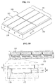
- FIGS. 1A and 1B illustrate an example of a structure of a multi-array ultrasonic probe apparatus 100.
- FIG. 1A is a perspective view of the multi-array ultrasonic probe apparatus 100
- FIG. 1B is a cross-sectional view cut along a line A-A' of FIG. 1A .
- the multi-array ultrasonic probe apparatus 100 includes a tile 101, and a substrate 103.
- n tiles 98 may be provided.
- n denotes a natural number.
- FIG. 1A illustrates only eight tiles, any appropriate number of tiles, fewer or greater than eight, may be provided.
- the tile 101 may obtain ultrasonic data by transmitting and receiving an ultrasonic beam with respect to a target object.
- the tile 101 may include an Application Specific Integrated Circuit (ASIC), and a Capacitive Micromachined Ultrasonic Transducer (CMUT) attached on an upper portion of the ASIC.
- ASIC Application Specific Integrated Circuit
- CMUT Capacitive Micromachined Ultrasonic Transducer
- the substrate 103 includes n guide portions 105 and n adhesive portions 107 which correspond to n tiles 98 and are provided in a form of a matrix.
- the n tiles 98 may be mounted on the n guide portions 105 and may be aligned in a form of a multi-array, which may include a multiple number of one-dimensional arrays. That is, the n guide portions 105 may be attached in rows and columns on the substrate 103 such that a predetermined gap separates the n guide portions 105. Also, the n adhesive portions 107 may be arranged in rows and columns on the substrate 103 such that a predetermined gap separates the n adhesive portions 107. Accordingly, the n tiles 98 may be aligned in uniform directions, by disposing the n tiles 98 to be mounted on the n guide portions 105 collinearly, for example, in an x-axial direction or a y-axial direction.
- the n guide portions 105 may be provided on an upper surface 150 of the substrate 103 so that the n tiles 98 may be mounted on the n guide portions 105, respectively.
- the n adhesive portions 107 may be provided on a lower surface 152 of the substrate 103 at positions corresponding to the positions of the n guide portions 105, respectively.
- An adhesive material for example epoxy, may be disposed in the adhesive portions 107 to bond the n tiles 98 to the substrate 103.
- the substrate 103 may include an outlet 109 on one side of one or more of the adhesive portions 107. Accordingly, when the adhesive material, disposed in the respective adhesive portion 107 is pressed by the tile 101 to be mounted in the respective guide portion 105, the adhesive material may be prevented from leaking in a direction of the tile 101 by discharging the adhesive material to an outside through the respective outlet 109, thereby preventing damage to the tile 101.
- FIG. 2 illustrates an example of a multi-array ultrasonic probe apparatus 200.
- an uppermost diagram is a top view of the multi-array ultrasonic probe apparatus 200
- a lowermost diagram is a cross-sectional view cut along a line B-B'.
- the multi-array ultrasonic probe apparatus 200 includes a tile 201, and a substrate 203.
- n tiles 198 may be provided.
- n denotes a natural number.
- the tile 201 may transmit and receive an ultrasonic beam with respect to a target object.
- the tile 201 includes an ASIC 201-1, with a lower portion 260 disposed on a corresponding adhesive portion 207, and a CMUT 201-2 disposed on an upper portion 262 of the ASIC 201-1.
- the CMUT 201-2 may be attached to the ASIC 201-1 by flip chip bonding technology.
- the substrate 203 may be formed of silicon, glass, or a polymer-based material.
- the substrate 203 includes guide portions 205 and adhesive portions 207, which correspond to n tiles 198.
- An outlet or outlets 209 may be disposed on one or both sides of one or more of the adhesive portions 205.
- the substrate 203 may be formed by semiconductor process technology or imprinting technology.
- a margin of error of the guide portion 205 and the adhesive portion 207 may be reduced to be within a few micrometers ( ⁇ m). Accordingly, the tiles 198 to be mounted in the respective guide portions 205 and to be in contact with adhesive portions 207 may be aligned uniformly.
- the substrate 203 is formed of the polymer-based material by the imprinting technology using a preformed substrate, for example a silicon substrate. Accordingly, the substrate 203 may be formed at a relatively low cost or in a relatively short period of time.
- the n guide portions 205 corresponding to a number of the tiles 198 may be provided.
- the n tiles 198 may be mounted on the n guide portions 205, respectively, to be aligned in a form of a multi-array.
- the respective guide portion 205 may be provided in a shape identical to an outline of the tile 201 so that the tile 201 may be readily inserted and mounted on the guide portion 205.
- the guide portion 205 may be formed to have inner corners provided at right angles, for example, in an L-shape and a mirrored L-shape. Accordingly, the tile 201 may be mounted in the guide portion 205 such that a portion of a lower end of the tile 201, and a portion of a side of the tile 201 may be in contact with the guide portion 205, simultaneously.
- the guide portion 205 by forming the guide portion 205 to have a width w1 wider than a width w2 of the tile 201. by a predetermined size, for example, 10 to 20 micrometers ( ⁇ m), the tile 201 may be readily inserted in the guide portion 205.
- the tile 201 may be mounted in a central portion of the guide portion 205 such that a predetermined gap 250 may be maintained on both sides of the tile 201.
- a 5 ⁇ m gap may be maintained on a left side between the guide portion 205 and one side of the tile 201, and a 5 ⁇ m gap may be maintained on a right side between the guide portion 205 and another side of the tile 201, as seen in a lower part of FIG. 2 .
- the adhesive portion 207 may be formed on or proximate to a lower portion of the respective guide portion 205, and an adhesive material, for example epoxy, may be disposed in the adhesive portion 207 to bond the tile 201 to the substrate 203.
- an adhesive material for example epoxy
- the n guide portions 205 may be disposed in a form of a matrix on the substrate 203 such that a predetermined gap, for example, a 20 ⁇ m gap, separates the n guide portions from one another.
- the n adhesive portions 207 may be disposed in a form of a matrix on the substrate 203 such that a predetermined gap, for example, a 20 ⁇ m gap, separates the n adhesive portions 207 from one another.
- the n tiles 198 to be mounted in the guide portions 205, respectively, may be disposed collinearly, for example, in an x-axial direction or a y-axial direction, whereby the n tiles 198 may be aligned in uniform directions.
- the directions of the n tiles 198 may be aligned by the n guide portions 205 and the n adhesive portions 207. Accordingly, a direction for transmitting and receiving an ultrasonic beam at the tiles 198 may be controlled, whereby an accuracy of the ultrasonic beam may be increased.
- the guide portion 205 may be formed to have a width wider than a width of the corresponding adhesive portion 207 so that the tile 201 may be in contact with the adhesive portion 207 disposed in a lower portion of the guide portion 205, and a portion in which the tile 201 may be mounted stably may be secured.
- the n guide portions 205 may each have identical heights h1, and the n adhesive portions 207 may each have identical heights h2.
- the n guide portions 205 may each be formed to have identical heights in a range of tens of ⁇ m to hundreds of ⁇ m.
- the n adhesive portions 207 each may be formed to have identical heights in a range of tens of ⁇ m to hundreds of ⁇ m.
- each of the n guide portions 205 is formed to have identical heights
- each of the n adhesive portions 207 is formed to have identical heights
- the tiles 198 may be mounted on the substrate 203 at identical heights, whereby even leveling of the tiles 198 may be supported and provided. Accordingly, the n guide portions 205 and the n adhesive portions 207 may enable the leveling of the tiles 198 such that a time for transmitting and receiving the ultrasonic beam at the n tiles 198 may be controlled, for example, identically.
- the n guide portions 205 and the n adhesive portions 207 may enable the n tiles 198 to have identical heights. Accordingly, when each of the tiles 198 transmits an ultrasonic beam to a target object at identical times, and a feedback ultrasonic beam arrives from the target object at identical times, the feedback ultrasonic beam may be received or detected at identical times.
- the heights of the guide portions 205 or the heights of the adhesive portions 207 may be identical or different.
- At least one of the adhesive portions 207 may include a first projection 207-1, for example, a column-shaped projection, to reduce a movement of the adhesive portion 207 resulting from oscillation of the corresponding tile 201 occurring during transmission and reception of an ultrasonic beam, thereby bonding the tile 201 to the substrate 203 more stably.
- a first projection 207-1 for example, a column-shaped projection, to reduce a movement of the adhesive portion 207 resulting from oscillation of the corresponding tile 201 occurring during transmission and reception of an ultrasonic beam, thereby bonding the tile 201 to the substrate 203 more stably.
- two first projections 207-1 are formed, but this is not limiting and any appropriate number of projections may be formed.
- Outlets 209 may be provided on one side or both sides of the n adhesive portions 207.
- the adhesive material disposed in the respective adhesive portion 207 is pressed by the tile 201 to be mounted in the guide portion 205, the adhesive material may be discharged to an outside. That is, when the tile 201 is inserted in the respective guide portion 205, the outlet 209 may provide a path for discharging the adhesive material disposed in the respective adhesive portion 207 to the outside of the structure, thereby preventing the adhesive material from leaking to the tile 201 to prevent a malfunction of the tile 201.
- the substrate 203 further includes a second projection 211 which is disposed between the adjacent guide portions 205 and has sides proximate to adjacent guide portions 205, respectively, to separate the adjacent guide portions 205.
- the second projection 211 may be formed to have, for example, a height and a width in a range of tens of ⁇ m.
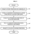
- FIG. 3 illustrates an example of a method of manufacturing a multi-array ultrasonic probe apparatus.
- n guide portions are formed, on a substrate, to mount n tiles, respectively.
- the substrate may include a polymer substrate, a Silicon-on-Insulator (SOI) substrate, a substrate formed of at least one semiconductor material including silicon (Si), germanium (Ge), silicon germanium (SiGe), gallium phosphide (GaP), gallium arsenide (GaAs,) silicon carbide (SiC), silicon germanium carbide (SiGeC), indium arsenide (InAs), and indium phosphide (InP), and the like.
- the semiconductor material is not limited thereto.
- the n guide portions may be disposed in a form of a matrix on the substrate such that a predetermined gap, for example, a 20 ⁇ m gap, separates the n guide portions. That is, the n guide portions may enable the n tiles to be disposed collinearly, for example, in an x-axial direction or a y-axial direction, so that the n tiles may be aligned in uniform directions. Accordingly, a direction for transmitting and receiving an ultrasonic beam at the tiles may be controlled, whereby an accuracy of the ultrasonic beam may be increased.
- a predetermined gap for example, a 20 ⁇ m gap
- n guide portions When the n guide portions are formed to have identical heights in the range of tens of ⁇ m to hundreds of ⁇ m, leveling of the n tiles to be mounted in the n guide portions may be supported.
- a guide portion may be formed to have a width wider than a width of a tile by a predetermined size, for example, 10 ⁇ m to 20 ⁇ m, whereby the tile may be readily inserted.
- a second projection for example, a column-shaped projection
- the second projection may correspond to a portion remaining between the adjacent guide portions, without being etched, during a process of forming the n guide portions, for example, by an etching process.
- the second projection may be formed to have a height and a width of tens of ⁇ m.
- n adhesive portions are formed in a lower portion of the guide portions.
- An adhesive material for example epoxy, may be disposed in the n adhesive portions to bond the n tiles to the substrate.
- the n adhesive portions may be disposed in a form of a matrix in the lower portion of the guide portions, at positions corresponding to positions of the n guide portions.
- the n adhesive portions may be formed to have identical heights in the range of tens of ⁇ m to hundreds of ⁇ m.
- An adhesive portion may be formed to have a width narrower than a width of a guide portion by a predetermined size such that a tile to be mounted in the guide portion may be in contact with the adhesive portion while a gap for mounting the tile stably may be secured in the guide portion.
- the adhesive portion may include a first projection, for example, a column-shaped projection, thereby reducing a movement of the adhesive portion resulting from oscillation generated by the tile to be mounted in the guide portion and to be in contact with the adhesive portion during transmission and reception of an ultrasonic beam. Accordingly, the tile may be bonded to the substrate more stably.
- n outlets are formed, on one side of the n adhesive portions, to discharge the adhesive material to be disposed in the adhesive portion to an outside.
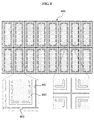
- the substrate may be formed, as shown in FIG. 4 .
- the outlets are formed on one side of the adhesive portions, the positions of the outlets are not limited thereto.
- the outlets may be formed on both sides facing each other, whereby the adhesive material may be discharged to the outside on both sides.
- the substrate 400 includes n guide portions 401, n adhesive portions 403, and n outlets 405.
- the n adhesive portions are filled with the adhesive material, for example, epoxy.
- the n tiles are inserted in the n guide portions, respectively.
- the n tiles may be mounted on the substrate, as shown in FIG. 5 .
- An individual tile may correspond to a chip on which an ASIC and a CMUT may be laminated sequentially.
- a multi-array ultrasonic probe apparatus may be formed by mounting n tiles 503 on a substrate 501, sequentially.
- the outlets formed on one side of the adhesive portions may discharge the adhesive material to an outside when the adhesive material is pressed by the tiles to be mounted in the guide portions and simultaneously, to be in contact with the adhesive material disposed in the adhesive portions disposed in a lower portion of the guide portions. That is, an outlet may provide a path for discharging the adhesive material to the outside when the tiles are mounted in the guide portion, thereby preventing the adhesive material from leaking to the tile, and preventing damage to the tile.
- FIG. 6 illustrates an example of a method of manufacturing a substrate of a multi-array ultrasonic probe apparatus.
- a substrate is provided.
- the substrate may be formed of silicon, or glass.
- a first photo resist (PR) pattern 650 is formed on the substrate.
- the first PR pattern may define a first hole 652 in which a tile may be disposed.
- the first hole is formed by etching the substrate using the first PR pattern as an etching mask.
- a height of the first hole may be controlled by etching the substrate to a depth in the range of tens of ⁇ m to hundreds of ⁇ m.
- a plurality of first holes may be formed in rows and columns to be separated from each other by a predetermined gap.
- the plurality of first holes may be formed collinearly, in an x-axial direction or a y-axial direction. Accordingly, a plurality of tiles to be fixed in the plurality of holes may be aligned in uniform directions.
- the first hole may be formed to have a width wider than a width of the tile by a predetermined size, for example, 10 ⁇ m to 20 ⁇ m, whereby the tile may be readily inserted.
- a second projection for example, in a column-shaped projection, may be formed, on the substrate, to separate adjacent first holes. That is, the second projection may refer to a portion remaining between the adjacent first holes, without being etched by the first PR pattern, during a process of forming the first holes on the substrate through an etching process.
- a second PR pattern 660 is formed on the first hole.
- the second PR pattern may define a second hole 662 in which an adhesive material may be disposed.
- the second hole is formed by etching a portion of the first hole using the second PR pattern as an etching mask. For instance, a height of the second hole may be controlled by etching the first hole to a depth in the range of tens of ⁇ m to hundreds of ⁇ m.
- a plurality of second holes may be formed in a lower portion of the plurality of first holes forming a ledge 664 corresponding to a lower portion of the guide portion.
- the ledge may be formed to extend continually around the perimeter of the second hole 662 or may be formed to extend from the opposite sides of the first hole 652, forming two ledges.
- the configuration of the ledge is not limited thereto.
- the plurality of second holes may also be formed in rows and columns to be separated from each other by a predetermined gap.
- the first PR pattern and the second PR pattern are eliminated.
- the elimination of the first PR pattern and the second PR pattern may be performed using a method generally known in the art, for example, an ashing process using gas plasma, for example, oxygen gas (O 2 ), nitrogen gas (N 2 ), hydrogen gas (H 2 ), and the like.
- gas plasma for example, oxygen gas (O 2 ), nitrogen gas (N 2 ), hydrogen gas (H 2 ), and the like.
- the first hole, that is, the guide portion, and the second hole, that is, the adhesive portion may be formed on the substrate, by controlling a size of the first hole and a size of the second hole adroitly in units of ⁇ m.
- the size of the first hole and the size of the second hole may include, for example, a height, and a width.
- the plurality of first holes and the plurality of second holes may be provided in a form of a matrix including rows and columns, whereby the substrate on which tiles may be aligned in a form of a multi-array may be formed.
- FIG. 7 illustrates another example of a method of manufacturing a substrate of a multi-array ultrasonic probe apparatus.
- a first substrate 748 including a guide portion 750 and an adhesive portion 752 is provided.
- the first substrate may refer to a substrate formed by the operations of FIG. 6 .
- the substrate may be formed of silicon, or glass.
- an oxidized layer 754 is formed by oxidation of a surface of the first substrate 748. Operation 703 may be omitted selectively.
- a stamp frame 760 is formed by forming an electroplating layer on the first substrate.
- a second substrate 762 having an identical shape of the first substrate is formed, by performing imprinting on the second substrate that is formed of a polymer-based material, using the stamp frame as an imprinting jig.
- the substrate may be formed at a relatively low cost or in a relatively short period of time by forming the substrate using imprinting technology, when compared to a substrate formed using the semiconductor process technology.
Landscapes
- Engineering & Computer Science (AREA)
- Physics & Mathematics (AREA)
- Acoustics & Sound (AREA)
- Health & Medical Sciences (AREA)
- Life Sciences & Earth Sciences (AREA)
- Signal Processing (AREA)
- Mechanical Engineering (AREA)
- Multimedia (AREA)
- General Health & Medical Sciences (AREA)
- Pathology (AREA)
- Manufacturing & Machinery (AREA)
- Nuclear Medicine, Radiotherapy & Molecular Imaging (AREA)
- Chemical & Material Sciences (AREA)
- Animal Behavior & Ethology (AREA)
- Biomedical Technology (AREA)
- Public Health (AREA)
- Veterinary Medicine (AREA)
- Radiology & Medical Imaging (AREA)
- Molecular Biology (AREA)
- Heart & Thoracic Surgery (AREA)
- Surgery (AREA)
- Analytical Chemistry (AREA)
- Biochemistry (AREA)
- General Physics & Mathematics (AREA)
- Immunology (AREA)
- Biophysics (AREA)
- Medical Informatics (AREA)
- Transducers For Ultrasonic Waves (AREA)
- Ultra Sonic Daignosis Equipment (AREA)
- Investigating Or Analyzing Materials By The Use Of Ultrasonic Waves (AREA)
Applications Claiming Priority (1)
| Application Number | Priority Date | Filing Date | Title |
|---|---|---|---|
| KR1020120026098A KR101378012B1 (ko) | 2012-03-14 | 2012-03-14 | 멀티 어레이형 초음파 프로브 장치 및 멀티 어레이형 초음파 프로브 장치의 제조 방법 |
Publications (3)
| Publication Number | Publication Date |
|---|---|
| EP2639789A2 EP2639789A2 (en) | 2013-09-18 |
| EP2639789A3 EP2639789A3 (en) | 2014-02-26 |
| EP2639789B1 true EP2639789B1 (en) | 2016-06-08 |
Family
ID=47913010
Family Applications (1)
| Application Number | Title | Priority Date | Filing Date |
|---|---|---|---|
| EP13159231.3A Active EP2639789B1 (en) | 2012-03-14 | 2013-03-14 | Multi-array ultrasonic probe apparatus and method for manufacturing multi-array probe apparatus |
Country Status (5)
| Country | Link |
|---|---|
| US (1) | US9071893B2 (https=) |
| EP (1) | EP2639789B1 (https=) |
| JP (1) | JP5666640B2 (https=) |
| KR (1) | KR101378012B1 (https=) |
| CN (1) | CN103300882B (https=) |
Families Citing this family (7)
| Publication number | Priority date | Publication date | Assignee | Title |
|---|---|---|---|---|
| EP3370621B1 (en) * | 2015-11-02 | 2019-01-09 | Koninklijke Philips N.V. | Ultrasound transducer array, probe and system |
| WO2017211754A1 (en) * | 2016-06-09 | 2017-12-14 | Koninklijke Philips N.V. | Coolable ultrasound probe |
| JP6712917B2 (ja) * | 2016-07-14 | 2020-06-24 | 株式会社日立製作所 | 半導体センサチップアレイ、および超音波診断装置 |
| WO2018060456A1 (en) * | 2016-09-29 | 2018-04-05 | Koninklijke Philips N.V. | Ultrasound system, method and computer program product |
| KR101915255B1 (ko) * | 2017-01-11 | 2018-11-05 | 삼성메디슨 주식회사 | 초음파 프로브의 제조 방법 및 그 초음파 프로브 |
| CN115398183A (zh) * | 2020-01-17 | 2022-11-25 | 大不列颠哥伦比亚大学 | 柔性电容式微加工超声换能器阵列 |
| KR102492901B1 (ko) * | 2021-03-31 | 2023-01-30 | 국방과학연구소 | 압전단결정 복합체 음향센서 및 이를 포함하는 배열 음향센서 |
Family Cites Families (27)
| Publication number | Priority date | Publication date | Assignee | Title |
|---|---|---|---|---|
| EP0427052B1 (de) * | 1989-11-09 | 1993-03-31 | Oerlikon-Contraves AG | Verfahren zur Herstellung von Hybridschaltungen mit einem Array aus gleichen elektronischen Elementen |
| JP3131485B2 (ja) | 1992-02-04 | 2001-01-31 | オリンパス光学工業株式会社 | 超音波プローブ |
| JP3535204B2 (ja) | 1994-02-28 | 2004-06-07 | 株式会社東芝 | 超音波プローブ及びその製造方法 |
| US5655276A (en) | 1995-02-06 | 1997-08-12 | General Electric Company | Method of manufacturing two-dimensional array ultrasonic transducers |
| US6043590A (en) | 1997-04-18 | 2000-03-28 | Atl Ultrasound | Composite transducer with connective backing block |
| JP4723732B2 (ja) * | 2000-07-12 | 2011-07-13 | セイコーインスツル株式会社 | 脈検出装置及び超音波診断装置 |
| JP3449345B2 (ja) | 2000-08-11 | 2003-09-22 | 株式会社村田製作所 | センサアレイおよび送受信装置 |
| JP4562106B2 (ja) * | 2000-11-27 | 2010-10-13 | セイコーインスツル株式会社 | 超音波診断装置 |
| KR100684677B1 (ko) | 2002-06-05 | 2007-02-23 | 야마이치덴키 가부시키가이샤 | 프로브 유닛 및 그 제조 방법 |
| US7280435B2 (en) | 2003-03-06 | 2007-10-09 | General Electric Company | Switching circuitry for reconfigurable arrays of sensor elements |
| JP4261298B2 (ja) | 2003-09-19 | 2009-04-30 | 富士フイルム株式会社 | 積層構造体アレイ及びその製造方法、並びに、超音波トランスデューサアレイの製造方法 |
| GB2430259B (en) | 2004-01-08 | 2007-07-25 | Schlumberger Holdings | Integrated Acoustic Transducer Assembly |
| JP2005342337A (ja) * | 2004-06-04 | 2005-12-15 | Matsushita Electric Ind Co Ltd | 超音波探触子 |
| KR20070083514A (ko) | 2004-07-28 | 2007-08-24 | 에스브이 프로브 피티이 엘티디 | 동일 평면상에 있는 접착 패드를 기판에 형성하는 방법과장치 |
| US7459795B2 (en) | 2004-08-19 | 2008-12-02 | Formfactor, Inc. | Method to build a wirebond probe card in a many at a time fashion |
| US20070152685A1 (en) | 2006-01-03 | 2007-07-05 | Formfactor, Inc. | A probe array structure and a method of making a probe array structure |
| JP5038808B2 (ja) * | 2007-08-02 | 2012-10-03 | 株式会社東芝 | 超音波トランスデューサおよび超音波トランスデューサを備えた超音波プローブ |
| WO2009073692A1 (en) * | 2007-12-03 | 2009-06-11 | Kolo Technologies, Inc. | Packaging and connecting electrostatic transducer arrays |
| KR100967024B1 (ko) | 2008-04-14 | 2010-06-30 | 삼성전기주식회사 | 프로브 기판 제조 방법 |
| KR100996150B1 (ko) | 2008-05-23 | 2010-11-24 | 주식회사 엠아이티 | 프로브핀의 정열판과 통전판 및 그의 기판 제조방법 |
| JP2010022931A (ja) | 2008-07-18 | 2010-02-04 | Fujifilm Corp | 接着剤はみ出し防止構造を有する超音波探触子 |
| KR101137262B1 (ko) | 2009-03-18 | 2012-04-20 | 삼성메디슨 주식회사 | 초음파 진단장치용 프로브 및 그 제조방법 |
| US8345508B2 (en) | 2009-09-20 | 2013-01-01 | General Electric Company | Large area modular sensor array assembly and method for making the same |
| JP5462735B2 (ja) | 2010-07-01 | 2014-04-02 | 日立アロカメディカル株式会社 | 超音波探触子の製造方法、および、超音波探触子 |
| US20120029393A1 (en) * | 2010-07-30 | 2012-02-02 | General Electric Company | Compact ultrasound transducer assembly and methods of making and using the same |
| US8776335B2 (en) | 2010-11-17 | 2014-07-15 | General Electric Company | Methods of fabricating ultrasonic transducer assemblies |
| KR101354603B1 (ko) | 2012-01-02 | 2014-01-23 | 삼성메디슨 주식회사 | 초음파 프로브 및 그 제조방법 |
-
2012
- 2012-03-14 KR KR1020120026098A patent/KR101378012B1/ko active Active
-
2013
- 2013-01-15 US US13/741,907 patent/US9071893B2/en active Active
- 2013-03-12 CN CN201310077389.5A patent/CN103300882B/zh active Active
- 2013-03-13 JP JP2013049912A patent/JP5666640B2/ja active Active
- 2013-03-14 EP EP13159231.3A patent/EP2639789B1/en active Active
Also Published As
| Publication number | Publication date |
|---|---|
| US20130242705A1 (en) | 2013-09-19 |
| US9071893B2 (en) | 2015-06-30 |
| CN103300882B (zh) | 2016-03-30 |
| KR101378012B1 (ko) | 2014-03-24 |
| EP2639789A3 (en) | 2014-02-26 |
| JP2013192228A (ja) | 2013-09-26 |
| KR20130104531A (ko) | 2013-09-25 |
| JP5666640B2 (ja) | 2015-02-12 |
| EP2639789A2 (en) | 2013-09-18 |
| CN103300882A (zh) | 2013-09-18 |
Similar Documents
| Publication | Publication Date | Title |
|---|---|---|
| EP2639789B1 (en) | Multi-array ultrasonic probe apparatus and method for manufacturing multi-array probe apparatus | |
| US7795784B2 (en) | Redistribution interconnect for microbeamforming(s) and a medical ultrasound system | |
| US7249509B2 (en) | Angular velocity detector | |
| US10531860B2 (en) | High frequency ultrasound transducer and method for manufacture | |
| US8776335B2 (en) | Methods of fabricating ultrasonic transducer assemblies | |
| EP2246292B1 (en) | Package interface plate for mechanical isolation of MEMS structures | |
| US20140069194A1 (en) | Ultrasonic transducers | |
| US9136139B2 (en) | Jig, manufacturing method thereof, and flip chip bonding method for chips of ultrasound probe using jig | |
| US12558708B2 (en) | Array architecture and interconnection for transducers | |
| KR102078870B1 (ko) | 초음파 변환기 | |
| CN116075369B (zh) | 超声换能器和超声换能器的平铺阵列 | |
| KR20160023156A (ko) | 전자소자의 패키징 시스템 및 패키징 방법 | |
| US8814326B2 (en) | Reduced mechanical coupling with structured flex circuits | |
| EP4149692B1 (en) | An ultrasound transducer and a tiled array of ultrasound transducers | |
| WO2012085724A1 (en) | Method of fabricating a flip chip electrical coupling, a flip chip electrical coupling, and a device comprising a flip chip electrical coupling | |
| IT202200024411A1 (it) | Dispositivo trasduttore mems per applicazioni ad alta frequenza, e metodo di fabbricazione | |
| IT202300005940A1 (it) | Metodo di fabbricazione di un dispositivo trasduttore mems con membrana sottile, e dispositivo trasduttore mems | |
| CN118083901A (zh) | 用于高频应用的mems换能器器件以及制造方法 |
Legal Events
| Date | Code | Title | Description |
|---|---|---|---|
| PUAI | Public reference made under article 153(3) epc to a published international application that has entered the european phase |
Free format text: ORIGINAL CODE: 0009012 |
|
| AK | Designated contracting states |
Kind code of ref document: A2 Designated state(s): AL AT BE BG CH CY CZ DE DK EE ES FI FR GB GR HR HU IE IS IT LI LT LU LV MC MK MT NL NO PL PT RO RS SE SI SK SM TR |
|
| AX | Request for extension of the european patent |
Extension state: BA ME |
|
| PUAL | Search report despatched |
Free format text: ORIGINAL CODE: 0009013 |
|
| AK | Designated contracting states |
Kind code of ref document: A3 Designated state(s): AL AT BE BG CH CY CZ DE DK EE ES FI FR GB GR HR HU IE IS IT LI LT LU LV MC MK MT NL NO PL PT RO RS SE SI SK SM TR |
|
| AX | Request for extension of the european patent |
Extension state: BA ME |
|
| RIC1 | Information provided on ipc code assigned before grant |
Ipc: G10K 11/00 20060101AFI20140121BHEP Ipc: B06B 1/02 20060101ALI20140121BHEP |
|
| 17P | Request for examination filed |
Effective date: 20140327 |
|
| RBV | Designated contracting states (corrected) |
Designated state(s): AL AT BE BG CH CY CZ DE DK EE ES FI FR GB GR HR HU IE IS IT LI LT LU LV MC MK MT NL NO PL PT RO RS SE SI SK SM TR |
|
| 17Q | First examination report despatched |
Effective date: 20150507 |
|
| GRAP | Despatch of communication of intention to grant a patent |
Free format text: ORIGINAL CODE: EPIDOSNIGR1 |
|
| INTG | Intention to grant announced |
Effective date: 20160108 |
|
| GRAS | Grant fee paid |
Free format text: ORIGINAL CODE: EPIDOSNIGR3 |
|
| GRAA | (expected) grant |
Free format text: ORIGINAL CODE: 0009210 |
|
| AK | Designated contracting states |
Kind code of ref document: B1 Designated state(s): AL AT BE BG CH CY CZ DE DK EE ES FI FR GB GR HR HU IE IS IT LI LT LU LV MC MK MT NL NO PL PT RO RS SE SI SK SM TR |
|
| REG | Reference to a national code |
Ref country code: GB Ref legal event code: FG4D |
|
| REG | Reference to a national code |
Ref country code: CH Ref legal event code: EP |
|
| REG | Reference to a national code |
Ref country code: IE Ref legal event code: FG4D |
|
| REG | Reference to a national code |
Ref country code: AT Ref legal event code: REF Ref document number: 805727 Country of ref document: AT Kind code of ref document: T Effective date: 20160715 |
|
| REG | Reference to a national code |
Ref country code: DE Ref legal event code: R096 Ref document number: 602013008311 Country of ref document: DE |
|
| REG | Reference to a national code |
Ref country code: LT Ref legal event code: MG4D |
|
| REG | Reference to a national code |
Ref country code: NL Ref legal event code: MP Effective date: 20160608 |
|
| PG25 | Lapsed in a contracting state [announced via postgrant information from national office to epo] |
Ref country code: FI Free format text: LAPSE BECAUSE OF FAILURE TO SUBMIT A TRANSLATION OF THE DESCRIPTION OR TO PAY THE FEE WITHIN THE PRESCRIBED TIME-LIMIT Effective date: 20160608 Ref country code: NO Free format text: LAPSE BECAUSE OF FAILURE TO SUBMIT A TRANSLATION OF THE DESCRIPTION OR TO PAY THE FEE WITHIN THE PRESCRIBED TIME-LIMIT Effective date: 20160908 Ref country code: LT Free format text: LAPSE BECAUSE OF FAILURE TO SUBMIT A TRANSLATION OF THE DESCRIPTION OR TO PAY THE FEE WITHIN THE PRESCRIBED TIME-LIMIT Effective date: 20160608 |
|
| REG | Reference to a national code |
Ref country code: AT Ref legal event code: MK05 Ref document number: 805727 Country of ref document: AT Kind code of ref document: T Effective date: 20160608 |
|
| PG25 | Lapsed in a contracting state [announced via postgrant information from national office to epo] |
Ref country code: RS Free format text: LAPSE BECAUSE OF FAILURE TO SUBMIT A TRANSLATION OF THE DESCRIPTION OR TO PAY THE FEE WITHIN THE PRESCRIBED TIME-LIMIT Effective date: 20160608 Ref country code: LV Free format text: LAPSE BECAUSE OF FAILURE TO SUBMIT A TRANSLATION OF THE DESCRIPTION OR TO PAY THE FEE WITHIN THE PRESCRIBED TIME-LIMIT Effective date: 20160608 Ref country code: HR Free format text: LAPSE BECAUSE OF FAILURE TO SUBMIT A TRANSLATION OF THE DESCRIPTION OR TO PAY THE FEE WITHIN THE PRESCRIBED TIME-LIMIT Effective date: 20160608 Ref country code: GR Free format text: LAPSE BECAUSE OF FAILURE TO SUBMIT A TRANSLATION OF THE DESCRIPTION OR TO PAY THE FEE WITHIN THE PRESCRIBED TIME-LIMIT Effective date: 20160909 Ref country code: SE Free format text: LAPSE BECAUSE OF FAILURE TO SUBMIT A TRANSLATION OF THE DESCRIPTION OR TO PAY THE FEE WITHIN THE PRESCRIBED TIME-LIMIT Effective date: 20160608 Ref country code: NL Free format text: LAPSE BECAUSE OF FAILURE TO SUBMIT A TRANSLATION OF THE DESCRIPTION OR TO PAY THE FEE WITHIN THE PRESCRIBED TIME-LIMIT Effective date: 20160608 Ref country code: ES Free format text: LAPSE BECAUSE OF FAILURE TO SUBMIT A TRANSLATION OF THE DESCRIPTION OR TO PAY THE FEE WITHIN THE PRESCRIBED TIME-LIMIT Effective date: 20160608 |
|
| PG25 | Lapsed in a contracting state [announced via postgrant information from national office to epo] |
Ref country code: IT Free format text: LAPSE BECAUSE OF FAILURE TO SUBMIT A TRANSLATION OF THE DESCRIPTION OR TO PAY THE FEE WITHIN THE PRESCRIBED TIME-LIMIT Effective date: 20160608 Ref country code: RO Free format text: LAPSE BECAUSE OF FAILURE TO SUBMIT A TRANSLATION OF THE DESCRIPTION OR TO PAY THE FEE WITHIN THE PRESCRIBED TIME-LIMIT Effective date: 20160608 Ref country code: IS Free format text: LAPSE BECAUSE OF FAILURE TO SUBMIT A TRANSLATION OF THE DESCRIPTION OR TO PAY THE FEE WITHIN THE PRESCRIBED TIME-LIMIT Effective date: 20161008 Ref country code: SK Free format text: LAPSE BECAUSE OF FAILURE TO SUBMIT A TRANSLATION OF THE DESCRIPTION OR TO PAY THE FEE WITHIN THE PRESCRIBED TIME-LIMIT Effective date: 20160608 Ref country code: CZ Free format text: LAPSE BECAUSE OF FAILURE TO SUBMIT A TRANSLATION OF THE DESCRIPTION OR TO PAY THE FEE WITHIN THE PRESCRIBED TIME-LIMIT Effective date: 20160608 Ref country code: EE Free format text: LAPSE BECAUSE OF FAILURE TO SUBMIT A TRANSLATION OF THE DESCRIPTION OR TO PAY THE FEE WITHIN THE PRESCRIBED TIME-LIMIT Effective date: 20160608 |
|
| PG25 | Lapsed in a contracting state [announced via postgrant information from national office to epo] |
Ref country code: PL Free format text: LAPSE BECAUSE OF FAILURE TO SUBMIT A TRANSLATION OF THE DESCRIPTION OR TO PAY THE FEE WITHIN THE PRESCRIBED TIME-LIMIT Effective date: 20160608 Ref country code: PT Free format text: LAPSE BECAUSE OF FAILURE TO SUBMIT A TRANSLATION OF THE DESCRIPTION OR TO PAY THE FEE WITHIN THE PRESCRIBED TIME-LIMIT Effective date: 20161010 Ref country code: BE Free format text: LAPSE BECAUSE OF FAILURE TO SUBMIT A TRANSLATION OF THE DESCRIPTION OR TO PAY THE FEE WITHIN THE PRESCRIBED TIME-LIMIT Effective date: 20160608 Ref country code: SM Free format text: LAPSE BECAUSE OF FAILURE TO SUBMIT A TRANSLATION OF THE DESCRIPTION OR TO PAY THE FEE WITHIN THE PRESCRIBED TIME-LIMIT Effective date: 20160608 Ref country code: AT Free format text: LAPSE BECAUSE OF FAILURE TO SUBMIT A TRANSLATION OF THE DESCRIPTION OR TO PAY THE FEE WITHIN THE PRESCRIBED TIME-LIMIT Effective date: 20160608 |
|
| REG | Reference to a national code |
Ref country code: DE Ref legal event code: R097 Ref document number: 602013008311 Country of ref document: DE |
|
| PLBE | No opposition filed within time limit |
Free format text: ORIGINAL CODE: 0009261 |
|
| STAA | Information on the status of an ep patent application or granted ep patent |
Free format text: STATUS: NO OPPOSITION FILED WITHIN TIME LIMIT |
|
| 26N | No opposition filed |
Effective date: 20170309 |
|
| PG25 | Lapsed in a contracting state [announced via postgrant information from national office to epo] |
Ref country code: SI Free format text: LAPSE BECAUSE OF FAILURE TO SUBMIT A TRANSLATION OF THE DESCRIPTION OR TO PAY THE FEE WITHIN THE PRESCRIBED TIME-LIMIT Effective date: 20160608 Ref country code: DK Free format text: LAPSE BECAUSE OF FAILURE TO SUBMIT A TRANSLATION OF THE DESCRIPTION OR TO PAY THE FEE WITHIN THE PRESCRIBED TIME-LIMIT Effective date: 20160608 |
|
| REG | Reference to a national code |
Ref country code: CH Ref legal event code: PL |
|
| GBPC | Gb: european patent ceased through non-payment of renewal fee |
Effective date: 20170314 |
|
| PG25 | Lapsed in a contracting state [announced via postgrant information from national office to epo] |
Ref country code: MC Free format text: LAPSE BECAUSE OF FAILURE TO SUBMIT A TRANSLATION OF THE DESCRIPTION OR TO PAY THE FEE WITHIN THE PRESCRIBED TIME-LIMIT Effective date: 20160608 |
|
| REG | Reference to a national code |
Ref country code: IE Ref legal event code: MM4A |
|
| REG | Reference to a national code |
Ref country code: FR Ref legal event code: ST Effective date: 20171130 |
|
| PG25 | Lapsed in a contracting state [announced via postgrant information from national office to epo] |
Ref country code: FR Free format text: LAPSE BECAUSE OF NON-PAYMENT OF DUE FEES Effective date: 20170331 Ref country code: LU Free format text: LAPSE BECAUSE OF NON-PAYMENT OF DUE FEES Effective date: 20170314 |
|
| PG25 | Lapsed in a contracting state [announced via postgrant information from national office to epo] |
Ref country code: CH Free format text: LAPSE BECAUSE OF NON-PAYMENT OF DUE FEES Effective date: 20170331 Ref country code: GB Free format text: LAPSE BECAUSE OF NON-PAYMENT OF DUE FEES Effective date: 20170314 Ref country code: LI Free format text: LAPSE BECAUSE OF NON-PAYMENT OF DUE FEES Effective date: 20170331 Ref country code: IE Free format text: LAPSE BECAUSE OF NON-PAYMENT OF DUE FEES Effective date: 20170314 |
|
| PG25 | Lapsed in a contracting state [announced via postgrant information from national office to epo] |
Ref country code: MT Free format text: LAPSE BECAUSE OF NON-PAYMENT OF DUE FEES Effective date: 20170314 |
|
| PG25 | Lapsed in a contracting state [announced via postgrant information from national office to epo] |
Ref country code: AL Free format text: LAPSE BECAUSE OF FAILURE TO SUBMIT A TRANSLATION OF THE DESCRIPTION OR TO PAY THE FEE WITHIN THE PRESCRIBED TIME-LIMIT Effective date: 20160608 |
|
| PG25 | Lapsed in a contracting state [announced via postgrant information from national office to epo] |
Ref country code: HU Free format text: LAPSE BECAUSE OF FAILURE TO SUBMIT A TRANSLATION OF THE DESCRIPTION OR TO PAY THE FEE WITHIN THE PRESCRIBED TIME-LIMIT; INVALID AB INITIO Effective date: 20130314 |
|
| PG25 | Lapsed in a contracting state [announced via postgrant information from national office to epo] |
Ref country code: BG Free format text: LAPSE BECAUSE OF FAILURE TO SUBMIT A TRANSLATION OF THE DESCRIPTION OR TO PAY THE FEE WITHIN THE PRESCRIBED TIME-LIMIT Effective date: 20160608 |
|
| PG25 | Lapsed in a contracting state [announced via postgrant information from national office to epo] |
Ref country code: CY Free format text: LAPSE BECAUSE OF NON-PAYMENT OF DUE FEES Effective date: 20160608 |
|
| PG25 | Lapsed in a contracting state [announced via postgrant information from national office to epo] |
Ref country code: MK Free format text: LAPSE BECAUSE OF FAILURE TO SUBMIT A TRANSLATION OF THE DESCRIPTION OR TO PAY THE FEE WITHIN THE PRESCRIBED TIME-LIMIT Effective date: 20160608 |
|
| PG25 | Lapsed in a contracting state [announced via postgrant information from national office to epo] |
Ref country code: TR Free format text: LAPSE BECAUSE OF FAILURE TO SUBMIT A TRANSLATION OF THE DESCRIPTION OR TO PAY THE FEE WITHIN THE PRESCRIBED TIME-LIMIT Effective date: 20160608 |
|
| PGFP | Annual fee paid to national office [announced via postgrant information from national office to epo] |
Ref country code: DE Payment date: 20260220 Year of fee payment: 14 |