EP2635948B1 - Verfahren und vorrichtung zur wärmesteuerung von verarbeitungsknoten - Google Patents
Verfahren und vorrichtung zur wärmesteuerung von verarbeitungsknoten Download PDFInfo
- Publication number
- EP2635948B1 EP2635948B1 EP11782700.6A EP11782700A EP2635948B1 EP 2635948 B1 EP2635948 B1 EP 2635948B1 EP 11782700 A EP11782700 A EP 11782700A EP 2635948 B1 EP2635948 B1 EP 2635948B1
- Authority
- EP
- European Patent Office
- Prior art keywords
- frequency
- processing nodes
- limit
- processing
- temperature
- Prior art date
- Legal status (The legal status is an assumption and is not a legal conclusion. Google has not performed a legal analysis and makes no representation as to the accuracy of the status listed.)
- Active
Links
- 238000012545 processing Methods 0.000 title claims description 150
- 238000000034 method Methods 0.000 title claims description 29
- 230000002829 reductive effect Effects 0.000 claims description 20
- 238000013461 design Methods 0.000 claims description 16
- 230000003247 decreasing effect Effects 0.000 claims description 10
- 230000015654 memory Effects 0.000 description 30
- 238000010586 diagram Methods 0.000 description 20
- 230000000670 limiting effect Effects 0.000 description 15
- 230000000694 effects Effects 0.000 description 13
- 238000003860 storage Methods 0.000 description 13
- 230000002093 peripheral effect Effects 0.000 description 10
- 230000009467 reduction Effects 0.000 description 8
- 230000008859 change Effects 0.000 description 6
- 230000006870 function Effects 0.000 description 6
- 230000007423 decrease Effects 0.000 description 4
- 238000012986 modification Methods 0.000 description 4
- 230000004048 modification Effects 0.000 description 4
- 230000009471 action Effects 0.000 description 3
- 230000015572 biosynthetic process Effects 0.000 description 3
- 238000004891 communication Methods 0.000 description 3
- 238000001816 cooling Methods 0.000 description 3
- 238000003786 synthesis reaction Methods 0.000 description 3
- 238000007792 addition Methods 0.000 description 2
- 239000003795 chemical substances by application Substances 0.000 description 2
- 238000009826 distribution Methods 0.000 description 2
- 238000012544 monitoring process Methods 0.000 description 2
- 239000004065 semiconductor Substances 0.000 description 2
- 241000699670 Mus sp. Species 0.000 description 1
- 230000003542 behavioural effect Effects 0.000 description 1
- 230000008901 benefit Effects 0.000 description 1
- 230000001419 dependent effect Effects 0.000 description 1
- 239000004973 liquid crystal related substance Substances 0.000 description 1
- 238000004519 manufacturing process Methods 0.000 description 1
- 230000003287 optical effect Effects 0.000 description 1
- 238000013021 overheating Methods 0.000 description 1
- 230000036961 partial effect Effects 0.000 description 1
- 238000009877 rendering Methods 0.000 description 1
- 230000004044 response Effects 0.000 description 1
- 230000000630 rising effect Effects 0.000 description 1
- 230000003068 static effect Effects 0.000 description 1
- 230000001360 synchronised effect Effects 0.000 description 1
- 238000012546 transfer Methods 0.000 description 1
Images


Classifications
-
- G—PHYSICS
- G06—COMPUTING; CALCULATING OR COUNTING
- G06F—ELECTRIC DIGITAL DATA PROCESSING
- G06F1/00—Details not covered by groups G06F3/00 - G06F13/00 and G06F21/00
- G06F1/16—Constructional details or arrangements
- G06F1/20—Cooling means
- G06F1/206—Cooling means comprising thermal management
-
- G—PHYSICS
- G06—COMPUTING; CALCULATING OR COUNTING
- G06F—ELECTRIC DIGITAL DATA PROCESSING
- G06F1/00—Details not covered by groups G06F3/00 - G06F13/00 and G06F21/00
- G06F1/16—Constructional details or arrangements
- G06F1/20—Cooling means
-
- G—PHYSICS
- G06—COMPUTING; CALCULATING OR COUNTING
- G06F—ELECTRIC DIGITAL DATA PROCESSING
- G06F1/00—Details not covered by groups G06F3/00 - G06F13/00 and G06F21/00
- G06F1/26—Power supply means, e.g. regulation thereof
- G06F1/32—Means for saving power
- G06F1/3203—Power management, i.e. event-based initiation of a power-saving mode
- G06F1/3234—Power saving characterised by the action undertaken
- G06F1/324—Power saving characterised by the action undertaken by lowering clock frequency
-
- G—PHYSICS
- G06—COMPUTING; CALCULATING OR COUNTING
- G06F—ELECTRIC DIGITAL DATA PROCESSING
- G06F1/00—Details not covered by groups G06F3/00 - G06F13/00 and G06F21/00
- G06F1/26—Power supply means, e.g. regulation thereof
- G06F1/32—Means for saving power
- G06F1/3203—Power management, i.e. event-based initiation of a power-saving mode
- G06F1/3234—Power saving characterised by the action undertaken
- G06F1/3296—Power saving characterised by the action undertaken by lowering the supply or operating voltage
-
- Y—GENERAL TAGGING OF NEW TECHNOLOGICAL DEVELOPMENTS; GENERAL TAGGING OF CROSS-SECTIONAL TECHNOLOGIES SPANNING OVER SEVERAL SECTIONS OF THE IPC; TECHNICAL SUBJECTS COVERED BY FORMER USPC CROSS-REFERENCE ART COLLECTIONS [XRACs] AND DIGESTS
- Y02—TECHNOLOGIES OR APPLICATIONS FOR MITIGATION OR ADAPTATION AGAINST CLIMATE CHANGE
- Y02D—CLIMATE CHANGE MITIGATION TECHNOLOGIES IN INFORMATION AND COMMUNICATION TECHNOLOGIES [ICT], I.E. INFORMATION AND COMMUNICATION TECHNOLOGIES AIMING AT THE REDUCTION OF THEIR OWN ENERGY USE
- Y02D10/00—Energy efficient computing, e.g. low power processors, power management or thermal management
-
- Y—GENERAL TAGGING OF NEW TECHNOLOGICAL DEVELOPMENTS; GENERAL TAGGING OF CROSS-SECTIONAL TECHNOLOGIES SPANNING OVER SEVERAL SECTIONS OF THE IPC; TECHNICAL SUBJECTS COVERED BY FORMER USPC CROSS-REFERENCE ART COLLECTIONS [XRACs] AND DIGESTS
- Y02—TECHNOLOGIES OR APPLICATIONS FOR MITIGATION OR ADAPTATION AGAINST CLIMATE CHANGE
- Y02D—CLIMATE CHANGE MITIGATION TECHNOLOGIES IN INFORMATION AND COMMUNICATION TECHNOLOGIES [ICT], I.E. INFORMATION AND COMMUNICATION TECHNOLOGIES AIMING AT THE REDUCTION OF THEIR OWN ENERGY USE
- Y02D30/00—Reducing energy consumption in communication networks
- Y02D30/50—Reducing energy consumption in communication networks in wire-line communication networks, e.g. low power modes or reduced link rate
Definitions
- This invention relates to thermal control of processing nodes.
- a thermal control apparatus in an IC may include one or more temperature sensors at various locations, and a control unit.
- the control unit may receive temperature indications from the various sensors, and compare these indications to one or more temperature thresholds. In the event that the temperature reported from one of the temperature sensors exceeds a threshold, operation of the IC may be scaled back to prevent further temperature increases. Scaling back the performance of the IC may be accomplished by reducing a supply voltage provided thereto, reducing a clock frequency, both, or by some other method (e.g., reducing, limiting, or re-allocating a workload of the IC). The IC may be held in the reduced performance state until the temperature falls below the threshold, and additionally for a period of time thereafter.
- the temperature threshold at which performance is reduced may be based on a parameter known as thermal design power (TDP), which may be defined as the amount of power that may be dissipated by the IC (or cooling system thereof) without exceeding a specified maximum temperature of the IC itself.
- TDP may be set based on a specified ambient temperature.
- the TDP of an IC may be specified for an ambient temperature of 35° C. That is, power consumption may be enabled up to an amount that would cause overheating (as determined by the maximum specified IC temperature) at an ambient temperature (e.g., room temperature) of 35° C.
- the maximum temperature may thus be specified as a temperature on the IC die in which TDP can no longer be dissipated. Power consumption, and thus performance may thus be reduced when this temperature is reached.
- PNTC per-node thermal control
- a processing node may be defined as any type of functional unit that performs processing, such as a processor core of a general-purpose computer processor, a graphics processing unit, or other type of processing circuitry.
- the method and apparatus discussed herein may be applied to IC's having multiple different types of processing nodes on the same IC die.
- PNTC globally applied hardware thermal control
- a processor may be designed to have a global thermal design power (TDP) limit for the IC as a whole based on an ambient temperature of 35° C. That is, the TDP limit may be reached when an on-die temperature reaches a predetermined temperature threshold. Greater performance can be achieved by operating the processor using a TDP limit based on an ambient temperature of, for example, 28° C.
- TDP global thermal design power
- local (e.g., per core) TDP limits may be set based on the lower ambient temperature conditions.
- local TDP limits may be varied during operation. For example, the local TDP limit for an active processor core may be increased when one or more other processor cores are in an inactive state.
- a global TDP limit may be defined as a limit, applied to an IC as a whole, as a maximum amount of power dissipation for which the IC is rated.
- the global TDP limit may be fixed for a given IC design.
- a local TDP limit may be defined as a TDP limit applied to the processing nodes/cores on a per-core or per-processing node basis, including to processor cores, a graphics processing unit, or any other functional unit in which a significant amount of heat may be generated.
- the local TDP limit for a given processing node may be varied based on the states of other processing nodes.
- An operating point for the purposes of this disclosure may be defined as a clock frequency, and may also include an operating voltage (e.g., supply voltage provided to a functional unit).
- an operating voltage e.g., supply voltage provided to a functional unit.
- Increasing an operating point for a given functional unit may be defined as increasing the frequency of a clock signal provided to that unit, and may also include increasing its operating voltage.
- decreasing an operating point for a given functional unit may be defined as decreasing the clock frequency, and may also include decreasing the operating voltage.
- Limiting an operating point may be defined as limiting the clock frequency and/or operating voltage to specified maximum values for particular set of conditions (but not necessarily maximum limits for all conditions). Thus, when an operating point is limited for a particular processing node, it may operate at a clock frequency and operating voltage up to the specified values for a current set of conditions, but may also operate at clock frequency and operating voltage values that are less than the specified values.
- a threshold temperature may be set slightly lower than the temperature threshold used for determining when the global TDP limit has been reached. For example, if the threshold temperature for the global TDP limit is 100° C, the temperature threshold for determining when a local TDP limit has been reached may be 96° C. Temperatures of each of the processor cores may be monitored, and if the temperature of a given core reaches this limit, the given core may be throttled by a first amount. For example, in embodiments that conform to the Advanced Configuration and Power Interface (ACPI) specification, the core may be throttled to 90% of the clock frequency of the P0 state (e.g., P0 state clock at 2.0 GHz, core throttled to 1.8 GHz).
- ACPI Advanced Configuration and Power Interface
- a corresponding operating voltage reduction may also be performed for at least the given core (e.g., reducing the voltage from 1.1 volts to 1.0 volt if operating in the P0 state).
- the operating point of the other processor cores may be limited to this operating point as well, although other embodiments are possible and contemplated wherein the operating point is not changed for the other cores.
- the operating point of all cores is limited responsive to one core reaching a local temperature threshold, other cores may be throttled as well if they are operating in, e.g., the P0 state or high operating point in general.
- the processor cores may be coupled to separate, unique voltage planes, and thus their operating voltages may be controlled independent of the other processor cores.
- the processor cores may share a voltage plane, with the operating voltage being set based on the operating point for the processor core having the highest local TDP limit.
- a global throttling may take place wherein all processor cores are throttled to a second operating point limit. More particularly, this may occur when the temperature at any point on the IC die of the processor reaches a global threshold temperature corresponding to the global TDP limit.
- the clock frequency for all processor cores may undergo a significant reduction through throttling, with the operating voltages also being reduced correspondingly.
- the processor cores may be throttled such that their clock frequency is limited to 1.0 GHz (where 2.0 GHz is the clock frequency for the P0 state in this embodiment), to the P3 state.
- the operating voltage may also be reduced such that it is limited for all cores.
- Local TDP limits for a given processor core may be variable, and may be increased or decreased depending on the state of the other processor cores. For example, in a quad-core processor, when two cores are power-gated (e.g., powered down), while a third core is in a sleep state, the TDP limit for the remaining core may be increased, since the other cores may dissipate some of the heat generated by this core. Since the core local TDP limit may be based on a lower ambient temperature (e.g., 28° C as opposed to 35° C for the global TDP limit), it may thus be increased to such a point as to enable overclocking, i.e. running its corresponding clock signal at a frequency higher than specified.
- a lower ambient temperature e.g., 28° C as opposed to 35° C for the global TDP limit
- a core with a high local TDP limit may be clocked at a frequency greater than 2.0 GHz (e.g., at 3.6 GHz). This may result in greater performance for some processing workloads, particularly those that are compute-bounded.
- a compute-bounded workload may be defined as a processing workload that is computationally intensive, with infrequent (if any) accesses to main memory. It is noted however, that even if overclocking is enabled for a given processor core due to a high local TDP limit, it is not necessarily performed in all cases. For example, if a processor workload is memory-bounded (i.e.
- a processor core having a high local TDP limit may nevertheless be operated at a lower clock frequency if processing a memory-bounded workload.
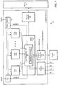
- Fig. 1 is a block diagram of one embodiment of an integrated circuit (IC) coupled to a memory.
- IC 2 is a processor having a number of processing nodes 11 (e.g., 11-1, 11-2, and so forth). It is noted that the methodology to be described herein may be applied to other arrangements, such as multi-processor computer systems implementing multiple processors (which may be single-core or multi-core processors) on separate, unique IC dies.
- processing nodes 11 may be identical to each other (i.e. homogonous multi-core), or one or more processing nodes 11 may be different from others (i.e. heterogeneous multi-core).
- Processing nodes 11 may each include one or more execution units, cache memories, schedulers, branch prediction circuits, and so forth. Furthermore, each of processing nodes 11 may be configured to assert requests for access to memory 6, which may function as the main memory for computer system 10. Such requests may include read requests and/or write requests, and may be initially received from a respective processor core 11 by north bridge 12. Requests for access to memory 6 may be routed through memory controller 18 in the embodiment shown.
- North bridge 12 may provide a wide variety of interface functions for each of processing nodes 11, including interfaces to memory and to various peripherals.
- north bridge 12 is also coupled to input/output (I/O) interface 13, graphics processing unit (GPU) 14, memory controller 18, phase-locked loop (PLL) 4, and voltage regulator 5. Additional functional units may also be included in some embodiments.
- North bridge 12 may serve as a communications hub for activity in computer system 10, routing and coordinating communications between processing nodes 11, memory 6 (via memory controller 18), display 3 (via GPU 14), and various peripheral devices (via I/O interface 13).
- I/O interface 13 may function as a south bridge device in computer system 10.
- peripheral buses may be coupled to I/O interface 13.
- the bus types include a peripheral component interconnect (PCI) bus, a PCI-Extended (PCI-X), a PCIE (PCI Express) bus, a gigabit Ethernet (GBE) bus, and a universal serial bus (USB).
- PCI peripheral component interconnect
- PCI-X PCI-Extended
- PCIE PCI Express
- GEE gigabit Ethernet
- USB universal serial bus
- Peripheral devices may be coupled to some or all of the peripheral buses.
- peripheral devices include (but are not limited to) keyboards, mice, printers, scanners, joysticks or other types of game controllers, media recording devices, external storage devices, network interface cards, and so forth.
- peripheral devices may assert memory access requests using direct memory access (DMA). These requests (which may include read and write requests) may be conveyed to north bridge 12 via I/O interface 13, and may be routed to memory controller 18.
- DMA direct memory access
- GPU 14 may perform video processing functions for computer system 10. Video processing functions performed by GPU 14 may include basic video rendering, as well as 3-D graphics and other types of complex graphics functions. The video information processed by GPU 14 may be output for display on display 3, which may be one of a number of different types of display units. Display 3 may be implemented as flat panel liquid crystal display (LCD), a light-emitting diode (LED) display, a plasma display, a cathode ray tube (CRT) display, or any other suitable type.
- LCD liquid crystal display
- LED light-emitting diode
- plasma display a cathode ray tube (CRT) display, or any other suitable type.
- CTR cathode ray tube
- GPU 14 may include a display buffer that may store data for display processing.
- the data for display processing may be read from memory 6, via memory controller 18 and north bridge 12.
- GPU 14 may be configured for direct memory access (DMA) of memory 6 for updating frames and filling the display buffer.
- DMA direct memory access
- north bridge 12 includes a power management unit 20 that is configured to manage the power consumption of each of processing nodes 11 based on their respective activity levels or workloads, as will be discussed in further detail below.
- power management unit 20 may set the operating points of the individual processing nodes 11 independent of one another.
- a first processor core 11 may operate at a first operating point
- a second processor core 11 may operate at a second operating point different than the first.
- GPU 14 may consume a significant amount of power (and generate a significant amount of heat)
- its respective operating point may also be controlled by power management unit 20 in the same manner as the operating points of processing nodes 11. Accordingly, the discussion below directed to setting a local TDP limit and controlling the operating point of a given one of processing nodes 11 may also apply to GPU 14.
- Power management unit 20 in the embodiment shown also includes a thermal control unit 21.
- the setting of operating points by power management unit 20 may be performed at least in part based on operations performed by thermal control unit 21.
- thermal control unit 21 may monitor temperature information received from each of the processing nodes 11 (and from graphics processing unit 14, which will be discussed below) in order to determine whether IC 2 is operating within a global TDP power limit (hereinafter referred to as a global power limit).
- thermal control unit 21 may also set and vary local TDP limits (hereinafter local power limits) for each of the processing cores 11. For example, in an embodiment having four processing nodes 11, if all four processing nodes 11 are active and processing a workload, their respective local power limits may be set to equal values.
- the local power limits for the active nodes may be increased with the local power limits for the idle nodes may be decreased correspondingly. In both of these, as well as other cases, the local power limits for processing nodes 11 may such that the global power limit is not exceeded.
- Thermal control unit 21 may also receive temperature information from each of processing nodes 11. The temperature information received may be used for determining whether the processing nodes 11 are operating within their respective local power limits. For example, thermal control unit 21 may compare a reported temperature of a given processor core 11 to a temperature threshold value that is based on its current local power limit. If the temperature is greater than or equal to the threshold temperature, power management unit 20 may respond by performing a limited throttling of the reporting processor core 11. The limited throttling may comprise a small reduction in the operating clock frequency for the reporting processor core 11, and may also include a limited voltage reduction. The operating point of that processor core 11 may be limited thereafter for a time at least until the temperature has fallen below the threshold. Additional time may be allowed for the temperature to allow for additional heat to be dissipated before removing the operating point limit.
- the limiting of the operating point may be performed on a per-node basis, applying only to the processor core 11 in which the temperature exceeded the threshold. In other embodiments, all processing nodes 11 may be limited to the same operating point of the processor core 11 for which the temperature threshold was exceeded.
- the operating point may be limited by limiting the frequency of the clock signal provided to the processing nodes 11. Further limiting of the operating point may be accomplished by limiting the operating voltage provided to the processing nodes 11.
- Thermal control unit 21 may also be configured to determine whether IC 2 as a whole is operating within a global power limit. In addition to receiving temperature information from processing nodes 11, thermal control unit 21 may receive the same from each of the other functional units, as well as from other functional units that may be present in other embodiments. If a temperature reading from any functional unit (or from any point on IC 2) exceeds a second temperature threshold, power management unit 20 may respond by globally throttling IC 2. Globally throttling may be defined by a significant reduction in clock frequency to each of processing nodes 11, and may be applied to the other functional units of IC2 as well. Furthermore, the operating voltage for each of processor core 11 may also be significantly reduced as well. The operating point for all processing nodes 11 subsequent to global throttling may be limited at least until all temperatures reported to thermal control unit 21 are below the second threshold, and may be limited for a specified time thereafter to allow IC 2 to further cool down.
- IC 2 includes a phase-locked loop (PLL) 4 coupled to receive a system clock signal.
- PLL 4 may distribute corresponding clock signals to each of processing nodes 11 and to GPU 14.
- the clock signals received by each of processing nodes 11 and GPU 14 are independent of one another.
- PLL 4 in this embodiment is configured to individually control and alter the frequency of each of the clock signals provided to respective ones of processing nodes 11, independently of one another.
- PLL 4 may also control and alter the frequency of the clock signal provided to GPU 14 independently of processing nodes 11.
- the frequency of the clock signal received by any given one of processing nodes 11 may be increased or decreased in accordance with a variable local power limit, temperature values reported therefrom, and performance demands imposed thereupon.
- the various frequencies at which clock signals may be output from PLL 4 may correspond to different operating points for each of processing nodes 11. Accordingly, a change of operating point for a particular one of processing nodes 11 may be put into effect by changing the frequency of its respectively received clock signal.
- power management unit 20 may change the state of digital signals SetF [M:0] provided to PLL 4.
- This set of digital signals may contain information for setting the clock frequency for each functional unit coupled to PLL 4. Responsive to the change in these signals, PLL 4 may change the clock frequency of the affected functional units.
- IC 2 also includes voltage regulator 5.
- voltage regulator 5 may be implemented separately from IC 2.
- Voltage regulator 5 may provide a operating voltage (or supply voltage) to each of processing nodes 11.
- voltage regulator 5 may provide an operating voltage that is variable according to a particular operating point (e.g., increased for greater performance, decreased for greater power savings).
- each of processing nodes 11 may share a voltage plane.
- each processor core 11 in such an embodiment operates at the same voltage as the other ones of processing nodes 11.
- voltage planes are not shared, and thus the supply voltage received by each processor core 11 may be set and adjusted independently of the respective supply voltages received by other ones of processing nodes 11.
- operating point adjustments that include adjustments of an operating voltage may be selectively applied to each processor core 11 independently of the others in embodiments having non-shared voltage planes.
- power management unit 20 may change the state of digital signals SetV[M:0] provided to voltage regulator 5. Responsive to the change in the signals SetV[M:0], voltage regulator 5 may adjust the operating voltage provided to the affected ones of processing nodes 11.
- GPU 14 may share a voltage plane with one or more of processing nodes 11 in some embodiments, while having its own voltage plane in other nodes, and may also have its supply voltage adjusted accordingly.
- operating points for each of processing nodes 11 may be set or limited based on reported temperatures, variable local power limits, and a fixed global power limit.
- operating points for each of processing nodes 11 may also be set in accordance with a respective activity level (e.g., processing workload).
- power management unit 20 may receive information indicating the activity level for each of processing nodes 11, and may set the operating point accordingly, within local and global power limits.
- Power management unit 20 may also set the operating point of a given processing node based on a particular type of workload. Generally speaking, a processor core 11 executing a compute-bounded workload may be set to a higher operating point, or to a lower operating point when executing a memory-bounded workload.
- a processor core 11 may be set to an intermediate operating point.
- Activity levels and types of workloads may be determined by power management unit 20 based on various metrics, such as committed instructions per second, memory access requests, cache hits/misses, pipeline stalls, branch mispredictions, instructions issued, instructions executed, and so forth.
- an operating point of a processor core 11 may be defined by at least a clock frequency, and may also be defined by an operating voltage. Generally speaking, transitioning to a "higher" operating point may be defined by increasing the clock frequency for the affected processor core 11. Transitioning to a higher operating point may also include increasing its operating voltage. Similarly, transitioning to a "lower” operating point may be defined by decreasing the clock frequency for the affected processor core 11. A decrease in the operating voltage provided to an affected processor core 11 may also be included in the definition of transitioning to a lower operating point.
- the operating points may correspond to performance states (hereinafter 'P-states') of the Advanced Configuration and Power Interface (ACPI) specification.
- Table 1 below lists P-states for one embodiment implemented using the ACPI standard.
- Table 1 P-state index Frequency Voltage P0 2 GHz 1.1 V P1 1.8 GHz 1.0 V P2 1.5 GHz 0.9 V P3 1 GHz 0.85 V P4 800 MHz 0.8 V
- P-states listed in Table 1 above may be applied when an ACPI-compliant processor is operating in a non-idle state known as C0.
- P-state P0 is the highest operating point, having a clock frequency of 2 GHz and an operating voltage of 1.1 volts.
- Power management unit 20 in one embodiment may cause a processor core 11 to operate at P-state P0 responsive to a high activity level when permitted by a current local power limit. Operation in P-state P0 may be utilized for processing workloads that are compute-bounded.
- a compute-bounded workload may be time sensitive and computationally intensive, requiring few (if any) memory accesses.
- compute-bounded workloads having a high activity level may be executed in P-state P0, which may enable faster completion.
- P-state P4 is the lowest operating point in this particular embodiment, having a clock frequency of 800 MHz and an operating voltage of 0.8V.
- Power management unit 20 may cause a processor core 11 to operate in P-state P4 responsive to a low activity level, even if higher P-states would fall within a current local power limit.
- P-state P4 may be used with memory-bounded workloads as well as with other tasks that are not time-sensitive (or frequency-sensitive).
- Memory-bounded workloads are those which include frequent accesses to system memory. Since memory accesses involve large latencies (in comparison with the execution times of instructions that do not access memory), reducing the clock frequency for memory-bounded workloads may have a minimal performance impact and with power savings that may improve the performance-per-watt metric of the system.
- operation of the corresponding processor core 11 may be set to any one of P-states P1, P2, P3, under direction of an OS, other software, firmware, and/or other hardware, depending on the specific embodiment and providing that operation in these P-states falls within current local power limits.
- the P-states listed in Table 1 are an exemplary set of operating points. Embodiments that use operating points having different clock frequencies and operating voltages are possible and contemplated. Further, as previously noted above, some embodiments may utilize a shared voltage plane for processing nodes 11, and thus their respective operating points may be defined on the basis of a clock frequency. In some embodiments, the operating voltage for each of the processing nodes may either remain fixed, while in other embodiments, the operating voltage may be adjusted for all processing nodes 11 at the same time. It is also noted that the operating points listed as P-states in Table 1 above may also be utilized with non-ACPI embodiments.
- a performance boost beyond the P0 state may be applied to a given processor core 11 when appropriate for the processing workload and permitted by a current local power limit. For example, consider a situation wherein a given one of processing nodes 11 is executing a compute-bounded workload while the remaining ones of processing nodes 11 are in an idle state. In such a case, the local power limit for the idle processing nodes may be reduced, while the local power limit for the active processor core 11 may be increased. The increase in the local power limit may thus enable overclocking for the active processor core 11.
- the frequency of the clock signal provided thereto may be increased to a value that is greater than that for the P0 state. This in turn may enable faster execution of the compute-bounded workload, and may be performed while allowing IC 2 to remain within the global power limit if the ambient temperature is low enough. Furthermore, if the ambient temperature is less than the value upon which the local power limit is based, overclocking the active processor core 11 may enable faster execution of the compute-bounded workload without the possibility of throttling. This type of deterministic performance may lead to greater performance-per-watt in low ambient temperature environments.
- TDP Global and Local Thermal Design Power
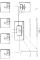
- Fig. 2 is a block diagram of one embodiment of a multi-core processor including a thermal control unit. More particularly, Fig. 2 illustrates the functional relationship between the various processing nodes 11, GPU 14, and thermal control unit 21. Fig. 2 also includes a graph illustrating the difference in system response based on local power limits (which may be variable and applied to functional units on an individual basis) and a global power limit (which may be fixed and applied to the IC as a whole).
- IC 2 includes four processing cores 11 (i.e., cores 11-1 to 11-4) and a GPU 14 each coupled to thermal control unit 21 of power management unit 20.
- processing cores 11 and GPU 14 may occupy a certain portion of the area of the die of IC 2.
- each of processing cores 11 and GPU 14 in the embodiment shown includes one or more sensors 19, each of which is configured to sense temperature within their respective units.
- multiple instances of sensor 19 may be placed in various locations throughout area of the IC die upon which each functional unit is implemented.
- each sensor 19 may be coupled to report a respectively sensed temperature to thermal control unit 21.
- each functional unit may be configured to report only the highest measured temperature for that functional unit.
- Sensors 19 may be implemented in a variety of ways.
- sensors 19 may be implemented as ring oscillator based temperature sensors.
- the ring oscillator in such temperatures may output a signal having a certain frequency, with the frequency increasing as temperature increases, and vice versa.
- Temperature sensors that output a voltage or current that is proportional to the measured temperature are also possible and contemplated.
- temperature values may be extrapolated from other information, such as an executed code stream or signals generated during operation.
- Thermal control unit 21 may compare the temperatures received from each of the functional units to a first temperature threshold and a second temperature threshold, as shown in the graph accompanying the block diagram in Fig. 2 .
- the first temperature threshold may be used in performing thermal control on a per node basis (PNTC), while the second temperature threshold may be used in performing thermal control on a global basis (HTC).
- the first temperature threshold is less than the second temperature threshold.
- Example values of the first and second temperature thresholds are 96° C and 100° C, respectively.
- the first temperature threshold may be based on a first ambient temperature (e.g., 28° C) and a maximum local power limit.
- the second temperature threshold may be based on a second ambient temperature (e.g., 35° C) and a global power limit.
- a temperature reading that is greater than the first temperature threshold may indicate that the reporting processing core 11 is exceeding it local power limit.
- a temperature reading that is greater than the second temperature threshold value may indicate that IC 2 as a whole is exceeding its global power limit.
- the reporting processor core 11 may be throttled. More particularly, the clock frequency of the reporting processor core 11 may be reduced to a specified level responsive to thermal control unit 21 determining that its temperature is greater than or equal to the first temperature threshold. In one ACPI-compliant embodiment, the clock frequency of at least the reporting processor core 11 may be reduced to 90% of the frequency of the P0 state. Furthermore, the clock frequency of the reporting processor core 11 may be limited to this operating point at least until its corresponding reported temperature falls below the first threshold, and may remain there for an additional amount of time to allow for additional cooling.
- processor cores 11 may also be limited in operating point to 90% of the frequency of the P0 state responsive to the one processor core 11 reporting a temperature that is greater than or equal to the first temperature threshold.
- processor cores 11 may also be limited in operating point to 90% of the frequency of the P0 state responsive to the one processor core 11 reporting a temperature that is greater than or equal to the first temperature threshold.
- the other active processor cores 11 are not limited in operating point when one particular processor core 11 reports a temperature greater than or equal to the first temperature threshold.
- thermal control unit 21 may respond by globally throttling all active processor cores 11.
- the clock frequency for active processor cores 11 may be throttled to 50% of the frequency of the P0 state. Active processor cores 11 that are already operating at a clock frequency of less than that of 50% of the P0 state may continue to operate as before. However, all processor cores 11 may be limited to an operating point in which the clock frequency is no more than 50% that of the P0 state.
- the operating voltage for each of processor cores 11 may also be limited. Referring back to Table 1, a clock frequency that is 50% of the frequency of the P0 state corresponds to the P3 state for that particular embodiment.
- the operating voltage in the P3 state in Table 1 is 0.85 volts (1.1. volts for the P0 state). Accordingly, in split-voltage plane embodiments (i.e. each processing core 11 has its own voltage plane), the operating voltage for any processor cores 11 operating at a voltage above that of the P3 state may be reduced to 0.85 volts responsive to thermal control unit 21 determining that a reported temperature reading is at or above the second temperature threshold.
- shared voltage plane embodiments i.e.
- the operating voltage for all processing cores 11 may be set to that of the P3 state. Similar operating voltage adjustments may be made in other embodiments, regardless of whether those embodiments are ACPI-compliant, and regardless of whether processor cores 11 utilize a shared voltage plane or separate voltage planes.
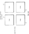
- Figs. 3A-3F are block diagrams illustrating thermal design power allocation for various situations in an embodiment of a processor that utilizes PNTC. More particularly, Figs. 3A-3F illustrate the local power limit distribution for the various processor cores 11 when each of the cores is in one of a number of various states of activity or idleness. It is noted that idleness for a given one of processor cores 11 may include a clock-gated state (i.e. in which power remains applied by the clock signal to the core is inhibited) and a power-gated state (i.e. when the clock signal is not provided to the core and power is removed therefrom).
- a clock-gated state i.e. in which power remains applied by the clock signal to the core is inhibited
- a power-gated state i.e. when the clock signal is not provided to the core and power is removed therefrom.
- Figs. 3A-3F do not include local power limits that are assigned to GPU 14.
- Figs. 3A-3F are presented for illustrative purposes, and that in various embodiments, a local power limit for a GPU such as GPU 14 may be assigned and varied using the same principles as discussed herein.
- Fig. 3A all processor cores 11 are active and executing a processing workload.
- the global power limit is 40 watts. Since each of the four-processor cores 11 in this embodiment is active, thermal control unit 21 may assign a local power limit of 10 watts to each, thereby evenly distributing local power limits. If the embodiment shown is an ACPI-compliant embodiment conforming the figures presented in Table 1 above, the maximum clock frequency for any of processor cores 11 may be 2.0 GHz, although intermittent boosts of up to 3.2 GHz may be permitted.
- each of processor cores 11 may operate at 2.0 GHz with the intermittent boosts of 3.2 GHz in a deterministic, repeatable manner for environments in which the ambient temperature is less than 28° C. If the ambient temperature is greater than 28° C, the configuration shown in Fig. 3A may still be permitted, although some throttling (e.g., as described in reference to Fig. 2 ) may occur.
- Fig. 3B two of processing cores 11 are idle, while the other two are active.
- the idle processor cores in this example may be clock-gated (i.e. the clock signal to these cores is inhibited) but not power-gated.
- the local power limit for the active cores may be set at 15 watts each.
- the 15 watt local power limit for the two active processor cores 11 may enable a performance boost via overclocking for these cores.
- each of the two active processor cores 11 may be operated at a clock frequency of up to 3.2 GHz.
- operation of the two active cores may be accomplished without the need for throttling due to exceeding local or global power limits.
- operation of one or both of the active processor cores 11 at 3.2 GHz may result in some throttling.
- the actual clock frequency of operation may also depend on its processing workload. For example, if the processing workload for an active processor core in the example of Fig. 3B is compute-bounded, the clock frequency may be increased to 3.2 GHz. However, if the processing workload for an active processor core 11 in the example of Fig. 3B is memory-bounded (and thus not sensitive to the core clock frequency), the core may be operated as a significantly lower clock frequency, since increasing it in this situation would not result in any appreciable performance gain.
- the 5 watt local power limit for each of these may provide a margin of power should an event occur that causes one or both of these cores to enter an active state.
- the two idle processor cores 11 may act as a thermal sink with respect to the two active cores.
- the assignment of local power limits to the various processor cores 11 may depend on the geometry of the layout on the IC die upon which the cores are implemented. For example, if an active core is located physically adjacent to an idle core, its local power limit may be greater than if it is located physically adjacent to another active core.
- processor cores 11 are in an idle (clock-gated) state, while one of processor cores 11 is active.
- the active processor core 11 may be assigned a local power limit of 19 watts, and may be overclocked to a frequency of up to 3.6 GHz.
- the active processor core 11 may operate within its assigned local power limit for ambient temperatures below a specified value (e.g., the 28° C value mentioned above). Above the specified value, operating at a clock frequency of 3.6 GHz may result in some throttling of the active processor core 11.
- Fig. 3D illustrates a situation that is similar to that of Fig. 3B , wherein two processor cores 11 are idle, while the other two are active.
- a local power limit of 13 watts each may be assigned.
- the active processor cores 11 may operate at a clock frequency of up to 3.4 GHz in this example, compared to a maximum clock frequency of 3.2 GHz for the example of Fig. 3B .
- the difference between the local power limit values in this example in comparison to the example of Fig. 3B may be a result of one or more of a number of different factors.
- One such factor is the layout geometry of the IC die upon which the processor cores 11 are implemented.
- the two active processor cores 11 may each be physically adjacent to an idle processor core 11, but not to each other.
- the two active processor cores 11 in the example of Fig. 3D may be physically adjacent to one another. Accordingly, in the example of Fig. 3B , the heat generated by the active processor cores 11 may be more easily dissipated than in the example of Fig. 3D .
- thermal control unit 21 may be quicker to perform PNTC throttling (as discussed above in reference to Fig. 2 ) for the active cores 11 due to the lower local power limit relative to that of Fig. 3B . This may make it less likely that global (HTC) throttling (as also discussed above in reference to Fig. 2 ) will be necessary.
- two processor cores 11 are power-gated (i.e. powered down), another processor core 11 is idle (clock-gated), while one processor core 11 is active.
- the active processor core 11 may be assigned a local power limit of 26 watts, with a maximum clock frequency of 3.9 GHz. It is noted that in this situation, the maximum power consumption adds up to 35.6 watts, which is less than the 40 watt global power limit. This difference may provide a guard band in the case where one of the idle or power-gated processor cores enters an active state due to a wake-up event.
- Fig. 3F two processor cores 11 are power-gated, while the remaining two are active.
- the active processor cores 11 are each assigned a local power limit of 17 watts, with a maximum clock frequency of 3.8 GHz.
- the maximum power consumption in this case adds up to 34.6 watts, which is again less than 40 watt global power limit.
- the difference between the total amount of assigned local power limits and the global power limit may allow a guard band in the case where one of the idle or power-gated processor cores enters an active state due to a wake-up event.
- Fig. 4 is a graph illustrating the maximum core power that may be utilized under two different scenarios for one embodiment of a multi-core processor. More particularly, Fig. 4 illustrates the difference in maximum core power utilization that is achievable using PNTC, as opposed to an embodiment that utilizes only global HTC. On the left hand side of the graph, the maximum core power for an embodiment configured for PNTC is illustrated. On the right hand side of the graph, the maximum core power for an embodiment configured for HTC only is illustrated. Since the local power limits applied to the processor cores utilizing PNTC is based on a lower ambient temperature than for the global power limit, additional power may be consumed on a per-core basis in the PNTC embodiment. This may in turn allow for performance boosting of the processor cores to utilize the extra power available.
- this performance boosting may be accomplished by increasing the core clock frequency beyond its maximum frequency of a highest specified operating point (e.g., to a value greater than the maximum frequency specified in the ACPI-compliant embodiment exemplified in Table 1). Increasing the clock frequency in such a manner is known as overclocking. If a workload demand on given processor core justifies such a frequency increase commensurate with overclocking, the processor core may be enabled to execute that workload faster than might otherwise be achievable in an embodiment that relies solely on globally-applied HTC.
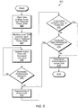
- Figs. 5 and 6 illustrate embodiments of various methods that may be utilized in a multi-core processor configured for PNTC.
- Fig. 5 is a flow diagram of one embodiment of a method for boosting performance of a processor core based on a local power limit in a PNTC processor embodiment.
- Fig. 6 is a flow diagram of one embodiment of a method for using both PNTC and global HTC in a multi-core processor.
- Method 500 of Fig. 5 begins with the placing of one or more inactive processor cores into a reduced power state (block 502).
- the reduce power state may be a clock-gated state or a power-gated state.
- the clock signal may be inhibited from being provided to the cores placed in the reduced power state, although the operating voltage may continue to be provided.
- the power-gated state neither the clock signal nor operating voltage is provided to the cores placed in a reduced power state.
- their respective local power limits may also be reduced (block 504).
- One or more processor cores that remain active may each continue to operate with an increased local power limit (block 506).
- the local power limits for one and optionally more remaining active processor cores are increased responsive to the reduction of the local power limits of those cores placed in a reduced power state. If the performance demand for the active core does not increase or is otherwise relatively low (block 508, no), then the cores may continue to operate at their current operating point. However, if the performance demand for a remaining active core increases or is otherwise relatively high (block 508, yes), the increase in the local power limit allows for increasing the operating point to maximize performance. In the embodiment shown, this is achieved by overclocking each active core having a high or increased performance demand (block 510). Overclocking is performed for compute-bounded processor workloads.
- Overclocking may continue for an active processor core under two conditions.
- the first of these conditions is that the highest temperature reported for that core remains less than a first temperature threshold that is used for PNTC (e.g., see graph in Fig. 2 above). If the temperature remains below the first threshold (block 512,no), and the performance demand of the processor workload remains high enough to justify the higher operating point (block 514, yes), then overclocking may continue (block 510). If a reported temperature from an overclocking processor core meets or exceeds the first threshold value (block 512, yes) or the workload demand decreases to a point where overclocking provides no performance advantage (block 514), then overclocking may be discontinued (block 516).
- throttling of the reporting core may be performed. In one ACPI-compliant embodiment, this throttling may limit the operating point of the reporting core to one having a clock frequency that is 90% that of the P0 state.
- FIG. 5 illustrates a single iteration of the method to which it pertains. However, it is noted that this method may be repeated as many times as necessary during the operation of the processor in which PNTC is utilized.
- Fig. 6 is a flow diagram illustrating the use of both PNTC and HTC on the same processor.
- method 600 begins with the monitoring of reported temperatures for each of a number of processor cores (block 602).
- the monitoring of reported temperatures may include comparing these values to first and second threshold values, such as those shown in the graph of Fig. 2 . If no reported temperature on the IC die is greater than or equal to either of the first and second threshold (block 604, no), then no throttling or other power reduction action is performed (block 616) responsive to the temperature readings.
- decreases in respective operating points for the various processor cores may occur responsive to reduced workload demands. Such operating point decreases may include clock-gating and power-gating of the processor cores for which the performance demand is reduced.
- a temperature reported from a given core meets or exceeds the first temperature threshold (block 604, yes), but no core is reporting a temperature meeting or exceeding the second temperature threshold (block 606, no)
- the given core may be throttled and its operating point (e.g., P-state) limited (block 608).
- P-state e.g., P-state
- PNTC per node basis
- HTC global basis
- the operating point is limited only for the reporting core. In other embodiments, all cores may be limited in operating point in the same manner as the reporting core. Further still, some embodiments may allow for a partial limiting of the operating point. For example, in an embodiment wherein a voltage plane is shared among all cores, the operating voltage for all cores may be limited to a specified value (e.g., 90% of the operating voltage for the P0 state of Fig. 1 ), while the clock frequencies for the non-reporting cores are not limited.
- a specified value e.g. 90% of the operating voltage for the P0 state of Fig. 1
- the operating point for all cores may be limited to 50% of the clock frequency of the P0 state, i.e. an operating point that corresponds to the P3 state.
- the operating voltage may be similarly limited to that specified by the P3 state.
- Those processor cores operating at a clock frequency that is greater than that specified by the P3 state may be throttled responsive to the reported temperature being greater than or equal to the second temperature threshold.
- processor cores operating at a clock frequency and operating voltage equal to or less than that of the P3 state may continue operating at their respective operating points, although these cores may not respond to an increased workload demand by increasing to an operating point higher than the P3 state while the operating points for all cores remain limited.
- the temperatures may continue to be monitored. If the reported temperatures are not below the first and second temperature threshold values (block 612, no), then operating point limiting may continue (block 614). If all temperatures are within limits (block 612, yes), then the processor cores may be operated based on respective performance demands and respective local power limits, without limiting the operating point to a state that is less than the maximum specified.
- operating point limiting may continue for a time thereafter to allow for additional cooling of the IC.
- An embodiment utilizing a third temperature threshold is thus contemplated.
- the third temperature threshold may be less than either of the first or second temperature thresholds.
- one or more of the processing cores may continue to be limited until one or more reported temperatures falls below a the third temperature threshold. For example, if a single core is throttled and/or limited in operating point using PNTC responsive to reporting a temperature exceeding the first temperature threshold, that core may continue to be operating point limited until its maximum reported temperature falls below the third threshold.
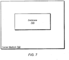
- a computer accessible storage medium 400 may include any non-transitory storage media accessible by a computer during use to provide instructions and/or data to the computer.
- a computer accessible storage medium 400 may include storage media such as magnetic or optical media, e.g., disk (fixed or removable), tape, CD-ROM, or DVD-ROM, CD-R, CD-RW, DVD-R, DVD-RW, or Blu-Ray.
- Storage media may further include volatile or non-volatile memory media such as RAM (e.g.
- SDRAM synchronous dynamic RAM
- DDR double data rate SDRAM
- LPDDR2, etc. low-power DDR SDRAM
- RDRAM Rambus DRAM
- SRAM static RAM
- ROM Flash memory
- Flash memory non-volatile memory (e.g. Flash memory) accessible via a peripheral interface such as the Universal Serial Bus (USB) interface
- Storage media may include microelectromechanical systems (MEMS), as well as storage media accessible via a communication medium such as a network and/or a wireless link.
- MEMS microelectromechanical systems
- the data 705 representative of the system 10 carried on the computer accessible storage medium 700 may be a database or other data structure which can be read by a program and used, directly or indirectly, to fabricate the hardware comprising the system 10.
- the database 705 may be a behavioral-level description or register-transfer level (RTL) description of the hardware functionality in a high level design language (HDL) such as Verilog or VHDL.
- the description may be read by a synthesis tool which may synthesize the description to produce a netlist comprising a list of gates from a synthesis library.
- the netlist comprises a set of gates which also represent the functionality of the hardware comprising the system 10.
- the netlist may then be placed and routed to produce a data set describing geometric shapes to be applied to masks.
- the masks may then be used in various semiconductor fabrication steps to produce a semiconductor circuit or circuits corresponding to the system 10.
- the database 705 on the computer accessible storage medium 700 may be the netlist (with or without the synthesis library) or the data set, as desired, or Graphic Data System (GDS) II data.
- GDS Graphic Data System
- the computer accessible storage medium 700 carries a representation of the system 10
- other embodiments may carry a representation of any portion of the system 10, as desired, including IC 2, any set of agents (e.g., processing cores 11, I/O interface 13, power management unit 20, etc.) or portions of agents (e.g., thermal control unit 21, etc.).
- agents e.g., processing cores 11, I/O interface 13, power management unit 20, etc.
- portions of agents e.g., thermal control unit 21, etc.
Landscapes
- Engineering & Computer Science (AREA)
- Theoretical Computer Science (AREA)
- Physics & Mathematics (AREA)
- General Engineering & Computer Science (AREA)
- General Physics & Mathematics (AREA)
- Human Computer Interaction (AREA)
- Power Sources (AREA)
- Microcomputers (AREA)
Claims (16)
- System, umfassend:eine Vielzahl von Verarbeitungsknoten (11); undeine Leistungsverwaltungseinheit (20), die eine Schaltung umfasst, wobei die Schaltung zu Folgendem konfiguriert ist:ein Einstellen einer ersten Frequenzgrenze für einen der Vielzahl von Verarbeitungsknoten, unabhängig von anderen der Vielzahl von Verarbeitungsknoten, als Reaktion auf ein Empfangen einer Anzeige, dass eine erste erfasste Temperatur größer als ein erster Temperaturschwellenwert ist, wobei die erste erfasste Temperatur dem einen der Vielzahl von Verarbeitungsknoten zugeordnet ist;das Einstellen einer zweiten Frequenzgrenze für jeden der Vielzahl von Verarbeitungsknoten, als Reaktion auf das Empfangen einer Anzeige, dass eine zweite Temperatur größer als ein zweiter Temperaturschwellenwert ist, wobei der zweite Temperaturschwellenwert größer als der erste Temperaturschwellenwert ist;das Einstellen einer Frequenz eines bestimmten Verarbeitungsknotens auf eine erste Frequenz;ein Erhöhen eines Grenzwerts der lokalen Wärmeverlustleistung (thermal design power - TDP) des bestimmten Verarbeitungsknotens als Reaktion darauf, dass ein oder mehrere Knoten, ungleich vom bestimmten Verarbeitungsknoten, der Vielzahl von Verarbeitungsknoten in einen Zustand verringerter Leistungsaufnahme versetzt wird/werden;ein Verursachen eines Übertaktens des bestimmten Verarbeitungsknotens, wodurch eine Frequenz des bestimmten Verarbeitungsknotens auf eine zweite Frequenz erhöht wird, die höher als die erste Frequenz ist, als Reaktion auf ein Bestimmen, dass der bestimmte Verarbeitungsknoten eine rechengebundene Arbeitslast verarbeitet und der lokale TDP-Grenzwert eine Erhöhung bei einer Taktfrequenz des bestimmten Verarbeitungsknotens zulässt; unddas Einstellen des bestimmten Verarbeitungsknotens auf einen niedrigeren Betriebspunkt durch das Senken der Frequenz des bestimmten Verarbeitungsknotens auf eine dritte Frequenz, die niedriger als die erste Frequenz ist, als Reaktion auf das Bestimmen, dass der bestimmte Verarbeitungsknoten eine speichergebundene Arbeitslast verarbeitet.
- Verfahren, das die folgenden Schritte umfasst, die von einer Leistungsverwaltungseinheit (20) durchgeführt werden:das Einstellen einer ersten Frequenzgrenze für einen einer Vielzahl von Verarbeitungsknoten (11), unabhängig von der Frequenz von anderen der Vielzahl von Verarbeitungsknoten, als Reaktion auf ein Empfangen einer Anzeige, dass eine erste erfasste Temperatur größer als ein erster Temperaturschwellenwert ist, wobei die erste erfasste Temperatur dem einen der Vielzahl von Verarbeitungsknoten zugeordnet ist;das Einstellen einer zweiten Frequenzgrenze für jeden der Vielzahl von Verarbeitungsknoten, als Reaktion auf das Empfangen einer Anzeige, dass eine zweite erfasste Temperatur größer als ein zweiter Temperaturschwellenwert ist, wobei der zweite Temperaturschwellenwert größer als der erste Temperaturschwellenwert ist;das Einstellen einer Frequenz eines bestimmten Verarbeitungsknotens auf eine erste Frequenz;das Erhöhen eines lokalen TDP-Grenzwerts des bestimmten Verarbeitungsknotens als Reaktion darauf, dass ein oder mehrere Knoten, ungleich vom bestimmten Verarbeitungsknoten, der Vielzahl von Verarbeitungsknoten in einen Zustand verringerter Leistungsaufnahme versetzt wird/werden;das Verursachen des Übertaktens des bestimmten Verarbeitungsknotens, wodurch eine Frequenz des bestimmten Verarbeitungsknotens auf eine zweite Frequenz erhöht wird, die höher als die erste Frequenz ist, als Reaktion auf ein Bestimmen, dass der bestimmte Verarbeitungsknoten eine rechengebundene Arbeitslast verarbeitet und der lokale TDP-Grenzwert eine Erhöhung bei einer Taktfrequenz des bestimmten Verarbeitungsknotens zulässt; unddas Einstellen des bestimmten Verarbeitungsknotens auf einen niedrigeren Betriebspunkt durch das Senken einer Frequenz des bestimmten Verarbeitungsknotens auf eine dritte Frequenz, die niedriger als die erste Frequenz ist, als Reaktion auf das Bestimmen, dass der bestimmte Verarbeitungsknoten eine speichergebundene Arbeitslast verarbeitet.
- System nach Anspruch 1, wobei jeder der Vielzahl von Verarbeitungsknoten dazu konfiguriert ist, an einem einer Vielzahl von Betriebspunkten zu arbeiten, wobei jeder der Vielzahl von Betriebspunkten eine Taktfrequenz und eine Versorgungsspannung umfasst, und wobei die Leistungsverwaltungseinheit ferner dazu konfiguriert ist, einen ersten Betriebspunktgrenzwert für den einen der Vielzahl von Verarbeitungsknoten als Reaktion auf das Empfangen einer Anzeige einzustellen, dass eine erste erfasste Temperatur größer als oder gleich dem ersten Temperaturschwellenwert ist, und ferner dazu konfiguriert, einen zweiten Betriebspunktgrenzwert für jeden der Vielzahl von Verarbeitungsknoten als Reaktion auf das Empfangen einer Anzeige einzustellen, dass eine zweite Temperatur größer als oder gleich dem zweiten Temperaturschwellenwert ist.
- Verfahren nach Anspruch 2, ferner umfassend ein Betreiben von jedem der Vielzahl von Verarbeitungsknoten an einem einer Vielzahl von Betriebspunkten, wobei jeder der Vielzahl von Betriebspunkten eine Taktfrequenz und eine Versorgungsspannung umfasst und wobei das Verfahren ferner Folgendes beinhaltet:das Einstellen eines ersten Betriebspunktgrenzwerts für den einen der Vielzahl von Verarbeitungsknoten als Reaktion auf das Empfangen der Anzeige, dass die erste erfasste Temperatur größer als oder gleich dem ersten Temperaturschwellenwert ist; unddas Einstellen eines zweiten Betriebspunktgrenzwerts für jeden der Vielzahl von Verarbeitungsknoten als Reaktion auf das Empfangen der Anzeige, dass die zweite erfasste Temperatur größer als oder gleich dem zweiten Temperaturschwellenwert ist.
- System nach Anspruch 3 oder Verfahren nach Anspruch 4, wobei der erste Betriebspunktgrenzwert einen Betriebspunkt umfasst, der eine erste Taktfrequenz aufweist, die kleiner als eine maximale Betriebsfrequenz ist, und ferner eine erste Versorgungsspannung umfasst, die geringer als eine Maximalversorgungsspannung ist.
- System oder Verfahren nach Anspruch 5, wobei der zweite Betriebspunktgrenzwert einen Betriebspunkt umfasst, der eine zweite Taktfrequenz, die kleiner als die erste Taktfrequenz ist, und eine zweite Versorgungsspannung aufweist, die geringer als die erste Versorgungsspannung ist.
- System nach Anspruch 1 oder Verfahren nach Anspruch 2, wobei der erste Temperaturschwellenwert für jeden der Vielzahl von Verarbeitungsknoten auf einem entsprechenden lokalen TDP-Grenzwert basiert, und wobei der zweite Temperaturschwellenwert auf einem globalen TDP-Grenzwert basiert, wobei die Leistungsverwaltungseinheit dazu konfiguriert ist, den lokalen TDP-Grenzwert für jeden der Vielzahl von Verarbeitungsknoten während des Betriebs zu variieren, und wobei der globale TDP-Grenzwert während des Betriebs feststehend ist.
- System nach Anspruch 7, wobei die Leistungsverwaltungseinheit dazu konfiguriert ist, ein Übertakten von mindestens einem der Vielzahl von Verarbeitungsknoten zu verursachen, wenn sein entsprechender lokaler TDP-Grenzwert größer als der lokale TDP-Grenzwert der anderen der Vielzahl von Verarbeitungsknoten ist.
- Verfahren nach Anspruch 7, ferner umfassend das Übertakten von mindestens einem der Vielzahl von Verarbeitungsknoten, wenn sein entsprechender lokaler TDP-Grenzwert größer als ein TDP-Grenzwert für die anderen der Vielzahl von Verarbeitungsknoten ist.
- System nach Anspruch 7, wobei die Leistungsverwaltungseinheit dazu konfiguriert ist, den lokalen TDP-Grenzwert für einen bestimmten der Vielzahl von Verarbeitungsknoten auf Grundlage entsprechender Betriebspunkte von einem oder mehreren zusätzlichen der Vielzahl von Verarbeitungsknoten einzustellen.
- Verfahren nach Anspruch 7, ferner umfassend das Einstellen des lokalen TDP-Grenzwerts für einen bestimmten der Vielzahl von Verarbeitungsknoten auf Grundlage entsprechender Betriebspunkte von einem oder mehreren zusätzlichen der Vielzahl von Verarbeitungsknoten.
- Verfahren nach Anspruch 11, ferner umfassend das Erhöhen des lokalen TDP-Grenzwerts für den bestimmten der Vielzahl von Verarbeitungsknoten als Reaktion darauf, dass eine zusätzlicher oder mehrere zusätzliche der Vielzahl von Verarbeitungsknoten in einem Ruhezustand übergehen.
- System oder Verfahren nach Anspruch 7, wobei der globale TDP-Grenzwert auf einem festgelegten Umgebungstemperaturwert basiert.
- System nach Anspruch 1 oder Verfahren nach Anspruch 2, wobei einer oder mehrere der Verarbeitungsknoten ein Prozessorkern ist, und wobei mindestens einer der Verarbeitungsknoten eine Grafikverarbeitungseinheit ist.
- System nach Anspruch 1, wobei die Leistungsverwaltungseinheit dazu konfiguriert ist, entsprechende Betriebspunkte für jeden der Vielzahl von Verarbeitungsknoten unabhängig voneinander einzustellen.
- Verfahren nach Anspruch 2, ferner umfassend das Einstellen entsprechender Betriebspunkte für jeden der Vielzahl von Verarbeitungsknoten unabhängig voneinander.
Applications Claiming Priority (2)
| Application Number | Priority Date | Filing Date | Title |
|---|---|---|---|
| US12/915,361 US8793512B2 (en) | 2010-10-29 | 2010-10-29 | Method and apparatus for thermal control of processing nodes |
| PCT/US2011/057640 WO2012058202A1 (en) | 2010-10-29 | 2011-10-25 | Method and apparatus for thermal control of processing nodes |
Publications (2)
| Publication Number | Publication Date |
|---|---|
| EP2635948A1 EP2635948A1 (de) | 2013-09-11 |
| EP2635948B1 true EP2635948B1 (de) | 2021-07-07 |
Family
ID=44983699
Family Applications (1)
| Application Number | Title | Priority Date | Filing Date |
|---|---|---|---|
| EP11782700.6A Active EP2635948B1 (de) | 2010-10-29 | 2011-10-25 | Verfahren und vorrichtung zur wärmesteuerung von verarbeitungsknoten |
Country Status (6)
| Country | Link |
|---|---|
| US (1) | US8793512B2 (de) |
| EP (1) | EP2635948B1 (de) |
| JP (1) | JP5770300B2 (de) |
| KR (1) | KR101845504B1 (de) |
| CN (1) | CN103189814B (de) |
| WO (1) | WO2012058202A1 (de) |
Families Citing this family (88)
| Publication number | Priority date | Publication date | Assignee | Title |
|---|---|---|---|---|
| US8984305B2 (en) * | 2010-12-21 | 2015-03-17 | Intel Corporation | Method and apparatus to configure thermal design power in a microprocessor |
| US8484496B2 (en) * | 2011-04-22 | 2013-07-09 | Qualcomm Incorporated | Method and system for thermal management of battery charging concurrencies in a portable computing device |
| US8185758B2 (en) * | 2011-06-30 | 2012-05-22 | Intel Corporation | Method and system for determining an energy-efficient operating point of a platform |
| US8930724B2 (en) * | 2011-08-17 | 2015-01-06 | Broadcom Corporation | Semiconductor device predictive dynamic thermal management |
| US8769316B2 (en) | 2011-09-06 | 2014-07-01 | Intel Corporation | Dynamically allocating a power budget over multiple domains of a processor |
| US9074947B2 (en) | 2011-09-28 | 2015-07-07 | Intel Corporation | Estimating temperature of a processor core in a low power state without thermal sensor information |
| US8954770B2 (en) * | 2011-09-28 | 2015-02-10 | Intel Corporation | Controlling temperature of multiple domains of a multi-domain processor using a cross domain margin |
| US8832478B2 (en) | 2011-10-27 | 2014-09-09 | Intel Corporation | Enabling a non-core domain to control memory bandwidth in a processor |
| US9026815B2 (en) | 2011-10-27 | 2015-05-05 | Intel Corporation | Controlling operating frequency of a core domain via a non-core domain of a multi-domain processor |
| US8943340B2 (en) | 2011-10-31 | 2015-01-27 | Intel Corporation | Controlling a turbo mode frequency of a processor |
| US9158693B2 (en) | 2011-10-31 | 2015-10-13 | Intel Corporation | Dynamically controlling cache size to maximize energy efficiency |
| US9304570B2 (en) * | 2011-12-15 | 2016-04-05 | Intel Corporation | Method, apparatus, and system for energy efficiency and energy conservation including power and performance workload-based balancing between multiple processing elements |
| US20120095607A1 (en) * | 2011-12-22 | 2012-04-19 | Wells Ryan D | Method, Apparatus, and System for Energy Efficiency and Energy Conservation Through Dynamic Management of Memory and Input/Output Subsystems |
| BR112014013999A2 (pt) * | 2011-12-29 | 2017-06-13 | Intel Corp | estrangulamento térmico adaptável com capacidade de configuração do usuário |
| CN104246651B (zh) * | 2012-03-29 | 2018-04-27 | 英特尔公司 | 平台中的动态功率限值共享 |
| US9360909B2 (en) * | 2012-04-19 | 2016-06-07 | Intel Corporation | System, method and apparatus for energy efficiency and energy conservation by configuring power management parameters during run time |
| US9383789B2 (en) | 2012-06-21 | 2016-07-05 | Apple Inc. | Thermal control apparatus and methodology |
| US9218045B2 (en) * | 2012-06-30 | 2015-12-22 | Intel Corporation | Operating processor element based on maximum sustainable dynamic capacitance associated with the processor |
| KR101975409B1 (ko) * | 2012-07-26 | 2019-05-08 | 삼성전자주식회사 | 시스템 온 칩 및 그것의 온도 제어 방법 |
| US9285818B2 (en) * | 2012-07-26 | 2016-03-15 | Qualcomm Incorporated | Autonomous thermal controller for power management IC |
| US9075611B2 (en) * | 2012-09-12 | 2015-07-07 | Htc Corporation | Electronic device with power management mechanism and power management method thereof |
| US9164931B2 (en) | 2012-09-29 | 2015-10-20 | Intel Corporation | Clamping of dynamic capacitance for graphics |
| CN103810141A (zh) * | 2012-11-09 | 2014-05-21 | 辉达公司 | 处理器和包括其的电路板 |
| US9946319B2 (en) * | 2012-11-20 | 2018-04-17 | Advanced Micro Devices, Inc. | Setting power-state limits based on performance coupling and thermal coupling between entities in a computing device |
| KR102005765B1 (ko) | 2012-12-17 | 2019-07-31 | 삼성전자주식회사 | 시스템-온 칩과, 이의 동작 방법 |
| DE102012112672A1 (de) * | 2012-12-19 | 2014-06-26 | Endress + Hauser Gmbh + Co. Kg | Verfahren zur Stabilisierung der Taktfrequenz eines Microcontrollers |
| US8975954B2 (en) * | 2013-01-08 | 2015-03-10 | Qualcomm Incorporated | Method for performing adaptive voltage scaling (AVS) and integrated circuit configured to perform AVS |
| US9494996B2 (en) | 2013-03-15 | 2016-11-15 | Intel Corporation | Processor having frequency of operation information for guaranteed operation under high temperature events |
| US9411395B2 (en) * | 2013-04-18 | 2016-08-09 | Intel Corporation | Method and apparatus to control current transients in a processor |
| US9360906B2 (en) | 2013-05-01 | 2016-06-07 | Advanced Micro Devices, Inc. | Power management for multiple compute units |
| US9195291B2 (en) | 2013-06-21 | 2015-11-24 | Apple Inc. | Digital power estimator to control processor power consumption |
| US9304573B2 (en) * | 2013-06-21 | 2016-04-05 | Apple Inc. | Dynamic voltage and frequency management based on active processors |
| US9471088B2 (en) * | 2013-06-25 | 2016-10-18 | Intel Corporation | Restricting clock signal delivery in a processor |
| US9377836B2 (en) | 2013-07-26 | 2016-06-28 | Intel Corporation | Restricting clock signal delivery based on activity in a processor |
| US9250910B2 (en) | 2013-09-27 | 2016-02-02 | Intel Corporation | Current change mitigation policy for limiting voltage droop in graphics logic |
| US9389675B2 (en) * | 2013-12-19 | 2016-07-12 | International Business Machines Corporation | Power management for in-memory computer systems |
| US9514715B2 (en) | 2013-12-23 | 2016-12-06 | Intel Corporation | Graphics voltage reduction for load line optimization |
| KR101538458B1 (ko) | 2014-01-03 | 2015-07-23 | 연세대학교 산학협력단 | 3차원 매니코어 프로세서를 위한 전압섬 형성 방법 |
| US9182768B2 (en) * | 2014-01-08 | 2015-11-10 | Nvidia Corporation | Voltage optimization circuit and managing voltage margins of an integrated circuit |
| US10067555B2 (en) * | 2014-02-20 | 2018-09-04 | Advanced Micro Devices, Inc. | Control of performance levels of different types of processors via a user interface |
| US9606605B2 (en) | 2014-03-07 | 2017-03-28 | Apple Inc. | Dynamic voltage margin recovery |
| EP3126928A4 (de) * | 2014-04-04 | 2017-11-08 | Empire Technology Development LLC | Anweisungsoptimierung mit spannungsbasierter funktionaler leistungsvariation |
| US9977439B2 (en) | 2014-04-08 | 2018-05-22 | Qualcomm Incorporated | Energy efficiency aware thermal management in a multi-processor system on a chip |
| US9671767B2 (en) * | 2014-05-14 | 2017-06-06 | Advanced Micro Devices, Inc. | Hybrid system and method for determining performance levels based on thermal conditions within a processor |
| US9652019B2 (en) | 2014-06-02 | 2017-05-16 | Advanced Micro Devices, Inc. | System and method for adjusting processor performance based on platform and ambient thermal conditions |
| US9400308B2 (en) * | 2014-07-03 | 2016-07-26 | Qualcomm Incorporated | Multi-domain heterogeneous process-voltage-temperature tracking for integrated circuit power reduction |
| US9791904B2 (en) * | 2014-08-15 | 2017-10-17 | Intel Corporation | Balanced control of processor temperature |
| CN105829991B (zh) * | 2014-09-17 | 2020-02-04 | 联发科技股份有限公司 | 操作计算系统的方法及其计算系统 |
| US9811142B2 (en) | 2014-09-29 | 2017-11-07 | Apple Inc. | Low energy processor for controlling operating states of a computer system |
| US9903764B2 (en) | 2014-09-30 | 2018-02-27 | Samsung Electronics Co., Ltd. | Integrated circuit for estimating power of at least one node using temperature and a system including the same |
| US10209758B2 (en) | 2014-12-12 | 2019-02-19 | Via Alliance Semiconductor Co., Ltd. | Graphics processing system and power gating method thereof |
| US10877530B2 (en) * | 2014-12-23 | 2020-12-29 | Intel Corporation | Apparatus and method to provide a thermal parameter report for a multi-chip package |
| US10216526B2 (en) * | 2015-01-14 | 2019-02-26 | Mediatek Inc. | Controlling method for optimizing a processor and controlling system |
| US10698459B2 (en) * | 2015-02-17 | 2020-06-30 | Apple Inc. | Electronic devices and method of controlling an electronic device |
| US9860189B2 (en) * | 2015-04-30 | 2018-01-02 | Dell Products Lp | Systems and methods to enable network communications for management controllers |
| US10429909B2 (en) * | 2015-06-01 | 2019-10-01 | Hewlett Packard Enterprise Development Lp | Managing power in a high performance computing system for resiliency and cooling |
| CN105045702B (zh) * | 2015-07-22 | 2018-03-20 | Tcl移动通信科技(宁波)有限公司 | 一种根据芯片温度来保护芯片的方法、系统及芯片 |
| WO2017014786A1 (en) * | 2015-07-23 | 2017-01-26 | Hewlett-Packard Development Company, L.P. | Power management for electronic devices |
| CN106407143B (zh) | 2015-07-29 | 2020-07-31 | 南京中兴新软件有限责任公司 | 控制移动终端中cpu的热插拔操作的方法和装置 |
| CN105159815B (zh) * | 2015-09-02 | 2018-06-19 | 浪潮(北京)电子信息产业有限公司 | 高性能计算集群系统故障预测方法和装置 |
| KR102324267B1 (ko) | 2015-09-10 | 2021-11-12 | 에스케이하이닉스 주식회사 | 반도체장치 및 반도체시스템 |
| US9720033B2 (en) * | 2015-09-29 | 2017-08-01 | Apple Inc. | On-chip parameter measurement |
| KR101719074B1 (ko) * | 2015-12-09 | 2017-04-05 | 성균관대학교산학협력단 | 동적 열적 마진을 이용하는 반도체 프로세서 장치를 위한 열 관리 방법 및 장치 |
| US10120426B2 (en) | 2015-12-09 | 2018-11-06 | Research & Business Foundation Sungkyunkwan University | Thermal management apparatus and method using dynamic thermal margin, and semiconductor processor device, non-volatile data storage device and access control method using the same |
| US10527503B2 (en) * | 2016-01-08 | 2020-01-07 | Apple Inc. | Reference circuit for metrology system |
| US10248173B2 (en) | 2016-03-31 | 2019-04-02 | Intel Corporation | Determining thermal margins in a multi-die processor |
| US10296067B2 (en) * | 2016-04-08 | 2019-05-21 | Qualcomm Incorporated | Enhanced dynamic clock and voltage scaling (DCVS) scheme |
| CN106066813B (zh) * | 2016-05-26 | 2020-03-13 | 努比亚技术有限公司 | 资源调度装置、移动终端及资源调度方法 |
| US10359833B2 (en) | 2016-06-20 | 2019-07-23 | Qualcomm Incorporated | Active-core-based performance boost |
| CN106163181A (zh) * | 2016-07-25 | 2016-11-23 | 苏州市龙源电力科技股份有限公司 | 一种简易背光电气控制柜 |
| KR102673675B1 (ko) * | 2016-12-06 | 2024-06-12 | 삼성전자주식회사 | 전자 장치 및 전자 장치에서의 표면 발열을 제어하기 위한 방법 |
| DE112017006568T5 (de) | 2017-02-24 | 2019-10-10 | Intel Corporation | Auslegung einer Basistaktfrequenz eines Prozessors auf der Basis von Nutzungsparametern |
| JP6872440B2 (ja) | 2017-06-30 | 2021-05-19 | ルネサスエレクトロニクス株式会社 | 半導体装置および半導体装置の制御方法 |
| TWI628666B (zh) * | 2017-08-10 | 2018-07-01 | 群聯電子股份有限公司 | 溫度控制方法、記憶體儲存裝置及記憶體控制電路單元 |
| US10565079B2 (en) | 2017-09-28 | 2020-02-18 | Intel Corporation | Determination of idle power state |
| CN108509018B (zh) * | 2018-03-27 | 2021-02-19 | 联想(北京)有限公司 | 一种控制方法及电子设备、存储介质 |
| US11216276B2 (en) * | 2018-12-27 | 2022-01-04 | Intel Corporation | Controlling power state demotion in a processor |
| CN113366409B (zh) * | 2019-01-08 | 2024-07-23 | 惠普发展公司,有限责任合伙企业 | 稳定处理设备的性能 |
| US11140243B1 (en) * | 2019-03-30 | 2021-10-05 | Snap Inc. | Thermal state inference based frequency scaling |
| US11442513B1 (en) | 2019-04-16 | 2022-09-13 | Snap Inc. | Configuration management based on thermal state |
| US11175709B2 (en) * | 2019-08-26 | 2021-11-16 | Intel Corporation | Per chiplet thermal control in a disaggregated multi-chiplet system |
| US11366506B2 (en) * | 2019-11-22 | 2022-06-21 | Intel Corporation | System, apparatus and method for globally aware reactive local power control in a processor |
| US11106267B2 (en) * | 2019-11-27 | 2021-08-31 | Amazon Technologies, Inc. | Dynamic processor core frequency adjustment |
| US11347198B2 (en) | 2020-09-04 | 2022-05-31 | Apple Inc. | Adaptive thermal control system |
| CN112068688A (zh) * | 2020-09-09 | 2020-12-11 | 北京字节跳动网络技术有限公司 | 省电方法、装置、电子设备及计算机可读介质 |
| CN112764509B (zh) * | 2021-02-03 | 2024-03-01 | 北京灵汐科技有限公司 | 计算核、计算核温度调整方法、设备、介质、芯片和系统 |
| US11822399B2 (en) | 2021-07-28 | 2023-11-21 | Apple Inc. | Temperature control loop for integrated circuit |
| EP4137913A1 (de) | 2021-08-17 | 2023-02-22 | Axis AB | Leistungsverwaltung in einer verarbeitungsschaltung, die ein neuronales netzwerk implementiert |
Family Cites Families (21)
| Publication number | Priority date | Publication date | Assignee | Title |
|---|---|---|---|---|
| US6172611B1 (en) | 1998-10-19 | 2001-01-09 | Telcom Semiconductor, Inc. | Independent hardware thermal sensing and monitoring |
| US7882369B1 (en) | 2002-11-14 | 2011-02-01 | Nvidia Corporation | Processor performance adjustment system and method |
| US7886164B1 (en) | 2002-11-14 | 2011-02-08 | Nvidia Corporation | Processor temperature adjustment system and method |
| US20060161375A1 (en) * | 2004-12-30 | 2006-07-20 | Allen Duberstein | Optimizing processing speed based on measured temperatures |
| US7502948B2 (en) | 2004-12-30 | 2009-03-10 | Intel Corporation | Method, system, and apparatus for selecting a maximum operation point based on number of active cores and performance level of each of the active cores |
| US7562234B2 (en) | 2005-08-25 | 2009-07-14 | Apple Inc. | Methods and apparatuses for dynamic power control |
| US7263457B2 (en) * | 2006-01-03 | 2007-08-28 | Advanced Micro Devices, Inc. | System and method for operating components of an integrated circuit at independent frequencies and/or voltages |
| US7552346B2 (en) | 2006-05-03 | 2009-06-23 | International Business Machines Corporation | Dynamically adapting software for reducing a thermal state of a processor core based on its thermal index |
| CN100517176C (zh) * | 2006-06-21 | 2009-07-22 | 国际商业机器公司 | 实现热调节逻辑的数据处理系统和方法 |
| US7650518B2 (en) * | 2006-06-28 | 2010-01-19 | Intel Corporation | Method, apparatus, and system for increasing single core performance in a multi-core microprocessor |
| US7584369B2 (en) * | 2006-07-26 | 2009-09-01 | International Business Machines Corporation | Method and apparatus for monitoring and controlling heat generation in a multi-core processor |
| US7793125B2 (en) * | 2007-01-10 | 2010-09-07 | International Business Machines Corporation | Method and apparatus for power throttling a processor in an information handling system |
| US8032772B2 (en) * | 2007-11-15 | 2011-10-04 | Intel Corporation | Method, apparatus, and system for optimizing frequency and performance in a multi-die microprocessor |
| US20090235108A1 (en) * | 2008-03-11 | 2009-09-17 | Gold Spencer M | Automatic processor overclocking |
| JP2009230670A (ja) * | 2008-03-25 | 2009-10-08 | Fuji Xerox Co Ltd | プロセッサシステム |
| US9032223B2 (en) * | 2008-09-05 | 2015-05-12 | Intel Corporation | Techniques to manage operational parameters for a processor |
| US20100073068A1 (en) * | 2008-09-22 | 2010-03-25 | Hanwoo Cho | Functional block level thermal control |
| US8443209B2 (en) * | 2009-07-24 | 2013-05-14 | Advanced Micro Devices, Inc. | Throttling computational units according to performance sensitivity |
| US20110191602A1 (en) * | 2010-01-29 | 2011-08-04 | Bearden David R | Processor with selectable longevity |
| US8495395B2 (en) * | 2010-09-14 | 2013-07-23 | Advanced Micro Devices | Mechanism for controlling power consumption in a processing node |
| US8726055B2 (en) * | 2010-09-20 | 2014-05-13 | Apple Inc. | Multi-core power management |
-
2010
- 2010-10-29 US US12/915,361 patent/US8793512B2/en active Active
-
2011
- 2011-10-25 JP JP2013536717A patent/JP5770300B2/ja active Active
- 2011-10-25 EP EP11782700.6A patent/EP2635948B1/de active Active
- 2011-10-25 WO PCT/US2011/057640 patent/WO2012058202A1/en active Application Filing
- 2011-10-25 KR KR1020137012786A patent/KR101845504B1/ko active IP Right Grant
- 2011-10-25 CN CN201180051646.7A patent/CN103189814B/zh active Active
Non-Patent Citations (1)
| Title |
|---|
| None * |
Also Published As
| Publication number | Publication date |
|---|---|
| JP5770300B2 (ja) | 2015-08-26 |
| CN103189814B (zh) | 2017-06-09 |
| CN103189814A (zh) | 2013-07-03 |
| JP2013546070A (ja) | 2013-12-26 |
| EP2635948A1 (de) | 2013-09-11 |
| KR101845504B1 (ko) | 2018-05-18 |
| KR20140001902A (ko) | 2014-01-07 |
| US8793512B2 (en) | 2014-07-29 |
| WO2012058202A1 (en) | 2012-05-03 |
| US20120110352A1 (en) | 2012-05-03 |
Similar Documents
| Publication | Publication Date | Title |
|---|---|---|
| EP2635948B1 (de) | Verfahren und vorrichtung zur wärmesteuerung von verarbeitungsknoten | |
| US9261949B2 (en) | Method for adaptive performance optimization of the soc | |
| US8862909B2 (en) | System and method for determining a power estimate for an I/O controller based on monitored activity levels and adjusting power limit of processing units by comparing the power estimate with an assigned power limit for the I/O controller | |
| US8438416B2 (en) | Function based dynamic power control | |
| EP2596413B1 (de) | Strom und leistungsregelung im rechner | |
| US8924758B2 (en) | Method for SOC performance and power optimization | |
| KR101813435B1 (ko) | 멀티-프로세서 시스템 온 칩에서의 에너지 효율 인지 열 관리 | |
| JP5189921B2 (ja) | コンピュータの放熱システム | |
| CN109642924B (zh) | 动态可靠性质量监测 | |
| US9377833B2 (en) | Electronic device and power management method | |
| US20140245028A1 (en) | System and method for temperature driven selection of voltage modes in a portable computing device | |
| US20150006924A1 (en) | Selection of an operating point of a memory physical layer interface and a memory controller based on memory bandwidth utilization | |
| KR20240096825A (ko) | 전원 공급 전압 드룹 시의 성능 관리 | |
| Gough et al. | Cpu power management | |
| WO2024006019A1 (en) | Platform efficiency tracker |
Legal Events
| Date | Code | Title | Description |
|---|---|---|---|
| PUAI | Public reference made under article 153(3) epc to a published international application that has entered the european phase |
Free format text: ORIGINAL CODE: 0009012 |
|
| 17P | Request for examination filed |
Effective date: 20130522 |
|
| AK | Designated contracting states |
Kind code of ref document: A1 Designated state(s): AL AT BE BG CH CY CZ DE DK EE ES FI FR GB GR HR HU IE IS IT LI LT LU LV MC MK MT NL NO PL PT RO RS SE SI SK SM TR |
|
| DAX | Request for extension of the european patent (deleted) | ||
| 17Q | First examination report despatched |
Effective date: 20160802 |
|
| STAA | Information on the status of an ep patent application or granted ep patent |
Free format text: STATUS: EXAMINATION IS IN PROGRESS |
|
| RAP1 | Party data changed (applicant data changed or rights of an application transferred) |
Owner name: ADVANCED MICRO DEVICES, INC. |
|
| RAP1 | Party data changed (applicant data changed or rights of an application transferred) |
Owner name: ADVANCED MICRO DEVICES, INC. |
|
| STAA | Information on the status of an ep patent application or granted ep patent |
Free format text: STATUS: EXAMINATION IS IN PROGRESS |
|
| GRAP | Despatch of communication of intention to grant a patent |
Free format text: ORIGINAL CODE: EPIDOSNIGR1 |
|
| STAA | Information on the status of an ep patent application or granted ep patent |
Free format text: STATUS: GRANT OF PATENT IS INTENDED |
|
| INTG | Intention to grant announced |
Effective date: 20210201 |
|
| GRAS | Grant fee paid |
Free format text: ORIGINAL CODE: EPIDOSNIGR3 |
|
| GRAA | (expected) grant |
Free format text: ORIGINAL CODE: 0009210 |
|
| STAA | Information on the status of an ep patent application or granted ep patent |
Free format text: STATUS: THE PATENT HAS BEEN GRANTED |
|
| AK | Designated contracting states |
Kind code of ref document: B1 Designated state(s): AL AT BE BG CH CY CZ DE DK EE ES FI FR GB GR HR HU IE IS IT LI LT LU LV MC MK MT NL NO PL PT RO RS SE SI SK SM TR |
|
| REG | Reference to a national code |
Ref country code: GB Ref legal event code: FG4D |
|
| REG | Reference to a national code |
Ref country code: AT Ref legal event code: REF Ref document number: 1409202 Country of ref document: AT Kind code of ref document: T Effective date: 20210715 |
|
| REG | Reference to a national code |
Ref country code: DE Ref legal event code: R096 Ref document number: 602011071328 Country of ref document: DE |
|
| REG | Reference to a national code |
Ref country code: IE Ref legal event code: FG4D |
|
| REG | Reference to a national code |
Ref country code: LT Ref legal event code: MG9D |
|
| REG | Reference to a national code |
Ref country code: NL Ref legal event code: MP Effective date: 20210707 |
|
| REG | Reference to a national code |
Ref country code: AT Ref legal event code: MK05 Ref document number: 1409202 Country of ref document: AT Kind code of ref document: T Effective date: 20210707 |
|
| PG25 | Lapsed in a contracting state [announced via postgrant information from national office to epo] |
Ref country code: LT Free format text: LAPSE BECAUSE OF FAILURE TO SUBMIT A TRANSLATION OF THE DESCRIPTION OR TO PAY THE FEE WITHIN THE PRESCRIBED TIME-LIMIT Effective date: 20210707 Ref country code: AT Free format text: LAPSE BECAUSE OF FAILURE TO SUBMIT A TRANSLATION OF THE DESCRIPTION OR TO PAY THE FEE WITHIN THE PRESCRIBED TIME-LIMIT Effective date: 20210707 Ref country code: BG Free format text: LAPSE BECAUSE OF FAILURE TO SUBMIT A TRANSLATION OF THE DESCRIPTION OR TO PAY THE FEE WITHIN THE PRESCRIBED TIME-LIMIT Effective date: 20211007 Ref country code: NO Free format text: LAPSE BECAUSE OF FAILURE TO SUBMIT A TRANSLATION OF THE DESCRIPTION OR TO PAY THE FEE WITHIN THE PRESCRIBED TIME-LIMIT Effective date: 20211007 Ref country code: PT Free format text: LAPSE BECAUSE OF FAILURE TO SUBMIT A TRANSLATION OF THE DESCRIPTION OR TO PAY THE FEE WITHIN THE PRESCRIBED TIME-LIMIT Effective date: 20211108 Ref country code: RS Free format text: LAPSE BECAUSE OF FAILURE TO SUBMIT A TRANSLATION OF THE DESCRIPTION OR TO PAY THE FEE WITHIN THE PRESCRIBED TIME-LIMIT Effective date: 20210707 Ref country code: NL Free format text: LAPSE BECAUSE OF FAILURE TO SUBMIT A TRANSLATION OF THE DESCRIPTION OR TO PAY THE FEE WITHIN THE PRESCRIBED TIME-LIMIT Effective date: 20210707 Ref country code: ES Free format text: LAPSE BECAUSE OF FAILURE TO SUBMIT A TRANSLATION OF THE DESCRIPTION OR TO PAY THE FEE WITHIN THE PRESCRIBED TIME-LIMIT Effective date: 20210707 Ref country code: FI Free format text: LAPSE BECAUSE OF FAILURE TO SUBMIT A TRANSLATION OF THE DESCRIPTION OR TO PAY THE FEE WITHIN THE PRESCRIBED TIME-LIMIT Effective date: 20210707 Ref country code: HR Free format text: LAPSE BECAUSE OF FAILURE TO SUBMIT A TRANSLATION OF THE DESCRIPTION OR TO PAY THE FEE WITHIN THE PRESCRIBED TIME-LIMIT Effective date: 20210707 Ref country code: SE Free format text: LAPSE BECAUSE OF FAILURE TO SUBMIT A TRANSLATION OF THE DESCRIPTION OR TO PAY THE FEE WITHIN THE PRESCRIBED TIME-LIMIT Effective date: 20210707 |
|
| PG25 | Lapsed in a contracting state [announced via postgrant information from national office to epo] |
Ref country code: PL Free format text: LAPSE BECAUSE OF FAILURE TO SUBMIT A TRANSLATION OF THE DESCRIPTION OR TO PAY THE FEE WITHIN THE PRESCRIBED TIME-LIMIT Effective date: 20210707 Ref country code: LV Free format text: LAPSE BECAUSE OF FAILURE TO SUBMIT A TRANSLATION OF THE DESCRIPTION OR TO PAY THE FEE WITHIN THE PRESCRIBED TIME-LIMIT Effective date: 20210707 Ref country code: GR Free format text: LAPSE BECAUSE OF FAILURE TO SUBMIT A TRANSLATION OF THE DESCRIPTION OR TO PAY THE FEE WITHIN THE PRESCRIBED TIME-LIMIT Effective date: 20211008 |
|
| REG | Reference to a national code |
Ref country code: DE Ref legal event code: R097 Ref document number: 602011071328 Country of ref document: DE |
|
| PG25 | Lapsed in a contracting state [announced via postgrant information from national office to epo] |
Ref country code: DK Free format text: LAPSE BECAUSE OF FAILURE TO SUBMIT A TRANSLATION OF THE DESCRIPTION OR TO PAY THE FEE WITHIN THE PRESCRIBED TIME-LIMIT Effective date: 20210707 |
|
| PLBE | No opposition filed within time limit |
Free format text: ORIGINAL CODE: 0009261 |
|
| STAA | Information on the status of an ep patent application or granted ep patent |
Free format text: STATUS: NO OPPOSITION FILED WITHIN TIME LIMIT |
|
| REG | Reference to a national code |
Ref country code: CH Ref legal event code: PL |
|
| PG25 | Lapsed in a contracting state [announced via postgrant information from national office to epo] |
Ref country code: SM Free format text: LAPSE BECAUSE OF FAILURE TO SUBMIT A TRANSLATION OF THE DESCRIPTION OR TO PAY THE FEE WITHIN THE PRESCRIBED TIME-LIMIT Effective date: 20210707 Ref country code: SK Free format text: LAPSE BECAUSE OF FAILURE TO SUBMIT A TRANSLATION OF THE DESCRIPTION OR TO PAY THE FEE WITHIN THE PRESCRIBED TIME-LIMIT Effective date: 20210707 Ref country code: RO Free format text: LAPSE BECAUSE OF FAILURE TO SUBMIT A TRANSLATION OF THE DESCRIPTION OR TO PAY THE FEE WITHIN THE PRESCRIBED TIME-LIMIT Effective date: 20210707 Ref country code: EE Free format text: LAPSE BECAUSE OF FAILURE TO SUBMIT A TRANSLATION OF THE DESCRIPTION OR TO PAY THE FEE WITHIN THE PRESCRIBED TIME-LIMIT Effective date: 20210707 Ref country code: CZ Free format text: LAPSE BECAUSE OF FAILURE TO SUBMIT A TRANSLATION OF THE DESCRIPTION OR TO PAY THE FEE WITHIN THE PRESCRIBED TIME-LIMIT Effective date: 20210707 Ref country code: AL Free format text: LAPSE BECAUSE OF FAILURE TO SUBMIT A TRANSLATION OF THE DESCRIPTION OR TO PAY THE FEE WITHIN THE PRESCRIBED TIME-LIMIT Effective date: 20210707 |
|
| 26N | No opposition filed |
Effective date: 20220408 |
|
| REG | Reference to a national code |
Ref country code: BE Ref legal event code: MM Effective date: 20211031 |
|
| PG25 | Lapsed in a contracting state [announced via postgrant information from national office to epo] |
Ref country code: MC Free format text: LAPSE BECAUSE OF FAILURE TO SUBMIT A TRANSLATION OF THE DESCRIPTION OR TO PAY THE FEE WITHIN THE PRESCRIBED TIME-LIMIT Effective date: 20210707 |
|
| PG25 | Lapsed in a contracting state [announced via postgrant information from national office to epo] |
Ref country code: LU Free format text: LAPSE BECAUSE OF NON-PAYMENT OF DUE FEES Effective date: 20211025 Ref country code: IT Free format text: LAPSE BECAUSE OF FAILURE TO SUBMIT A TRANSLATION OF THE DESCRIPTION OR TO PAY THE FEE WITHIN THE PRESCRIBED TIME-LIMIT Effective date: 20210707 Ref country code: BE Free format text: LAPSE BECAUSE OF NON-PAYMENT OF DUE FEES Effective date: 20211031 |
|
| PG25 | Lapsed in a contracting state [announced via postgrant information from national office to epo] |
Ref country code: LI Free format text: LAPSE BECAUSE OF NON-PAYMENT OF DUE FEES Effective date: 20211031 Ref country code: CH Free format text: LAPSE BECAUSE OF NON-PAYMENT OF DUE FEES Effective date: 20211031 |
|
| PG25 | Lapsed in a contracting state [announced via postgrant information from national office to epo] |
Ref country code: FR Free format text: LAPSE BECAUSE OF NON-PAYMENT OF DUE FEES Effective date: 20211031 |
|
| PG25 | Lapsed in a contracting state [announced via postgrant information from national office to epo] |
Ref country code: IE Free format text: LAPSE BECAUSE OF NON-PAYMENT OF DUE FEES Effective date: 20211025 |
|
| PG25 | Lapsed in a contracting state [announced via postgrant information from national office to epo] |
Ref country code: HU Free format text: LAPSE BECAUSE OF FAILURE TO SUBMIT A TRANSLATION OF THE DESCRIPTION OR TO PAY THE FEE WITHIN THE PRESCRIBED TIME-LIMIT; INVALID AB INITIO Effective date: 20111025 Ref country code: CY Free format text: LAPSE BECAUSE OF FAILURE TO SUBMIT A TRANSLATION OF THE DESCRIPTION OR TO PAY THE FEE WITHIN THE PRESCRIBED TIME-LIMIT Effective date: 20210707 |
|
| P01 | Opt-out of the competence of the unified patent court (upc) registered |
Effective date: 20230530 |
|
| PGFP | Annual fee paid to national office [announced via postgrant information from national office to epo] |
Ref country code: GB Payment date: 20231018 Year of fee payment: 13 |
|
| PGFP | Annual fee paid to national office [announced via postgrant information from national office to epo] |
Ref country code: DE Payment date: 20231017 Year of fee payment: 13 |
|
| PG25 | Lapsed in a contracting state [announced via postgrant information from national office to epo] |
Ref country code: MK Free format text: LAPSE BECAUSE OF FAILURE TO SUBMIT A TRANSLATION OF THE DESCRIPTION OR TO PAY THE FEE WITHIN THE PRESCRIBED TIME-LIMIT Effective date: 20210707 |
|
| PG25 | Lapsed in a contracting state [announced via postgrant information from national office to epo] |
Ref country code: TR Free format text: LAPSE BECAUSE OF FAILURE TO SUBMIT A TRANSLATION OF THE DESCRIPTION OR TO PAY THE FEE WITHIN THE PRESCRIBED TIME-LIMIT Effective date: 20210707 |