EP2625247B1 - Mn-aktivierte leuchtstoffe - Google Patents
Mn-aktivierte leuchtstoffe Download PDFInfo
- Publication number
- EP2625247B1 EP2625247B1 EP11761009.7A EP11761009A EP2625247B1 EP 2625247 B1 EP2625247 B1 EP 2625247B1 EP 11761009 A EP11761009 A EP 11761009A EP 2625247 B1 EP2625247 B1 EP 2625247B1
- Authority
- EP
- European Patent Office
- Prior art keywords
- phosphor
- range
- stands
- phosphors
- value
- Prior art date
- Legal status (The legal status is an assumption and is not a legal conclusion. Google has not performed a legal analysis and makes no representation as to the accuracy of the status listed.)
- Not-in-force
Links
- OAICVXFJPJFONN-UHFFFAOYSA-N Phosphorus Chemical compound [P] OAICVXFJPJFONN-UHFFFAOYSA-N 0.000 claims description 63
- 239000011575 calcium Substances 0.000 claims description 49
- KRKNYBCHXYNGOX-UHFFFAOYSA-N citric acid Chemical compound OC(=O)CC(O)(C(O)=O)CC(O)=O KRKNYBCHXYNGOX-UHFFFAOYSA-N 0.000 claims description 36
- 238000000034 method Methods 0.000 claims description 24
- 239000000203 mixture Substances 0.000 claims description 20
- 150000001875 compounds Chemical class 0.000 claims description 15
- 239000000463 material Substances 0.000 claims description 15
- 238000006243 chemical reaction Methods 0.000 claims description 13
- 230000008569 process Effects 0.000 claims description 10
- -1 ammonium halides Chemical class 0.000 claims description 9
- 239000000126 substance Substances 0.000 claims description 9
- 238000002360 preparation method Methods 0.000 claims description 8
- 239000004065 semiconductor Substances 0.000 claims description 8
- 229910052688 Gadolinium Inorganic materials 0.000 claims description 7
- OYPRJOBELJOOCE-UHFFFAOYSA-N Calcium Chemical compound [Ca] OYPRJOBELJOOCE-UHFFFAOYSA-N 0.000 claims description 6
- 229910052782 aluminium Inorganic materials 0.000 claims description 6
- 238000007669 thermal treatment Methods 0.000 claims description 6
- 229910052727 yttrium Inorganic materials 0.000 claims description 6
- 229910052771 Terbium Inorganic materials 0.000 claims description 4
- XAGFODPZIPBFFR-UHFFFAOYSA-N aluminium Chemical compound [Al] XAGFODPZIPBFFR-UHFFFAOYSA-N 0.000 claims description 4
- OHSVLFRHMCKCQY-UHFFFAOYSA-N lutetium atom Chemical compound [Lu] OHSVLFRHMCKCQY-UHFFFAOYSA-N 0.000 claims description 4
- 238000002156 mixing Methods 0.000 claims description 4
- 229910002601 GaN Inorganic materials 0.000 claims description 3
- BOTDANWDWHJENH-UHFFFAOYSA-N Tetraethyl orthosilicate Chemical compound CCO[Si](OCC)(OCC)OCC BOTDANWDWHJENH-UHFFFAOYSA-N 0.000 claims description 3
- 229910052784 alkaline earth metal Inorganic materials 0.000 claims description 3
- 150000001342 alkaline earth metals Chemical class 0.000 claims description 3
- 239000004973 liquid crystal related substance Substances 0.000 claims description 3
- 230000003287 optical effect Effects 0.000 claims description 3
- SIXSYDAISGFNSX-UHFFFAOYSA-N scandium atom Chemical compound [Sc] SIXSYDAISGFNSX-UHFFFAOYSA-N 0.000 claims description 3
- VWQVUPCCIRVNHF-UHFFFAOYSA-N yttrium atom Chemical compound [Y] VWQVUPCCIRVNHF-UHFFFAOYSA-N 0.000 claims description 3
- ATRRKUHOCOJYRX-UHFFFAOYSA-N Ammonium bicarbonate Chemical compound [NH4+].OC([O-])=O ATRRKUHOCOJYRX-UHFFFAOYSA-N 0.000 claims description 2
- 229910000013 Ammonium bicarbonate Inorganic materials 0.000 claims description 2
- JMASRVWKEDWRBT-UHFFFAOYSA-N Gallium nitride Chemical compound [Ga]#N JMASRVWKEDWRBT-UHFFFAOYSA-N 0.000 claims description 2
- 229910052783 alkali metal Inorganic materials 0.000 claims description 2
- 229910000288 alkali metal carbonate Inorganic materials 0.000 claims description 2
- 150000008041 alkali metal carbonates Chemical class 0.000 claims description 2
- AZDRQVAHHNSJOQ-UHFFFAOYSA-N alumane Chemical compound [AlH3] AZDRQVAHHNSJOQ-UHFFFAOYSA-N 0.000 claims description 2
- 235000012538 ammonium bicarbonate Nutrition 0.000 claims description 2
- 239000001099 ammonium carbonate Substances 0.000 claims description 2
- OYLGJCQECKOTOL-UHFFFAOYSA-L barium fluoride Chemical compound [F-].[F-].[Ba+2] OYLGJCQECKOTOL-UHFFFAOYSA-L 0.000 claims description 2
- 229910001632 barium fluoride Inorganic materials 0.000 claims description 2
- KGBXLFKZBHKPEV-UHFFFAOYSA-N boric acid Chemical compound OB(O)O KGBXLFKZBHKPEV-UHFFFAOYSA-N 0.000 claims description 2
- 239000004327 boric acid Substances 0.000 claims description 2
- 229910001634 calcium fluoride Inorganic materials 0.000 claims description 2
- 230000008878 coupling Effects 0.000 claims description 2
- 238000010168 coupling process Methods 0.000 claims description 2
- 238000005859 coupling reaction Methods 0.000 claims description 2
- UIWYJDYFSGRHKR-UHFFFAOYSA-N gadolinium atom Chemical compound [Gd] UIWYJDYFSGRHKR-UHFFFAOYSA-N 0.000 claims description 2
- WPBNNNQJVZRUHP-UHFFFAOYSA-L manganese(2+);methyl n-[[2-(methoxycarbonylcarbamothioylamino)phenyl]carbamothioyl]carbamate;n-[2-(sulfidocarbothioylamino)ethyl]carbamodithioate Chemical compound [Mn+2].[S-]C(=S)NCCNC([S-])=S.COC(=O)NC(=S)NC1=CC=CC=C1NC(=S)NC(=O)OC WPBNNNQJVZRUHP-UHFFFAOYSA-L 0.000 claims description 2
- 150000003891 oxalate salts Chemical class 0.000 claims description 2
- 229910001637 strontium fluoride Inorganic materials 0.000 claims description 2
- 229910001618 alkaline earth metal fluoride Inorganic materials 0.000 claims 1
- 239000004411 aluminium Substances 0.000 claims 1
- WUKWITHWXAAZEY-UHFFFAOYSA-L calcium difluoride Chemical compound [F-].[F-].[Ca+2] WUKWITHWXAAZEY-UHFFFAOYSA-L 0.000 claims 1
- 229910052738 indium Inorganic materials 0.000 claims 1
- APFVFJFRJDLVQX-UHFFFAOYSA-N indium atom Chemical compound [In] APFVFJFRJDLVQX-UHFFFAOYSA-N 0.000 claims 1
- 150000004760 silicates Chemical class 0.000 claims 1
- FVRNDBHWWSPNOM-UHFFFAOYSA-L strontium fluoride Chemical compound [F-].[F-].[Sr+2] FVRNDBHWWSPNOM-UHFFFAOYSA-L 0.000 claims 1
- 239000011572 manganese Substances 0.000 description 46
- 239000000243 solution Substances 0.000 description 29
- 239000010410 layer Substances 0.000 description 24
- 239000000843 powder Substances 0.000 description 16
- 238000000576 coating method Methods 0.000 description 14
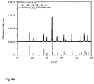
- 238000001228 spectrum Methods 0.000 description 14
- 230000005855 radiation Effects 0.000 description 12
- 239000011248 coating agent Substances 0.000 description 11
- 239000002243 precursor Substances 0.000 description 9
- 239000000919 ceramic Substances 0.000 description 8
- 239000002245 particle Substances 0.000 description 8
- 229920001296 polysiloxane Polymers 0.000 description 8
- 229910052791 calcium Inorganic materials 0.000 description 7
- 238000010438 heat treatment Methods 0.000 description 7
- LYCAIKOWRPUZTN-UHFFFAOYSA-N Ethylene glycol Chemical compound OCCO LYCAIKOWRPUZTN-UHFFFAOYSA-N 0.000 description 6
- XSQUKJJJFZCRTK-UHFFFAOYSA-N Urea Chemical compound NC(N)=O XSQUKJJJFZCRTK-UHFFFAOYSA-N 0.000 description 6
- 238000000295 emission spectrum Methods 0.000 description 6
- 239000002223 garnet Substances 0.000 description 6
- XLYOFNOQVPJJNP-UHFFFAOYSA-N water Substances O XLYOFNOQVPJJNP-UHFFFAOYSA-N 0.000 description 6
- 238000009877 rendering Methods 0.000 description 5
- 229910052712 strontium Inorganic materials 0.000 description 5
- 229910018072 Al 2 O 3 Inorganic materials 0.000 description 4
- KRKNYBCHXYNGOX-UHFFFAOYSA-K Citrate Chemical compound [O-]C(=O)CC(O)(CC([O-])=O)C([O-])=O KRKNYBCHXYNGOX-UHFFFAOYSA-K 0.000 description 4
- MUBZPKHOEPUJKR-UHFFFAOYSA-N Oxalic acid Chemical compound OC(=O)C(O)=O MUBZPKHOEPUJKR-UHFFFAOYSA-N 0.000 description 4
- 229910004298 SiO 2 Inorganic materials 0.000 description 4
- 229910010413 TiO 2 Inorganic materials 0.000 description 4
- 238000000975 co-precipitation Methods 0.000 description 4
- 238000001035 drying Methods 0.000 description 4
- 238000000695 excitation spectrum Methods 0.000 description 4
- 229910052748 manganese Inorganic materials 0.000 description 4
- 238000004519 manufacturing process Methods 0.000 description 4
- 238000003825 pressing Methods 0.000 description 4
- 229910052761 rare earth metal Inorganic materials 0.000 description 4
- 238000000985 reflectance spectrum Methods 0.000 description 4
- 238000005118 spray pyrolysis Methods 0.000 description 4
- 229910052765 Lutetium Inorganic materials 0.000 description 3
- PWHULOQIROXLJO-UHFFFAOYSA-N Manganese Chemical compound [Mn] PWHULOQIROXLJO-UHFFFAOYSA-N 0.000 description 3
- 229910002651 NO3 Inorganic materials 0.000 description 3
- NHNBFGGVMKEFGY-UHFFFAOYSA-N Nitrate Chemical compound [O-][N+]([O-])=O NHNBFGGVMKEFGY-UHFFFAOYSA-N 0.000 description 3
- GEIAQOFPUVMAGM-UHFFFAOYSA-N ZrO Inorganic materials [Zr]=O GEIAQOFPUVMAGM-UHFFFAOYSA-N 0.000 description 3
- 230000008901 benefit Effects 0.000 description 3
- 230000015572 biosynthetic process Effects 0.000 description 3
- 239000006185 dispersion Substances 0.000 description 3
- 238000005516 engineering process Methods 0.000 description 3
- 239000011521 glass Substances 0.000 description 3
- RGVLTEMOWXGQOS-UHFFFAOYSA-L manganese(2+);oxalate Chemical compound [Mn+2].[O-]C(=O)C([O-])=O RGVLTEMOWXGQOS-UHFFFAOYSA-L 0.000 description 3
- 229910052751 metal Inorganic materials 0.000 description 3
- 239000002184 metal Substances 0.000 description 3
- 229920000647 polyepoxide Polymers 0.000 description 3
- 238000001556 precipitation Methods 0.000 description 3
- 229920002050 silicone resin Polymers 0.000 description 3
- QGZKDVFQNNGYKY-UHFFFAOYSA-N Ammonia Chemical compound N QGZKDVFQNNGYKY-UHFFFAOYSA-N 0.000 description 2
- 239000004593 Epoxy Substances 0.000 description 2
- BQCADISMDOOEFD-UHFFFAOYSA-N Silver Chemical compound [Ag] BQCADISMDOOEFD-UHFFFAOYSA-N 0.000 description 2
- 238000002441 X-ray diffraction Methods 0.000 description 2
- 239000005083 Zinc sulfide Substances 0.000 description 2
- 239000012491 analyte Substances 0.000 description 2
- 239000012298 atmosphere Substances 0.000 description 2
- 229910052788 barium Inorganic materials 0.000 description 2
- 239000011230 binding agent Substances 0.000 description 2
- 239000004202 carbamide Substances 0.000 description 2
- 238000005266 casting Methods 0.000 description 2
- 238000007796 conventional method Methods 0.000 description 2
- 238000013461 design Methods 0.000 description 2
- 238000010586 diagram Methods 0.000 description 2
- 239000002019 doping agent Substances 0.000 description 2
- 238000005530 etching Methods 0.000 description 2
- 230000005284 excitation Effects 0.000 description 2
- 239000000835 fiber Substances 0.000 description 2
- 239000010408 film Substances 0.000 description 2
- 230000004907 flux Effects 0.000 description 2
- 125000000524 functional group Chemical group 0.000 description 2
- 229910052733 gallium Inorganic materials 0.000 description 2
- 239000007789 gas Substances 0.000 description 2
- 238000010348 incorporation Methods 0.000 description 2
- 238000000462 isostatic pressing Methods 0.000 description 2
- 239000010445 mica Substances 0.000 description 2
- 229910052618 mica group Inorganic materials 0.000 description 2
- 150000002910 rare earth metals Chemical class 0.000 description 2
- 239000000376 reactant Substances 0.000 description 2
- 230000009467 reduction Effects 0.000 description 2
- 238000011160 research Methods 0.000 description 2
- 229920005989 resin Polymers 0.000 description 2
- 239000011347 resin Substances 0.000 description 2
- 238000012552 review Methods 0.000 description 2
- 239000012266 salt solution Substances 0.000 description 2
- 229910052709 silver Inorganic materials 0.000 description 2
- 239000004332 silver Substances 0.000 description 2
- SQGYOTSLMSWVJD-UHFFFAOYSA-N silver(1+) nitrate Chemical compound [Ag+].[O-]N(=O)=O SQGYOTSLMSWVJD-UHFFFAOYSA-N 0.000 description 2
- 238000001694 spray drying Methods 0.000 description 2
- 239000000758 substrate Substances 0.000 description 2
- 239000000725 suspension Substances 0.000 description 2
- 238000007704 wet chemistry method Methods 0.000 description 2
- XLOMVQKBTHCTTD-UHFFFAOYSA-N zinc oxide Inorganic materials [Zn]=O XLOMVQKBTHCTTD-UHFFFAOYSA-N 0.000 description 2
- 229910052984 zinc sulfide Inorganic materials 0.000 description 2
- DRDVZXDWVBGGMH-UHFFFAOYSA-N zinc;sulfide Chemical compound [S-2].[Zn+2] DRDVZXDWVBGGMH-UHFFFAOYSA-N 0.000 description 2
- 206010001497 Agitation Diseases 0.000 description 1
- 102100032047 Alsin Human genes 0.000 description 1
- 101710187109 Alsin Proteins 0.000 description 1
- UGFAIRIUMAVXCW-UHFFFAOYSA-N Carbon monoxide Chemical compound [O+]#[C-] UGFAIRIUMAVXCW-UHFFFAOYSA-N 0.000 description 1
- BVKZGUZCCUSVTD-UHFFFAOYSA-L Carbonate Chemical compound [O-]C([O-])=O BVKZGUZCCUSVTD-UHFFFAOYSA-L 0.000 description 1
- 229910052684 Cerium Inorganic materials 0.000 description 1
- VEXZGXHMUGYJMC-UHFFFAOYSA-M Chloride anion Chemical compound [Cl-] VEXZGXHMUGYJMC-UHFFFAOYSA-M 0.000 description 1
- 229910052693 Europium Inorganic materials 0.000 description 1
- WQZGKKKJIJFFOK-GASJEMHNSA-N Glucose Natural products OC[C@H]1OC(O)[C@H](O)[C@@H](O)[C@@H]1O WQZGKKKJIJFFOK-GASJEMHNSA-N 0.000 description 1
- UFHFLCQGNIYNRP-UHFFFAOYSA-N Hydrogen Chemical compound [H][H] UFHFLCQGNIYNRP-UHFFFAOYSA-N 0.000 description 1
- 150000001169 Lutetium Chemical class 0.000 description 1
- 229910052779 Neodymium Inorganic materials 0.000 description 1
- MUBZPKHOEPUJKR-UHFFFAOYSA-L Oxalate Chemical compound [O-]C(=O)C([O-])=O MUBZPKHOEPUJKR-UHFFFAOYSA-L 0.000 description 1
- 229910004283 SiO 4 Inorganic materials 0.000 description 1
- 238000010521 absorption reaction Methods 0.000 description 1
- 239000012190 activator Substances 0.000 description 1
- 239000000654 additive Substances 0.000 description 1
- 230000000996 additive effect Effects 0.000 description 1
- 238000001856 aerosol method Methods 0.000 description 1
- AUCDRFABNLOFRE-UHFFFAOYSA-N alumane;indium Chemical compound [AlH3].[In] AUCDRFABNLOFRE-UHFFFAOYSA-N 0.000 description 1
- 229910021529 ammonia Inorganic materials 0.000 description 1
- 230000003667 anti-reflective effect Effects 0.000 description 1
- 238000013459 approach Methods 0.000 description 1
- QVGXLLKOCUKJST-UHFFFAOYSA-N atomic oxygen Chemical compound [O] QVGXLLKOCUKJST-UHFFFAOYSA-N 0.000 description 1
- WQZGKKKJIJFFOK-VFUOTHLCSA-N beta-D-glucose Chemical compound OC[C@H]1O[C@@H](O)[C@H](O)[C@@H](O)[C@@H]1O WQZGKKKJIJFFOK-VFUOTHLCSA-N 0.000 description 1
- 238000001354 calcination Methods 0.000 description 1
- 229910002091 carbon monoxide Inorganic materials 0.000 description 1
- 150000004649 carbonic acid derivatives Chemical class 0.000 description 1
- 229910010293 ceramic material Inorganic materials 0.000 description 1
- 239000003795 chemical substances by application Substances 0.000 description 1
- 238000009841 combustion method Methods 0.000 description 1
- 238000002485 combustion reaction Methods 0.000 description 1
- 230000000295 complement effect Effects 0.000 description 1
- 238000010276 construction Methods 0.000 description 1
- 239000013078 crystal Substances 0.000 description 1
- 238000005520 cutting process Methods 0.000 description 1
- 230000001419 dependent effect Effects 0.000 description 1
- 238000009792 diffusion process Methods 0.000 description 1
- 238000010616 electrical installation Methods 0.000 description 1
- 238000009429 electrical wiring Methods 0.000 description 1
- 238000005401 electroluminescence Methods 0.000 description 1
- 238000005538 encapsulation Methods 0.000 description 1
- 150000002118 epoxides Chemical class 0.000 description 1
- 239000003822 epoxy resin Substances 0.000 description 1
- 150000002148 esters Chemical class 0.000 description 1
- 238000001704 evaporation Methods 0.000 description 1
- 230000008020 evaporation Effects 0.000 description 1
- 150000004673 fluoride salts Chemical class 0.000 description 1
- 239000011888 foil Substances 0.000 description 1
- 238000009472 formulation Methods 0.000 description 1
- 238000010413 gardening Methods 0.000 description 1
- 239000008103 glucose Substances 0.000 description 1
- 150000004820 halides Chemical class 0.000 description 1
- 239000001257 hydrogen Substances 0.000 description 1
- 229910052739 hydrogen Inorganic materials 0.000 description 1
- 230000007062 hydrolysis Effects 0.000 description 1
- 238000006460 hydrolysis reaction Methods 0.000 description 1
- 238000005286 illumination Methods 0.000 description 1
- 150000002500 ions Chemical class 0.000 description 1
- 229910052746 lanthanum Inorganic materials 0.000 description 1
- 238000004020 luminiscence type Methods 0.000 description 1
- 238000002844 melting Methods 0.000 description 1
- 230000008018 melting Effects 0.000 description 1
- 238000001465 metallisation Methods 0.000 description 1
- 150000002739 metals Chemical class 0.000 description 1
- 150000002823 nitrates Chemical class 0.000 description 1
- 229910000510 noble metal Inorganic materials 0.000 description 1
- 238000005457 optimization Methods 0.000 description 1
- 230000005693 optoelectronics Effects 0.000 description 1
- 239000001301 oxygen Substances 0.000 description 1
- 229910052760 oxygen Inorganic materials 0.000 description 1
- 238000005424 photoluminescence Methods 0.000 description 1
- 239000004038 photonic crystal Substances 0.000 description 1
- 235000019353 potassium silicate Nutrition 0.000 description 1
- 230000001376 precipitating effect Effects 0.000 description 1
- 238000012545 processing Methods 0.000 description 1
- 230000001902 propagating effect Effects 0.000 description 1
- 238000010992 reflux Methods 0.000 description 1
- 150000003839 salts Chemical class 0.000 description 1
- 229910052706 scandium Inorganic materials 0.000 description 1
- SBIBMFFZSBJNJF-UHFFFAOYSA-N selenium;zinc Chemical compound [Se]=[Zn] SBIBMFFZSBJNJF-UHFFFAOYSA-N 0.000 description 1
- 230000035945 sensitivity Effects 0.000 description 1
- 238000000926 separation method Methods 0.000 description 1
- RMAQACBXLXPBSY-UHFFFAOYSA-N silicic acid Chemical class O[Si](O)(O)O RMAQACBXLXPBSY-UHFFFAOYSA-N 0.000 description 1
- 229910001961 silver nitrate Inorganic materials 0.000 description 1
- 239000002356 single layer Substances 0.000 description 1
- 239000005361 soda-lime glass Substances 0.000 description 1
- NTHWMYGWWRZVTN-UHFFFAOYSA-N sodium silicate Chemical compound [Na+].[Na+].[O-][Si]([O-])=O NTHWMYGWWRZVTN-UHFFFAOYSA-N 0.000 description 1
- 238000003980 solgel method Methods 0.000 description 1
- 239000007787 solid Substances 0.000 description 1
- 230000003595 spectral effect Effects 0.000 description 1
- 239000012798 spherical particle Substances 0.000 description 1
- 238000005507 spraying Methods 0.000 description 1
- 239000007858 starting material Substances 0.000 description 1
- CIOAGBVUUVVLOB-UHFFFAOYSA-N strontium atom Chemical compound [Sr] CIOAGBVUUVVLOB-UHFFFAOYSA-N 0.000 description 1
- GZCRRIHWUXGPOV-UHFFFAOYSA-N terbium atom Chemical compound [Tb] GZCRRIHWUXGPOV-UHFFFAOYSA-N 0.000 description 1
- 238000005979 thermal decomposition reaction Methods 0.000 description 1
- 239000010409 thin film Substances 0.000 description 1
Images


Classifications
-
- C—CHEMISTRY; METALLURGY
- C09—DYES; PAINTS; POLISHES; NATURAL RESINS; ADHESIVES; COMPOSITIONS NOT OTHERWISE PROVIDED FOR; APPLICATIONS OF MATERIALS NOT OTHERWISE PROVIDED FOR
- C09K—MATERIALS FOR MISCELLANEOUS APPLICATIONS, NOT PROVIDED FOR ELSEWHERE
- C09K11/00—Luminescent, e.g. electroluminescent, chemiluminescent materials
- C09K11/08—Luminescent, e.g. electroluminescent, chemiluminescent materials containing inorganic luminescent materials
- C09K11/77—Luminescent, e.g. electroluminescent, chemiluminescent materials containing inorganic luminescent materials containing rare earth metals
- C09K11/7766—Luminescent, e.g. electroluminescent, chemiluminescent materials containing inorganic luminescent materials containing rare earth metals containing two or more rare earth metals
- C09K11/7767—Chalcogenides
- C09K11/7769—Oxides
-
- C—CHEMISTRY; METALLURGY
- C09—DYES; PAINTS; POLISHES; NATURAL RESINS; ADHESIVES; COMPOSITIONS NOT OTHERWISE PROVIDED FOR; APPLICATIONS OF MATERIALS NOT OTHERWISE PROVIDED FOR
- C09K—MATERIALS FOR MISCELLANEOUS APPLICATIONS, NOT PROVIDED FOR ELSEWHERE
- C09K11/00—Luminescent, e.g. electroluminescent, chemiluminescent materials
- C09K11/08—Luminescent, e.g. electroluminescent, chemiluminescent materials containing inorganic luminescent materials
- C09K11/77—Luminescent, e.g. electroluminescent, chemiluminescent materials containing inorganic luminescent materials containing rare earth metals
- C09K11/7706—Aluminates
-
- C—CHEMISTRY; METALLURGY
- C09—DYES; PAINTS; POLISHES; NATURAL RESINS; ADHESIVES; COMPOSITIONS NOT OTHERWISE PROVIDED FOR; APPLICATIONS OF MATERIALS NOT OTHERWISE PROVIDED FOR
- C09K—MATERIALS FOR MISCELLANEOUS APPLICATIONS, NOT PROVIDED FOR ELSEWHERE
- C09K11/00—Luminescent, e.g. electroluminescent, chemiluminescent materials
- C09K11/08—Luminescent, e.g. electroluminescent, chemiluminescent materials containing inorganic luminescent materials
- C09K11/59—Luminescent, e.g. electroluminescent, chemiluminescent materials containing inorganic luminescent materials containing silicon
-
- C—CHEMISTRY; METALLURGY
- C09—DYES; PAINTS; POLISHES; NATURAL RESINS; ADHESIVES; COMPOSITIONS NOT OTHERWISE PROVIDED FOR; APPLICATIONS OF MATERIALS NOT OTHERWISE PROVIDED FOR
- C09K—MATERIALS FOR MISCELLANEOUS APPLICATIONS, NOT PROVIDED FOR ELSEWHERE
- C09K11/00—Luminescent, e.g. electroluminescent, chemiluminescent materials
- C09K11/08—Luminescent, e.g. electroluminescent, chemiluminescent materials containing inorganic luminescent materials
- C09K11/70—Luminescent, e.g. electroluminescent, chemiluminescent materials containing inorganic luminescent materials containing phosphorus
- C09K11/71—Luminescent, e.g. electroluminescent, chemiluminescent materials containing inorganic luminescent materials containing phosphorus also containing alkaline earth metals
-
- C—CHEMISTRY; METALLURGY
- C09—DYES; PAINTS; POLISHES; NATURAL RESINS; ADHESIVES; COMPOSITIONS NOT OTHERWISE PROVIDED FOR; APPLICATIONS OF MATERIALS NOT OTHERWISE PROVIDED FOR
- C09K—MATERIALS FOR MISCELLANEOUS APPLICATIONS, NOT PROVIDED FOR ELSEWHERE
- C09K11/00—Luminescent, e.g. electroluminescent, chemiluminescent materials
- C09K11/08—Luminescent, e.g. electroluminescent, chemiluminescent materials containing inorganic luminescent materials
- C09K11/77—Luminescent, e.g. electroluminescent, chemiluminescent materials containing inorganic luminescent materials containing rare earth metals
- C09K11/7701—Chalogenides
- C09K11/7703—Chalogenides with alkaline earth metals
-
- C—CHEMISTRY; METALLURGY
- C09—DYES; PAINTS; POLISHES; NATURAL RESINS; ADHESIVES; COMPOSITIONS NOT OTHERWISE PROVIDED FOR; APPLICATIONS OF MATERIALS NOT OTHERWISE PROVIDED FOR
- C09K—MATERIALS FOR MISCELLANEOUS APPLICATIONS, NOT PROVIDED FOR ELSEWHERE
- C09K11/00—Luminescent, e.g. electroluminescent, chemiluminescent materials
- C09K11/08—Luminescent, e.g. electroluminescent, chemiluminescent materials containing inorganic luminescent materials
- C09K11/77—Luminescent, e.g. electroluminescent, chemiluminescent materials containing inorganic luminescent materials containing rare earth metals
- C09K11/7766—Luminescent, e.g. electroluminescent, chemiluminescent materials containing inorganic luminescent materials containing rare earth metals containing two or more rare earth metals
- C09K11/7774—Aluminates
-
- H—ELECTRICITY
- H05—ELECTRIC TECHNIQUES NOT OTHERWISE PROVIDED FOR
- H05B—ELECTRIC HEATING; ELECTRIC LIGHT SOURCES NOT OTHERWISE PROVIDED FOR; CIRCUIT ARRANGEMENTS FOR ELECTRIC LIGHT SOURCES, IN GENERAL
- H05B33/00—Electroluminescent light sources
- H05B33/12—Light sources with substantially two-dimensional radiating surfaces
- H05B33/14—Light sources with substantially two-dimensional radiating surfaces characterised by the chemical or physical composition or the arrangement of the electroluminescent material, or by the simultaneous addition of the electroluminescent material in or onto the light source
-
- H—ELECTRICITY
- H10—SEMICONDUCTOR DEVICES; ELECTRIC SOLID-STATE DEVICES NOT OTHERWISE PROVIDED FOR
- H10H—INORGANIC LIGHT-EMITTING SEMICONDUCTOR DEVICES HAVING POTENTIAL BARRIERS
- H10H20/00—Individual inorganic light-emitting semiconductor devices having potential barriers, e.g. light-emitting diodes [LED]
- H10H20/80—Constructional details
- H10H20/85—Packages
- H10H20/851—Wavelength conversion means
- H10H20/8511—Wavelength conversion means characterised by their material, e.g. binder
- H10H20/8512—Wavelength conversion materials
Definitions
- the invention relates to Mn 4+ -activated phosphors, processes for the preparation of these compounds and their use as conversion phosphors or in illuminants.
- Luminescent materials are used in fluorescent light sources, emissive screens and as scintillator crystals for the conversion of non-visible radiation or high energy particles into visible light.
- a class of materials that has become widely used for this task are the Ce 3+ doped garnets, in particular Y 3 Al 5 O 12 : Ce (YAG) and (Gd 1-x Y x ) 3 (Al 1-y Ga y ) 5 O 12: Ce (YAGaG: Ce), said other dopants such as Lu 3+ or Tb 3+ were used for the optimization of the spectrum.
- white LEDs were realized by the partial conversion of the blue light with YAG: Ce or YAGaG: Ce, because the yellow-orange emission color of these phosphors is complementary to the blue emission color of the LEDs, and thus additive white light can be obtained.
- all commercially available white LEDs contain a blue-emitting InGaN chip covered with a layer of YAG: Ce or YAGaG: Ce.
- Significant disadvantages of this approach is, on the one hand, the dependence of the emission color on the viewing angle, which is a consequence of the non-homogeneous coating of the chip.
- the current primary goal for extending the product range and improving the color rendering of white LEDs is the realization of trichromatic LEDs.
- green or yellow and red-emitting phosphors with high absorption in the blue spectral range, with high quantum efficiency and a high lumen equivalent must be provided.
- red-emitting phosphors such as (Ca, Sr) S: Eu, (Ca, Sr, Ba) 2 Si 5 N 8 : Eu and (Ca, Sr) AlSiN 3 : Eu or mixtures of these luminophores were already proposed in a variety of patent applications.
- a disadvantage of the previously used red emitting phosphors is their relatively low stability, which is due in part to the susceptibility to hydrolysis of the sulfidic or nitridic host lattices and partly to the redox lability of the Eu 2+ activator.
- the lumen equivalent of 200-270 lm / W is not as high as that of Eu 3+ phosphors with 280-360 lm / W due to the broad emission band. Therefore, the search for efficient and stable red-emitting phosphors for LEDs with high lumen equivalent continues unabated.
- garnet phosphors of the rare earth metals of the general type (Gd, Tb, La, Lu, Y) 3 (Al, Ga) 5 O 12 : (Ce, Eu, Nd, Er, Cr, Mn) are known.
- Garnet phosphors according to the present invention containing both manganese and calcium are not disclosed.
- garnet phosphors of the rare earth metals of the general type (Y, Gd, Lu, Tb) 3 (Al, Ga) 5 O 12 : Ce are known.
- Garnet phosphors according to the present invention containing both manganese and calcium are not disclosed.
- Object of the present invention was to develop lutetium-containing garnet phosphors, which have a red luminescence and Particularly suitable for use in high-performance pcLEDs for producing warm white light.
- Mn 4+ -activated lutetium-containing garnet phosphors fulfill the abovementioned object.
- the incorporation of tetravalent manganese in the lattice site of the trivalent aluminum must be compensated by the incorporation of a divalent ion, such as Ca 2+ or Sr 2+ on the Lu 3+ place.
- x is a value in the range 0 to 2.0 and particularly preferably in the range 0.10 to 0.90.
- y is a value from the range 0.10 to 0.45, particularly preferably from the range 0.20 to 0.40.
- LED quality is described using common parameters, such as the Color Rendering Index or the color point in CIE x and CIE y coordinates.
- the Color Rendering Index is a unitary photometric quantity known to those skilled in the art that compares the color fidelity of an artificial light source to that of sunlight or filament light sources (the latter two have a CRI of 100).
- CIE x and CIE y stand for the coordinates in the CIE standard color diagram familiar to the person skilled in the art (here standard observer 1931), with which the color of a light source is described. All the variables listed above are calculated from emission spectra of the light source according to methods familiar to the person skilled in the art.
- red light such light whose intensity maximum is between 600 and 680 nm wavelength.
- the reaction is usually carried out at a temperature above 800 ° C.
- the calcination may also be carried out under reducing conditions (e.g., with carbon monoxide, forming gas or hydrogen or oxygen depleted atmosphere).
- An inorganic or organic substance is a substance from the group of ammonium halides, alkaline earth fluorides such as calcium, strontium or barium fluoride, (earth) alkali metal borates, boric acid, (earth) alkali metal carbonates or ammonium bicarbonate, Citric acid, alcoholates and oxalates and / or silicic acid esters such as TEOS used.
- alkaline earth fluorides such as calcium, strontium or barium fluoride
- boric acid earth alkali metal carbonates or ammonium bicarbonate
- Citric acid e.g., citric acid and an oxalate are added.
- the oxalate may also be added in step a).
- the phosphors according to the invention can be prepared either by a conventional solid-state diffusion method (starting from the oxides, nitrates, carbonates or halides of the corresponding alkaline earth metals, semimetals, metals or rare earths) or wet-chemically from inorganic and / or organic metal and / or rare earth salts by means of sol Gel process, coprecipitation and / or drying process.
- a conventional solid-state diffusion method starting from the oxides, nitrates, carbonates or halides of the corresponding alkaline earth metals, semimetals, metals or rare earths
- wet-chemically from inorganic and / or organic metal and / or rare earth salts by means of sol Gel process, coprecipitation and / or drying process.
- wet-chemical processes particularly preferably wet-chemical by the addition of citric acid.
- chloride solutions of the corresponding phosphor educts are admixed with a TEOS / NH 4 HCO 3 solution, whereby the phosphor precursor is formed, which is subsequently converted into the phosphor by a one-stage or multistage thermal treatment.
- Spray pyrolysis belongs to the aerosol processes which are characterized by spraying solutions, suspensions or dispersions into a reaction chamber (reactor) which has been heated in different ways, as well as the formation and separation of solid particles.
- spray pyrolysis as the high-temperature process is characterized by the thermal decomposition of the educts used (eg salts) and the formation of new substances (eg oxides, mixed oxides ) instead of.
- the orange-red emitting phosphors of the present invention may also be mixed with green emitting phosphors, making such blends highly suitable for general lighting applications (e.g., warm white LEDs) and LCD backlighting.
- a further embodiment of the present invention is therefore a mixture comprising at least one compound of the formula I and at least one green-emitting phosphor, which is preferably selected from Ce-doped garnets, preferably LuAG: Ce, (Sr, Ca) Si 2 N 2 O 2 : Eu, (Sr, Ba) 2 SiO 4 : Eu, or CaSc 2 O 4 : Ce, Na.
- Ce-doped garnets preferably LuAG: Ce, (Sr, Ca) Si 2 N 2 O 2 : Eu, (Sr, Ba) 2 SiO 4 : Eu, or CaSc 2 O 4 : Ce, Na.
- the compound (or phosphor) according to formula I and the at least one green emitting phosphor are usually present in a weight ratio of 20: 1 to 1: 1. It is preferred according to the invention for the at least one phosphor of the formula I and the at least one green-emitting phosphor to be present in a weight ratio of 10: 1 to 3: 1 and particularly preferably 6: 1 to 4: 1.
- the particle size of the phosphors according to the invention is usually between 50 nm and 30 .mu.m, preferably between 1 .mu.m and 20 .mu.m.
- the phosphors in particle form have a closed surface coating consisting of SiO 2 , TiO 2 , Al 2 O 3 , ZnO, ZrO 2 and / or Y 2 O 3 or mixed oxides thereof.
- This surface coating has the advantage that by a suitable Grading the refractive indices of the coating materials, an adjustment of the refractive index can be achieved with the environment. In this case, the scattering of the light at the surface of the phosphor is reduced and a larger proportion of the light can penetrate into the phosphor where it is absorbed and converted.
- the refractive index matched surface coating allows more light to be coupled out of the phosphor because the total internal reflection is reduced.
- a closed layer is advantageous if the phosphor has to be encapsulated. This may be necessary to counter sensitivity of the phosphor or parts thereof to diffusing water or other materials in the immediate environment. Another reason for the encapsulation with a closed shell is a thermal decoupling of the actual phosphor from the heat that arises in the chip. This heat leads to a reduction in the fluorescent light output of the phosphor and may also affect the color of the fluorescent light. Finally, it is possible by such a coating to increase the efficiency of the phosphor by preventing lattice vibrations arising in the phosphor from propagating to the environment.
- the phosphors have a porous surface coating consisting of SiO 2 , TiO 2 , Al 2 O 3 , ZnO, ZrO 2 and / or Y 2 O 3 or mixed oxides thereof or of the phosphor composition.
- These porous coatings offer the possibility of further reducing the refractive index of a single layer.
- the preparation of such porous coatings can be accomplished by three conventional methods as described in US Pat WO 03/027015 which is fully incorporated by reference into the context of the present application: the etching of glass (eg Soda lime glasses (see US 4,019,884 )), the application of a porous layer and the combination of porous layer and an etching process.
- the phosphor particles have a surface which carries functional groups which allow a chemical connection to the environment, preferably consisting of epoxy or silicone resin.
- functional groups may e.g. oxo group-attached esters or other derivatives which can form linkages with components based on epoxides and / or silicones.
- Such surfaces have the advantage that a homogeneous mixing of the phosphors is made possible in the binder.
- the rheological properties of the system phosphor / binder and also the pot life can be adjusted to a certain extent. This simplifies the processing of the mixtures.
- the phosphor layer applied to an LED chip preferably consists of a mixture of silicone and homogeneous phosphor particles, which is applied by volume casting, and the silicone has a surface tension, this phosphor layer is not uniform at the microscopic level or the thickness of the layer is not consistently constant , This is usually also the case when the phosphor is not applied by the volume casting method, but in the so-called chip-level conversion method in which a highly concentrated, thin phosphor layer is applied directly to the surface of the chip by means of electrostatic methods.
- any external forms of the phosphor particles such as spherical particles, platelets and structured materials and ceramics.
- platelet-shaped phosphors as a further preferred embodiment is done by conventional methods from the corresponding metal and / or rare earth salts.
- the production process is in EP 763573 and DE 102006054331 described in detail which are fully incorporated by reference into the context of the present application.
- These platelet-shaped phosphors can be prepared by a natural or synthetically produced highly stable support or a substrate of, for example mica, SiO 2 , Al 2 O 3 , ZrO 2 , glass or TiO 2 platelets, which is a very has high aspect ratio, has an atomically smooth surface and an adjustable thickness, can be coated by precipitation reaction in aqueous dispersion or suspension with a phosphor layer.
- the platelets may also consist of the phosphor material itself, or be constructed of a different material. If the wafer itself merely serves as a carrier for the phosphor coating, it must be made of a material which is transparent to the primary radiation of the LED, or absorbs the primary radiation and transfers this energy to the phosphor layer.
- the platelet-shaped phosphors are dispersed in a resin (eg, silicone or epoxy resin), and this dispersion is applied to the LED chip.
- the platelet-shaped phosphors can be produced on a large scale in thicknesses of 50 nm up to about 20 ⁇ m, preferably between 150 nm and 5 ⁇ m.
- the diameter is from 50 nm to 20 microns. It usually has an aspect ratio (ratio of diameter to particle thickness) of 1: 1 to 400: 1, and in particular 3: 1 to 100: 1.
- the platelet expansion (length x width) depends on the arrangement. Platelets are also suitable as scattering centers within the conversion layer, especially if they have particularly small dimensions.
- the surface of the platelet-shaped phosphor according to the invention facing the LED chip can be provided with a coating which is anti-reflective with respect to the primary radiation emitted by the LED chip.
- the production of the phosphors according to the invention in the form of ceramic bodies is carried out analogously to that in the DE 102006037730 (Merck), which is fully incorporated by reference into the context of the present application.
- the phosphor is prepared wet-chemically by mixing the corresponding reactants and dopants, then isostatically pressed and applied in the form of a homogeneous thin and non-porous platelets directly on the surface of the chip.
- no location-dependent variation of the excitation and emission of the phosphor takes place, as a result of which the LED equipped with it emits a homogeneous and color-constant light cone and has a high light output.
- the ceramic phosphor bodies can be produced industrially, for example, as platelets in thicknesses of a few 100 nm up to about 500 ⁇ m.
- the platelet extent (length x width) depends on the arrangement.
- the size of the wafer according to the chip size (from about 100 .mu.m * 100 microns to several mm 2 ) with a certain excess of about 10% - 30% of the chip surface with a suitable chip arrangement (eg Flip Chip arrangement) or to choose accordingly.
- a suitable chip arrangement eg Flip Chip arrangement
- the side surfaces of the ceramic phosphor body can be mirrored with a light or noble metal, preferably aluminum or silver.
- the mirroring causes no light to emerge laterally from the phosphor body. Lateral exiting light can reduce the luminous flux to be coupled out of the LED.
- the mirroring of the ceramic phosphor body is carried out in a process step after the isostatic pressing to rods or plates, which may be done before the mirroring cutting the rods or plates into the required size.
- the side surfaces are wetted, for example, with a solution of silver nitrate and glucose, and then exposed to an ammonia atmosphere at elevated temperature.
- an ammonia atmosphere at elevated temperature.
- electroless metallization offer, see for example Hollemann-Wiberg, Textbook of Inorganic Chemistry, Walter de Gruyter Verlag or Ullmann's Encyclopedia of Chemical Technology.
- the ceramic phosphor body can, if necessary, be fixed with a water glass solution on the substrate of an LED chip.
- the ceramic phosphor body has a structured (eg pyramidal) surface on the side opposite an LED chip.
- the structured surface on the phosphor body is produced in that in the isostatic pressing, the pressing tool has a structured pressing plate and thereby embossed a structure in the surface. Structured surfaces are desired when thin phosphor bodies or platelets are to be produced.
- the pressing conditions are known to the person skilled in the art (see J. warrior, Technical Ceramic Materials, Chap. 4, German Economic Service, 1998 ). It is important that 2/3 to 5/6 of the melting temperature of the material to be pressed are used as pressing temperatures.
- the excitability of the phosphors according to the invention also extends over a wide range, ranging from about 410 nm to 530 nm, preferably 430 nm to about 500 nm.
- these phosphors are not only suitable for excitation by violet or blue emitting light sources such as LEDs or conventional discharge lamps (eg based on Hg), but also for light sources such as those which exploit the blue In 3+ line at 451 nm.
- Another object of the present invention is a light source, characterized in that it contains a semiconductor and at least one compound or a phosphor according to formula I.
- Another object of the present invention is a light source characterized in that it contains a semiconductor and at least one compound of formula I and at least one green-emitting phosphor.
- this lighting unit emits white or emits light with a certain color point (color-on-demand principle).
- This concept is e.g. used to design certain corporate designs, e.g. for illuminated company logos, brands etc.
- the light source is a luminescent arrangement based on ZnO, TCO (transparent conducting oxide), ZnSe or SiC or else an arrangement based on an organic light-emitting layer (OLED).
- ZnO transparent conducting oxide
- ZnSe transparent conducting oxide
- SiC organic light-emitting layer
- the light source is a source which exhibits electroluminescence and / or photoluminescence.
- the light source may also be a plasma or discharge source.
- the phosphors according to the invention can either be dispersed in a resin (for example epoxy or silicone resin) or, with suitable size ratios, be arranged directly on the light source or can be arranged remotely therefrom, depending on the application (the latter arrangement also includes “remote phosphor technology”). with a).
- a resin for example epoxy or silicone resin
- the advantages of "remote phosphor technology” are known to the person skilled in the art and can be found, for example, in the following publication: Japanese Journal. of Appl. Phys. Vol. 44, no. 21 (2005) L649-L651 ,
- a lighting unit in particular for the backlight of display devices, which is characterized in that it contains at least one light source described above and corresponding display devices, in particular Liquid crystal display device (LC display), with a backlight, characterized in that they contain at least one such lighting unit.
- LC display Liquid crystal display device
- CRI values> 85 can only be realized if the red phosphor according to the invention according to formula I is additionally combined with green phosphors in the LED.
- the optical coupling of the illumination unit between the phosphor and the semiconductor is realized by a light-conducting arrangement.
- the semiconductor is installed at a central location and this is optically coupled to the phosphor by means of light-conducting devices, such as, for example, photoconductive fibers.
- the lighting requirements adapted lights can only be realized consisting of one or different phosphors, which can be arranged to form a luminescent screen, and a light guide, which is coupled to the light source.
- a strong light source at a convenient location for the electrical installation and to install without further electrical wiring, but only by laying fiber optics at any location lights of phosphors, which are coupled to the light guide.
- Another object of the present invention is the use of the phosphors according to the invention for the partial or complete conversion of blue or in the near UV emission of a light-emitting diode.
- the use of the phosphors according to the invention for the conversion of blue or near-UV emission into visible white radiation is preferred. Furthermore, the use of the phosphors according to the invention for converting the primary radiation into a specific color point according to the "color on demand" concept is preferred.
- Another object of the present invention is the use of the phosphors according to the invention in electroluminescent materials, such as electroluminescent films (also called phosphors or light foils) in which, for example, zinc sulfide or zinc sulfide doped with Mn 2+ , Cu + , or Ag + as an emitter is used, which emit in the yellow-green area.
- electroluminescent materials such as electroluminescent films (also called phosphors or light foils) in which, for example, zinc sulfide or zinc sulfide doped with Mn 2+ , Cu + , or Ag + as an emitter is used, which emit in the yellow-green area.
- the fields of application of the electroluminescent film are, for example, advertising, display backlighting in liquid crystal displays (LC displays) and thin-film transistor displays (TFT displays), self-illuminating license plate labels, floor graphics (in conjunction with a non-slip and non-slip laminate), in display and / or controls for example in automobiles, trains, ships and aircraft or household, gardening, measuring or sports and leisure equipment.
- LC displays liquid crystal displays
- TFT displays thin-film transistor displays
- license plate labels in conjunction with a non-slip and non-slip laminate
- floor graphics in conjunction with a non-slip and non-slip laminate
- a phosphor from Examples 1 to 4 is mixed in a tumble mixer with a 2-component silicone (OE6550 Fa. Dow Corning), so that equal amounts of the phosphor are dispersed in the two components of the silicone, the total concentration of the phosphor mixture in the silicone 8% by weight.
- a 2-component silicone OE6550 Fa. Dow Corning
- CIE x and CIE y represent the coordinates in the CIE standard color diagram familiar to the person skilled in the art (here standard observer 1931), which describes the color of a light source. All the variables listed above are calculated from emission spectra of the light source according to methods familiar to the person skilled in the art.
Landscapes
- Chemical & Material Sciences (AREA)
- Inorganic Chemistry (AREA)
- Engineering & Computer Science (AREA)
- Materials Engineering (AREA)
- Organic Chemistry (AREA)
- Luminescent Compositions (AREA)
- Inorganic Compounds Of Heavy Metals (AREA)
- Planar Illumination Modules (AREA)
Applications Claiming Priority (2)
| Application Number | Priority Date | Filing Date | Title |
|---|---|---|---|
| DE102010047474A DE102010047474A1 (de) | 2010-10-06 | 2010-10-06 | Mn-aktivierte Leuchtstoffe |
| PCT/EP2011/004652 WO2012045393A1 (de) | 2010-10-06 | 2011-09-16 | Mn-aktivierte leuchtstoffe |
Publications (2)
| Publication Number | Publication Date |
|---|---|
| EP2625247A1 EP2625247A1 (de) | 2013-08-14 |
| EP2625247B1 true EP2625247B1 (de) | 2016-11-30 |
Family
ID=44677842
Family Applications (1)
| Application Number | Title | Priority Date | Filing Date |
|---|---|---|---|
| EP11761009.7A Not-in-force EP2625247B1 (de) | 2010-10-06 | 2011-09-16 | Mn-aktivierte leuchtstoffe |
Country Status (7)
Families Citing this family (7)
| Publication number | Priority date | Publication date | Assignee | Title |
|---|---|---|---|---|
| WO2014177247A1 (de) * | 2013-05-02 | 2014-11-06 | Merck Patent Gmbh | Leuchtstoffe |
| KR102355081B1 (ko) | 2014-12-26 | 2022-01-26 | 삼성전자주식회사 | 불화물 형광체 제조방법, 백색 발광장치, 디스플레이 장치 및 조명장치 |
| US10486171B2 (en) | 2015-06-29 | 2019-11-26 | Dow Global Technologies Llc | Process for producing flexible container with microcapillary dispensing system |
| CN105331364B (zh) * | 2015-10-12 | 2017-09-05 | 杭州电子科技大学 | 一种YAG:Mn红色荧光粉以及其制备方法和应用 |
| DE102015015355A1 (de) | 2015-12-01 | 2017-06-01 | Merck Patent Gmbh | Mn-aktivierte Leuchtstoffe |
| WO2017199142A1 (en) * | 2016-05-20 | 2017-11-23 | Semiconductor Energy Laboratory Co., Ltd. | Light-emitting device and electronic device |
| CN117865667A (zh) * | 2023-12-25 | 2024-04-12 | 江苏锡沂高新材料产业技术研究院有限公司 | 一种采用同步沉淀方式制备yag基透明陶瓷的方法 |
Family Cites Families (15)
| Publication number | Priority date | Publication date | Assignee | Title |
|---|---|---|---|---|
| US4019884A (en) | 1976-01-22 | 1977-04-26 | Corning Glass Works | Method for providing porous broad-band antireflective surface layers on chemically-durable borosilicate glasses |
| NL181063C (nl) * | 1976-05-13 | 1987-06-01 | Philips Nv | Luminescerend scherm; lagedrukkwikdampontladingslamp; werkwijze voor de bereiding van een luminescerend materiaal. |
| NL7700419A (nl) * | 1977-01-17 | 1978-07-19 | Philips Nv | Magnetisch beldomein materiaal. |
| JP3242561B2 (ja) | 1995-09-14 | 2001-12-25 | メルク・ジヤパン株式会社 | 薄片状酸化アルミニウム、真珠光沢顔料及びその製造方法 |
| US6556336B2 (en) * | 1997-07-24 | 2003-04-29 | Scientific Materials, Corp. | Optical laser light limiter |
| DE29820384U1 (de) * | 1998-11-06 | 1999-01-14 | Opto-System GmbH, 12555 Berlin | Leucht- oder Anzeigeelement mit mischfarbigen, insbesondere weißem Licht |
| US7241505B2 (en) | 2001-09-21 | 2007-07-10 | Merck Patent, Gmbh | Hybrid sol for the production of abrasion-resistant SiO2 antireflection coatings |
| DE10213294B4 (de) | 2002-03-25 | 2015-05-13 | Osram Gmbh | Verwendung eines UV-beständigen Polymers in der Optoelektronik sowie im Außenanwendungsbereich, UV-beständiges Polymer sowie optisches Bauelement |
| CN1255506C (zh) * | 2003-11-13 | 2006-05-10 | 北京有色金属研究总院 | 含硼的白光led用荧光粉及其制造方法和所制成的电光源 |
| DE102006027306B4 (de) * | 2006-06-06 | 2013-10-17 | Schott Ag | Verfahren zur Herstellung einer Glaskeramik mit einer Granatphase und Verwendung der danach hergestellten Glaskeramik |
| DE102006027133A1 (de) | 2006-06-12 | 2007-12-13 | Merck Patent Gmbh | Verfahren zur Herstellung von Granat-Leuchtstoffen in einem Pulsationsreaktor |
| DE102006037730A1 (de) | 2006-08-11 | 2008-02-14 | Merck Patent Gmbh | LED-Konversionsleuchtstoffe in Form von keramischen Körpern |
| DE102006054331A1 (de) | 2006-11-17 | 2008-05-21 | Merck Patent Gmbh | Leuchtstoffkörper basierend auf plättchenförmigen Substraten |
| US9133392B2 (en) * | 2010-07-22 | 2015-09-15 | Osram Opto Semiconductors Gmbh | Garnet material, method for its manufacturing and radiation-emitting component comprising the garnet material |
| TWI486254B (zh) * | 2010-09-20 | 2015-06-01 | Nitto Denko Corp | 發光陶瓷層板及其製造方法 |
-
2010
- 2010-10-06 DE DE102010047474A patent/DE102010047474A1/de not_active Withdrawn
-
2011
- 2011-09-16 EP EP11761009.7A patent/EP2625247B1/de not_active Not-in-force
- 2011-09-16 WO PCT/EP2011/004652 patent/WO2012045393A1/de active Application Filing
- 2011-09-16 CN CN2011800481843A patent/CN103154196A/zh active Pending
- 2011-09-16 KR KR1020137011771A patent/KR20130111562A/ko not_active Abandoned
- 2011-09-16 US US13/877,954 patent/US9080104B2/en not_active Expired - Fee Related
- 2011-09-16 JP JP2013532060A patent/JP5912121B2/ja not_active Expired - Fee Related
Also Published As
| Publication number | Publication date |
|---|---|
| CN103154196A (zh) | 2013-06-12 |
| EP2625247A1 (de) | 2013-08-14 |
| JP5912121B2 (ja) | 2016-04-27 |
| WO2012045393A1 (de) | 2012-04-12 |
| US9080104B2 (en) | 2015-07-14 |
| US20130193472A1 (en) | 2013-08-01 |
| KR20130111562A (ko) | 2013-10-10 |
| JP2014502243A (ja) | 2014-01-30 |
| DE102010047474A1 (de) | 2012-04-12 |
Similar Documents
| Publication | Publication Date | Title |
|---|---|---|
| EP2616523B1 (de) | Silicophosphat-leuchtstoffe | |
| EP2576725B1 (de) | Leuchtstoffe | |
| EP2129740B1 (de) | Verfahren zur herstellung von leuchtstoffen basierend auf orthosilikaten für pcleds | |
| EP2115092B1 (de) | Leuchtstoffe bestehend aus dotierten granaten für pcleds | |
| EP2596078B1 (de) | Aluminat-leuchtstoffe | |
| EP2129741B1 (de) | VERFAHREN ZUR HERSTELLUNG VON LEUCHTSTOFFEN BESTEHEND AUS ORTHOSILIKATEN FÜR pcLEDs | |
| EP2914688B1 (de) | Eu-aktivierte leuchtstoffe | |
| WO2010043287A1 (de) | Dotierte granat-leuchtstoffe mit rotverschiebung für pcleds | |
| EP2625247B1 (de) | Mn-aktivierte leuchtstoffe | |
| EP2324096B1 (de) | Co-dotierte 1-1-2 nitride | |
| DE102009032711A1 (de) | Co-dotierte Silicooxynitride | |
| EP2596681B1 (de) | Carbodiimid-leuchtstoffe | |
| DE102009050542A1 (de) | Sm-aktivierte Aluminat- und Borat-Leuchtstoffe | |
| EP2619283B1 (de) | Silicat-leuchtstoffe |
Legal Events
| Date | Code | Title | Description |
|---|---|---|---|
| PUAI | Public reference made under article 153(3) epc to a published international application that has entered the european phase |
Free format text: ORIGINAL CODE: 0009012 |
|
| 17P | Request for examination filed |
Effective date: 20130305 |
|
| AK | Designated contracting states |
Kind code of ref document: A1 Designated state(s): AL AT BE BG CH CY CZ DE DK EE ES FI FR GB GR HR HU IE IS IT LI LT LU LV MC MK MT NL NO PL PT RO RS SE SI SK SM TR |
|
| RIN1 | Information on inventor provided before grant (corrected) |
Inventor name: BLEISE, ANDRE Inventor name: WINKLER, HOLGER Inventor name: JUESTEL, THOMAS |
|
| DAX | Request for extension of the european patent (deleted) | ||
| 17Q | First examination report despatched |
Effective date: 20140317 |
|
| GRAP | Despatch of communication of intention to grant a patent |
Free format text: ORIGINAL CODE: EPIDOSNIGR1 |
|
| RIC1 | Information provided on ipc code assigned before grant |
Ipc: C09K 11/77 20060101AFI20160620BHEP Ipc: H01L 33/50 20100101ALI20160620BHEP |
|
| INTG | Intention to grant announced |
Effective date: 20160706 |
|
| GRAS | Grant fee paid |
Free format text: ORIGINAL CODE: EPIDOSNIGR3 |
|
| GRAA | (expected) grant |
Free format text: ORIGINAL CODE: 0009210 |
|
| AK | Designated contracting states |
Kind code of ref document: B1 Designated state(s): AL AT BE BG CH CY CZ DE DK EE ES FI FR GB GR HR HU IE IS IT LI LT LU LV MC MK MT NL NO PL PT RO RS SE SI SK SM TR |
|
| REG | Reference to a national code |
Ref country code: CH Ref legal event code: EP Ref country code: GB Ref legal event code: FG4D Free format text: NOT ENGLISH |
|
| REG | Reference to a national code |
Ref country code: AT Ref legal event code: REF Ref document number: 849797 Country of ref document: AT Kind code of ref document: T Effective date: 20161215 |
|
| REG | Reference to a national code |
Ref country code: IE Ref legal event code: FG4D Free format text: LANGUAGE OF EP DOCUMENT: GERMAN |
|
| REG | Reference to a national code |
Ref country code: DE Ref legal event code: R096 Ref document number: 502011011258 Country of ref document: DE |
|
| PG25 | Lapsed in a contracting state [announced via postgrant information from national office to epo] |
Ref country code: LV Free format text: LAPSE BECAUSE OF FAILURE TO SUBMIT A TRANSLATION OF THE DESCRIPTION OR TO PAY THE FEE WITHIN THE PRESCRIBED TIME-LIMIT Effective date: 20161130 |
|
| REG | Reference to a national code |
Ref country code: LT Ref legal event code: MG4D |
|
| REG | Reference to a national code |
Ref country code: NL Ref legal event code: MP Effective date: 20161130 |
|
| PG25 | Lapsed in a contracting state [announced via postgrant information from national office to epo] |
Ref country code: NO Free format text: LAPSE BECAUSE OF FAILURE TO SUBMIT A TRANSLATION OF THE DESCRIPTION OR TO PAY THE FEE WITHIN THE PRESCRIBED TIME-LIMIT Effective date: 20170228 Ref country code: LT Free format text: LAPSE BECAUSE OF FAILURE TO SUBMIT A TRANSLATION OF THE DESCRIPTION OR TO PAY THE FEE WITHIN THE PRESCRIBED TIME-LIMIT Effective date: 20161130 Ref country code: SE Free format text: LAPSE BECAUSE OF FAILURE TO SUBMIT A TRANSLATION OF THE DESCRIPTION OR TO PAY THE FEE WITHIN THE PRESCRIBED TIME-LIMIT Effective date: 20161130 Ref country code: GR Free format text: LAPSE BECAUSE OF FAILURE TO SUBMIT A TRANSLATION OF THE DESCRIPTION OR TO PAY THE FEE WITHIN THE PRESCRIBED TIME-LIMIT Effective date: 20170301 |
|
| PG25 | Lapsed in a contracting state [announced via postgrant information from national office to epo] |
Ref country code: HR Free format text: LAPSE BECAUSE OF FAILURE TO SUBMIT A TRANSLATION OF THE DESCRIPTION OR TO PAY THE FEE WITHIN THE PRESCRIBED TIME-LIMIT Effective date: 20161130 Ref country code: ES Free format text: LAPSE BECAUSE OF FAILURE TO SUBMIT A TRANSLATION OF THE DESCRIPTION OR TO PAY THE FEE WITHIN THE PRESCRIBED TIME-LIMIT Effective date: 20161130 Ref country code: RS Free format text: LAPSE BECAUSE OF FAILURE TO SUBMIT A TRANSLATION OF THE DESCRIPTION OR TO PAY THE FEE WITHIN THE PRESCRIBED TIME-LIMIT Effective date: 20161130 Ref country code: PL Free format text: LAPSE BECAUSE OF FAILURE TO SUBMIT A TRANSLATION OF THE DESCRIPTION OR TO PAY THE FEE WITHIN THE PRESCRIBED TIME-LIMIT Effective date: 20161130 Ref country code: PT Free format text: LAPSE BECAUSE OF FAILURE TO SUBMIT A TRANSLATION OF THE DESCRIPTION OR TO PAY THE FEE WITHIN THE PRESCRIBED TIME-LIMIT Effective date: 20170330 Ref country code: FI Free format text: LAPSE BECAUSE OF FAILURE TO SUBMIT A TRANSLATION OF THE DESCRIPTION OR TO PAY THE FEE WITHIN THE PRESCRIBED TIME-LIMIT Effective date: 20161130 |
|
| PG25 | Lapsed in a contracting state [announced via postgrant information from national office to epo] |
Ref country code: NL Free format text: LAPSE BECAUSE OF FAILURE TO SUBMIT A TRANSLATION OF THE DESCRIPTION OR TO PAY THE FEE WITHIN THE PRESCRIBED TIME-LIMIT Effective date: 20161130 |
|
| PG25 | Lapsed in a contracting state [announced via postgrant information from national office to epo] |
Ref country code: RO Free format text: LAPSE BECAUSE OF FAILURE TO SUBMIT A TRANSLATION OF THE DESCRIPTION OR TO PAY THE FEE WITHIN THE PRESCRIBED TIME-LIMIT Effective date: 20161130 Ref country code: CZ Free format text: LAPSE BECAUSE OF FAILURE TO SUBMIT A TRANSLATION OF THE DESCRIPTION OR TO PAY THE FEE WITHIN THE PRESCRIBED TIME-LIMIT Effective date: 20161130 Ref country code: SK Free format text: LAPSE BECAUSE OF FAILURE TO SUBMIT A TRANSLATION OF THE DESCRIPTION OR TO PAY THE FEE WITHIN THE PRESCRIBED TIME-LIMIT Effective date: 20161130 Ref country code: DK Free format text: LAPSE BECAUSE OF FAILURE TO SUBMIT A TRANSLATION OF THE DESCRIPTION OR TO PAY THE FEE WITHIN THE PRESCRIBED TIME-LIMIT Effective date: 20161130 Ref country code: EE Free format text: LAPSE BECAUSE OF FAILURE TO SUBMIT A TRANSLATION OF THE DESCRIPTION OR TO PAY THE FEE WITHIN THE PRESCRIBED TIME-LIMIT Effective date: 20161130 |
|
| PG25 | Lapsed in a contracting state [announced via postgrant information from national office to epo] |
Ref country code: SM Free format text: LAPSE BECAUSE OF FAILURE TO SUBMIT A TRANSLATION OF THE DESCRIPTION OR TO PAY THE FEE WITHIN THE PRESCRIBED TIME-LIMIT Effective date: 20161130 Ref country code: IT Free format text: LAPSE BECAUSE OF FAILURE TO SUBMIT A TRANSLATION OF THE DESCRIPTION OR TO PAY THE FEE WITHIN THE PRESCRIBED TIME-LIMIT Effective date: 20161130 Ref country code: BG Free format text: LAPSE BECAUSE OF FAILURE TO SUBMIT A TRANSLATION OF THE DESCRIPTION OR TO PAY THE FEE WITHIN THE PRESCRIBED TIME-LIMIT Effective date: 20170228 |
|
| REG | Reference to a national code |
Ref country code: DE Ref legal event code: R097 Ref document number: 502011011258 Country of ref document: DE |
|
| PLBE | No opposition filed within time limit |
Free format text: ORIGINAL CODE: 0009261 |
|
| STAA | Information on the status of an ep patent application or granted ep patent |
Free format text: STATUS: NO OPPOSITION FILED WITHIN TIME LIMIT |
|
| PGFP | Annual fee paid to national office [announced via postgrant information from national office to epo] |
Ref country code: DE Payment date: 20170912 Year of fee payment: 7 |
|
| 26N | No opposition filed |
Effective date: 20170831 |
|
| PG25 | Lapsed in a contracting state [announced via postgrant information from national office to epo] |
Ref country code: SI Free format text: LAPSE BECAUSE OF FAILURE TO SUBMIT A TRANSLATION OF THE DESCRIPTION OR TO PAY THE FEE WITHIN THE PRESCRIBED TIME-LIMIT Effective date: 20161130 |
|
| REG | Reference to a national code |
Ref country code: CH Ref legal event code: PL |
|
| GBPC | Gb: european patent ceased through non-payment of renewal fee |
Effective date: 20170916 |
|
| PG25 | Lapsed in a contracting state [announced via postgrant information from national office to epo] |
Ref country code: MC Free format text: LAPSE BECAUSE OF FAILURE TO SUBMIT A TRANSLATION OF THE DESCRIPTION OR TO PAY THE FEE WITHIN THE PRESCRIBED TIME-LIMIT Effective date: 20161130 |
|
| REG | Reference to a national code |
Ref country code: IE Ref legal event code: MM4A |
|
| REG | Reference to a national code |
Ref country code: BE Ref legal event code: MM Effective date: 20170930 |
|
| PG25 | Lapsed in a contracting state [announced via postgrant information from national office to epo] |
Ref country code: LU Free format text: LAPSE BECAUSE OF NON-PAYMENT OF DUE FEES Effective date: 20170916 |
|
| REG | Reference to a national code |
Ref country code: FR Ref legal event code: ST Effective date: 20180531 |
|
| PG25 | Lapsed in a contracting state [announced via postgrant information from national office to epo] |
Ref country code: CH Free format text: LAPSE BECAUSE OF NON-PAYMENT OF DUE FEES Effective date: 20170930 Ref country code: LI Free format text: LAPSE BECAUSE OF NON-PAYMENT OF DUE FEES Effective date: 20170930 Ref country code: GB Free format text: LAPSE BECAUSE OF NON-PAYMENT OF DUE FEES Effective date: 20170916 Ref country code: IE Free format text: LAPSE BECAUSE OF NON-PAYMENT OF DUE FEES Effective date: 20170916 |
|
| PG25 | Lapsed in a contracting state [announced via postgrant information from national office to epo] |
Ref country code: FR Free format text: LAPSE BECAUSE OF NON-PAYMENT OF DUE FEES Effective date: 20171002 Ref country code: BE Free format text: LAPSE BECAUSE OF NON-PAYMENT OF DUE FEES Effective date: 20170930 |
|
| PG25 | Lapsed in a contracting state [announced via postgrant information from national office to epo] |
Ref country code: MT Free format text: LAPSE BECAUSE OF FAILURE TO SUBMIT A TRANSLATION OF THE DESCRIPTION OR TO PAY THE FEE WITHIN THE PRESCRIBED TIME-LIMIT Effective date: 20161130 |
|
| REG | Reference to a national code |
Ref country code: AT Ref legal event code: MM01 Ref document number: 849797 Country of ref document: AT Kind code of ref document: T Effective date: 20170916 |
|
| PG25 | Lapsed in a contracting state [announced via postgrant information from national office to epo] |
Ref country code: AT Free format text: LAPSE BECAUSE OF NON-PAYMENT OF DUE FEES Effective date: 20170916 |
|
| REG | Reference to a national code |
Ref country code: DE Ref legal event code: R119 Ref document number: 502011011258 Country of ref document: DE |
|
| PG25 | Lapsed in a contracting state [announced via postgrant information from national office to epo] |
Ref country code: HU Free format text: LAPSE BECAUSE OF FAILURE TO SUBMIT A TRANSLATION OF THE DESCRIPTION OR TO PAY THE FEE WITHIN THE PRESCRIBED TIME-LIMIT; INVALID AB INITIO Effective date: 20110916 |
|
| PG25 | Lapsed in a contracting state [announced via postgrant information from national office to epo] |
Ref country code: DE Free format text: LAPSE BECAUSE OF NON-PAYMENT OF DUE FEES Effective date: 20190402 |
|
| PG25 | Lapsed in a contracting state [announced via postgrant information from national office to epo] |
Ref country code: CY Free format text: LAPSE BECAUSE OF NON-PAYMENT OF DUE FEES Effective date: 20161130 |
|
| PG25 | Lapsed in a contracting state [announced via postgrant information from national office to epo] |
Ref country code: MK Free format text: LAPSE BECAUSE OF FAILURE TO SUBMIT A TRANSLATION OF THE DESCRIPTION OR TO PAY THE FEE WITHIN THE PRESCRIBED TIME-LIMIT Effective date: 20161130 |
|
| PG25 | Lapsed in a contracting state [announced via postgrant information from national office to epo] |
Ref country code: TR Free format text: LAPSE BECAUSE OF FAILURE TO SUBMIT A TRANSLATION OF THE DESCRIPTION OR TO PAY THE FEE WITHIN THE PRESCRIBED TIME-LIMIT Effective date: 20161130 |
|
| PG25 | Lapsed in a contracting state [announced via postgrant information from national office to epo] |
Ref country code: AL Free format text: LAPSE BECAUSE OF FAILURE TO SUBMIT A TRANSLATION OF THE DESCRIPTION OR TO PAY THE FEE WITHIN THE PRESCRIBED TIME-LIMIT Effective date: 20161130 Ref country code: IS Free format text: LAPSE BECAUSE OF FAILURE TO SUBMIT A TRANSLATION OF THE DESCRIPTION OR TO PAY THE FEE WITHIN THE PRESCRIBED TIME-LIMIT Effective date: 20170330 |