EP2624513B1 - Puces optiques et dispositifs pour communications optiques - Google Patents
Puces optiques et dispositifs pour communications optiques Download PDFInfo
- Publication number
- EP2624513B1 EP2624513B1 EP13165776.9A EP13165776A EP2624513B1 EP 2624513 B1 EP2624513 B1 EP 2624513B1 EP 13165776 A EP13165776 A EP 13165776A EP 2624513 B1 EP2624513 B1 EP 2624513B1
- Authority
- EP
- European Patent Office
- Prior art keywords
- optical
- waveguide
- qpsk
- mmi coupler
- waveguides
- Prior art date
- Legal status (The legal status is an assumption and is not a legal conclusion. Google has not performed a legal analysis and makes no representation as to the accuracy of the status listed.)
- Active
Links
- 230000003287 optical effect Effects 0.000 title claims description 140
- 238000004891 communication Methods 0.000 title description 3
- 238000003780 insertion Methods 0.000 claims description 9
- 230000037431 insertion Effects 0.000 claims description 9
- 230000008878 coupling Effects 0.000 claims description 5
- 238000010168 coupling process Methods 0.000 claims description 5
- 238000005859 coupling reaction Methods 0.000 claims description 5
- 230000001934 delay Effects 0.000 claims description 3
- 238000002156 mixing Methods 0.000 claims description 2
- 230000010363 phase shift Effects 0.000 claims description 2
- 230000010287 polarization Effects 0.000 description 26
- 238000010586 diagram Methods 0.000 description 19
- 239000010410 layer Substances 0.000 description 15
- 239000004065 semiconductor Substances 0.000 description 15
- 238000001514 detection method Methods 0.000 description 13
- 238000013461 design Methods 0.000 description 12
- 230000008859 change Effects 0.000 description 11
- 239000000463 material Substances 0.000 description 9
- 230000001419 dependent effect Effects 0.000 description 7
- GPXJNWSHGFTCBW-UHFFFAOYSA-N Indium phosphide Chemical compound [In]#P GPXJNWSHGFTCBW-UHFFFAOYSA-N 0.000 description 6
- 238000000034 method Methods 0.000 description 6
- 230000001427 coherent effect Effects 0.000 description 5
- 229910000530 Gallium indium arsenide Inorganic materials 0.000 description 4
- 238000013459 approach Methods 0.000 description 4
- 238000005253 cladding Methods 0.000 description 4
- 239000012792 core layer Substances 0.000 description 4
- 230000000694 effects Effects 0.000 description 4
- 230000008901 benefit Effects 0.000 description 3
- 239000003990 capacitor Substances 0.000 description 3
- 239000000969 carrier Substances 0.000 description 3
- 238000000576 coating method Methods 0.000 description 3
- 238000005516 engineering process Methods 0.000 description 3
- 238000010438 heat treatment Methods 0.000 description 3
- 230000010354 integration Effects 0.000 description 3
- 238000002955 isolation Methods 0.000 description 3
- 238000000926 separation method Methods 0.000 description 3
- 229910052710 silicon Inorganic materials 0.000 description 3
- 239000010703 silicon Substances 0.000 description 3
- XUIMIQQOPSSXEZ-UHFFFAOYSA-N Silicon Chemical compound [Si] XUIMIQQOPSSXEZ-UHFFFAOYSA-N 0.000 description 2
- 230000003667 anti-reflective effect Effects 0.000 description 2
- 239000011248 coating agent Substances 0.000 description 2
- 238000012937 correction Methods 0.000 description 2
- 230000005684 electric field Effects 0.000 description 2
- 238000003384 imaging method Methods 0.000 description 2
- 238000004519 manufacturing process Methods 0.000 description 2
- 239000000203 mixture Substances 0.000 description 2
- 230000008569 process Effects 0.000 description 2
- 239000000758 substrate Substances 0.000 description 2
- 238000009966 trimming Methods 0.000 description 2
- 238000010521 absorption reaction Methods 0.000 description 1
- 239000000370 acceptor Substances 0.000 description 1
- 230000015556 catabolic process Effects 0.000 description 1
- 239000002800 charge carrier Substances 0.000 description 1
- 238000006243 chemical reaction Methods 0.000 description 1
- 238000010276 construction Methods 0.000 description 1
- 230000006735 deficit Effects 0.000 description 1
- 238000006731 degradation reaction Methods 0.000 description 1
- 230000003111 delayed effect Effects 0.000 description 1
- 239000006185 dispersion Substances 0.000 description 1
- 238000005530 etching Methods 0.000 description 1
- 238000002347 injection Methods 0.000 description 1
- 239000007924 injection Substances 0.000 description 1
- 229910052751 metal Inorganic materials 0.000 description 1
- 239000002184 metal Substances 0.000 description 1
- 238000012986 modification Methods 0.000 description 1
- 230000004048 modification Effects 0.000 description 1
- 238000012544 monitoring process Methods 0.000 description 1
- 239000005304 optical glass Substances 0.000 description 1
- 239000002243 precursor Substances 0.000 description 1
- 230000000644 propagated effect Effects 0.000 description 1
- 230000009467 reduction Effects 0.000 description 1
- 238000009877 rendering Methods 0.000 description 1
- 239000000243 solution Substances 0.000 description 1
- 238000012546 transfer Methods 0.000 description 1
Images


Classifications
-
- H—ELECTRICITY
- H04—ELECTRIC COMMUNICATION TECHNIQUE
- H04L—TRANSMISSION OF DIGITAL INFORMATION, e.g. TELEGRAPHIC COMMUNICATION
- H04L27/00—Modulated-carrier systems
- H04L27/18—Phase-modulated carrier systems, i.e. using phase-shift keying
- H04L27/22—Demodulator circuits; Receiver circuits
- H04L27/223—Demodulation in the optical domain
-
- H—ELECTRICITY
- H04—ELECTRIC COMMUNICATION TECHNIQUE
- H04B—TRANSMISSION
- H04B10/00—Transmission systems employing electromagnetic waves other than radio-waves, e.g. infrared, visible or ultraviolet light, or employing corpuscular radiation, e.g. quantum communication
- H04B10/60—Receivers
-
- H—ELECTRICITY
- H04—ELECTRIC COMMUNICATION TECHNIQUE
- H04B—TRANSMISSION
- H04B10/00—Transmission systems employing electromagnetic waves other than radio-waves, e.g. infrared, visible or ultraviolet light, or employing corpuscular radiation, e.g. quantum communication
- H04B10/60—Receivers
- H04B10/61—Coherent receivers
- H04B10/65—Intradyne, i.e. coherent receivers with a free running local oscillator having a frequency close but not phase-locked to the carrier signal
-
- H—ELECTRICITY
- H04—ELECTRIC COMMUNICATION TECHNIQUE
- H04J—MULTIPLEX COMMUNICATION
- H04J14/00—Optical multiplex systems
- H04J14/06—Polarisation multiplex systems
-
- G—PHYSICS
- G02—OPTICS
- G02B—OPTICAL ELEMENTS, SYSTEMS OR APPARATUS
- G02B6/00—Light guides; Structural details of arrangements comprising light guides and other optical elements, e.g. couplings
- G02B6/10—Light guides; Structural details of arrangements comprising light guides and other optical elements, e.g. couplings of the optical waveguide type
- G02B6/12—Light guides; Structural details of arrangements comprising light guides and other optical elements, e.g. couplings of the optical waveguide type of the integrated circuit kind
- G02B2006/12083—Constructional arrangements
- G02B2006/12116—Polariser; Birefringent
-
- G—PHYSICS
- G02—OPTICS
- G02B—OPTICAL ELEMENTS, SYSTEMS OR APPARATUS
- G02B6/00—Light guides; Structural details of arrangements comprising light guides and other optical elements, e.g. couplings
- G02B6/10—Light guides; Structural details of arrangements comprising light guides and other optical elements, e.g. couplings of the optical waveguide type
- G02B6/12—Light guides; Structural details of arrangements comprising light guides and other optical elements, e.g. couplings of the optical waveguide type of the integrated circuit kind
- G02B6/12004—Combinations of two or more optical elements
-
- G—PHYSICS
- G02—OPTICS
- G02B—OPTICAL ELEMENTS, SYSTEMS OR APPARATUS
- G02B6/00—Light guides; Structural details of arrangements comprising light guides and other optical elements, e.g. couplings
- G02B6/24—Coupling light guides
- G02B6/26—Optical coupling means
- G02B6/28—Optical coupling means having data bus means, i.e. plural waveguides interconnected and providing an inherently bidirectional system by mixing and splitting signals
- G02B6/2804—Optical coupling means having data bus means, i.e. plural waveguides interconnected and providing an inherently bidirectional system by mixing and splitting signals forming multipart couplers without wavelength selective elements, e.g. "T" couplers, star couplers
- G02B6/2808—Optical coupling means having data bus means, i.e. plural waveguides interconnected and providing an inherently bidirectional system by mixing and splitting signals forming multipart couplers without wavelength selective elements, e.g. "T" couplers, star couplers using a mixing element which evenly distributes an input signal over a number of outputs
- G02B6/2813—Optical coupling means having data bus means, i.e. plural waveguides interconnected and providing an inherently bidirectional system by mixing and splitting signals forming multipart couplers without wavelength selective elements, e.g. "T" couplers, star couplers using a mixing element which evenly distributes an input signal over a number of outputs based on multimode interference effect, i.e. self-imaging
Definitions
- the present invention relates generally to optical receivers, and in particular to such receivers for receiving an optical signal encoded with phase-shift-keying modulation, such as quadrature phase-shift-keying (QPSK).
- phase-shift-keying modulation such as quadrature phase-shift-keying (QPSK).
- Optical modulation such as optical differential quadrature phase-shift-keying (DQPSK) and polarization division multiplex optical quadrature phase-shift-keying (PDM-QPSK), enables spectrally-efficient communication in the optical domain.
- modulated signals may be transmitted by a transmitter, propagated through an optical waveguide, and demodulated (or decoded) using a receiver.
- FIG. 1 illustrates the functionality of a receiver 100 for demodulating a DQPSK signal, as is conventionally known.
- An incoming optical carrier signal 102 encoded with DQPSK modulated data is approximately equally split at 104 into two data signals, one of which incurs a delay at 106 approximately equal to a symbol period of the modulated signal.
- the relative phase of the optical carrier in the two optical data signals is adjusted by use of phase control electrodes 110 and optionally the auxiliary control electrodes 108.
- These two data signals are recombined in the 90° optical hybrid mixer 112 (hybrid-90).
- the hybrid-90 112 functions to combine the two signal inputs into four signal outputs.
- Each output combines equal proportions of the input signal, but has different relative phases of 0°, 90°, 180°, and 270°, respectively, but not necessarily in this order.
- the two outputs with relative phase-difference of 0° and 180° carry the encoded in-phase data (the I-channel), and the two outputs with relative phase-difference of 90° and 270° carry the encoded quadrature-phase data (the Q-channel).
- the four optical output signals of the hybrid-90 112 are successively converted into electrical currents and then into amplified voltage signals by use of a combination of waveguide photodiodes 114 and transimpedance amplifiers 116 (TIAs).
- the optical signals for each of the I- and Q-channels are detected differentially. This can be done either with two balanced pairs of photodiodes 114 connected to two TIAs 116, or with four single-ended photodiodes 114 connected to two differential-input TIAs 116.
- Figure 2 illustrates the functionality of a receiver 200 for demodulating a PDM-QPSK signal, as is conventionally known.
- the incoming optical carrier signal 202 is encoded with two orthogonal polarization states of QPSK modulated data.
- the incoming optical carrier signal 202 is split at 204 into two separate optical components.
- One of the two polarization components may be rotated at 206 so as to have into a common single polarization state for comparison with a reference signal from a local oscillator 208 (LO).
- LO local oscillator
- the detection of the two optical signals performed by the respective hybid-90s 212, waveguide photodiodes 214, and TIAs 216 is similar to that performed in the DQPSK receiver 100, except that it is the absolute phase state that is modulated, rather than the differential phase between one bit slot and the next.
- the signals are compared with the LO 208 reference signal at the same or similar optical frequency.
- the same LO 208 signal can be split into two outputs or elements for comparison with the two polarization components of QPSK data at respective hybrid-90s 212, the outputs of which are successively converted into electrical currents and then into amplified voltage signals by use of a combination of photodiodes 214 and TIAs 216.
- Fig. 2 shows all the functions of the PDM-QPSK demodulator receiver.
- each hybrid-90 and its accompanying waveguide photodiodes could be on a separate chip, with the polarization split, polarization rotation, and LO split performed off-chip, for example, in micro-optic components.
- silica-on-silicon implementation of the optical hybrid-90 was published by C R Doerr (Lucent Bell Labs) IEEE JLT 24(1) p171 Jan 2006 using a star coupler.
- a monolithic InP DQPSK receiver was published by C R Doerr (Lucent Bell Labs) in a paper "Monolithic InP DQPSK 53.5-Gb/s receiver” at the conference ECOC-07 (Sept 2007) using a 2x4 star-coupler, thermo-optic and current injection phase shifters, waveguide photodetectors and on-chip optical delay.
- NTT M Oguma et al
- NTT presented a paper "Single MZI-based 1 x4 DQPSK demodulator" at the OFC-2008 meeting (March 2008) using a hybrid-90 design with 2x2 MMI couplers, an on-chip optical delay with insertion of a half-waveplate to counteract impairments due to optical birefringence asymmetries.
- US 2007/0274733 and WO 03/036834 describe chips for demodulating QPSK signals.
- the birefringence of the semiconductor waveguides also makes the optical delay function hard to realize and control on an integrated chip.
- the magnitude of the delay e.g., a 1 symbol delay is typically 20-50ps
- the requirement is to achieve the hybrid-90 function and balanced detection at a fixed polarization condition, over wavelength and temperature of operation.
- the challenge associated with designing a DQPSK decoder is to select and integrate the functional elements such that the performance is maintained over a range of operating wavelengths (for example C-band or L-band), over all states of polarization, over the required case-temperature range, and over the life of the decoder.
- a range of operating wavelengths for example C-band or L-band
- a QPSK chip for demodulating an optical signal includes: an input for receiving a QPSK modulated signal; an optical hybrid mixer for receiving the QPSK modulated signal and mixing the QPSK modulated signal into a plurality of output signals, the optical hybrid mixer including an asymmetrical network of MMI couplers that includes: a 1X2 MMI coupler; and a first 2X2 MMI coupler; a plurality of photodiodes, each detecting a corresponding one of the plurality of output signals; and a plurality of output waveguides, each coupling one of the plurality of photodiodes to a respective output of the optical hybrid mixer corresponding to one of the plurality of output signals.
- the 1X2 MMI coupler and the 2X2 MMI coupler impart a 90° phase difference to the QPSK modulated signal.
- the 1X2 MMI coupler includes a plurality of outputs; the first 2X2 MMI coupler includes a plurality of outputs; and a plurality of intermediate waveguides couple the respective outputs of the 1X2 MMI coupler and the first 2X2 MMI coupler to one of a second 2X2 MMI coupler and a third 2X2 MMI coupler.
- the QPSK chip includes a cross-over between at least two of the plurality of intermediate waveguides.
- the first 2x2 MMI coupler is designed such that it has a deliberate imbalance in its output power.
- the optical hybrid mixer includes at least one dummy waveguide cross-over included along one of the plurality of intermediate waveguides to balance at least one of insertion loss and birefringence among the plurality of intermediate waveguides, and the first dummy waveguide cross-over balances an imbalance due to the cross-over between at least two of the plurality of intermediate waveguides.
- the optical hybrid mixer includes a double-length MMI coupler included along at least two of the plurality of intermediate waveguides to cross-over the at least two of the plurality of intermediate waveguides and balance at least one of insertion loss and birefringence among the plurality of intermediate waveguides.
- the input is coupled to an off-chip delay unit that splits and delays the QPSK modulated signal.
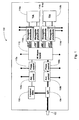
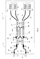
- FIG. 10 a schematic diagram of an exemplary QPSK chip is shown generally at 10.
- the chip substrate 12 may be constructed from InP. However, it is to be understood that the chip substrate 12 may be also be constructed from any semiconductor materials that are suitable for providing integration of optical waveguides, optical couplers, optical phase control and high speed detection within a compact device (e.g., InGaAs, InGaAsP).
- a compact device e.g., InGaAs, InGaAsP.
- the hybrid-90 is implemented on the chip using a 4x4 MMI coupler 14.
- the 4x4 MMI coupler 14 and other MMI couplers disclosed herein are of a standard design and are implemented within existing process design rules known in the art.
- the use of MMI couplers in hybrid-90 implementations is discussed, for example, in " Optical Multi-Mode Interference Devices Based on Self-Imaging: Principles and Applications” by Lucas B. Soldano and Erik C. M. Pennings, IEEE JOURNAL OF LIGHTWAVE TECHNOLOGY, VOL. 13, NO.
- the chip 10 includes input ports 16 and 18. More particularly, a QPSK encoded signal may be input to, and may be received by, at least one of input ports 16 and 18.
- the encoded data signal input to respective inputs ports 16 and 18 could represent a direct signal and a time-delayed signal.
- the encoded signal input to either of respective input ports 16 and 18 could represent a QPSK coded data-signal, and at the other input port, a reference signal from a LO (not illustrated) at a carrier frequency which is very close to that of the signal channel could be input.
- the chip 10 includes a plurality of waveguides 20 and 22 (i.e., input waveguides or optical channels) that couple respective ones of a signal input ports 16 and 18 to the 4X4 MMI coupler 14.
- a waveguide is a structure for guiding waves, in this case optical waves (signals).
- the optical signal may be passed through the respective waveguides 20 and 22 to the 4X4 MMI coupler 14.
- the waveguides 20 and 22 may be hard-walled on the chip 10 in order to support tight bends with low optical loss.
- a well-known ridge-guided design of waveguide can be fabricated by well-known methods of epitaxial growth and semiconductor etching to provide a set of semiconductor layers of controlled material composition and thickness so as to form a waveguide-core of one or more layers of higher refractive index with one or more cladding layers above and below of lower refractive index.
- the upper cladding, waveguide core and part of the lower cladding are etched away to define the width of the waveguide.
- the waveguides 20 and 22 are optically equivalent in birefringence and path length. Such optical equivalent waveguides are termed here "symmetrical.” The term symmetrical shall be understood to mean equivalent with respect to optical birefringence and optical path length, unless otherwise stated. Another way of describing the design for two equivalent waveguides would be a "matched pair" design. In applications where the chip 10 is used for any state-of-polarization, the waveguides 20 and 22 are designed to be identically or near-identically matched in length and width from the signal input up to the input of the 4x4 MMI coupler 14. This is to ensure that any birefringence in the waveguides is matched.
- the two waveguides 20 and 22 are coupled to separate specific inputs 24 of the 4x4 MMI coupler 14 for 90° phase mixer functionality. That is, the 4X4 MMI coupler 14 includes four inputs 24a-d, and two of the inputs 24 are respectively coupled to the waveguides 20 and 22 for receiving the input signal while the other two inputs 24 are unused.
- the waveguides 20 and 22 may be coupled to the inputs 24 in any of these specific possible arrangements (24a and 24b, 24a and 24c, 24c and 24d , and 24b and 24d).
- Phase and auxiliary controls may also be included along the waveguides 20 and 22.
- one or more phase electrodes 26 may be included along the waveguides 20 and 22 to enable adjustment of the relative optical phases of the signals.
- Resistive heaters on the top of the ridge-waveguide are used to provide a localised heating of the waveguide core which results in a modal refractive index change to adjust the optical phase.
- This refractive index change is substantially independent of polarization, and so this phase change does not introduce any substantial asymmetric birefringence when phase electrodes 26a and 26b are adjusted separately.
- a forward-bias current injected into the semiconductor core layers induces changes to the phase of the optical propagation which may be polarization dependent. This depends upon the extent to which the confinement of the optical mode to the waveguide core varies with the polarization of the optical mode.
- auxiliary electrodes 28 may be included along the waveguides 20 and 22 to control alignment and additional adjustment of the relative optical phases of the signals.
- auxiliary electrodes are connected to regions of the waveguide which are doped so as to form an electrical PIN diode structure, as is well known.
- the upper and lower cladding layer or layers are doped, or partly doped, with acceptors and donors to provide P or N-type conductivity, respectively, and the waveguide core layer is partly or wholly undoped, to form the intrinsic layer.
- the auxiliary electrode 28 can be deployed as forward-biased so as to inject carriers into the waveguide optical core, and so modify its optical properties; or reverse-biased so as to provide an electric field dependent modification of the optical properties of the waveguide optical core.
- the auxiliary electrode 28 introduces variable birefringence, which can be used to cancel out any other sources of birefringence which otherwise would lead to an undesirable polarization-dependent frequency shift (PDFS) in the performance of the DQPSK demodulator, as taught by C R Doerr, in a paper presented at ECOC-07.
- PDFS polarization-dependent frequency shift
- the auxiliary electrode 28 can be used either at relatively low reverse bias to adjust the phase and partially attenuate the optical signal in order to correct for any imbalance in coupling between the two inputs, (this correction also being polarization dependent); or, with an increased level of reverse-bias, to strongly attenuate the input light, and detect the resultant photocurrent so as to monitor the coupled optical power during set-up of the device.
- the waveguide PIN structure would be designed to have a semiconductor core layer or layers, which have a band-gap energy such that, under reverse-bias, the band-gap absorption edge has some degree of overlap with the photon energy of the optical signal.
- each of the input ports 16 and 18 of the chip 10 could additionally be an optional spot-size converter at each of the input ports 16 and 18 of the chip 10 for ease of optical alignment in fabrication.
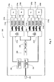
- the chip 10 includes high-speed waveguide photodiodes 30, 32, 34, and 36 (detectors) having sufficient bandwidth to detect the QPSK modulated signal at a given bit-rate.
- the waveguide photodiodes 30, 32, 34, and 36 include a combination of P-doped, intrinsic (undoped), and N-doped semiconductor layers, forming a PIN diode structure within a defined length of waveguide, in which the intrinsic layers include an absorbing layer of InGaAs (with a composition typically of In(0.53)Ga(0.47)As).
- An optical signal at the wavelength of operation of the receiver (for example 1550nm), is partly or wholly absorbed within this InGaAs layer along the length of the waveguide PIN diode, and generates electron and hole charge carriers in the semiconductor, which can be collected as a photocurrent at anode and cathode electrodes connected to the P-doped and N-doped layers, respectively, under application of a reverse-bias.
- the design of waveguide photodiodes is well known.
- On-chip decoupling capacitors may also optionally be included to mitigate the effects of electrical inductance from the external wirebonds which connect to and provide DC reverse bias to the cathodes of waveguide photodiodes 30, 32, 34, and 36.
- the decoupling capacitors can be constructed as either metal-insulator-metal (MIM) or metal-insulator-semiconductor (MIS) capacitors, as is well known to those skilled in the art.
- the waveguide photodiodes 30, 32, 34, and 36 may be constructed either as single-ended detectors respectively coupled to each of four outputs 46a-d of the 4X4 MMI coupler 14 with differential detection off-chip at the TIA (not illustrated), or as two pairs of balanced photodiodes for on-chip differential detection of the I-channel and Q-channel output pairs of the 4X4 MMI coupler 14.
- the single ended embodiment is illustrated, for example, in Figs. 3 and 4 .
- the balanced embodiment is discussed in more detail below with reference to Fig. 5 , for example.
- Waveguides 38, 40, 42, and 44 (i.e., output waveguides or optical channels) couple output ports 46 of the 4X4 MMI coupler 14 to the respective waveguide photodiodes 30, 32, 34, and 36.
- the optical signal may be passed through the respective waveguides 38, 44, 40, and 42 to the respective waveguide photodiodes 30, 32, 34, and 36.
- the waveguides 38, 40, 42, and 44 are arranged into two pairs. Waveguide pair 38 and 44 are respectively coupled at one end to output ports 46a and 46d (I-channel outputs having relative phase offsets 0° and 180°), and are respectively coupled at another end to photodiodes 30 and 32.
- Waveguide pair 40 and 42 are respectively coupled at one end to output ports 46b and 46c (Q-channel outputs having relative phase offsets 90° and 270°), and are respectively coupled at another end to photodiodes 34 and 36.
- the signals output from the 4x4 MMI coupler 14 may contain equal mixes of the two input signals 16 and 18, but with above-mentioned different relative phase offsets (i.e., 0°, 90°, 180°, and 270°).
- the waveguides 38, 40, 42, and 44 between the output of the 4X4 MMI coupler 14 and the photodiodes 30, 32, 34, and 36 are designed to be identical or near identical lengths. This is to ensure that, in operation, data skew between the I- and Q-channels is within an allowable upper limit (e.g., less than 5% of the data bit-period).
- an allowable upper limit e.g., less than 5% of the data bit-period.
- the waveguides 38, 40, 42, and 44 coupling the output of the 4X4 MMI coupler 14 to the respective photodiodes 30, 32, 34, and 36 are reordered as a precursor to balanced detection for the appropriate I- and Q-channels at the photodiodes.
- the waveguide 38 or 44 crosses over waveguides 40 and 42.
- the waveguides 38, 40, 42, and 44 may be reordered, for example, by using RF co-planar waveguide cross-overs (not illustrated). However, as described in detail below, waveguides 38, 40, 42, and 44 may be reordered by the use of one or more or a combination of dummy waveguide cross-overs or MMI cross-overs.
- the waveguides 38, 40, 42, and 44 coupled to the output ports 46 of the 4x4 MMI coupler 14 may be reordered by using optical waveguide cross-overs 48.
- the waveguide cross-over 48 is an intersection of two waveguides. As illustrated in Fig. 3 , waveguide cross-over 48a is present at the intersection of waveguide 44 and waveguide 42. Similarly, waveguide cross-over 48b is present at the intersection of waveguide 44 and waveguide 40. It is preferred that the cross-over 48 possesses a high angle of intersection to prevent cross-talk of the optical signal from one waveguide to the other. In one example, the angle of intersection is about 90°. In another, the angle of intersection is greater than 60°.
- the waveguide width may be in the range of about 1.0 to 2.5 microns.
- the optical signals which reach the photodiodes 30, 32, 34, and 36 are subject to optical losses in the waveguides 38, 40, 42, 44 and/or birefringence, and it is important to match (or balance) the optical losses for each of the waveguide outputs.
- Optical loss from waveguide cross-overs 48 can be a contribution to the optical loss in the waveguides.
- the losses may be balanced between waveguides 38 and 44 by including "dummy" cross-overs 50 in waveguide 38 to match the waveguide cross-overs 48 in waveguide 44.
- the dummy cross-over 50 may be fabricated with a "dummy" waveguide that intersects with the actual waveguide at the same or similar angle of intersection as cross-overs 48 to ensure the same loss.
- the dummy waveguide terminates at both ends and may have the same or similar ridge-width as the actual waveguide.
- waveguide 38 includes dummy waveguides 50a and 50b.
- dummy cross-overs 50 may be added to each of waveguides 40 and 42 to balance the average signal power and/or birefringence in the Q-channel with that in the I-channel.
- waveguide 40 includes dummy cross-over 50d
- waveguide 42 includes dummy cross-over 50c.
- the dummy cross-overs 50 in waveguides in 40 and 42 are optional.
- functional optical symmetry may be achieved among the respective waveguides 38, 40, 42, and 44.
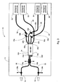
- the waveguides 38, 40, 42, and 44 coupled to the output ports 46 of the 4x4 MMI coupler 14 may be reordered by using double-length 2x2 MMI 3dB couplers 52, which function as optical cross-overs, as taught, for example, by L B Soldano (cited above).
- a standard 2x2 (paired-interference) MMI 3dB coupler is doubled in length, so as to have a length which is equal to the beat-length between the two lowest order modes within the MMI waveguide, then it acts as a cross-coupler, i.e. to transmit a signal to an output port that is a cross-port of the input port to which the signal was input.
- this 2x2 MMI cross-coupler will also be referred to as a double-length 2x2 MMI coupler and a double-length 2X2 MMI cross-over.
- waveguide 38 is directly coupled to photodiode 30.
- two double-length 2X2 MMI couplers 52 perform the function of crossing waveguide 44 over waveguides 40 and 42. Specifically, a first end of waveguide 44a is coupled to output port 46d of the 4X4 MMI coupler 14, and a second end of waveguide 44a is coupled to an input port of a double-length 2X2 MMI coupler 52a. A first end of waveguide 44b is coupled to the cross-port output port of double-length 2X2 MMI coupler 52a, and a second end of waveguide 44b is coupled to an input port of a double-length 2X2 MMI coupler 52b. A first end of waveguide 44c is coupled to the cross-port output port of MMI coupler 52b, and a second end of waveguide 44c is coupled to photodiode 32.
- Waveguide 42 is coupled to photodiode 36 via double-length 2X2 MMI coupler 52a. That is, a first end of waveguide 42a is coupled to output port 46c of the 4X4 MMI coupler 14, and a second end of waveguide 42a is coupled to a second input port of a double-length 2X2 MMI coupler 52a. A first end of waveguide 42b is coupled to the cross-port output port of double-length 2X2 MMI coupler 52a, and a second end of waveguide 42b is coupled to photodiode 36.
- Waveguide 40 is coupled to photodiode 34 via double-length 2X2 MMI coupler 52b. That is, a first end of waveguide 40a is coupled to output port 46b of the 4X4 MMI coupler 14, and a second end of waveguide 40a is coupled to a second input port of double-length 2X2 MMI coupler 52b. A first end of waveguide 40b is coupled to the cross-port output port of double-length 2X2 MMI coupler 52b, and a second end of waveguide 40b is coupled to photodiode 34.
- the advantage of using a double length 2X2 MMI coupler 52 as a cross-over within this optical hybrid chips is that the double-length 2X2 MMI coupler is laterally compact, keeping the waveguides close together.
- the dimensions of the double-length 2X2 MMI coupler are also chosen to give optimum transfer performance at the target wavelength and temperature of operation.
- the balancing of insertion loss and birefringence is achieved by the use of the double-length 2X2 MMI couplers 52, and the use of such double-length 2X2 MMI couplers 52 also achieves the functional optical symmetry among the respective waveguides 38, 40, 42, and 44.
- dummy double length 2X2 MMI cross-couplers may be introduced on the other waveguides in a manner similar to the dummy cross-overs 50 of Fig. 3 to balance any excess losses and birefringence on all waveguides, thereby further assisting to maintain said functional optical symmetry.
- two dummy double length 2X2 MMI cross-couplers may be introduced along waveguide 38.
- a dummy double length 2X2 MMI cross-coupler may be introduced along waveguide 40, and a dummy double length 2X2 MMI cross-coupler may be introduced along waveguide 42.
- the waveguide is input to an input port of the dummy double-length 2X2 MMI coupler, and output from a cross-port output port of the dummy double-length 2X2 MMI coupler.
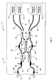
- Balanced (or differential) detection can be accomplished with two pairs of single-ended photodiodes on the chip (as shown in Figs. 3 and 4 ) with the outputs of each pair connected to differential input TIAs.
- balanced (or differential) detection can be accomplished directly on the chip 10 with two pairs of balanced photodiodes 31 and 35 on the chip 10.
- photodiodes 30 and 32 are operated as pair 31 and photodiodes 34 and 36 are operated as pair 35
- the difference in photocurrent between 30 and 32 I 30 -I 32
- the difference in photocurrent between 34 and 36 I 34 -I 36
- a balanced photodiode pair 31 and 35 is constructed by connecting the anode of one photodiode to the cathode of the other, and monitoring the net signal of the two photodiodes at this point, the two photodiodes having matched responsivity and electrical bandwidth.
- electrical isolation is provided between the P-doped semiconductor regions (which connect to the individual anodes) of the two photodiodes and between the N-doped semiconductor layers (which connect to the individual cathodes) of the two photodiodes.
- isolation between the P-doped semiconductor regions of the two photodiodes is provided, with N-doped regions connected (common cathode); or isolation between the N-doped semiconductor regions of the two photodiodes is provided, with P-doped regions connected (common anode).
- both the P-doped and N-doped interconnecting layers can be electrically isolated between the photodiodes.
- the hybrid-90 may be implemented as a network of symmetric 2X2 MMI couplers 54, 56, 58, 60 on the QPSK chip instead of as the above-described 4X4 MMI coupler 14.
- Figs. 6-8 illustrate examples of a QPSK chip 10 including such network, with single-ended waveguide photodiodes 30, 32, 34, and 36 on each of the four outputs of the network.
- the chip 10 is designed so that waveguides 20 and 22 respectively couple the input ports 16 and 18 of the chip 10 to the 2X2MMI couplers 54 and 56.
- the two waveguides 20 and 22 are coupled to separate specific inputs of the respective 2X2 MMI couplers 54 and 56. That is, the 2X2 MMI couplers 54 and 56 each include two inputs, and one of the inputs of each 2X2 MMI coupler 54 and 56 is respectively coupled to one of the waveguides 20 and 22 while the other input is unused.
- Waveguides 62, 64, 66, and 68 respectively couple the 2X2 MMI couplers 54 and 56 to 2X2 MMI couplers 58 and 60.
- the four separate optical paths which interconnect the MMIs 54 and 56 to the MMIs 58 and 60 are matched in length.
- This network of MMIs and waveguides also includes an optical waveguide cross-over 48 between I- and Q-channels. As illustrated in Fig. 6 , the optical waveguide cross-over may be implemented as a simple waveguide cross-over 48 similar to the cross-overs 48 discussed in relation to Fig. 3 . In this example, dummy cross-overs are disposed along the path of each of waveguides 62 and 68.
- the optical waveguide cross-over may be implemented as a double-length 2X2 MMI coupler 70 which functions as a cross-over similar to the double-length 2X2 MMI couplers 52 discussed in relation to Fig. 4 .
- dummy double-length 2x2 MMI couplers 67a and 67b may also be introduced along waveguides 62 and 68 to ensure that any excess losses are matched on all waveguides, thereby maintaining said functional optical symmetry.
- Network phase electrodes 26c and 26d may be introduced along waveguides 62 and 68 in addition to the input phase electrodes 26a and 26b and auxiliary electrodes 28. These network phase electrodes 26c and 26d may be adjusted to introduce a 90° phase change between the I- and Q-channels.
- This network of 2X2 MMIs couplers may be modified to include a 1X2 (symmetric interference) MMI coupler that performs the above-mentioned 90° phase change function.
- Fig. 9 illustrates the use of a 1X2 MMI coupler 72 in place of 2X2 MMI coupler 54.
- the 1x2 MMI coupler 72 acts to introduce the 90° phase change between the I- and Q-channels in the network.
- the network phase electrodes 26c and 26d may still be included for making small corrections to the phase (as opposed to the full 90° phase change).
- the asymmetry in the lengths of the 2x2 MMI coupler 56 and the 1x2 MMI coupler 72 may be corrected by adjusting the length of waveguide 20 so as to give an optical path length which is equal to that of the input waveguide to the 2x2 MMI coupler 56.
- the asymmetry in the network may affect the balance of optical power in the output waveguides 38, 40, 42, 44.
- the insertion loss of 1x2 MMI coupler 72 may differ from that of 2x2 MMI coupler 56.
- one or both of the dummy waveguides 50a and 50b may not be required and are therefore optional.
- the 2x2MMI coupler 56 may be designed such that it has a deliberate imbalance in its output power into waveguides 66 and 68 to offset such asymmetry.
- the optical waveguide cross-over 48 (and dummy cross-overs 50) may instead be implemented as a double-length 2X2 MMI coupler 70 (and dummy double-length 2X2 MMI couplers 67), similar to the example of Figs. 7 and 8 .
- ⁇ 2 ⁇ ⁇ n Z / ⁇ .
- Still another conventional approach of introducing a 90° phase offset includes adding a phase-control electrode to one or more of the network waveguides.
- the setting of this phase-control may need to be fixed over wavelength and temperature, which is difficult to accomplish.
- ⁇ n may have a wavelength dependence, due to differences in the temperature dependence of the optical properties of the materials used to construct the waveguide.
- the phase-control needs to be adapted according to the operating temperature T.
- n(T) will not in general have a purely linear dependence on temperature, and more importantly the local heating achieved in the waveguide, ⁇ T, depends upon both the dissipated power in the resistor and the thermal conductivities of the materials which comprise the waveguide. Any temperature dependence of these properties will result in a different heating effect, ⁇ T, as the operating temperature is changed.
- Other methods include modifying the refractive index of the waveguide core through either the application of a forward-bias (so as to introduce a controlled density of carriers into the waveguide core) or a reverse-bias (so as to introduce a controlled electric field into the waveguide core). This method has a phase-dependence which is dependent upon the wavelength of operation.
- the phase-relationships of the input and output ports of the 1x2 MMI coupler 72 and 2x2 MMI coupler 56 are fixed by their design. Also, there is a range of operation over which the MMI design is tolerant to changes in wavelength and temperature. By utilising the difference in the intrinsic input/output phase-relationship of 1x2 and 2x2 MMI couplers, rather than modifying the phase within the waveguide network, improved stability of performance over a wider range of wavelength and temperature operating conditions is achieved. Furthermore, the network of Fig. 9 has the advantage of minimizing the impact of any polarization dependence associated with either or both of the network phase controls 26c and 26d.
- the above-discussed network of 2X2 MMI couplers 54, 56, 58, and 60 may also be modified so that 2X2 MMI couplers 54 and 56 are replaced by 1X2 MMI couplers 69 and 71.
- Such modified network can provide an advantage of improved split-ratio process tolerance.
- Figures 11 and 12 illustrate examples of QPSK chips 10 based upon a network of 2x2 MMIs 54, 56, 58, and 60 acting as 3dB couplers in a manner similar to that discussed in relation to Figs. 7 and 8 , with dummy waveguide cross-overs, and with two pairs of balanced waveguide photodiodes 31 and 35.
- Fig. 13 illustrates an example of the QPSK chip 10, wherein the configuration of the chip is designed to meet the requirement to couple to two separate TIAs (not illustrated).
- Waveguides 38, 40, 42, and 44 include cross-overs similar to those discussed in relation to Fig. 3 .
- Photodiode pairs 30 and 32; 34 and 36 are located on two adjacent sides of the chip 10 rather than on the same side. Of course, other configurations are possible (e.g., all on the same side, on opposite sides of the chip, etc.).
- Fig. 14 illustrates an example of a chip 10 with integrated balanced waveguide photodiodes 31 and 35 for use in a PDM-QPSK demodulator.
- the input signal is in QPSK format for two different orthogonal polarization states.
- the input signal is split into the two separate polarization components off-chip, and one of these is rotated into the common single state of polarization used on the chip.
- the chip therefore has two optical signal input ports 16 and 18, and also an input port 17 for a LO signal which provides the reference phase for decoding the phase-shift data encoded on the two QPSK signals.
- the input port 17 is coupled to a 1X2 MMI coupler 13, which in turn is coupled to 4X4 MMI couplers 14a and 14b and with provision of dummy waveguide cross-overs.
- a 1X2 MMI coupler 13 which in turn is coupled to 4X4 MMI couplers 14a and 14b and with provision of dummy waveguide cross-overs.
- the chip illustrated in Fig. 13 could be alternatively designed using any of the foregoing chip designs, and/or with single-ended photodiodes 30, 32, 34, and 36.
- the optical delay may be constructed as an optical block which splits the optical input signal into two signals and delaying one of the two split signals by one bit period or by a period plus or minus a fraction of a bit period.
- the delayed and undelayed output signals from the optical delay may be respectively coupled to the inputs of the QPSK chip 10 of the present invention.
- this delay can be variable in length. The optical delay can be adjusted by adjustment of the optical block.
- Performing optical delay off-chip overcomes the disadvantages associated with having a limited amount of control of the on-chip optical delay, while providing for relatively easy customization of the delay period to suit individual requirements.
- the same QPSK chip can be used with any one of a plurality of off-chip optical delays, and vice versa.
- Figure 15 illustrates of the principles of operation of the optical delay system 74.
- An input light beam 76 is incident on an optical block 78 at S1 and is refracted to point S2 where it is split. Specifically, about 50% of the beam 76 is transmitted and about 50% of the beam 76 is reflected.
- the transmitted beam 76 continues along path 1 through one or more lenses 80, 82 to an input port on the chip (not illustrated).
- the beam 76 reflected at S2 is further reflected at S3 and leaves the block at S4 from where it continues along path 2 through one or more lenses 84 and 86 to a separate input port on the chip.
- the lenses direct the beams along paths 1 and 2 into the respective waveguides on the chip.
- the optical path difference (which determines the optical delay) and separation of the two beams will be dependent upon the thickness of the block 78 and the angle of incidence to the input light beam 76.
- the delay and separation will also be dependent upon the refractive index of the optical block 78.
- the reflective properties of the facets of the block are determined by applying anti-reflective (AR) coatings at S1 and S4, applying a 50% reflective coating at S2 and a 100% reflective coating at S3.
- AR anti-reflective
- the optical block system may further include a tunable delay 88.
- the tunable delay 88 may be made of a material such as silicon, which when heated in a controlled way, can trim the optical path over a fraction of a bit period.
- Fig. 16 illustrates an example of the optical delay system which incorporates the thermally tunable delay 88 in one of the output optical paths between the optical block 78 and the chip.
- Fig. 17 illustrates an example of the optical delay system which incorporates the thermally tunable delay 88 on the optical block 78 (e.g., at S4) rather than, as in Figure 16 , to the lenses.
- Figure 18 illustrates an optical element 90 that can be used when polarization diversity is desired. It consists of two polarization beam splitters 92(PBS) and a half-wave plate 94, the dimensions of the PBS cube are used to effect beam separation.
- the device takes a beam 77 of input light (including TE and TM polarizations, splits it into TE and TM polarizations, and convert the TM beam to TE so that the two TE beams are applied to the optical receiver chip.
- two TM beams may similarly be produced and applied to the optical receiver chip.
Landscapes
- Engineering & Computer Science (AREA)
- Computer Networks & Wireless Communication (AREA)
- Signal Processing (AREA)
- Physics & Mathematics (AREA)
- Electromagnetism (AREA)
- Optical Integrated Circuits (AREA)
- Optical Communication System (AREA)
Claims (8)
- Puce de modulation par déplacement de phase quadrivalente (10), modulation QPSK, destinée à démoduler un signal optique, comprenant :une entrée (16, 18) pour recevoir un signal modulé QPSK ;un mélangeur hybride optique pour recevoir le signal modulé QPSK et mélanger le signal modulé QPSK dans une pluralité de signaux de sortie ;une pluralité de photodiodes (30, 32, 24, 26), détectant chacune un signal correspondant parmi la pluralité de signaux de sortie ; etune pluralité de guides d'onde de sortie (38, 40, 42, 44), couplant chacun une photodiode parmi la pluralité de photodiodes à une sortie respective du mélangeur hybride optique correspondant à un signal de la pluralité de signaux de sortie ;caractérisé en ce que le mélangeur hybride optique comprend un réseau asymétrique de coupleurs à interférence multimode, MMI, qui comprend un coupleur MMI 1X2 (72) et un premier coupleur MMI 2X2 (56).
- Puce de modulation QPSK selon la revendication 1, dans laquelle le coupleur MMI 1X2 (72) et le coupleur MMI 2X2 (56) communiquent une différence de phase de 90° au signal modulé QPSK.
- Puce QPSK selon la revendication 1 ou 2, dans laquelle
le coupleur MMI 1X2 (72) comprend une pluralité de sorties (62, 64) ;
le premier coupleur MMI 2X2 (56) comprend une pluralité de sorties ; et
une pluralité de guides d'onde intermédiaires (62, 64, 66, 68) couplent les sorties respectives du coupleur MMI 1X2 et du premier coupleur MMI 2X2 à un coupleur parmi un deuxième coupleur MMI 2X2 (58) et un troisième coupleur MMI 2X2 (60). - Puce de modulation QPSK selon la revendication 3, comprenant une jonction (48) entre au moins deux guides de la pluralité de guides d'onde intermédiaires.
- Puce de modulation QPSK selon la revendication 4, dans laquelle le mélangeur hybride optique comprend au moins une jonction de guide d'onde fictif (50a, 50b) incluse le long d'un guide d'onde de la pluralité de guides d'onde intermédiaires (62, 68) en vue de compenser au moins l'un parmi un affaiblissement d'insertion et une biréfringence entre la pluralité de guides d'onde intermédiaires, et la première jonction de guide d'onde fictive compense un déséquilibre occasionné par la jonction entre au moins deux guides de la pluralité de guides d'onde intermédiaires.
- Puce de modulation QPSK selon la revendication 4, dans laquelle le mélangeur hybride optique inclut un coupleur MMI double longueur (70) inclus le long d' au moins deux guides de la pluralité de guides d'onde intermédiaires en vue de joindre les au moins deux guides de la pluralité de guides d'onde intermédiaires et de compenser au moins l'un parmi un affaiblissement d'insertion et une biréfringence entre la pluralité de guides d'onde intermédiaires.
- Puce de modulation QPSK selon l'une quelconque des revendications précédentes, dans laquelle le premier coupleur MMI 2X2 (56) est conçu de manière à présenter un déséquilibre volontaire dans sa puissance de sortie.
- Puce de modulation QPSK selon l'une quelconque des revendications précédentes, dans laquelle l'entrée est couplée à une unité de retardement hors puce (74) qui divise et retarde le signal modulé QPSK.
Applications Claiming Priority (2)
| Application Number | Priority Date | Filing Date | Title |
|---|---|---|---|
| US15299209P | 2009-02-17 | 2009-02-17 | |
| EP10710425.9A EP2399374B8 (fr) | 2009-02-17 | 2010-02-17 | Puces optiques et dispositifs pour des communications optiques |
Related Parent Applications (2)
| Application Number | Title | Priority Date | Filing Date |
|---|---|---|---|
| EP10710425.9 Division | 2010-02-17 | ||
| EP10710425.9A Division EP2399374B8 (fr) | 2009-02-17 | 2010-02-17 | Puces optiques et dispositifs pour des communications optiques |
Publications (3)
| Publication Number | Publication Date |
|---|---|
| EP2624513A2 EP2624513A2 (fr) | 2013-08-07 |
| EP2624513A3 EP2624513A3 (fr) | 2013-10-23 |
| EP2624513B1 true EP2624513B1 (fr) | 2014-06-25 |
Family
ID=42634274
Family Applications (2)
| Application Number | Title | Priority Date | Filing Date |
|---|---|---|---|
| EP13165776.9A Active EP2624513B1 (fr) | 2009-02-17 | 2010-02-17 | Puces optiques et dispositifs pour communications optiques |
| EP10710425.9A Active EP2399374B8 (fr) | 2009-02-17 | 2010-02-17 | Puces optiques et dispositifs pour des communications optiques |
Family Applications After (1)
| Application Number | Title | Priority Date | Filing Date |
|---|---|---|---|
| EP10710425.9A Active EP2399374B8 (fr) | 2009-02-17 | 2010-02-17 | Puces optiques et dispositifs pour des communications optiques |
Country Status (5)
| Country | Link |
|---|---|
| US (1) | US9020367B2 (fr) |
| EP (2) | EP2624513B1 (fr) |
| JP (1) | JP2012518202A (fr) |
| CN (1) | CN102396196B (fr) |
| WO (1) | WO2010095018A2 (fr) |
Families Citing this family (65)
| Publication number | Priority date | Publication date | Assignee | Title |
|---|---|---|---|---|
| US8401399B2 (en) * | 2009-05-28 | 2013-03-19 | Freedom Photonics, Llc. | Chip-based advanced modulation format transmitter |
| US9344196B1 (en) | 2009-05-28 | 2016-05-17 | Freedom Photonics, Llc. | Integrated interferometric optical transmitter |
| KR20110030136A (ko) * | 2009-09-17 | 2011-03-23 | 한국전자통신연구원 | 편광 분리기, 광학 하이브리드 그리고 그것들을 포함하는 광 수신기 |
| EP2410309B1 (fr) * | 2010-07-20 | 2017-06-21 | U2t Photonics Ag | Procédé et système de caractérisation d'un dispositif optique |
| EP2413170B1 (fr) * | 2010-07-28 | 2013-02-13 | u2t Photonics AG | Dispositif optique |
| GB2485202B (en) | 2010-11-05 | 2017-08-30 | Oclaro Tech Ltd | Demodulator and optical arrangement thereof |
| JPWO2012086846A1 (ja) * | 2010-12-21 | 2014-06-05 | 日本電気株式会社 | 光導波路デバイス及び光導波路デバイスの製造方法 |
| KR20120071120A (ko) * | 2010-12-22 | 2012-07-02 | 한국전자통신연구원 | 평판형 도파로 기반 반사형 광 지연 간섭계 장치 |
| US8750651B2 (en) * | 2010-12-22 | 2014-06-10 | Alcatel Lucent | Planar polarization rotator |
| JP5640829B2 (ja) * | 2011-03-09 | 2014-12-17 | 富士通株式会社 | 光ハイブリッド回路、光受信機及び光受信方法 |
| JP2012198292A (ja) * | 2011-03-18 | 2012-10-18 | Fujitsu Ltd | 光ハイブリッド回路及び光受信機 |
| US10009115B2 (en) * | 2011-05-02 | 2018-06-26 | Massachusetts Institute Of Technology | Optical receiver configurable to accommodate a variety of modulation formats |
| WO2013015391A1 (fr) * | 2011-07-25 | 2013-01-31 | 日本電気株式会社 | Photorécepteur, dispositif de photoréception l'utilisant et procédé de photoréception |
| JP5866911B2 (ja) * | 2011-09-16 | 2016-02-24 | 住友電気工業株式会社 | 多チャネル光導波路型受光デバイス |
| US9379821B2 (en) * | 2011-09-26 | 2016-06-28 | The Provost, Fellows, Foundation Scholars, And The Other Members Of Board, Of The College Of The Holy And Undivided Trinity Of Queen Elizabeth Near Dublin | Optical receiver |
| CN102427439B (zh) * | 2011-11-28 | 2015-02-18 | 武汉光迅科技股份有限公司 | 一种应用dqpsk解调器消除偏振相关频率漂移的方法及其产品 |
| CN104160641B (zh) * | 2012-03-06 | 2016-09-14 | 日本电气株式会社 | 平面光波回路和光学接收器 |
| US9130692B2 (en) * | 2012-04-23 | 2015-09-08 | Coriant Operations, Inc. | Reconfigurable optical add/drop multiplexer network element for C-band and L-band optical signals |
| JP5900174B2 (ja) * | 2012-06-08 | 2016-04-06 | 住友電気工業株式会社 | コヒーレントミキサ、コヒーレントミキサを作製する方法 |
| JP5839586B2 (ja) * | 2012-08-30 | 2016-01-06 | 日本電信電話株式会社 | 光信号処理装置 |
| JP5920128B2 (ja) * | 2012-09-07 | 2016-05-18 | 住友電気工業株式会社 | 光導波路型受光素子の製造方法および光導波路型受光素子 |
| US9477134B2 (en) * | 2012-12-28 | 2016-10-25 | Futurewei Technologies, Inc. | Hybrid integration using folded Mach-Zehnder modulator array block |
| DE102013204731B4 (de) * | 2013-03-18 | 2017-11-16 | Fraunhofer-Gesellschaft zur Förderung der angewandten Forschung e.V. | Analog-Digital-Konverter und Verfahren zum Erzeugen eines digitalen Datenstromes |
| JP2015068854A (ja) * | 2013-09-26 | 2015-04-13 | 住友電気工業株式会社 | 光学素子および波長モニタ |
| JP6167847B2 (ja) * | 2013-10-25 | 2017-07-26 | 富士通オプティカルコンポーネンツ株式会社 | 光受信装置、光送受信モジュール及び光送受信装置 |
| JP6364830B2 (ja) * | 2014-03-11 | 2018-08-01 | 住友電気工業株式会社 | 半導体光集積素子 |
| JP6346803B2 (ja) | 2014-06-23 | 2018-06-20 | 株式会社フジクラ | 光受信回路およびその調整方法 |
| CN106464384B (zh) * | 2014-09-17 | 2019-09-13 | 华为技术有限公司 | 一种光信号调制装置和系统 |
| JP2016072464A (ja) * | 2014-09-30 | 2016-05-09 | 住友電気工業株式会社 | 光伝送装置 |
| JP6428146B2 (ja) * | 2014-10-22 | 2018-11-28 | 日本電気株式会社 | 光導波路デバイス及びその製造方法 |
| CN104320199B (zh) * | 2014-10-27 | 2017-05-03 | 中国科学院半导体研究所 | InP基单片集成少模光通信接收器芯片 |
| US10110318B2 (en) * | 2015-02-19 | 2018-10-23 | Elenion Technologies, Llc | Optical delay lines for electrical skew compensation |
| CN107430312A (zh) * | 2015-03-09 | 2017-12-01 | 住友电工光电子器件创新株式会社 | 相干接收器 |
| WO2016149826A1 (fr) * | 2015-03-23 | 2016-09-29 | Artic Photonics Inc. | Récepteur cohérent intégré et comportant un agencement géométrique pour améliorer l'efficacité d'un dispositif |
| KR102180382B1 (ko) * | 2015-05-13 | 2020-11-19 | 한국전자통신연구원 | 수신용 광 모듈 |
| WO2016194349A1 (fr) * | 2015-05-29 | 2016-12-08 | 日本電信電話株式会社 | Circuit mélangeur optique cohérent |
| JP2017032629A (ja) | 2015-07-29 | 2017-02-09 | 住友電気工業株式会社 | 光モジュール |
| JP6500750B2 (ja) | 2015-11-05 | 2019-04-17 | 住友電気工業株式会社 | 半導体光素子、半導体組立体 |
| CN105515654B (zh) * | 2015-11-30 | 2018-06-26 | 武汉光迅科技股份有限公司 | 一种并联mzi结构开关电压和消光比的测量方法 |
| EP3437213B1 (fr) | 2016-03-29 | 2022-08-24 | Nokia Technologies Oy | Mesure de l'état de bell |
| CN106301554B (zh) * | 2016-08-31 | 2019-01-22 | 武汉光迅科技股份有限公司 | 一种并联mzi电光调制器工作点电压的调试方法及调试装置 |
| US10514516B2 (en) * | 2017-03-03 | 2019-12-24 | Sumitomo Electric Device Innovations, Inc. | Semiconductor optical device monolithically integrating optical waveguides with photodiodes having a shared bias pad and apparatus implementing the same |
| US10320152B2 (en) | 2017-03-28 | 2019-06-11 | Freedom Photonics Llc | Tunable laser |
| US10551714B2 (en) * | 2017-05-17 | 2020-02-04 | Finisar Sweden Ab | Optical device |
| JP6476264B1 (ja) * | 2017-11-07 | 2019-02-27 | 沖電気工業株式会社 | 光ハイブリッド回路 |
| JP6919557B2 (ja) * | 2017-12-26 | 2021-08-18 | 住友電気工業株式会社 | 光90度ハイブリッド集積回路 |
| GB201722292D0 (en) * | 2017-12-29 | 2018-02-14 | Oclaro Tech Ltd | Negative bias to improve phase noise |
| GB201722293D0 (en) | 2017-12-29 | 2018-02-14 | Oclaro Tech Ltd | Balancing losses in semiconductor optical waveguides |
| FR3077887B1 (fr) * | 2018-02-13 | 2021-07-23 | St Microelectronics Crolles 2 Sas | Puce optoelectronique et procede de test de circuits photoniques d'une telle puce |
| FR3077888B1 (fr) | 2018-02-13 | 2020-02-28 | Stmicroelectronics (Crolles 2) Sas | Puce optoelectronique et procede de test de circuits photoniques d'une telle puce |
| JP7037958B2 (ja) * | 2018-02-27 | 2022-03-17 | 住友電気工業株式会社 | 半導体光集積デバイス |
| JP7302946B2 (ja) * | 2018-03-13 | 2023-07-04 | 富士通オプティカルコンポーネンツ株式会社 | 光デバイス、およびこれを用いた光通信モジュール |
| CN112236688B (zh) * | 2018-06-12 | 2024-03-22 | 三菱电机株式会社 | 光测距装置以及加工装置 |
| US10731383B2 (en) * | 2018-08-01 | 2020-08-04 | Macom Technology Solutions Holdings, Inc. | Symmetric coherent optical mixer |
| JP6704436B2 (ja) * | 2018-08-15 | 2020-06-03 | 沖電気工業株式会社 | 光ハイブリッド回路 |
| JP2020030333A (ja) | 2018-08-23 | 2020-02-27 | 住友電工デバイス・イノベーション株式会社 | 光90°ハイブリッド素子 |
| FR3090249B1 (fr) * | 2018-12-18 | 2020-12-18 | Thales Sa | Dispositif et système de recombinaison cohérente de faisceaux optiques multi-longueur d’onde |
| JP7181462B2 (ja) * | 2019-01-17 | 2022-12-01 | 日本電信電話株式会社 | 光検出器 |
| CN109981179A (zh) * | 2019-03-09 | 2019-07-05 | 北京爱杰光电科技有限公司 | 一种无需90°移相器的单片集成qpsk发射芯片 |
| CN114365033A (zh) * | 2019-09-13 | 2022-04-15 | 日本电信电话株式会社 | Iq光调制器 |
| US10767974B1 (en) * | 2019-12-10 | 2020-09-08 | Rockwell Collins, Inc. | Wide range optical wavelength fast detection for narrowband signal |
| US11333831B2 (en) * | 2020-09-21 | 2022-05-17 | Ii-Vi Delaware, Inc. | Optical couplers and hybrids |
| US11294119B1 (en) | 2020-11-19 | 2022-04-05 | Cisco Technology, Inc. | Multimode-interference waveguide crossings |
| US20220244464A1 (en) * | 2021-02-02 | 2022-08-04 | Macom Technology Solutions Holdings, Inc. | Multimode splitter for narrowing input width photodetector connections |
| EP4266016A1 (fr) * | 2022-04-22 | 2023-10-25 | Rockwell Collins, Inc. | Auto-étalonnage multipoint pour interrogateur de capteur optique à large bande |
Family Cites Families (22)
| Publication number | Priority date | Publication date | Assignee | Title |
|---|---|---|---|---|
| US3988705A (en) * | 1975-11-20 | 1976-10-26 | Rockwell International Corporation | Balanced four-way power divider employing 3db, 90° couplers |
| JPS63234228A (ja) * | 1987-03-24 | 1988-09-29 | Oki Electric Ind Co Ltd | 光マトリクススイツチ |
| DE3871412D1 (de) * | 1987-03-10 | 1992-07-02 | Oki Electric Ind Co Ltd | Optische schaltmatrix. |
| US4858958A (en) * | 1988-03-14 | 1989-08-22 | Harbeke Gerold J | Slip-joint coupling |
| US6259834B1 (en) * | 1999-07-29 | 2001-07-10 | Lynx Photonic Networks Inc. | Dense tree optical switch network |
| JP2001147452A (ja) * | 1999-11-18 | 2001-05-29 | Oki Electric Ind Co Ltd | 光素子 |
| EP1329047A1 (fr) * | 2000-09-26 | 2003-07-23 | Celight, Inc. | Systeme et procede destines a la communication optique multiplexee par repartition de code |
| JP2003060575A (ja) * | 2001-08-20 | 2003-02-28 | Japan Telecom Co Ltd | 光通信システム及びその受信側制御方法 |
| US7327913B2 (en) * | 2001-09-26 | 2008-02-05 | Celight, Inc. | Coherent optical detector and coherent communication system and method |
| WO2003036834A1 (fr) * | 2001-09-26 | 2003-05-01 | Celight, Inc. | Procede et systeme de communications optiques par fibre a multiplexage temporel avec detection coherente |
| JP3878012B2 (ja) * | 2001-12-21 | 2007-02-07 | 日本電信電話株式会社 | 光導波回路 |
| GB2385144B (en) | 2002-01-23 | 2006-02-08 | Marconi Optical Components Ltd | Optical signal demodulators |
| JP2004051128A (ja) | 2002-07-17 | 2004-02-19 | Nippon Giken Kogyo Kk | 家庭用ポリエチレン袋の店頭販売用包装袋 |
| JP4058402B2 (ja) * | 2002-11-19 | 2008-03-12 | 日本電信電話株式会社 | 光導波回路 |
| US6909835B2 (en) * | 2003-07-15 | 2005-06-21 | Lucent Technologies Inc. | Configurations for waveguide crossings |
| US7058259B2 (en) * | 2003-08-14 | 2006-06-06 | Lucent Technologies Inc. | Optical device having a waveguide lens with multimode interference |
| US7343104B2 (en) * | 2004-06-23 | 2008-03-11 | Lucent Technologies Inc. | Apparatus and method for receiving a quadrature differential phase shift key modulated optical pulsetrain |
| US7650084B2 (en) * | 2005-09-27 | 2010-01-19 | Alcatel-Lucent Usa Inc. | Optical heterodyne receiver and method of extracting data from a phase-modulated input optical signal |
| JP5055947B2 (ja) * | 2006-10-20 | 2012-10-24 | 富士通オプティカルコンポーネンツ株式会社 | 光変調器および送信装置 |
| JP4365416B2 (ja) | 2007-01-17 | 2009-11-18 | 日本電信電話株式会社 | 光多値変調信号用光遅延検波回路 |
| JP4918400B2 (ja) | 2007-04-27 | 2012-04-18 | 富士通株式会社 | 光信号受信装置 |
| JP5287527B2 (ja) * | 2008-12-26 | 2013-09-11 | 富士通株式会社 | 光ハイブリッド回路、光受信機及び光受信方法 |
-
2010
- 2010-02-17 US US13/202,088 patent/US9020367B2/en active Active
- 2010-02-17 WO PCT/IB2010/000303 patent/WO2010095018A2/fr active Application Filing
- 2010-02-17 EP EP13165776.9A patent/EP2624513B1/fr active Active
- 2010-02-17 JP JP2011550663A patent/JP2012518202A/ja active Pending
- 2010-02-17 CN CN201080016962.6A patent/CN102396196B/zh active Active
- 2010-02-17 EP EP10710425.9A patent/EP2399374B8/fr active Active
Also Published As
| Publication number | Publication date |
|---|---|
| EP2624513A2 (fr) | 2013-08-07 |
| US20120106984A1 (en) | 2012-05-03 |
| JP2012518202A (ja) | 2012-08-09 |
| CN102396196B (zh) | 2014-11-26 |
| CN102396196A (zh) | 2012-03-28 |
| US9020367B2 (en) | 2015-04-28 |
| EP2624513A3 (fr) | 2013-10-23 |
| EP2399374B8 (fr) | 2013-06-19 |
| EP2399374B1 (fr) | 2013-05-01 |
| WO2010095018A2 (fr) | 2010-08-26 |
| EP2399374A2 (fr) | 2011-12-28 |
| WO2010095018A3 (fr) | 2011-07-07 |
Similar Documents
| Publication | Publication Date | Title |
|---|---|---|
| EP2624513B1 (fr) | Puces optiques et dispositifs pour communications optiques | |
| US11811433B2 (en) | Integrated coherent optical transceiver | |
| US8526102B2 (en) | PLC-type demodulator and optical transmission system | |
| Jeong et al. | Novel Optical 90$^{\circ} $ Hybrid Consisting of a Paired Interference Based 2$\,\times\, $4 MMI Coupler, a Phase Shifter and a 2$\,\times\, $2 MMI Coupler | |
| CN107925484B (zh) | 一种单片集成相干光接收器芯片 | |
| Doerr et al. | Monolithic PDM-DQPSK receiver in silicon | |
| US8299417B2 (en) | Variable optical attentuator (VOA) having an absorber for receiving residual light outputfrom the VOA | |
| US8213802B2 (en) | Receiver on a photonic IC | |
| US20160127070A1 (en) | Integrated two-channel spectral combiner and wavelength locker in silicon photonics | |
| WO2010021669A2 (fr) | Détecteurs optiques cohérents monolithiques | |
| Murata et al. | 100-Gbit/s PDM-QPSK coherent receiver with wide dynamic range and excellent common-mode rejection ratio | |
| Ma et al. | Symmetrical polarization splitter/rotator design and application in a polarization insensitive WDM receiver | |
| JP5640829B2 (ja) | 光ハイブリッド回路、光受信機及び光受信方法 | |
| CN115917996A (zh) | 芯片上的光相干接收器 | |
| US9379821B2 (en) | Optical receiver | |
| US20090074426A1 (en) | Monolithic dqpsk receiver | |
| Okimoto et al. | InP-based PIC integrated with butt-joint coupled waveguide pin PDs for 100GBaud coherent networks | |
| Oguma et al. | Single MZI-based 1x4 DQPSK demodulator | |
| Zhou et al. | Silicon photonics for advanced optical communication systems | |
| Takechi et al. | Compact optical receivers for coherent optical communication | |
| GOTOH et al. | Coherent Receiver for L-band | |
| Nasu et al. | Polarization insensitive MZI-based DQPSK demodulator with asymmetric half-wave plate configuration | |
| Hashimoto | Integrated optical receivers using planar lightwave circuit technology | |
| Hideki et al. | InP-Based Monolithically Integrated Photonics for 100/200 Gb/s Coherent Transceivers | |
| Skahan et al. | Monolithically integrated dual-channel coherent receiver with widely tunable local oscillator for 100 Gbps dual-polarization quadrature phase shift keying applications |
Legal Events
| Date | Code | Title | Description |
|---|---|---|---|
| PUAI | Public reference made under article 153(3) epc to a published international application that has entered the european phase |
Free format text: ORIGINAL CODE: 0009012 |
|
| AC | Divisional application: reference to earlier application |
Ref document number: 2399374 Country of ref document: EP Kind code of ref document: P |
|
| AK | Designated contracting states |
Kind code of ref document: A2 Designated state(s): AT BE BG CH CY CZ DE DK EE ES FI FR GB GR HR HU IE IS IT LI LT LU LV MC MK MT NL NO PL PT RO SE SI SK SM TR |
|
| PUAL | Search report despatched |
Free format text: ORIGINAL CODE: 0009013 |
|
| AK | Designated contracting states |
Kind code of ref document: A3 Designated state(s): AT BE BG CH CY CZ DE DK EE ES FI FR GB GR HR HU IE IS IT LI LT LU LV MC MK MT NL NO PL PT RO SE SI SK SM TR |
|
| RIC1 | Information provided on ipc code assigned before grant |
Ipc: H04J 14/06 20060101ALI20130918BHEP Ipc: H04L 27/22 20060101AFI20130918BHEP Ipc: G02B 6/28 20060101ALI20130918BHEP Ipc: H04B 10/60 20130101ALI20130918BHEP Ipc: G02B 6/12 20060101ALI20130918BHEP Ipc: H04B 10/61 20130101ALI20130918BHEP |
|
| 17P | Request for examination filed |
Effective date: 20131030 |
|
| RBV | Designated contracting states (corrected) |
Designated state(s): AT BE BG CH CY CZ DE DK EE ES FI FR GB GR HR HU IE IS IT LI LT LU LV MC MK MT NL NO PL PT RO SE SI SK SM TR |
|
| GRAP | Despatch of communication of intention to grant a patent |
Free format text: ORIGINAL CODE: EPIDOSNIGR1 |
|
| INTG | Intention to grant announced |
Effective date: 20140113 |
|
| GRAS | Grant fee paid |
Free format text: ORIGINAL CODE: EPIDOSNIGR3 |
|
| GRAA | (expected) grant |
Free format text: ORIGINAL CODE: 0009210 |
|
| AC | Divisional application: reference to earlier application |
Ref document number: 2399374 Country of ref document: EP Kind code of ref document: P |
|
| AK | Designated contracting states |
Kind code of ref document: B1 Designated state(s): AT BE BG CH CY CZ DE DK EE ES FI FR GB GR HR HU IE IS IT LI LT LU LV MC MK MT NL NO PL PT RO SE SI SK SM TR |
|
| REG | Reference to a national code |
Ref country code: GB Ref legal event code: FG4D |
|
| REG | Reference to a national code |
Ref country code: CH Ref legal event code: EP |
|
| REG | Reference to a national code |
Ref country code: AT Ref legal event code: REF Ref document number: 675269 Country of ref document: AT Kind code of ref document: T Effective date: 20140715 |
|
| REG | Reference to a national code |
Ref country code: IE Ref legal event code: FG4D |
|
| REG | Reference to a national code |
Ref country code: DE Ref legal event code: R096 Ref document number: 602010017141 Country of ref document: DE Effective date: 20140807 |
|
| PG25 | Lapsed in a contracting state [announced via postgrant information from national office to epo] |
Ref country code: FI Free format text: LAPSE BECAUSE OF FAILURE TO SUBMIT A TRANSLATION OF THE DESCRIPTION OR TO PAY THE FEE WITHIN THE PRESCRIBED TIME-LIMIT Effective date: 20140625 Ref country code: LT Free format text: LAPSE BECAUSE OF FAILURE TO SUBMIT A TRANSLATION OF THE DESCRIPTION OR TO PAY THE FEE WITHIN THE PRESCRIBED TIME-LIMIT Effective date: 20140625 Ref country code: NO Free format text: LAPSE BECAUSE OF FAILURE TO SUBMIT A TRANSLATION OF THE DESCRIPTION OR TO PAY THE FEE WITHIN THE PRESCRIBED TIME-LIMIT Effective date: 20140925 Ref country code: CY Free format text: LAPSE BECAUSE OF FAILURE TO SUBMIT A TRANSLATION OF THE DESCRIPTION OR TO PAY THE FEE WITHIN THE PRESCRIBED TIME-LIMIT Effective date: 20140625 Ref country code: GR Free format text: LAPSE BECAUSE OF FAILURE TO SUBMIT A TRANSLATION OF THE DESCRIPTION OR TO PAY THE FEE WITHIN THE PRESCRIBED TIME-LIMIT Effective date: 20140926 |
|
| REG | Reference to a national code |
Ref country code: AT Ref legal event code: MK05 Ref document number: 675269 Country of ref document: AT Kind code of ref document: T Effective date: 20140625 |
|
| REG | Reference to a national code |
Ref country code: NL Ref legal event code: VDEP Effective date: 20140625 |
|
| REG | Reference to a national code |
Ref country code: LT Ref legal event code: MG4D |
|
| PG25 | Lapsed in a contracting state [announced via postgrant information from national office to epo] |
Ref country code: LV Free format text: LAPSE BECAUSE OF FAILURE TO SUBMIT A TRANSLATION OF THE DESCRIPTION OR TO PAY THE FEE WITHIN THE PRESCRIBED TIME-LIMIT Effective date: 20140625 Ref country code: SE Free format text: LAPSE BECAUSE OF FAILURE TO SUBMIT A TRANSLATION OF THE DESCRIPTION OR TO PAY THE FEE WITHIN THE PRESCRIBED TIME-LIMIT Effective date: 20140625 Ref country code: HR Free format text: LAPSE BECAUSE OF FAILURE TO SUBMIT A TRANSLATION OF THE DESCRIPTION OR TO PAY THE FEE WITHIN THE PRESCRIBED TIME-LIMIT Effective date: 20140625 |
|
| PG25 | Lapsed in a contracting state [announced via postgrant information from national office to epo] |
Ref country code: SK Free format text: LAPSE BECAUSE OF FAILURE TO SUBMIT A TRANSLATION OF THE DESCRIPTION OR TO PAY THE FEE WITHIN THE PRESCRIBED TIME-LIMIT Effective date: 20140625 Ref country code: ES Free format text: LAPSE BECAUSE OF FAILURE TO SUBMIT A TRANSLATION OF THE DESCRIPTION OR TO PAY THE FEE WITHIN THE PRESCRIBED TIME-LIMIT Effective date: 20140625 Ref country code: EE Free format text: LAPSE BECAUSE OF FAILURE TO SUBMIT A TRANSLATION OF THE DESCRIPTION OR TO PAY THE FEE WITHIN THE PRESCRIBED TIME-LIMIT Effective date: 20140625 Ref country code: CZ Free format text: LAPSE BECAUSE OF FAILURE TO SUBMIT A TRANSLATION OF THE DESCRIPTION OR TO PAY THE FEE WITHIN THE PRESCRIBED TIME-LIMIT Effective date: 20140625 Ref country code: RO Free format text: LAPSE BECAUSE OF FAILURE TO SUBMIT A TRANSLATION OF THE DESCRIPTION OR TO PAY THE FEE WITHIN THE PRESCRIBED TIME-LIMIT Effective date: 20140625 Ref country code: PT Free format text: LAPSE BECAUSE OF FAILURE TO SUBMIT A TRANSLATION OF THE DESCRIPTION OR TO PAY THE FEE WITHIN THE PRESCRIBED TIME-LIMIT Effective date: 20141027 |
|
| PG25 | Lapsed in a contracting state [announced via postgrant information from national office to epo] |
Ref country code: NL Free format text: LAPSE BECAUSE OF FAILURE TO SUBMIT A TRANSLATION OF THE DESCRIPTION OR TO PAY THE FEE WITHIN THE PRESCRIBED TIME-LIMIT Effective date: 20140625 Ref country code: AT Free format text: LAPSE BECAUSE OF FAILURE TO SUBMIT A TRANSLATION OF THE DESCRIPTION OR TO PAY THE FEE WITHIN THE PRESCRIBED TIME-LIMIT Effective date: 20140625 Ref country code: IS Free format text: LAPSE BECAUSE OF FAILURE TO SUBMIT A TRANSLATION OF THE DESCRIPTION OR TO PAY THE FEE WITHIN THE PRESCRIBED TIME-LIMIT Effective date: 20141025 Ref country code: PL Free format text: LAPSE BECAUSE OF FAILURE TO SUBMIT A TRANSLATION OF THE DESCRIPTION OR TO PAY THE FEE WITHIN THE PRESCRIBED TIME-LIMIT Effective date: 20140625 |
|
| REG | Reference to a national code |
Ref country code: DE Ref legal event code: R097 Ref document number: 602010017141 Country of ref document: DE |
|
| PG25 | Lapsed in a contracting state [announced via postgrant information from national office to epo] |
Ref country code: DK Free format text: LAPSE BECAUSE OF FAILURE TO SUBMIT A TRANSLATION OF THE DESCRIPTION OR TO PAY THE FEE WITHIN THE PRESCRIBED TIME-LIMIT Effective date: 20140625 Ref country code: IT Free format text: LAPSE BECAUSE OF FAILURE TO SUBMIT A TRANSLATION OF THE DESCRIPTION OR TO PAY THE FEE WITHIN THE PRESCRIBED TIME-LIMIT Effective date: 20140625 |
|
| PLBE | No opposition filed within time limit |
Free format text: ORIGINAL CODE: 0009261 |
|
| STAA | Information on the status of an ep patent application or granted ep patent |
Free format text: STATUS: NO OPPOSITION FILED WITHIN TIME LIMIT |
|
| 26N | No opposition filed |
Effective date: 20150326 |
|
| PG25 | Lapsed in a contracting state [announced via postgrant information from national office to epo] |
Ref country code: BE Free format text: LAPSE BECAUSE OF FAILURE TO SUBMIT A TRANSLATION OF THE DESCRIPTION OR TO PAY THE FEE WITHIN THE PRESCRIBED TIME-LIMIT Effective date: 20140625 |
|
| PG25 | Lapsed in a contracting state [announced via postgrant information from national office to epo] |
Ref country code: LU Free format text: LAPSE BECAUSE OF FAILURE TO SUBMIT A TRANSLATION OF THE DESCRIPTION OR TO PAY THE FEE WITHIN THE PRESCRIBED TIME-LIMIT Effective date: 20150217 |
|
| REG | Reference to a national code |
Ref country code: CH Ref legal event code: PL |
|
| PG25 | Lapsed in a contracting state [announced via postgrant information from national office to epo] |
Ref country code: MC Free format text: LAPSE BECAUSE OF FAILURE TO SUBMIT A TRANSLATION OF THE DESCRIPTION OR TO PAY THE FEE WITHIN THE PRESCRIBED TIME-LIMIT Effective date: 20140625 Ref country code: LI Free format text: LAPSE BECAUSE OF NON-PAYMENT OF DUE FEES Effective date: 20150228 Ref country code: CH Free format text: LAPSE BECAUSE OF NON-PAYMENT OF DUE FEES Effective date: 20150228 |
|
| REG | Reference to a national code |
Ref country code: IE Ref legal event code: MM4A |
|
| PG25 | Lapsed in a contracting state [announced via postgrant information from national office to epo] |
Ref country code: SI Free format text: LAPSE BECAUSE OF FAILURE TO SUBMIT A TRANSLATION OF THE DESCRIPTION OR TO PAY THE FEE WITHIN THE PRESCRIBED TIME-LIMIT Effective date: 20140625 |
|
| REG | Reference to a national code |
Ref country code: FR Ref legal event code: PLFP Year of fee payment: 7 |
|
| PG25 | Lapsed in a contracting state [announced via postgrant information from national office to epo] |
Ref country code: IE Free format text: LAPSE BECAUSE OF NON-PAYMENT OF DUE FEES Effective date: 20150217 |
|
| PG25 | Lapsed in a contracting state [announced via postgrant information from national office to epo] |
Ref country code: MT Free format text: LAPSE BECAUSE OF FAILURE TO SUBMIT A TRANSLATION OF THE DESCRIPTION OR TO PAY THE FEE WITHIN THE PRESCRIBED TIME-LIMIT Effective date: 20140625 |
|
| REG | Reference to a national code |
Ref country code: FR Ref legal event code: PLFP Year of fee payment: 8 |
|
| PG25 | Lapsed in a contracting state [announced via postgrant information from national office to epo] |
Ref country code: BG Free format text: LAPSE BECAUSE OF FAILURE TO SUBMIT A TRANSLATION OF THE DESCRIPTION OR TO PAY THE FEE WITHIN THE PRESCRIBED TIME-LIMIT Effective date: 20140625 Ref country code: SM Free format text: LAPSE BECAUSE OF FAILURE TO SUBMIT A TRANSLATION OF THE DESCRIPTION OR TO PAY THE FEE WITHIN THE PRESCRIBED TIME-LIMIT Effective date: 20140625 Ref country code: HU Free format text: LAPSE BECAUSE OF FAILURE TO SUBMIT A TRANSLATION OF THE DESCRIPTION OR TO PAY THE FEE WITHIN THE PRESCRIBED TIME-LIMIT; INVALID AB INITIO Effective date: 20100217 |
|
| PG25 | Lapsed in a contracting state [announced via postgrant information from national office to epo] |
Ref country code: TR Free format text: LAPSE BECAUSE OF FAILURE TO SUBMIT A TRANSLATION OF THE DESCRIPTION OR TO PAY THE FEE WITHIN THE PRESCRIBED TIME-LIMIT Effective date: 20140625 |
|
| REG | Reference to a national code |
Ref country code: FR Ref legal event code: PLFP Year of fee payment: 9 |
|
| PG25 | Lapsed in a contracting state [announced via postgrant information from national office to epo] |
Ref country code: MK Free format text: LAPSE BECAUSE OF FAILURE TO SUBMIT A TRANSLATION OF THE DESCRIPTION OR TO PAY THE FEE WITHIN THE PRESCRIBED TIME-LIMIT Effective date: 20140625 |
|
| REG | Reference to a national code |
Ref country code: DE Ref legal event code: R082 Ref document number: 602010017141 Country of ref document: DE Representative=s name: MARKS & CLERK (LUXEMBOURG) LLP, LU Ref country code: DE Ref legal event code: R081 Ref document number: 602010017141 Country of ref document: DE Owner name: LUMENTUM TECHNOLOGY UK LIMITED, CASWELL TOWCES, GB Free format text: FORMER OWNER: OCLARO TECHNOLOGY LTD., CASWELL TOWCESTER, NORTHAMPTONSHIRE, GB |
|
| PGFP | Annual fee paid to national office [announced via postgrant information from national office to epo] |
Ref country code: FR Payment date: 20230223 Year of fee payment: 14 |
|
| PGFP | Annual fee paid to national office [announced via postgrant information from national office to epo] |
Ref country code: DE Payment date: 20240226 Year of fee payment: 15 Ref country code: GB Payment date: 20240229 Year of fee payment: 15 |