EP2620809B1 - Liquid crystal display device - Google Patents
Liquid crystal display device Download PDFInfo
- Publication number
- EP2620809B1 EP2620809B1 EP13152496.9A EP13152496A EP2620809B1 EP 2620809 B1 EP2620809 B1 EP 2620809B1 EP 13152496 A EP13152496 A EP 13152496A EP 2620809 B1 EP2620809 B1 EP 2620809B1
- Authority
- EP
- European Patent Office
- Prior art keywords
- liquid crystal
- crystal display
- scanning
- counter
- substrate
- Prior art date
- Legal status (The legal status is an assumption and is not a legal conclusion. Google has not performed a legal analysis and makes no representation as to the accuracy of the status listed.)
- Active
Links
Images


Classifications
-
- G—PHYSICS
- G02—OPTICS
- G02F—OPTICAL DEVICES OR ARRANGEMENTS FOR THE CONTROL OF LIGHT BY MODIFICATION OF THE OPTICAL PROPERTIES OF THE MEDIA OF THE ELEMENTS INVOLVED THEREIN; NON-LINEAR OPTICS; FREQUENCY-CHANGING OF LIGHT; OPTICAL LOGIC ELEMENTS; OPTICAL ANALOGUE/DIGITAL CONVERTERS
- G02F1/00—Devices or arrangements for the control of the intensity, colour, phase, polarisation or direction of light arriving from an independent light source, e.g. switching, gating or modulating; Non-linear optics
- G02F1/01—Devices or arrangements for the control of the intensity, colour, phase, polarisation or direction of light arriving from an independent light source, e.g. switching, gating or modulating; Non-linear optics for the control of the intensity, phase, polarisation or colour
- G02F1/13—Devices or arrangements for the control of the intensity, colour, phase, polarisation or direction of light arriving from an independent light source, e.g. switching, gating or modulating; Non-linear optics for the control of the intensity, phase, polarisation or colour based on liquid crystals, e.g. single liquid crystal display cells
- G02F1/133—Constructional arrangements; Operation of liquid crystal cells; Circuit arrangements
- G02F1/1333—Constructional arrangements; Manufacturing methods
- G02F1/13338—Input devices, e.g. touch panels
-
- G—PHYSICS
- G02—OPTICS
- G02F—OPTICAL DEVICES OR ARRANGEMENTS FOR THE CONTROL OF LIGHT BY MODIFICATION OF THE OPTICAL PROPERTIES OF THE MEDIA OF THE ELEMENTS INVOLVED THEREIN; NON-LINEAR OPTICS; FREQUENCY-CHANGING OF LIGHT; OPTICAL LOGIC ELEMENTS; OPTICAL ANALOGUE/DIGITAL CONVERTERS
- G02F1/00—Devices or arrangements for the control of the intensity, colour, phase, polarisation or direction of light arriving from an independent light source, e.g. switching, gating or modulating; Non-linear optics
- G02F1/01—Devices or arrangements for the control of the intensity, colour, phase, polarisation or direction of light arriving from an independent light source, e.g. switching, gating or modulating; Non-linear optics for the control of the intensity, phase, polarisation or colour
- G02F1/13—Devices or arrangements for the control of the intensity, colour, phase, polarisation or direction of light arriving from an independent light source, e.g. switching, gating or modulating; Non-linear optics for the control of the intensity, phase, polarisation or colour based on liquid crystals, e.g. single liquid crystal display cells
- G02F1/133—Constructional arrangements; Operation of liquid crystal cells; Circuit arrangements
- G02F1/1333—Constructional arrangements; Manufacturing methods
- G02F1/1343—Electrodes
- G02F1/134309—Electrodes characterised by their geometrical arrangement
- G02F1/134336—Matrix
-
- G—PHYSICS
- G06—COMPUTING OR CALCULATING; COUNTING
- G06F—ELECTRIC DIGITAL DATA PROCESSING
- G06F3/00—Input arrangements for transferring data to be processed into a form capable of being handled by the computer; Output arrangements for transferring data from processing unit to output unit, e.g. interface arrangements
- G06F3/01—Input arrangements or combined input and output arrangements for interaction between user and computer
- G06F3/03—Arrangements for converting the position or the displacement of a member into a coded form
- G06F3/041—Digitisers, e.g. for touch screens or touch pads, characterised by the transducing means
- G06F3/0412—Digitisers structurally integrated in a display
-
- G—PHYSICS
- G06—COMPUTING OR CALCULATING; COUNTING
- G06F—ELECTRIC DIGITAL DATA PROCESSING
- G06F3/00—Input arrangements for transferring data to be processed into a form capable of being handled by the computer; Output arrangements for transferring data from processing unit to output unit, e.g. interface arrangements
- G06F3/01—Input arrangements or combined input and output arrangements for interaction between user and computer
- G06F3/03—Arrangements for converting the position or the displacement of a member into a coded form
- G06F3/041—Digitisers, e.g. for touch screens or touch pads, characterised by the transducing means
- G06F3/044—Digitisers, e.g. for touch screens or touch pads, characterised by the transducing means by capacitive means
- G06F3/0443—Digitisers, e.g. for touch screens or touch pads, characterised by the transducing means by capacitive means using a single layer of sensing electrodes
-
- G—PHYSICS
- G06—COMPUTING OR CALCULATING; COUNTING
- G06F—ELECTRIC DIGITAL DATA PROCESSING
- G06F3/00—Input arrangements for transferring data to be processed into a form capable of being handled by the computer; Output arrangements for transferring data from processing unit to output unit, e.g. interface arrangements
- G06F3/01—Input arrangements or combined input and output arrangements for interaction between user and computer
- G06F3/03—Arrangements for converting the position or the displacement of a member into a coded form
- G06F3/041—Digitisers, e.g. for touch screens or touch pads, characterised by the transducing means
- G06F3/044—Digitisers, e.g. for touch screens or touch pads, characterised by the transducing means by capacitive means
- G06F3/0446—Digitisers, e.g. for touch screens or touch pads, characterised by the transducing means by capacitive means using a grid-like structure of electrodes in at least two directions, e.g. using row and column electrodes
-
- G—PHYSICS
- G09—EDUCATION; CRYPTOGRAPHY; DISPLAY; ADVERTISING; SEALS
- G09G—ARRANGEMENTS OR CIRCUITS FOR CONTROL OF INDICATING DEVICES USING STATIC MEANS TO PRESENT VARIABLE INFORMATION
- G09G3/00—Control arrangements or circuits, of interest only in connection with visual indicators other than cathode-ray tubes
- G09G3/20—Control arrangements or circuits, of interest only in connection with visual indicators other than cathode-ray tubes for presentation of an assembly of a number of characters, e.g. a page, by composing the assembly by combination of individual elements arranged in a matrix no fixed position being assigned to or needed to be assigned to the individual characters or partial characters
- G09G3/34—Control arrangements or circuits, of interest only in connection with visual indicators other than cathode-ray tubes for presentation of an assembly of a number of characters, e.g. a page, by composing the assembly by combination of individual elements arranged in a matrix no fixed position being assigned to or needed to be assigned to the individual characters or partial characters by control of light from an independent source
- G09G3/36—Control arrangements or circuits, of interest only in connection with visual indicators other than cathode-ray tubes for presentation of an assembly of a number of characters, e.g. a page, by composing the assembly by combination of individual elements arranged in a matrix no fixed position being assigned to or needed to be assigned to the individual characters or partial characters by control of light from an independent source using liquid crystals
- G09G3/3611—Control of matrices with row and column drivers
- G09G3/3648—Control of matrices with row and column drivers using an active matrix
- G09G3/3655—Details of drivers for counter electrodes, e.g. common electrodes for pixel capacitors or supplementary storage capacitors
-
- G—PHYSICS
- G02—OPTICS
- G02F—OPTICAL DEVICES OR ARRANGEMENTS FOR THE CONTROL OF LIGHT BY MODIFICATION OF THE OPTICAL PROPERTIES OF THE MEDIA OF THE ELEMENTS INVOLVED THEREIN; NON-LINEAR OPTICS; FREQUENCY-CHANGING OF LIGHT; OPTICAL LOGIC ELEMENTS; OPTICAL ANALOGUE/DIGITAL CONVERTERS
- G02F1/00—Devices or arrangements for the control of the intensity, colour, phase, polarisation or direction of light arriving from an independent light source, e.g. switching, gating or modulating; Non-linear optics
- G02F1/01—Devices or arrangements for the control of the intensity, colour, phase, polarisation or direction of light arriving from an independent light source, e.g. switching, gating or modulating; Non-linear optics for the control of the intensity, phase, polarisation or colour
- G02F1/13—Devices or arrangements for the control of the intensity, colour, phase, polarisation or direction of light arriving from an independent light source, e.g. switching, gating or modulating; Non-linear optics for the control of the intensity, phase, polarisation or colour based on liquid crystals, e.g. single liquid crystal display cells
- G02F1/133—Constructional arrangements; Operation of liquid crystal cells; Circuit arrangements
- G02F1/1333—Constructional arrangements; Manufacturing methods
- G02F1/1343—Electrodes
- G02F1/134309—Electrodes characterised by their geometrical arrangement
- G02F1/134363—Electrodes characterised by their geometrical arrangement for applying an electric field parallel to the substrate, i.e. in-plane switching [IPS]
-
- G—PHYSICS
- G02—OPTICS
- G02F—OPTICAL DEVICES OR ARRANGEMENTS FOR THE CONTROL OF LIGHT BY MODIFICATION OF THE OPTICAL PROPERTIES OF THE MEDIA OF THE ELEMENTS INVOLVED THEREIN; NON-LINEAR OPTICS; FREQUENCY-CHANGING OF LIGHT; OPTICAL LOGIC ELEMENTS; OPTICAL ANALOGUE/DIGITAL CONVERTERS
- G02F1/00—Devices or arrangements for the control of the intensity, colour, phase, polarisation or direction of light arriving from an independent light source, e.g. switching, gating or modulating; Non-linear optics
- G02F1/01—Devices or arrangements for the control of the intensity, colour, phase, polarisation or direction of light arriving from an independent light source, e.g. switching, gating or modulating; Non-linear optics for the control of the intensity, phase, polarisation or colour
- G02F1/13—Devices or arrangements for the control of the intensity, colour, phase, polarisation or direction of light arriving from an independent light source, e.g. switching, gating or modulating; Non-linear optics for the control of the intensity, phase, polarisation or colour based on liquid crystals, e.g. single liquid crystal display cells
- G02F1/133—Constructional arrangements; Operation of liquid crystal cells; Circuit arrangements
- G02F1/1333—Constructional arrangements; Manufacturing methods
- G02F1/1345—Conductors connecting electrodes to cell terminals
- G02F1/13456—Cell terminals located on one side of the display only
-
- G—PHYSICS
- G02—OPTICS
- G02F—OPTICAL DEVICES OR ARRANGEMENTS FOR THE CONTROL OF LIGHT BY MODIFICATION OF THE OPTICAL PROPERTIES OF THE MEDIA OF THE ELEMENTS INVOLVED THEREIN; NON-LINEAR OPTICS; FREQUENCY-CHANGING OF LIGHT; OPTICAL LOGIC ELEMENTS; OPTICAL ANALOGUE/DIGITAL CONVERTERS
- G02F1/00—Devices or arrangements for the control of the intensity, colour, phase, polarisation or direction of light arriving from an independent light source, e.g. switching, gating or modulating; Non-linear optics
- G02F1/01—Devices or arrangements for the control of the intensity, colour, phase, polarisation or direction of light arriving from an independent light source, e.g. switching, gating or modulating; Non-linear optics for the control of the intensity, phase, polarisation or colour
- G02F1/13—Devices or arrangements for the control of the intensity, colour, phase, polarisation or direction of light arriving from an independent light source, e.g. switching, gating or modulating; Non-linear optics for the control of the intensity, phase, polarisation or colour based on liquid crystals, e.g. single liquid crystal display cells
- G02F1/133—Constructional arrangements; Operation of liquid crystal cells; Circuit arrangements
- G02F1/136—Liquid crystal cells structurally associated with a semi-conducting layer or substrate, e.g. cells forming part of an integrated circuit
- G02F1/1362—Active matrix addressed cells
- G02F1/136286—Wiring, e.g. gate line, drain line
-
- G—PHYSICS
- G06—COMPUTING OR CALCULATING; COUNTING
- G06F—ELECTRIC DIGITAL DATA PROCESSING
- G06F2203/00—Indexing scheme relating to G06F3/00 - G06F3/048
- G06F2203/041—Indexing scheme relating to G06F3/041 - G06F3/045
- G06F2203/04111—Cross over in capacitive digitiser, i.e. details of structures for connecting electrodes of the sensing pattern where the connections cross each other, e.g. bridge structures comprising an insulating layer, or vias through substrate
-
- G—PHYSICS
- G09—EDUCATION; CRYPTOGRAPHY; DISPLAY; ADVERTISING; SEALS
- G09G—ARRANGEMENTS OR CIRCUITS FOR CONTROL OF INDICATING DEVICES USING STATIC MEANS TO PRESENT VARIABLE INFORMATION
- G09G2300/00—Aspects of the constitution of display devices
- G09G2300/02—Composition of display devices
- G09G2300/023—Display panel composed of stacked panels
-
- G—PHYSICS
- G09—EDUCATION; CRYPTOGRAPHY; DISPLAY; ADVERTISING; SEALS
- G09G—ARRANGEMENTS OR CIRCUITS FOR CONTROL OF INDICATING DEVICES USING STATIC MEANS TO PRESENT VARIABLE INFORMATION
- G09G2300/00—Aspects of the constitution of display devices
- G09G2300/04—Structural and physical details of display devices
- G09G2300/0421—Structural details of the set of electrodes
- G09G2300/0426—Layout of electrodes and connections
-
- G—PHYSICS
- G09—EDUCATION; CRYPTOGRAPHY; DISPLAY; ADVERTISING; SEALS
- G09G—ARRANGEMENTS OR CIRCUITS FOR CONTROL OF INDICATING DEVICES USING STATIC MEANS TO PRESENT VARIABLE INFORMATION
- G09G2300/00—Aspects of the constitution of display devices
- G09G2300/04—Structural and physical details of display devices
- G09G2300/0439—Pixel structures
- G09G2300/0465—Improved aperture ratio, e.g. by size reduction of the pixel circuit, e.g. for improving the pixel density or the maximum displayable luminance or brightness
-
- G—PHYSICS
- G09—EDUCATION; CRYPTOGRAPHY; DISPLAY; ADVERTISING; SEALS
- G09G—ARRANGEMENTS OR CIRCUITS FOR CONTROL OF INDICATING DEVICES USING STATIC MEANS TO PRESENT VARIABLE INFORMATION
- G09G3/00—Control arrangements or circuits, of interest only in connection with visual indicators other than cathode-ray tubes
- G09G3/20—Control arrangements or circuits, of interest only in connection with visual indicators other than cathode-ray tubes for presentation of an assembly of a number of characters, e.g. a page, by composing the assembly by combination of individual elements arranged in a matrix no fixed position being assigned to or needed to be assigned to the individual characters or partial characters
- G09G3/34—Control arrangements or circuits, of interest only in connection with visual indicators other than cathode-ray tubes for presentation of an assembly of a number of characters, e.g. a page, by composing the assembly by combination of individual elements arranged in a matrix no fixed position being assigned to or needed to be assigned to the individual characters or partial characters by control of light from an independent source
- G09G3/36—Control arrangements or circuits, of interest only in connection with visual indicators other than cathode-ray tubes for presentation of an assembly of a number of characters, e.g. a page, by composing the assembly by combination of individual elements arranged in a matrix no fixed position being assigned to or needed to be assigned to the individual characters or partial characters by control of light from an independent source using liquid crystals
- G09G3/3611—Control of matrices with row and column drivers
- G09G3/3618—Control of matrices with row and column drivers with automatic refresh of the display panel using sense/write circuits
Definitions
- the present invention relates to a liquid crystal display device, and more particularly to a technique effectively applied to a liquid crystal display device with built-in a touch panel so called in-cell type.
- a display device having a device for entering information by the operation of touching (touch pressing operation, hereinafter referred to merely as “touch”) a display screen with a user' s finger, pen or the like is used for mobile electronic devices such as a PDA or a portable terminal, a variety of home electric appliances, and automated teller machines and so on.
- a liquid crystal display device having the so-called in-cell type touch panel which is a liquid crystal display panel with a built-in touch panel function, has been known as disclosed in JP 2009-258182 A .
- scanning electrodes of a touch panel are configured by dividing a counter electrode (also called “common electrode”) formed on a first substrate (so-called “TFT substrate”) configuring the liquid crystal display panel.
- a display device according to the preamble of claim 1 is disclosed in the document US 2010/182273 A1 .
- the document US 2008/0198140 A1 discloses a display device having selector switches for switching the function of the device.
- Wirings between the driver IC and the divided counter electrodes are arranged on right and left sides of a display area of the liquid crystal display panel. Therefore, widths of right and left frames of the liquid crystal display panel are increased in proportion to an increase in the number of wirings.
- a width of the scanning electrodes that conduct AC driving is about 4 to 5 mm.
- the display panel such as the liquid crystal display panel is upsized, resulting in an increase in the number of scanning electrodes.
- the liquid crystal display panel of 3.2 inches having a resolution of FWVGA (480RGB ⁇ 854) because a vertical length thereof is about 71 mm, there is a need to divide the vertical length into 14 sections for the purpose of obtaining pitches of about 5 mm.
- the liquid crystal display panel of 4.5 inches having a resolution of HD (720RGB ⁇ 1280)
- the vertical length is about 95 mm, there is a need to divide the vertical length into 20 sections.
- each width of the right and left frames is increased by a total wiring width of six wirings.
- the present invention has been made to solve the problems with the related art, and an object of the present invention is to provide a technique in which a frame area can be reduced more than that in the related art even if a size of the liquid crystal display panel is upsized, in a liquid crystal display device having a touch panel function.
- the frame area can be reduced more than that in the related art even if the size of the liquid crystal display panel is increased.
- FIG. 1 is an exploded perspective view illustrating an outline configuration of a liquid crystal display device with a touch panel in a first related art.
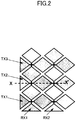
- FIG. 2 is a plan view illustrating an electrode configuration of the touch panel illustrated in FIG. 1 .
- FIG. 3 is a cross-sectional view illustrating a cross-sectional structure of the touch panel illustrated in FIG. 1 .
- the touch panel includes scanning electrodes (TX) for capacitance detection, and detection electrodes (RX) as illustrated in FIG. 2 .
- TX scanning electrodes
- RX detection electrodes
- FIG. 2 the touch panel includes scanning electrodes (TX) for capacitance detection, and detection electrodes (RX) as illustrated in FIG. 2 .
- TX1 to TX3 three of the scanning electrodes (TX), and two (RX1, RX2) of the detection electrodes (RX) are illustrated.
- the numbers of respective electrodes are not limited to those values.
- the touch panel includes a touch panel substrate 41, scanning electrodes (TX) and detection electrodes (RX) which are formed on the touch panel substrate 41, an interlayer insulating film 42 which is formed on the scanning electrodes (TX) and the detection electrodes (RX), and connection portions (STX) which are each formed on the interlayer insulating film 42, and electrically connect the scanning electrodes (TX) to each other.
- TX scanning electrodes
- RX detection electrodes
- STX connection portions
- the touch panel also includes a protective film 43 that is formed on the connection portions (STX), a front window (or protective film) 44 which is arranged on the protective film 43, and a shield transparent electrode (for example, an electrode formed of an ITO (indium tin oxide) film) 45 which is formed on the liquid crystal display panel side of the touch panel substrate 41.
- a protective film 43 that is formed on the connection portions (STX)
- a front window (or protective film) 44 which is arranged on the protective film 43
- a shield transparent electrode for example, an electrode formed of an ITO (indium tin oxide) film
- the respective scanning electrodes (TX) are pulse-driven by a voltage of about 5 to 10 V by a touch panel control IC (DRT).
- a change in the voltage on the detection electrode (RX) is detected to detect a touch position. That is, a capacitance value between each scanning electrode (TX) and each detection electrode (RX) is changed due to a finger touch or the like, and a voltage fluctuation detected by the detection electrode (RX) is changed when the scanning electrode (TX) is pulse-driven.
- the touch position can be detected with measurement of the voltage across the detection electrode (RX).
- the touch panel is located in front of the liquid crystal display panel. Accordingly, when a user watches an image displayed on the liquid crystal display panel, because the touch panel needs to transmit the display image, it is desirable that the touch panel is high in light transmissibility.
- the liquid crystal display panel includes a first substrate (SUB1: also called “TFT substrate”), a second substrate (SUB2; also called “CF substrate”), and liquid crystal (not shown) sandwiched between the first substrate (SUB1) and the second substrate (SUB2).
- first substrate also called “TFT substrate”
- second substrate also called “CF substrate”
- liquid crystal not shown
- the first substrate (SUB1) is larger in area than the second substrate (SUB2), and a liquid crystal driver IC (DRV) is mounted in an area of the first substrate (SUB1) not facing the second substrate (SUB2). Further, a main flexible wiring substrate (MFPC) is mounted in a peripheral part of one side of that area.
- DUV liquid crystal driver IC
- MFPC main flexible wiring substrate
- CT denotes a counter electrode (also called “common electrode”)
- TFPC is a touch panel flexible wiring substrate
- CD is a rear surface transparent conductive film
- 52 is a connection member
- 53 is a connection flexible wiring substrate.
- the counter electrode CT
- the rear surface transparent conductive film CD formed of a transparent conductive film made of, for example, ITO is formed on the substrate where the color filters are disposed.
- FIG. 4 is an exploded perspective view illustrating an outline configuration of the liquid crystal display device in which the touch panel of an in-cell type is incorporated into the liquid crystal display panel.
- SUB1 denotes the first substrate (also called “TFT substrate”)
- SUB2 is the second substrate (also called “CF substrate”)
- CT is the counter electrode (also called “common electrode”)
- DRV is the liquid crystal driver IC
- MFPC is the main flexible wiring substrate
- 44 is the front window
- 53 is the connection flexible wiring substrate.
- the rear surface transparent conductive film (CD) on the second substrate (SUB2) is divided into band-like patterns as the detection electrodes (RX) of the touch panel.
- the counter electrode (CT) formed in the interior of the first substrate (SUB1) is divided into band-like patterns, that is, a plurality of blocks, and also serves as the scanning electrodes (TX) of the touch panel, to thereby eliminate the touch panel substrate (41 in FIG. 1 ).
- a function of the touch panel control IC (DRT) illustrated in FIG. 1 is provided in the interior of the liquid crystal driver IC (DRV).
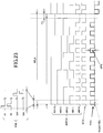
- FIG. 5 is a plan view illustrating an example of a counter electrode divided into a plurality of blocks in the liquid crystal display device.
- SUB1 is the first substrate
- DRV is the liquid crystal driver IC
- CT1 to CT20 are the counter electrodes of the respective blocks divided into the band-like patterns
- GES are scanning line driver circuits incorporated into the liquid crystal display panel
- CTL is counter electrode wirings
- TAM is a terminal portion connected with the main flexible wiring substrate (MFPC)
- AR is a display portion configured by a plurality of pixels which is arranged in a matrix.
- a width of the touch panel scanning electrodes (TX) that conduct AC driving is about 4 to 5 mm. For that reason, the number of scanning electrodes (TX) is increased with the upsized liquid crystal display panel.
- the counter electrode (CT) of 1280 display lines is divided into 20 blocks of CT1 to CT20 (each block is configured by the counter electrode of 64 display lines), and 20 counter electrode wirings (CTL) are required on each of the right and left sides.
- the counter electrodes (CT1 to CT20) of the respective blocks induce the deterioration of the image quality when the voltage fluctuates due to the parasitic capacitance in the display operation.
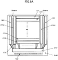
- FIG. 6A is a plan view illustrating a method of driving a divided counter electrode in a liquid crystal display device according to a first embodiment of the present invention.
- the liquid crystal display device is different from the liquid crystal display device illustrated in FIG. 5 in that counter electrode selector circuits (CTSC) that select the respective counter electrodes (CT1 to CT20) divided into 20 blocks according to an address decode system are incorporated into the liquid crystal display panel.
- CTSC counter electrode selector circuits
- the address decode system is applied to a method of selecting the counter electrodes (CT1 to CT20) divided into 20 blocks with the results that two wirings requiring a low resistance are provided for a counter voltage (Vcom) to be supplied to the counter electrodes (CT1 to CT20), and a touch panel scanning voltage (Vstc).
- Vcom counter voltage
- Vstc touch panel scanning voltage
- the touch panel scanning voltage (Vstc) supplies a DC voltage higher than the counter voltage (Vcom) by 5 to 10 V.
- a portion to be scanned is selected according to address signals (addres) which are supplied through address signal lines (Saddres).
- the counter voltage (Vcom) or the touch panel scanning voltage (Vstc) is selectively output to the counter electrode (CT) of the selected block, which also serves as the scanning electrode (TX), according to a touch panel scanning signal (STC).
- the increased wirings are only the address signal lines (S addres), and the number of divisions of the counter electrode used as the touch panel scanning electrodes can be increased while suppressing an increase in the width of the right and left frames of the liquid crystal display panel.
- FIG. 6B is a plan view illustrating a configuration of one sub-pixel in the liquid crystal display panel according to the embodiment of the present invention.
- FIG. 6C is a cross-sectional view illustrating a cross-sectional structure taken along a cut line A-A' illustrated in Fig. 6B .
- FIGS. 6B and 6C a description will be given of a structure of the liquid crystal display panel according to this embodiment with reference to FIGS. 6B and 6C .
- the liquid crystal display panel according to this embodiment is a liquid crystal display panel of the IPS type having planar counter electrodes, and a main surface side of the second substrate (SUB 2) is set as an observation side.
- a liquid crystal layer (LC) side of the second substrate (SUB 2) formed of a transparent substrate such as a glass substrate or a plastic substrate a light blocking membrane (BM), a color filter layer (CF), an overcoat layer (OC), and an alignment film (AL2) are formed in the order from the second substrate (SUB 2) toward a liquid crystal layer (LC). Further, the rear surface transparent conductive film (CD) and a polarization plate (POL2) are formed outside of the second substrate (SUB 2).
- the first substrate (SUB 1) formed of a transparent substrate such as a glass substrate or a plastic substrate, scanning lines (also called “gate lines”) (GL, not shown), a gate insulating film (PAS3), video lines (also called “drain lines” or “source lines”) (DL, not shown), an interlayer insulating film (PAS2), the planar counter electrode (CT), an interlayer insulting film (PAS1), a pixel electrode (PX) formed of a pectinate electrode, and an alignment film (AL1) in the order from the first substrate (SUB 1) toward the liquid crystal layer (LC). Further, a polarization plate (POL1) is formed outside of the first substrate (SUB 1).
- the counter electrode (CT) is formed for each display line.
- the counter electrodes (CT1 to CT20) of the respective blocks illustrated in FIG. 6A are configured so that, for example, the respective counter electrodes (CT) of 64 display lines in series are electrically connected to each other within the liquid crystal display panel.
- reference numeral 2 is a gate electrode
- 3 is a semiconductor layer of a thin film transistor (TFT)
- 4 is a source electrode (also called “drain electrode” when the video line (DL) is called “source line”) .
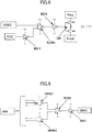
- FIG. 7 is a block diagram illustrating a configuration example of the counter electrode selector circuit (CTSC) illustrated in FIG. 6A .
- the counter electrode selector circuit includes address decoder circuits DEC1 to DEC 20, and selector circuits SCH1 to SCH 20.
- the counter electrodes (CT) for 64 display lines are electrically connected to each other within the liquid crystal display panel as one block so that the scanning electrodes (TX) of the touch panel are arranged at 5 mm pitches, and 1280 display lines are divided into 20 sections.
- the 20 divided counter electrodes (CT1 to CT20) and the address decoder circuits (DEC1 to DEC 20) are allocated to each other in a one-to-one correspondence. Because the number of divisions is 20 blocks, five address signal lines (Sadd) each having 5 bits are required.
- the counter electrode of one block that is, the counter electrode (CT) for 64 display lines, which is selected according to the address signal (addres), conducts AC driving according to the touch panel scanning signal (STC), and the other counter electrodes (CT) output the counter voltage.
- FIG. 8 is a circuit diagram illustrating a circuit configuration of an example of the selector circuit (SCH1 to SCH20) illustrated in FIG. 7 .
- the selector circuit illustrated in FIG. 8 inputs an output (ODEC) of the address decoder circuits (DEC1 to DEC 20), and an inversion signal of the touch panel scanning signal (STC) inverted by an inverter (INV1) to an NOR circuit (NOR1), inverts an output of the NOR circuit (NOR1) by an inverter (INV2), and inputs the inverted signal to a switch circuit (SW).
- the selector circuit selects the touch panel scanning voltage (Vstc) or the counter voltage (Vcom), and outputs the selected voltage to the counter electrodes (CT1 to CT20) of the respective blocks.
- the selector circuit selectively outputs the touch panel scanning voltage (Vstc) and the counter voltage (Vcom) to the counter electrodes of the respective blocks according to the touch panel scanning signal (STC).
- the switch circuit (SW) selects the touch panel scanning voltage (Vstc).
- the switch circuit (SW) selects the counter voltage (Vcom).
- FIG. 9 is a circuit diagram illustrating a circuit configuration of an example of the address decoder circuits (DEC1 to DEC 20) illustrated in FIG. 7 .
- the address decoder circuits receive the address signals or the inversion signals obtained by inverting the address signals by inverters (INV) for the five address signals (addres), and conduct decoding on the basis of the combination of the five address signals (addres), and the inversion signals of the five address signals (addres).
- an address signal (add) of a given combination of the five address signals (addres) and the inversion signals of the five address signals (addres) which have been input to the address decoder circuit is input to NAND circuits (NAND1, NAND2).
- NAND circuits (NAND1, NAND2) Outputs of the NAND circuits (NAND1, NAND2) are input to a NOR circuit (NOR2), and an output of the NOR circuit (NOR2) is inverted by an inverter (INV3) as the output (ODEC) of the address decoder circuit.
- the voltage of L level is output as the output (ODEC) of the address decoder circuit.
- the voltage of H level is output as the output (ODEC) of the address decoder circuit.
- FIG. 10 is a diagram illustrating drive waveforms during touch panel detection and during pixel write in the liquid crystal display device according to the embodiment of the present invention.
- Symbol A in FIG. 10 indicates a voltage waveform of the touch panel scanning voltage (Vstc) to be applied to the counter electrode (CT11) of 641 st to 704 th display lines in an eleventh block among the counter electrodes divided into 20 blocks.
- symbol B in FIG. 10 indicates a waveform of a video voltage to be applied to the odd number video lines (DL)
- C in FIG. 10 indicates a waveform of the video voltage to be applied to the even number video lines (DL).
- D in FIG. 10 denotes a gate signal to be supplied to the gate electrodes of the thin film transistors of the 641 st display line through the 641 st scanning line (GL).
- T1 indicates a touch position detection period
- T2 is a pixel write period.
- the touch position detection period (T1) is set to a period other than the pixel write period (T2). Also, in the touch position detection period (T1), in order to increase the detection sensitivity, scanning is conducted by the scanning electrode (TX) at the same portion by plural times, that is, in FIG. 10 , the touch panel scanning voltage (Vstc) is applied to the counter electrode (CT11) of the 11 th block at plural times. Also, within the pixel write period (T2), not the touch panel scanning voltage (Vstc), but the counter voltage (Vcom) is applied to the counter electrode (CT11) of the 11 th block.
- FIG. 11 is a diagram illustrating timings during touch panel detection and during pixel write in the liquid crystal display device according to the embodiment of the present invention.
- Symbol A in FIG. 11 indicates a pixel write timing from the first display line to the 1280 th display line in a pixel write period (T4) of one frame
- B in FIG. 11 indicates a touch panel detection timing in the counter electrodes (CT1 to CT20) of the respective blocks divided into 20 blocks.
- the counter electrode of an arbitrary display line functions as the scanning electrodes (TX), and the scanning operation during the touch panel detection is conducted at a portion different from that of gate scanning for conducting pixel write.
- T3 denotes a blanking period
- VSYNC is a vertical synchronizing signal
- HSYNC is a horizontal synchronizing signal.
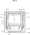
- FIG. 12 is a plan view illustrating a method of driving a divided counter electrode in a liquid crystal display device according to a second embodiment of the present invention.
- the electrode width of the scanning electrodes (TX) is about 4 mm to 5 mm.
- the counter electrodes of two adjacent blocks are driven at a plurality of addresses in an overlap manner with the results that the electrode width of the scanning electrodes (TX) is ensured while enhancing the resolution.
- the counter electrode of the 1280 display lines is divided into 40 blocks of CT1 to CT40 with the counter electrode for 32 display lines arranged at 2.5 mm pitches as one block.
- two blocks such as the counter electrodes of the blocks CT1 and CT2, the counter electrodes of the blocks CT2 and CT3, the counter electrodes of the blocks CT3 and CT4, ... and the counter electrodes of the blocks CT39 and CT40, are scanned at a time to ensure the electrode width of about 5 mm of the scanning electrodes (TX), and enable the scan width of 2.5 mm.
- TX scanning electrodes
- FIG. 13 is a block diagram illustrating a configuration example of the counter electrode selector circuit (CTSC) illustrated in FIG. 12 .
- the counter electrode selector circuit includes address decoder circuits DEC1 to DEC 39, and selector circuits SCH1 to SCH 40.
- the counter electrode is divided into 40 blocks with the counter electrode for 32 display lines arranged at pitches of 2.5 mm as one block.
- FIG. 14 is a circuit diagram illustrating a circuit configuration of an example of the selector circuit (SCH1 to SCH40) illustrated in FIG. 13 .
- the selector circuit illustrated in FIG. 14 is different from the selector circuit illustrated in FIG. 8 in that an AND circuit (AND) that ANDs outputs (ODEC1, ODEC2) of the two adjacent address decoder circuits is added.
- FIG. 15 is a circuit diagram illustrating a circuit configuration of an example of the address decoder circuits (DEC1 to DEC39) illustrated in FIG. 13 .
- the address decoder circuits (DEC1 to DEC 39) illustrated in FIG. 15 receive the address signals or the inversion signals obtained by inverting the address signals by the inverters (INV) for the sixth address signals (addres), and conduct decoding on the basis of the combination of the six address signals (addres), and the inversion signals of the six address signals (addres).
- the circuit configuration of the address decoder circuit illustrated in FIG. 15 is identical with that of the address decoder circuit illustrated in FIG. 9 except that the number of address signals (add) is six, and therefore a detailed description thereof will be omitted.
- the address decode system is applied to a method of selecting the counter electrodes divided into the plurality of blocks.
- the increased wirings are only the address signal lines (Saddres), and an increase in the width of the right and left frames of the liquid crystal display panel can be suppressed.
- the number of address signal lines (Saddres) is increased from four to five. Because the address signal lines (Saddres) normally operate with a relatively high resistance, only one thin wiring is added at each of the right and left sides, and the number of divisions of the touch panel scanning electrodes can be increased while suppressing an increase in the width of the right and left frames of the liquid crystal display panel.
- a touch panel scanning portion is designated by the address decoder circuit. For that reason, the number and position of touch panel scanning can be changed by merely changing the setting of the liquid crystal driver IC (DRV), to thereby flexibly deal with malfunction caused by noise generated by the display operation or the like.
- DUV liquid crystal driver IC
- LCD dynamic operating inspection a method of inspecting the counter electrode selector circuit (CTSC) in a liquid crystal display panel dynamic operating inspection (hereinafter referred to as "LCD dynamic operating inspection").
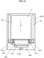
- FIG. 16 is a diagram illustrating an outline of the LCD dynamic operating inspection in the liquid crystal display panel into which a scanning line driver circuit is incorporated.
- liquid crystal display panel in which the first substrate (SUB 1) and the second substrate (SUB 2) have been bonded together, and liquid crystal has been sealed therebetween before the liquid crystal driver IC (DRV) is mounted thereon.
- DUV liquid crystal driver IC
- QD test connection terminals (TAGQ) for the scanning line driver circuits QD test connection terminals (TACQ) for the counter electrodes, and QD test connection terminals (TADQ) for the video lines are formed in an area of the first substrate (SUB 1) which does not face the second substrate (SUB 2).
- TADR is a driver IC connection terminal connected to the respective terminals of the liquid crystal driver IC (DRV)
- STFT is a thin film transistor for dynamic operating inspection.
- a control signal of the scanning line driver circuits, and drive signals such as the signal for the video lines, and the signal for the counter electrode are input to the respective terminals TAGQ, TACQ, and TADQ, whereby the liquid crystal display panel can be lighted before the liquid crystal driver IC (DRV) is mounted thereon.
- DUV liquid crystal driver IC
- TFT thin film transistor
- the control signal of the scanning line driver circuits and the signals for the counter electrodes are input to terminals formed between the scanning line driver circuits (GES) incorporated into the pixel or the liquid crystal display panel, and the connection terminals (or the terminal of the flexible wiring substrate) of the liquid crystal driver IC (DRV) to supply a signal that simulates the drive signal output by the liquid crystal driver IC (DRV).
- GES scanning line driver circuits
- DUV liquid crystal driver IC
- FIG. 17 illustrates an example of the thin film transistors for dynamic operating inspection (STFT).
- drain electrodes (or source electrodes) of the thin film transistor for dynamic operating inspection are connected to the respective driver IC connection terminals (TADR), and collected to a plurality of common lines.
- FIG. 17 illustrates a case in which two systems of the common lines are provided, and different signals can be supplied to odd and even number video lines (DL) from two QD test connection terminals (TADSQ) for the drains (or sources) of the thin film transistors for dynamic operating inspection (STFT).
- TADSQ QD test connection terminals
- a voltage for turning on the thin film transistors for dynamic operating inspection is applied to the gate electrodes of the thin film transistors for dynamic operating inspection (STFT) from a QD test connection terminal (TADGQ) for the gates of the thin film transistors for dynamic operating inspection (STFT).
- the QD test connection terminal (TADGQ) for the gates of the thin film transistors for dynamic operating inspection (STFT) is connected to the driver IC connection terminal (TDR) that outputs a voltage for turning off the thin film transistors for dynamic operating inspection (STFT). For that reason, there is no need to mechanically disconnect the common lines.
- FIG. 18 is a diagram illustrating an outline of the LCD dynamic operating inspection in the liquid crystal display device according to the first embodiment of the present invention.
- FIG. 18 is an outline diagram illustrating the LCD dynamic operating inspection when there is provided the counter electrode selector circuit (CTSC).
- CSC counter electrode selector circuit
- a difference from FIG. 16 resides in that the QD test connection terminals (TACQ) for the counter electrodes is replaced with QD test connection terminals (TACTQ) for driving the counter electrode selector circuit.
- FIG. 19 is a circuit diagram illustrating an equivalent circuit of a pixel in the respective embodiments of the present invention.
- DLx is a video line on an x-row
- GLy is a scanning line on a y-row
- PXxy is a pixel electrode on (x, y)
- CT is an counter electrode
- Cst is a retentive capacitance
- Clc is a liquid crystal capacitance.
- TFT thin film transistors
- TFT thin film transistors
- the retentive capacitance (Cst) and the liquid crystal capacitance (Clc) connected between each pixel electrode (PX) and each counter electrode (CT) are charged with a video voltage and retained to apply the voltage to the liquid crystal for lighting and displaying.
- CTSC counter electrode selector circuit
- FIG. 20 is a diagram illustrating a voltage waveform of a normal liquid crystal drive signal in the general liquid crystal display device.
- FIG. 20 illustrates only a case in which the counter voltage to be applied to the counter electrode (CT) is DC driving, as an example.
- Vcom is a counter voltage to be applied to the counter electrode (CT)
- VDL is a video voltage to be applied to the video lines (DL)
- VPX is a voltage across the pixel electrode (PX)
- VGL is a scanning voltage to be applied to the scanning lines (GL)
- Vhold is a retention voltage to be held by each pixel.
- a scanning voltage (VGL) is input to the gate electrode of the thin film transistors (TFT), and a video voltage (VDL) for applying a desired voltage (VPX) is input to the pixel electrode of the respective pixels.
- the video voltage (VDL) switches positive and negative polarities of the potential to the counter voltage (Vcom) on a frame basis to conduct AC driving.
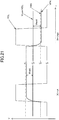
- FIG. 21 is a diagram illustrating a drive waveform for a counter electrode selector circuit inspection in the liquid crystal display device according to the respective embodiments of the present invention.
- VDL video voltage
- Vcom counter voltage
- Vstc touch panel scanning voltage
- the counter electrode selector circuit (CTSC) is selected.
- Vstc touch panel scanning voltage
- Vcom counter voltage
- a voltage difference occurs between the pixel electrode (PX) and the counter electrode (CT), and the retention voltage (Vhold) is held at each pixel.
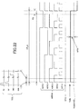
- FIG. 22 is a diagram illustrating an example of a signal waveform of the counter electrode selector circuit (CTSC) for the purpose of inspecting the address decoder circuit according to the respective embodiments of the present invention.
- CTSC counter electrode selector circuit
- FIG. 22 illustrates a case in which the resolution is HD (720RGB ⁇ 1280 pixels), and one block is the counter electrode of 64 display lines.
- the touch panel scanning signal (STC) is fixed to a voltage of H level, and the address signals (addres) of ADR_0 to ADR_4 are input so that the counter electrodes (CT) of the respective blocks are sequentially selected by the address decoder circuits (DEC1 to DEC 20), in synchronism with the timing at which a select scanning voltage (SDL) is sequentially applied to the scanning lines (GL) of, for example, GL1 to GL64.
- the touch panel scanning voltage (Vstc) is applied to the respective pixels at the respective display lines of 1 to 64.
- FIG. 23 is a diagram illustrating an example of a signal waveform of the counter electrode selector circuit (CTSC) for the purpose of inspecting the selector circuit according to the respective embodiments of the present invention.
- CTSC counter electrode selector circuit
- a difference from FIG. 22 resides in that the touch panel scanning signal (STC) switches between H level and L level every 64 display lines. As a result, the voltage across the selector circuits (SCH1 to SCH 20) is switched according to the touch panel scanning signal (STC).
- this inspection method can detect the circuit failure attributable to disconnection or short-circuit, and also can inspect the deterioration of the image quality caused by a counter signal output delay by changing a drive frequency or a drive method (frame/line inversion, etc.) of the liquid crystal display panel. For that reason, the operation margin of the counter electrode selector circuit (CTSC) can be inspected.
- CSC counter electrode selector circuit
Landscapes
- Engineering & Computer Science (AREA)
- Physics & Mathematics (AREA)
- Theoretical Computer Science (AREA)
- General Physics & Mathematics (AREA)
- General Engineering & Computer Science (AREA)
- Nonlinear Science (AREA)
- Crystallography & Structural Chemistry (AREA)
- Chemical & Material Sciences (AREA)
- Human Computer Interaction (AREA)
- Optics & Photonics (AREA)
- Mathematical Physics (AREA)
- Computer Hardware Design (AREA)
- Power Engineering (AREA)
- Geometry (AREA)
- Liquid Crystal (AREA)
- Microelectronics & Electronic Packaging (AREA)
- Control Of Indicators Other Than Cathode Ray Tubes (AREA)
- Liquid Crystal Display Device Control (AREA)
- Devices For Indicating Variable Information By Combining Individual Elements (AREA)
- Position Input By Displaying (AREA)
Applications Claiming Priority (1)
| Application Number | Priority Date | Filing Date | Title |
|---|---|---|---|
| JP2012012262A JP6022164B2 (ja) | 2012-01-24 | 2012-01-24 | 液晶表示装置 |
Publications (3)
| Publication Number | Publication Date |
|---|---|
| EP2620809A2 EP2620809A2 (en) | 2013-07-31 |
| EP2620809A3 EP2620809A3 (en) | 2015-01-07 |
| EP2620809B1 true EP2620809B1 (en) | 2018-04-11 |
Family
ID=47623939
Family Applications (1)
| Application Number | Title | Priority Date | Filing Date |
|---|---|---|---|
| EP13152496.9A Active EP2620809B1 (en) | 2012-01-24 | 2013-01-24 | Liquid crystal display device |
Country Status (6)
| Country | Link |
|---|---|
| US (4) | US9104055B2 (enExample) |
| EP (1) | EP2620809B1 (enExample) |
| JP (1) | JP6022164B2 (enExample) |
| KR (1) | KR101447801B1 (enExample) |
| CN (2) | CN105321493B (enExample) |
| TW (1) | TWI501000B (enExample) |
Families Citing this family (28)
| Publication number | Priority date | Publication date | Assignee | Title |
|---|---|---|---|---|
| KR101441957B1 (ko) * | 2012-05-24 | 2014-09-18 | 엘지디스플레이 주식회사 | 인-셀 터치 구조 액정표시장치 및 이의 구동방법 |
| JP6121812B2 (ja) * | 2013-06-25 | 2017-04-26 | 株式会社ジャパンディスプレイ | タッチパネル付液晶表示装置 |
| KR101681305B1 (ko) | 2014-08-01 | 2016-12-02 | 주식회사 하이딥 | 터치 입력 장치 |
| JP6250342B2 (ja) * | 2013-09-20 | 2017-12-20 | 株式会社ジャパンディスプレイ | 表示装置 |
| KR101641690B1 (ko) | 2013-09-25 | 2016-07-21 | 엘지디스플레이 주식회사 | 터치스크린 일체형 표시장치 |
| KR101623776B1 (ko) * | 2013-12-09 | 2016-06-07 | 엘지디스플레이 주식회사 | 터치 디스플레이 드라이버 집적회로 및 터치 표시장치 |
| CN104916242B (zh) * | 2014-03-14 | 2018-11-13 | 群创光电股份有限公司 | 显示装置及其测试垫 |
| US9024913B1 (en) * | 2014-04-28 | 2015-05-05 | Lg Display Co., Ltd. | Touch sensing device and driving method thereof |
| JP6427337B2 (ja) | 2014-05-16 | 2018-11-21 | 株式会社ジャパンディスプレイ | 表示装置およびその製造方法 |
| JP2015227974A (ja) | 2014-06-02 | 2015-12-17 | 株式会社ジャパンディスプレイ | 表示装置 |
| JP2015227975A (ja) | 2014-06-02 | 2015-12-17 | 株式会社ジャパンディスプレイ | 表示装置およびその製造方法 |
| JP6383573B2 (ja) | 2014-06-05 | 2018-08-29 | 株式会社ジャパンディスプレイ | 表示装置 |
| JP6527343B2 (ja) | 2014-08-01 | 2019-06-05 | 株式会社 ハイディープHiDeep Inc. | タッチ入力装置 |
| US10234339B2 (en) * | 2016-06-02 | 2019-03-19 | Uneo Inc. | Force sensor with noise shielding layer |
| KR102573208B1 (ko) * | 2016-11-30 | 2023-08-30 | 엘지디스플레이 주식회사 | 표시패널 |
| KR20180074956A (ko) * | 2016-12-26 | 2018-07-04 | 주식회사 실리콘웍스 | 패널구동장치 및 패널구동방법 |
| CN107230443B (zh) * | 2017-06-30 | 2019-10-25 | 武汉华星光电技术有限公司 | 内嵌式触摸屏测试电路 |
| JP2019061208A (ja) * | 2017-09-28 | 2019-04-18 | シャープ株式会社 | 表示装置 |
| CN107832547B (zh) * | 2017-11-24 | 2021-01-26 | 京东方科技集团股份有限公司 | 一种柔性面板仿真方法和装置 |
| JP2019139422A (ja) * | 2018-02-08 | 2019-08-22 | 株式会社ジャパンディスプレイ | 検出装置及び検出機能付き表示装置 |
| CN109036236B (zh) * | 2018-09-14 | 2021-10-26 | 京东方科技集团股份有限公司 | 阵列基板检测方法及检测装置 |
| CN109300440B (zh) * | 2018-10-15 | 2020-05-22 | 深圳市华星光电技术有限公司 | 显示装置 |
| US11164897B2 (en) * | 2019-10-28 | 2021-11-02 | Sharp Kabushiki Kaisha | Display device |
| CN111128063B (zh) * | 2020-01-20 | 2021-03-23 | 云谷(固安)科技有限公司 | 显示面板的测试电路、方法及显示面板 |
| JP2020198114A (ja) * | 2020-08-11 | 2020-12-10 | 株式会社半導体エネルギー研究所 | 表示装置 |
| US11841564B2 (en) * | 2021-07-15 | 2023-12-12 | Shanghai Tianma Micro-electronics Co., Ltd. | Display device |
| CN114168017B (zh) * | 2021-12-14 | 2024-02-27 | 武汉天马微电子有限公司 | 显示面板和显示装置 |
| KR20230141981A (ko) * | 2022-03-30 | 2023-10-11 | 삼성디스플레이 주식회사 | 표시 패널의 불량 검사 장치 및 방법 |
Family Cites Families (17)
| Publication number | Priority date | Publication date | Assignee | Title |
|---|---|---|---|---|
| CN1275131C (zh) * | 2001-08-22 | 2006-09-13 | 夏普株式会社 | 触摸传感器、带触摸传感器的显示装置和位置数据产生方法 |
| JP4385967B2 (ja) * | 2005-02-22 | 2009-12-16 | セイコーエプソン株式会社 | 電気光学装置の駆動回路及びこれを備えた電気光学装置、並びに電子機器 |
| KR101142993B1 (ko) * | 2006-02-20 | 2012-05-08 | 삼성전자주식회사 | 표시 장치 및 그의 감지부 검사 방법 |
| JP2007241358A (ja) * | 2006-03-06 | 2007-09-20 | Hitachi Displays Ltd | 画像表示装置 |
| JP4934457B2 (ja) * | 2007-02-20 | 2012-05-16 | 株式会社 日立ディスプレイズ | 画面入力機能付き画像表示装置 |
| CN100582875C (zh) * | 2007-04-13 | 2010-01-20 | 群康科技(深圳)有限公司 | 触摸屏显示装置 |
| CN201126506Y (zh) * | 2007-11-13 | 2008-10-01 | 中山微视显示器有限公司 | 一种内置触控电路的液晶显示屏 |
| JP4816668B2 (ja) * | 2008-03-28 | 2011-11-16 | ソニー株式会社 | タッチセンサ付き表示装置 |
| JP5481040B2 (ja) | 2008-04-11 | 2014-04-23 | 株式会社ジャパンディスプレイ | 表示装置とその駆動方法 |
| JP5203291B2 (ja) * | 2009-05-18 | 2013-06-05 | 株式会社ジャパンディスプレイウェスト | 表示装置および電子機器 |
| JP5203293B2 (ja) * | 2009-05-21 | 2013-06-05 | 株式会社ジャパンディスプレイウェスト | 表示装置および電子機器 |
| JP5178633B2 (ja) * | 2009-05-29 | 2013-04-10 | 株式会社ジャパンディスプレイウェスト | タッチセンサ、表示装置および電子機器 |
| JP5486854B2 (ja) * | 2009-06-29 | 2014-05-07 | 株式会社ジャパンディスプレイ | 情報入力装置、表示装置 |
| JP5439060B2 (ja) * | 2009-06-30 | 2014-03-12 | 株式会社ジャパンディスプレイ | 表示装置 |
| TW201115215A (en) * | 2009-10-23 | 2011-05-01 | Prime View Int Co Ltd | Touch structure and touch display apparatus comprising the same |
| KR101398238B1 (ko) * | 2010-10-01 | 2014-05-22 | 엘지디스플레이 주식회사 | 터치 스크린 패널 일체형 표시장치 |
| KR101230196B1 (ko) * | 2010-10-29 | 2013-02-06 | 삼성디스플레이 주식회사 | 터치 스크린 패널 내장형 액정표시장치 |
-
2012
- 2012-01-24 JP JP2012012262A patent/JP6022164B2/ja active Active
- 2012-12-24 TW TW101149626A patent/TWI501000B/zh active
-
2013
- 2013-01-22 US US13/746,350 patent/US9104055B2/en active Active
- 2013-01-23 KR KR1020130007525A patent/KR101447801B1/ko active Active
- 2013-01-23 CN CN201510809696.7A patent/CN105321493B/zh active Active
- 2013-01-23 CN CN201310038360.6A patent/CN103217823B/zh active Active
- 2013-01-24 EP EP13152496.9A patent/EP2620809B1/en active Active
-
2015
- 2015-06-19 US US14/744,804 patent/US9778501B2/en active Active
-
2017
- 2017-08-31 US US15/691,883 patent/US10302984B2/en active Active
-
2019
- 2019-04-18 US US16/387,690 patent/US10782547B2/en active Active
Non-Patent Citations (1)
| Title |
|---|
| None * |
Also Published As
| Publication number | Publication date |
|---|---|
| US10782547B2 (en) | 2020-09-22 |
| EP2620809A3 (en) | 2015-01-07 |
| US20190250444A1 (en) | 2019-08-15 |
| CN103217823B (zh) | 2015-12-23 |
| CN103217823A (zh) | 2013-07-24 |
| US20150362777A1 (en) | 2015-12-17 |
| CN105321493B (zh) | 2018-01-19 |
| TWI501000B (zh) | 2015-09-21 |
| JP2013152291A (ja) | 2013-08-08 |
| EP2620809A2 (en) | 2013-07-31 |
| US10302984B2 (en) | 2019-05-28 |
| US9104055B2 (en) | 2015-08-11 |
| US9778501B2 (en) | 2017-10-03 |
| TW201331671A (zh) | 2013-08-01 |
| US20180039119A1 (en) | 2018-02-08 |
| US20130188104A1 (en) | 2013-07-25 |
| JP6022164B2 (ja) | 2016-11-09 |
| KR101447801B1 (ko) | 2014-10-06 |
| KR20130086314A (ko) | 2013-08-01 |
| CN105321493A (zh) | 2016-02-10 |
Similar Documents
| Publication | Publication Date | Title |
|---|---|---|
| US10782547B2 (en) | Display device including test connection terminals | |
| US11614817B2 (en) | Display device | |
| JP6618972B2 (ja) | 表示装置 | |
| JP6235678B2 (ja) | 液晶表示装置 | |
| JP6781316B2 (ja) | 表示装置 |
Legal Events
| Date | Code | Title | Description |
|---|---|---|---|
| PUAI | Public reference made under article 153(3) epc to a published international application that has entered the european phase |
Free format text: ORIGINAL CODE: 0009012 |
|
| 17P | Request for examination filed |
Effective date: 20130513 |
|
| AK | Designated contracting states |
Kind code of ref document: A2 Designated state(s): AL AT BE BG CH CY CZ DE DK EE ES FI FR GB GR HR HU IE IS IT LI LT LU LV MC MK MT NL NO PL PT RO RS SE SI SK SM TR |
|
| AX | Request for extension of the european patent |
Extension state: BA ME |
|
| REG | Reference to a national code |
Ref country code: DE Ref legal event code: R079 Ref document number: 602013035609 Country of ref document: DE Free format text: PREVIOUS MAIN CLASS: G02F0001134300 Ipc: G06F0003041000 |
|
| PUAL | Search report despatched |
Free format text: ORIGINAL CODE: 0009013 |
|
| AK | Designated contracting states |
Kind code of ref document: A3 Designated state(s): AL AT BE BG CH CY CZ DE DK EE ES FI FR GB GR HR HU IE IS IT LI LT LU LV MC MK MT NL NO PL PT RO RS SE SI SK SM TR |
|
| AX | Request for extension of the european patent |
Extension state: BA ME |
|
| RIC1 | Information provided on ipc code assigned before grant |
Ipc: G06F 3/041 20060101AFI20141204BHEP |
|
| RAP1 | Party data changed (applicant data changed or rights of an application transferred) |
Owner name: JAPAN DISPLAY INC. |
|
| GRAP | Despatch of communication of intention to grant a patent |
Free format text: ORIGINAL CODE: EPIDOSNIGR1 |
|
| STAA | Information on the status of an ep patent application or granted ep patent |
Free format text: STATUS: GRANT OF PATENT IS INTENDED |
|
| INTG | Intention to grant announced |
Effective date: 20171121 |
|
| GRAS | Grant fee paid |
Free format text: ORIGINAL CODE: EPIDOSNIGR3 |
|
| GRAA | (expected) grant |
Free format text: ORIGINAL CODE: 0009210 |
|
| STAA | Information on the status of an ep patent application or granted ep patent |
Free format text: STATUS: THE PATENT HAS BEEN GRANTED |
|
| AK | Designated contracting states |
Kind code of ref document: B1 Designated state(s): AL AT BE BG CH CY CZ DE DK EE ES FI FR GB GR HR HU IE IS IT LI LT LU LV MC MK MT NL NO PL PT RO RS SE SI SK SM TR |
|
| REG | Reference to a national code |
Ref country code: GB Ref legal event code: FG4D |
|
| REG | Reference to a national code |
Ref country code: CH Ref legal event code: EP |
|
| REG | Reference to a national code |
Ref country code: AT Ref legal event code: REF Ref document number: 988703 Country of ref document: AT Kind code of ref document: T Effective date: 20180415 |
|
| REG | Reference to a national code |
Ref country code: IE Ref legal event code: FG4D |
|
| REG | Reference to a national code |
Ref country code: DE Ref legal event code: R096 Ref document number: 602013035609 Country of ref document: DE |
|
| REG | Reference to a national code |
Ref country code: NL Ref legal event code: MP Effective date: 20180411 |
|
| REG | Reference to a national code |
Ref country code: LT Ref legal event code: MG4D |
|
| PG25 | Lapsed in a contracting state [announced via postgrant information from national office to epo] |
Ref country code: NL Free format text: LAPSE BECAUSE OF FAILURE TO SUBMIT A TRANSLATION OF THE DESCRIPTION OR TO PAY THE FEE WITHIN THE PRESCRIBED TIME-LIMIT Effective date: 20180411 |
|
| PG25 | Lapsed in a contracting state [announced via postgrant information from national office to epo] |
Ref country code: SE Free format text: LAPSE BECAUSE OF FAILURE TO SUBMIT A TRANSLATION OF THE DESCRIPTION OR TO PAY THE FEE WITHIN THE PRESCRIBED TIME-LIMIT Effective date: 20180411 Ref country code: PL Free format text: LAPSE BECAUSE OF FAILURE TO SUBMIT A TRANSLATION OF THE DESCRIPTION OR TO PAY THE FEE WITHIN THE PRESCRIBED TIME-LIMIT Effective date: 20180411 Ref country code: NO Free format text: LAPSE BECAUSE OF FAILURE TO SUBMIT A TRANSLATION OF THE DESCRIPTION OR TO PAY THE FEE WITHIN THE PRESCRIBED TIME-LIMIT Effective date: 20180711 Ref country code: AL Free format text: LAPSE BECAUSE OF FAILURE TO SUBMIT A TRANSLATION OF THE DESCRIPTION OR TO PAY THE FEE WITHIN THE PRESCRIBED TIME-LIMIT Effective date: 20180411 Ref country code: BG Free format text: LAPSE BECAUSE OF FAILURE TO SUBMIT A TRANSLATION OF THE DESCRIPTION OR TO PAY THE FEE WITHIN THE PRESCRIBED TIME-LIMIT Effective date: 20180711 Ref country code: FI Free format text: LAPSE BECAUSE OF FAILURE TO SUBMIT A TRANSLATION OF THE DESCRIPTION OR TO PAY THE FEE WITHIN THE PRESCRIBED TIME-LIMIT Effective date: 20180411 Ref country code: LT Free format text: LAPSE BECAUSE OF FAILURE TO SUBMIT A TRANSLATION OF THE DESCRIPTION OR TO PAY THE FEE WITHIN THE PRESCRIBED TIME-LIMIT Effective date: 20180411 Ref country code: ES Free format text: LAPSE BECAUSE OF FAILURE TO SUBMIT A TRANSLATION OF THE DESCRIPTION OR TO PAY THE FEE WITHIN THE PRESCRIBED TIME-LIMIT Effective date: 20180411 |
|
| PG25 | Lapsed in a contracting state [announced via postgrant information from national office to epo] |
Ref country code: GR Free format text: LAPSE BECAUSE OF FAILURE TO SUBMIT A TRANSLATION OF THE DESCRIPTION OR TO PAY THE FEE WITHIN THE PRESCRIBED TIME-LIMIT Effective date: 20180712 Ref country code: HR Free format text: LAPSE BECAUSE OF FAILURE TO SUBMIT A TRANSLATION OF THE DESCRIPTION OR TO PAY THE FEE WITHIN THE PRESCRIBED TIME-LIMIT Effective date: 20180411 Ref country code: LV Free format text: LAPSE BECAUSE OF FAILURE TO SUBMIT A TRANSLATION OF THE DESCRIPTION OR TO PAY THE FEE WITHIN THE PRESCRIBED TIME-LIMIT Effective date: 20180411 Ref country code: RS Free format text: LAPSE BECAUSE OF FAILURE TO SUBMIT A TRANSLATION OF THE DESCRIPTION OR TO PAY THE FEE WITHIN THE PRESCRIBED TIME-LIMIT Effective date: 20180411 |
|
| REG | Reference to a national code |
Ref country code: AT Ref legal event code: MK05 Ref document number: 988703 Country of ref document: AT Kind code of ref document: T Effective date: 20180411 |
|
| PG25 | Lapsed in a contracting state [announced via postgrant information from national office to epo] |
Ref country code: PT Free format text: LAPSE BECAUSE OF FAILURE TO SUBMIT A TRANSLATION OF THE DESCRIPTION OR TO PAY THE FEE WITHIN THE PRESCRIBED TIME-LIMIT Effective date: 20180813 |
|
| REG | Reference to a national code |
Ref country code: DE Ref legal event code: R097 Ref document number: 602013035609 Country of ref document: DE |
|
| PG25 | Lapsed in a contracting state [announced via postgrant information from national office to epo] |
Ref country code: DK Free format text: LAPSE BECAUSE OF FAILURE TO SUBMIT A TRANSLATION OF THE DESCRIPTION OR TO PAY THE FEE WITHIN THE PRESCRIBED TIME-LIMIT Effective date: 20180411 Ref country code: CZ Free format text: LAPSE BECAUSE OF FAILURE TO SUBMIT A TRANSLATION OF THE DESCRIPTION OR TO PAY THE FEE WITHIN THE PRESCRIBED TIME-LIMIT Effective date: 20180411 Ref country code: AT Free format text: LAPSE BECAUSE OF FAILURE TO SUBMIT A TRANSLATION OF THE DESCRIPTION OR TO PAY THE FEE WITHIN THE PRESCRIBED TIME-LIMIT Effective date: 20180411 Ref country code: EE Free format text: LAPSE BECAUSE OF FAILURE TO SUBMIT A TRANSLATION OF THE DESCRIPTION OR TO PAY THE FEE WITHIN THE PRESCRIBED TIME-LIMIT Effective date: 20180411 Ref country code: RO Free format text: LAPSE BECAUSE OF FAILURE TO SUBMIT A TRANSLATION OF THE DESCRIPTION OR TO PAY THE FEE WITHIN THE PRESCRIBED TIME-LIMIT Effective date: 20180411 Ref country code: SK Free format text: LAPSE BECAUSE OF FAILURE TO SUBMIT A TRANSLATION OF THE DESCRIPTION OR TO PAY THE FEE WITHIN THE PRESCRIBED TIME-LIMIT Effective date: 20180411 |
|
| PLBE | No opposition filed within time limit |
Free format text: ORIGINAL CODE: 0009261 |
|
| STAA | Information on the status of an ep patent application or granted ep patent |
Free format text: STATUS: NO OPPOSITION FILED WITHIN TIME LIMIT |
|
| PG25 | Lapsed in a contracting state [announced via postgrant information from national office to epo] |
Ref country code: IT Free format text: LAPSE BECAUSE OF FAILURE TO SUBMIT A TRANSLATION OF THE DESCRIPTION OR TO PAY THE FEE WITHIN THE PRESCRIBED TIME-LIMIT Effective date: 20180411 Ref country code: SM Free format text: LAPSE BECAUSE OF FAILURE TO SUBMIT A TRANSLATION OF THE DESCRIPTION OR TO PAY THE FEE WITHIN THE PRESCRIBED TIME-LIMIT Effective date: 20180411 |
|
| 26N | No opposition filed |
Effective date: 20190114 |
|
| PG25 | Lapsed in a contracting state [announced via postgrant information from national office to epo] |
Ref country code: SI Free format text: LAPSE BECAUSE OF FAILURE TO SUBMIT A TRANSLATION OF THE DESCRIPTION OR TO PAY THE FEE WITHIN THE PRESCRIBED TIME-LIMIT Effective date: 20180411 |
|
| REG | Reference to a national code |
Ref country code: DE Ref legal event code: R119 Ref document number: 602013035609 Country of ref document: DE |
|
| PG25 | Lapsed in a contracting state [announced via postgrant information from national office to epo] |
Ref country code: MC Free format text: LAPSE BECAUSE OF FAILURE TO SUBMIT A TRANSLATION OF THE DESCRIPTION OR TO PAY THE FEE WITHIN THE PRESCRIBED TIME-LIMIT Effective date: 20180411 |
|
| REG | Reference to a national code |
Ref country code: CH Ref legal event code: PL |
|
| PG25 | Lapsed in a contracting state [announced via postgrant information from national office to epo] |
Ref country code: LU Free format text: LAPSE BECAUSE OF NON-PAYMENT OF DUE FEES Effective date: 20190124 |
|
| REG | Reference to a national code |
Ref country code: BE Ref legal event code: MM Effective date: 20190131 |
|
| REG | Reference to a national code |
Ref country code: IE Ref legal event code: MM4A |
|
| PG25 | Lapsed in a contracting state [announced via postgrant information from national office to epo] |
Ref country code: FR Free format text: LAPSE BECAUSE OF NON-PAYMENT OF DUE FEES Effective date: 20190131 Ref country code: DE Free format text: LAPSE BECAUSE OF NON-PAYMENT OF DUE FEES Effective date: 20190801 |
|
| PG25 | Lapsed in a contracting state [announced via postgrant information from national office to epo] |
Ref country code: BE Free format text: LAPSE BECAUSE OF NON-PAYMENT OF DUE FEES Effective date: 20190131 |
|
| PG25 | Lapsed in a contracting state [announced via postgrant information from national office to epo] |
Ref country code: CH Free format text: LAPSE BECAUSE OF NON-PAYMENT OF DUE FEES Effective date: 20190131 Ref country code: LI Free format text: LAPSE BECAUSE OF NON-PAYMENT OF DUE FEES Effective date: 20190131 |
|
| PG25 | Lapsed in a contracting state [announced via postgrant information from national office to epo] |
Ref country code: IE Free format text: LAPSE BECAUSE OF NON-PAYMENT OF DUE FEES Effective date: 20190124 |
|
| PG25 | Lapsed in a contracting state [announced via postgrant information from national office to epo] |
Ref country code: TR Free format text: LAPSE BECAUSE OF FAILURE TO SUBMIT A TRANSLATION OF THE DESCRIPTION OR TO PAY THE FEE WITHIN THE PRESCRIBED TIME-LIMIT Effective date: 20180411 |
|
| PG25 | Lapsed in a contracting state [announced via postgrant information from national office to epo] |
Ref country code: MT Free format text: LAPSE BECAUSE OF NON-PAYMENT OF DUE FEES Effective date: 20190124 |
|
| PG25 | Lapsed in a contracting state [announced via postgrant information from national office to epo] |
Ref country code: CY Free format text: LAPSE BECAUSE OF FAILURE TO SUBMIT A TRANSLATION OF THE DESCRIPTION OR TO PAY THE FEE WITHIN THE PRESCRIBED TIME-LIMIT Effective date: 20180411 |
|
| PG25 | Lapsed in a contracting state [announced via postgrant information from national office to epo] |
Ref country code: IS Free format text: LAPSE BECAUSE OF FAILURE TO SUBMIT A TRANSLATION OF THE DESCRIPTION OR TO PAY THE FEE WITHIN THE PRESCRIBED TIME-LIMIT Effective date: 20180811 |
|
| PG25 | Lapsed in a contracting state [announced via postgrant information from national office to epo] |
Ref country code: HU Free format text: LAPSE BECAUSE OF FAILURE TO SUBMIT A TRANSLATION OF THE DESCRIPTION OR TO PAY THE FEE WITHIN THE PRESCRIBED TIME-LIMIT; INVALID AB INITIO Effective date: 20130124 |
|
| PG25 | Lapsed in a contracting state [announced via postgrant information from national office to epo] |
Ref country code: MK Free format text: LAPSE BECAUSE OF FAILURE TO SUBMIT A TRANSLATION OF THE DESCRIPTION OR TO PAY THE FEE WITHIN THE PRESCRIBED TIME-LIMIT Effective date: 20180411 |
|
| PGFP | Annual fee paid to national office [announced via postgrant information from national office to epo] |
Ref country code: GB Payment date: 20250128 Year of fee payment: 13 |
|
| REG | Reference to a national code |
Ref country code: GB Ref legal event code: 732E Free format text: REGISTERED BETWEEN 20250724 AND 20250730 |