EP2616865B1 - Imaging optical system - Google Patents
Imaging optical system Download PDFInfo
- Publication number
- EP2616865B1 EP2616865B1 EP11763883.3A EP11763883A EP2616865B1 EP 2616865 B1 EP2616865 B1 EP 2616865B1 EP 11763883 A EP11763883 A EP 11763883A EP 2616865 B1 EP2616865 B1 EP 2616865B1
- Authority
- EP
- European Patent Office
- Prior art keywords
- optical system
- imaging
- reticle
- projection
- mirrors
- Prior art date
- Legal status (The legal status is an assumption and is not a legal conclusion. Google has not performed a legal analysis and makes no representation as to the accuracy of the status listed.)
- Not-in-force
Links
Images


Classifications
-
- G—PHYSICS
- G03—PHOTOGRAPHY; CINEMATOGRAPHY; ANALOGOUS TECHNIQUES USING WAVES OTHER THAN OPTICAL WAVES; ELECTROGRAPHY; HOLOGRAPHY
- G03F—PHOTOMECHANICAL PRODUCTION OF TEXTURED OR PATTERNED SURFACES, e.g. FOR PRINTING, FOR PROCESSING OF SEMICONDUCTOR DEVICES; MATERIALS THEREFOR; ORIGINALS THEREFOR; APPARATUS SPECIALLY ADAPTED THEREFOR
- G03F7/00—Photomechanical, e.g. photolithographic, production of textured or patterned surfaces, e.g. printing surfaces; Materials therefor, e.g. comprising photoresists; Apparatus specially adapted therefor
- G03F7/70—Microphotolithographic exposure; Apparatus therefor
- G03F7/70216—Mask projection systems
- G03F7/70233—Optical aspects of catoptric systems, i.e. comprising only reflective elements, e.g. extreme ultraviolet [EUV] projection systems
-
- G—PHYSICS
- G02—OPTICS
- G02B—OPTICAL ELEMENTS, SYSTEMS OR APPARATUS
- G02B13/00—Optical objectives specially designed for the purposes specified below
- G02B13/08—Anamorphotic objectives
-
- G—PHYSICS
- G02—OPTICS
- G02B—OPTICAL ELEMENTS, SYSTEMS OR APPARATUS
- G02B17/00—Systems with reflecting surfaces, with or without refracting elements
- G02B17/02—Catoptric systems, e.g. image erecting and reversing system
- G02B17/06—Catoptric systems, e.g. image erecting and reversing system using mirrors only, i.e. having only one curved mirror
- G02B17/0647—Catoptric systems, e.g. image erecting and reversing system using mirrors only, i.e. having only one curved mirror using more than three curved mirrors
- G02B17/0663—Catoptric systems, e.g. image erecting and reversing system using mirrors only, i.e. having only one curved mirror using more than three curved mirrors off-axis or unobscured systems in which not all of the mirrors share a common axis of rotational symmetry, e.g. at least one of the mirrors is warped, tilted or decentered with respect to the other elements
-
- G—PHYSICS
- G02—OPTICS
- G02B—OPTICAL ELEMENTS, SYSTEMS OR APPARATUS
- G02B26/00—Optical devices or arrangements for the control of light using movable or deformable optical elements
- G02B26/08—Optical devices or arrangements for the control of light using movable or deformable optical elements for controlling the direction of light
- G02B26/0816—Optical devices or arrangements for the control of light using movable or deformable optical elements for controlling the direction of light by means of one or more reflecting elements
- G02B26/0833—Optical devices or arrangements for the control of light using movable or deformable optical elements for controlling the direction of light by means of one or more reflecting elements the reflecting element being a micromechanical device, e.g. a MEMS mirror, DMD
-
- G—PHYSICS
- G02—OPTICS
- G02B—OPTICAL ELEMENTS, SYSTEMS OR APPARATUS
- G02B5/00—Optical elements other than lenses
- G02B5/08—Mirrors
- G02B5/09—Multifaceted or polygonal mirrors, e.g. polygonal scanning mirrors; Fresnel mirrors
-
- G—PHYSICS
- G03—PHOTOGRAPHY; CINEMATOGRAPHY; ANALOGOUS TECHNIQUES USING WAVES OTHER THAN OPTICAL WAVES; ELECTROGRAPHY; HOLOGRAPHY
- G03F—PHOTOMECHANICAL PRODUCTION OF TEXTURED OR PATTERNED SURFACES, e.g. FOR PRINTING, FOR PROCESSING OF SEMICONDUCTOR DEVICES; MATERIALS THEREFOR; ORIGINALS THEREFOR; APPARATUS SPECIALLY ADAPTED THEREFOR
- G03F7/00—Photomechanical, e.g. photolithographic, production of textured or patterned surfaces, e.g. printing surfaces; Materials therefor, e.g. comprising photoresists; Apparatus specially adapted therefor
- G03F7/70—Microphotolithographic exposure; Apparatus therefor
- G03F7/70058—Mask illumination systems
- G03F7/70091—Illumination settings, i.e. intensity distribution in the pupil plane or angular distribution in the field plane; On-axis or off-axis settings, e.g. annular, dipole or quadrupole settings; Partial coherence control, i.e. sigma or numerical aperture [NA]
- G03F7/701—Off-axis setting using an aperture
-
- G—PHYSICS
- G03—PHOTOGRAPHY; CINEMATOGRAPHY; ANALOGOUS TECHNIQUES USING WAVES OTHER THAN OPTICAL WAVES; ELECTROGRAPHY; HOLOGRAPHY
- G03F—PHOTOMECHANICAL PRODUCTION OF TEXTURED OR PATTERNED SURFACES, e.g. FOR PRINTING, FOR PROCESSING OF SEMICONDUCTOR DEVICES; MATERIALS THEREFOR; ORIGINALS THEREFOR; APPARATUS SPECIALLY ADAPTED THEREFOR
- G03F7/00—Photomechanical, e.g. photolithographic, production of textured or patterned surfaces, e.g. printing surfaces; Materials therefor, e.g. comprising photoresists; Apparatus specially adapted therefor
- G03F7/70—Microphotolithographic exposure; Apparatus therefor
- G03F7/70058—Mask illumination systems
- G03F7/702—Reflective illumination, i.e. reflective optical elements other than folding mirrors, e.g. extreme ultraviolet [EUV] illumination systems
-
- G—PHYSICS
- G03—PHOTOGRAPHY; CINEMATOGRAPHY; ANALOGOUS TECHNIQUES USING WAVES OTHER THAN OPTICAL WAVES; ELECTROGRAPHY; HOLOGRAPHY
- G03F—PHOTOMECHANICAL PRODUCTION OF TEXTURED OR PATTERNED SURFACES, e.g. FOR PRINTING, FOR PROCESSING OF SEMICONDUCTOR DEVICES; MATERIALS THEREFOR; ORIGINALS THEREFOR; APPARATUS SPECIALLY ADAPTED THEREFOR
- G03F7/00—Photomechanical, e.g. photolithographic, production of textured or patterned surfaces, e.g. printing surfaces; Materials therefor, e.g. comprising photoresists; Apparatus specially adapted therefor
- G03F7/70—Microphotolithographic exposure; Apparatus therefor
- G03F7/70216—Mask projection systems
Definitions
- An imaging optical system with at least two part lens systems according to claim 2 of the present invention, of which at least one images anamorphically, is particularly favourable to construct and allows particularly flexible adaptation of the imaging properties to the respective requirements.
- the first, i.e. object-side part lens system images anamorphically. This can ensure that the radiations incident on the object field and reflected thereby do not overlap.
- the second part lens system is also anamorphic. It can also be non-anamorphic.
- a reticle according to claim 10 of the present invention in which the critical dimension in the scanning direction differs from that perpendicular thereto, is particularly well suited for use with an anamorphically imaging projection optical system.
- Both the structures to be imaged on the reticle and the total size thereof are preferably configured in accordance with the different imaging scales in the scanning direction or perpendicular to this.
- the reticle is configured correspondingly larger, in particular in the scanning direction.
- the illumination optical system 4 has an exit pupil, the shape of which is adapted to that of an entry pupil of the projection optical system 9, in particular specifically corresponds to the latter.
- the exit pupil of the illumination optical system 4 is, in particular, elliptical. This can be achieved, in particular, by an elliptically configured pupil facet mirror 18.
- the pupil facets 19 can also be arranged on the pupil facet mirror 18 in such a way that they have an elliptically configured envelope.
- the semi-axes of the elliptical pupil facet mirror 18 have, in particular, two different semi-axis lengths, the greater semi-axis length in particular being at least one and a half times as great, in particular at least twice as great, as the first semi-axis length.
- the semi-axis lengths are, in particular, in the ratio 1:2, 1:3, 1:4, 1:5, 1:6, 1:8, 1:10, 2:3, 2:5 or 3:4.
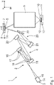
- the reticle holder 8 can be displaced in a controlled manner in such a way that in the projection exposure system, the reticle 7 can be displaced in a displacement direction in the object plane 6. Accordingly, the wafer holder 13 can be displaced in a controlled manner in such a way that the wafer 12 can be displaced in a displacement direction in the image plane 11. As a result, the reticle 7 and the wafer 12 can be scanned, on the one hand, through the object field 5, and, on the other hand, the image field 10.
- the displacement direction in the figures is parallel to the y-direction. It will also be designated the scanning direction below.
- the displacement of the reticle 7 and the wafer 12 in the scanning direction can preferably take place synchronously with respect to one another.
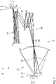
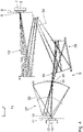
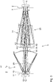
- At least one of the mirrors M1 to M6 is configured to be an anamorphically imaging optical element.
- the projection optical system 9 comprises, in particular, at least one, in particular a plurality of, in particular at least two, in particular at least three, in particular at least four, in particular at least five, in particular at least six, in particular at least seven, in particular at least eight, anamorphically imaging mirrors.
- the mirrors M1 to M5 have reflection faces, which are closed, in other words without a through-opening.
- the mirrors M1, M4 and M6 have concave reflection faces.
- the mirrors M2, M3 and M5 have convex reflection faces.
- c is a constant, which corresponds to the summit of the curve of a corresponding asphere.
- k corresponds to a conical constant of a corresponding asphere.
- C j are the coefficients of the monomials x m y n .
- N radius is a standardisation factor for the coefficients C j .
- the order of the monomial, m + n can be varied as desired. A higher order monomial can lead to a design of the projection optical system with better image error correction, but is, however, more complex to calculate.
- m + n can adopt values between 3 and more than 20.
- the amount in mm is also given, along which the respective mirror, proceeding from a mirror reference design was decentred (Y-decentre) and rotated (X-rotation). This corresponds to a parallel displacement and a tilting in the freeform face design method.
- the displacement takes place in the y-direction here and the titling is about the x-axis.
- the angle of rotation is given here in degrees.
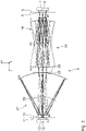
- the optical design data of the projection optical system 9 according to Figs. 6 and 7 will in turn be shown in tables below.
- the mathematical description of the freeform faces corresponds to that which was already described above with reference to the configuration according to Figs. 2 and 3 .
- the structure of the tables with respect to the configuration according to Figs. 6 and 7 also corresponds to that with respect to the configuration according to Figs. 2 and 3 .
- the imaging scales of the projection optical system 9, in particular of the two part lens systems 26, 27, in the direction of the two principal planes, in each case have the same sign. In particular, they both have a positive sign. Therefore no image flip occurs.
- the projection exposure system 1 is used as follows: firstly, the reticle 7 and the wafer 12 are provided. A structure on the reticle 7 is then projected onto a light-sensitive layer of the wafer 12 with the aid of the projection exposure system 1. By developing the light-sensitive layer, a microstructure or nanostructure is then produced on the wafer 12 and therefore the microstructured component, for example a semiconductor component in the form of a highly integrated circuit, is produced.
Landscapes
- Physics & Mathematics (AREA)
- General Physics & Mathematics (AREA)
- Optics & Photonics (AREA)
- Lenses (AREA)
- Exposure And Positioning Against Photoresist Photosensitive Materials (AREA)
- Exposure Of Semiconductors, Excluding Electron Or Ion Beam Exposure (AREA)
Priority Applications (1)
| Application Number | Priority Date | Filing Date | Title |
|---|---|---|---|
| EP22174335.4A EP4071535B1 (en) | 2010-09-15 | 2011-09-13 | Imaging optical system |
Applications Claiming Priority (3)
| Application Number | Priority Date | Filing Date | Title |
|---|---|---|---|
| US38307910P | 2010-09-15 | 2010-09-15 | |
| DE102010040811A DE102010040811A1 (de) | 2010-09-15 | 2010-09-15 | Abbildende Optik |
| PCT/EP2011/065823 WO2012034995A2 (en) | 2010-09-15 | 2011-09-13 | Imaging optical system |
Related Child Applications (2)
| Application Number | Title | Priority Date | Filing Date |
|---|---|---|---|
| EP22174335.4A Division EP4071535B1 (en) | 2010-09-15 | 2011-09-13 | Imaging optical system |
| EP22174335.4A Division-Into EP4071535B1 (en) | 2010-09-15 | 2011-09-13 | Imaging optical system |
Publications (2)
| Publication Number | Publication Date |
|---|---|
| EP2616865A2 EP2616865A2 (en) | 2013-07-24 |
| EP2616865B1 true EP2616865B1 (en) | 2022-06-29 |
Family
ID=44720862
Family Applications (2)
| Application Number | Title | Priority Date | Filing Date |
|---|---|---|---|
| EP11763883.3A Not-in-force EP2616865B1 (en) | 2010-09-15 | 2011-09-13 | Imaging optical system |
| EP22174335.4A Active EP4071535B1 (en) | 2010-09-15 | 2011-09-13 | Imaging optical system |
Family Applications After (1)
| Application Number | Title | Priority Date | Filing Date |
|---|---|---|---|
| EP22174335.4A Active EP4071535B1 (en) | 2010-09-15 | 2011-09-13 | Imaging optical system |
Country Status (7)
| Country | Link |
|---|---|
| US (4) | US9366968B2 (enExample) |
| EP (2) | EP2616865B1 (enExample) |
| JP (2) | JP5938043B2 (enExample) |
| KR (2) | KR102154770B1 (enExample) |
| CN (1) | CN106873135B (enExample) |
| DE (1) | DE102010040811A1 (enExample) |
| WO (1) | WO2012034995A2 (enExample) |
Families Citing this family (43)
| Publication number | Priority date | Publication date | Assignee | Title |
|---|---|---|---|---|
| JPWO2011065374A1 (ja) | 2009-11-24 | 2013-04-18 | 株式会社ニコン | 結像光学系、露光装置、およびデバイス製造方法 |
| DE102010040811A1 (de) | 2010-09-15 | 2012-03-15 | Carl Zeiss Smt Gmbh | Abbildende Optik |
| DE102012208793A1 (de) * | 2012-05-25 | 2013-11-28 | Carl Zeiss Smt Gmbh | Abbildende Optik sowie Projektionsbelichtungsanlage für die Projektionslithographie mit einer derartigen abbildenden Optik |
| DE102014208770A1 (de) * | 2013-07-29 | 2015-01-29 | Carl Zeiss Smt Gmbh | Projektionsoptik zur Abbildung eines Objektfeldes in ein Bildfeld sowie Projektionsbelichtungsanlage mit einer derartigen Projektionsoptik |
| DE102014203188A1 (de) * | 2014-02-21 | 2015-08-27 | Carl Zeiss Smt Gmbh | Verfahren zur Beleuchtung eines Objektfeldes einer Projektionsbelichtungsanlage |
| DE102014203187A1 (de) | 2014-02-21 | 2015-08-27 | Carl Zeiss Smt Gmbh | Beleuchtungsoptik für die Projektionslithografie |
| DE102014203189A1 (de) * | 2014-02-21 | 2015-08-27 | Carl Zeiss Smt Gmbh | Spiegel-Array |
| WO2015124372A2 (en) * | 2014-02-24 | 2015-08-27 | Asml Netherlands B.V. | Lithographic system |
| NL2014267A (en) | 2014-02-24 | 2015-08-25 | Asml Netherlands Bv | Lithographic apparatus and method. |
| DE102014214257A1 (de) | 2014-07-22 | 2016-01-28 | Carl Zeiss Smt Gmbh | Verfahren zum dreidimensionalen Vermessen eines 3D-Luftbildes einer Lithografiemaske |
| WO2016012425A2 (de) | 2014-07-22 | 2016-01-28 | Carl Zeiss Smt Gmbh | Abbildende optik für ein metrologiesystem zur untersuchung einer lithographiemaske |
| DE102014217229B4 (de) | 2014-08-28 | 2023-02-23 | Carl Zeiss Smt Gmbh | Verfahren zum dreidimensionalen Vermessen eines 3D-Luftbildes einer Lithografiemaske sowie Metrologiesystem |
| DE102014218474A1 (de) * | 2014-09-15 | 2016-03-17 | Carl Zeiss Smt Gmbh | Projektionsobjektiv, Projektionsbelichtungsanlage und Projektionsbelichtungsverfahren für die EUV-Mikrolithographie |
| CN107111242B (zh) | 2014-11-18 | 2020-04-24 | 卡尔蔡司Smt有限责任公司 | Euv投射光刻的照明光学单元 |
| DE102014223453A1 (de) | 2014-11-18 | 2016-05-19 | Carl Zeiss Smt Gmbh | Beleuchtungsoptik für die EUV-Projektionslithographie |
| DE102015201138A1 (de) | 2015-01-23 | 2016-01-28 | Carl Zeiss Smt Gmbh | Beleuchtungsoptik für die EUV-Projektionslithografie |
| DE102015203469A1 (de) | 2015-02-26 | 2015-04-23 | Carl Zeiss Smt Gmbh | Verfahren zur Erzeugung einer gekrümmten optischen Spiegelfläche |
| DE102015226531A1 (de) * | 2015-04-14 | 2016-10-20 | Carl Zeiss Smt Gmbh | Abbildende Optik zur Abbildung eines Objektfeldes in ein Bildfeld sowie Projektionsbelichtungsanlage mit einer derartigen abbildenden Optik |
| KR102868300B1 (ko) | 2015-05-28 | 2025-10-13 | 칼 짜이스 에스엠테 게엠베하 | 대물 필드를 이미지 필드 내로 이미징하기 위한 이미징 광학 유닛, 및 이러한 이미징 광학 유닛을 포함하는 투영 노광 장치 |
| DE102015216443A1 (de) | 2015-08-27 | 2017-03-02 | Carl Zeiss Smt Gmbh | Anordnung einer Vorrichtung zum Schutz eines in einer Objektebene anzuordnenden Retikels gegen Verschmutzung |
| DE102016225220A1 (de) | 2016-02-09 | 2017-08-10 | Carl Zeiss Smt Gmbh | Beleuchtungsoptik für die Projektionslithographie sowie optisches System mit einer derartigen Beleuchtungsoptik |
| US9865447B2 (en) * | 2016-03-28 | 2018-01-09 | Kla-Tencor Corporation | High brightness laser-sustained plasma broadband source |
| DE102016205617A1 (de) | 2016-04-05 | 2017-10-05 | Carl Zeiss Smt Gmbh | Projektionsbelichtungsverfahren und Projektionsbelichtungsanlage |
| US11009865B2 (en) | 2016-05-09 | 2021-05-18 | Strong Force Iot Portfolio 2016, Llc | Methods and systems for a noise pattern data marketplace in an industrial internet of things environment |
| DE102016212477A1 (de) | 2016-07-08 | 2018-01-11 | Carl Zeiss Smt Gmbh | Messverfahren und Messsystem zur interferometrischen Vermessung der Abbildungsqualität eines optischen Abbildungssystems |
| US10852528B2 (en) * | 2016-12-20 | 2020-12-01 | Ev Group E. Thallner Gmbh | Method and device for exposure of photosensitive layer |
| KR101950726B1 (ko) | 2016-12-21 | 2019-02-21 | 한남대학교 산학협력단 | 멀티스케일 이미징 시스템 |
| DE102017200935A1 (de) | 2017-01-20 | 2018-07-26 | Carl Zeiss Smt Gmbh | Abbildende Optik zur Führung von EUV-Abbildungslicht sowie Justageanordnung für eine derartige abbildende Optik |
| KR101957357B1 (ko) | 2017-11-16 | 2019-03-12 | 한남대학교 산학협력단 | 단일 미러를 사용한 멀티스케일 이미징 시스템 |
| KR101957353B1 (ko) | 2017-11-16 | 2019-03-12 | 한남대학교 산학협력단 | 미러의 회전이 가능한 멀티스케일 이미징 시스템 |
| DE102018200167A1 (de) | 2018-01-08 | 2019-07-11 | Carl Zeiss Smt Gmbh | Pupillenfacettenspiegel, Beleuchtungsoptik und optisches System für eine Projektionsbelichtungsanlage |
| DE102018207277A1 (de) | 2018-05-09 | 2019-11-14 | Carl Zeiss Smt Gmbh | Lithografiemaske, optisches System zur Übertragung von Original Strukturabschnitten der Lithografiemaske sowie Projektionsoptik zur Abbildung eines Objektfeldes, in dem mindestens ein Original-Strukturabschnitt einer Lithografiemaske anordenbar ist |
| DE102018208373A1 (de) | 2018-05-28 | 2019-06-19 | Carl Zeiss Smt Gmbh | Optisches Element zur Strahlführung von Abbildungslicht bei der Projektionslithographie |
| DE102018210315B4 (de) | 2018-06-25 | 2021-03-18 | Carl Zeiss Smt Gmbh | Verfahren zur Erfassung einer Struktur einer Lithografiemaske sowie Vorrichtung zur Durchführung des Verfahrens |
| DE102018214437A1 (de) | 2018-08-27 | 2018-10-18 | Carl Zeiss Smt Gmbh | Abbildende Optik zur Abbildung eines Objektfeldes in ein Bildfeld sowie Projektionsbelichtungsanlage mit einer derartigen abbildenden Optik |
| DE102019208961A1 (de) | 2019-06-19 | 2020-12-24 | Carl Zeiss Smt Gmbh | Projektionsoptik und Projektionsbelichtungsanlage mit einer solchen Projektionsoptik |
| TWI764353B (zh) * | 2020-11-03 | 2022-05-11 | 大陸商廣州立景創新科技有限公司 | 成像校正單元以及成像模組 |
| DE102021205774A1 (de) | 2021-06-08 | 2022-12-08 | Carl Zeiss Smt Gmbh | Abbildende Optik |
| DE102021205775A1 (de) * | 2021-06-08 | 2022-12-08 | Carl Zeiss Smt Gmbh | Abbildende Optik |
| DE102021213827A1 (de) | 2021-12-06 | 2023-06-07 | Carl Zeiss Smt Gmbh | Verfahren zur Optimierung einer Pupillen-Blendenform zur Nachbildung von Beleuchtungs- und Abbildungseigenschaften eines optischen Produktionssystems bei der Beleuchtung und Abbildung eines Objekts mittels eines optischen Messsystems |
| DE102022209214A1 (de) | 2022-09-05 | 2024-03-07 | Carl Zeiss Smt Gmbh | Einzelspiegel eines Pupillenfacettenspiegels und Pupillenfacettenspiegel für eine Beleuchtungsoptik einer Projektionsbelichtungsanlage |
| DE102023203225A1 (de) | 2023-04-06 | 2024-10-10 | Carl Zeiss Smt Gmbh | Abbildende EUV-Optik zur Abbildung eines Objektfeldes in ein Bildfeld |
| CN116679435B (zh) | 2023-08-03 | 2023-11-24 | 浙江荷湖科技有限公司 | 一种基于双振镜扫描的光场成像系统 |
Citations (3)
| Publication number | Priority date | Publication date | Assignee | Title |
|---|---|---|---|---|
| WO2001009684A1 (de) * | 1999-07-30 | 2001-02-08 | Carl Zeiss | Steuerung der beleuchtungsverteilung in der austrittspupille eines euv-beleuchtungssystems |
| WO2009024164A1 (en) * | 2007-08-20 | 2009-02-26 | Carl Zeiss Smt Ag | Projection objective having mirror elements with reflective coatings |
| US7682031B2 (en) * | 2004-12-23 | 2010-03-23 | Carl Zeiss Smt Ag | Catoptric objectives and systems using catoptric objectives |
Family Cites Families (37)
| Publication number | Priority date | Publication date | Assignee | Title |
|---|---|---|---|---|
| GB1392086A (en) * | 1972-03-29 | 1975-04-23 | Rank Organisation Ltd | Lenses |
| JPH0616485B2 (ja) * | 1989-12-26 | 1994-03-02 | 広島大学長 | 単収束ミラーによる反射型2次元パターン縮小転写法および装置 |
| JP3278303B2 (ja) * | 1993-11-12 | 2002-04-30 | キヤノン株式会社 | 走査型露光装置及び該走査型露光装置を用いるデバイス製造方法 |
| JP3513842B2 (ja) | 1994-12-15 | 2004-03-31 | 株式会社ニコン | 投影露光装置 |
| US5710619A (en) * | 1995-10-31 | 1998-01-20 | Anvik Corporation | Large-area, scan-and-repeat, projection patterning system with unitary stage and magnification control capability |
| JP3975492B2 (ja) * | 1996-06-19 | 2007-09-12 | 株式会社ニコン | 反射光学系およびそれを用いたプロキシミティ露光装置 |
| US5891806A (en) * | 1996-04-22 | 1999-04-06 | Nikon Corporation | Proximity-type microlithography apparatus and method |
| JPH11317344A (ja) * | 1998-04-30 | 1999-11-16 | Nikon Corp | 露光装置 |
| US6859515B2 (en) | 1998-05-05 | 2005-02-22 | Carl-Zeiss-Stiftung Trading | Illumination system, particularly for EUV lithography |
| DE10053587A1 (de) | 2000-10-27 | 2002-05-02 | Zeiss Carl | Beleuchtungssystem mit variabler Einstellung der Ausleuchtung |
| US6924937B2 (en) * | 1998-11-16 | 2005-08-02 | Canon Kabushiki Kaisha | Aberration correcting optical system |
| US6573978B1 (en) * | 1999-01-26 | 2003-06-03 | Mcguire, Jr. James P. | EUV condenser with non-imaging optics |
| DE19931848A1 (de) | 1999-07-09 | 2001-01-11 | Zeiss Carl Fa | Astigmatische Komponenten zur Reduzierung des Wabenaspektverhältnisses bei EUV-Beleuchtungssystemen |
| JP2001189254A (ja) * | 1999-12-28 | 2001-07-10 | Nikon Corp | 露光用レチクル、露光方法並びに半導体素子 |
| JP2001318470A (ja) * | 2000-02-29 | 2001-11-16 | Nikon Corp | 露光装置、マイクロデバイス、フォトマスク、及び露光方法 |
| JP2002048977A (ja) * | 2000-08-01 | 2002-02-15 | Nikon Corp | 反射光学系及びこの光学系を用いたプロキシミティ露光装置 |
| EP1202100A3 (de) | 2000-10-27 | 2005-04-06 | Carl Zeiss SMT AG | Beleuchtungssystem mit reduzierter Wärmebelastung |
| JP4099423B2 (ja) | 2002-03-18 | 2008-06-11 | エーエスエムエル ネザーランズ ビー.ブイ. | リソグラフィ装置およびデバイス製造法 |
| JP2004031808A (ja) | 2002-06-27 | 2004-01-29 | Nikon Corp | 露光装置の投影光学系、該投影光学系を備えた露光装置及び該露光装置を用いた露光方法 |
| CN1474253A (zh) | 2002-08-07 | 2004-02-11 | 联想(北京)有限公司 | 掌上智能设备快捷键的定义方法 |
| JP4428947B2 (ja) * | 2003-06-30 | 2010-03-10 | キヤノン株式会社 | 結像光学系 |
| DE102006043251A1 (de) * | 2005-09-13 | 2007-03-15 | Carl Zeiss Smt Ag | Mikrolithographie-Projektionsobjektiv, Projektionsbelichtungsanlage mit einem derartigen Objektiv, Herstellungsverfahren mikrostrukturierter Bauteile mit einer derartigen Projektionsbelichtungsanlage sowie mit diesem Verfahren hergestelltes Bauteil |
| EP1924888B1 (en) | 2005-09-13 | 2013-07-24 | Carl Zeiss SMT GmbH | Microlithography projection optical system, method for manufacturing a device and method to design an optical surface |
| DE102006031654A1 (de) * | 2006-04-24 | 2007-10-25 | Carl Zeiss Smt Ag | Facettenspiegel mit einer Vielzahl von Spiegelsegmenten |
| JP2008046210A (ja) | 2006-08-11 | 2008-02-28 | Elpida Memory Inc | レチクル及びこれを用いた露光方法及び装置、並びにレチクルのパターン作成方法、パターン形成方法及び半導体装置 |
| EP1930771A1 (en) * | 2006-12-04 | 2008-06-11 | Carl Zeiss SMT AG | Projection objectives having mirror elements with reflective coatings |
| EP1950594A1 (de) * | 2007-01-17 | 2008-07-30 | Carl Zeiss SMT AG | Abbildende Optik, Projektionsbelichtunsanlage für die Mikrolithographie mit einer derartigen abbildenden Optik, Verfahren zur Herstellung eines mikrostrukturierten Bauteils mit einer derartigen Projektionsbelichtungsanlage, durch das Herstellungsverfahren gefertigtes mikrostrukturiertes Bauelement sowie Verwendung einer derartigen abbildenden Optik |
| US7929114B2 (en) * | 2007-01-17 | 2011-04-19 | Carl Zeiss Smt Gmbh | Projection optics for microlithography |
| EP2048540A1 (en) * | 2007-10-09 | 2009-04-15 | Carl Zeiss SMT AG | Microlithographic projection exposure apparatus |
| NL1036108A1 (nl) * | 2007-11-09 | 2009-05-12 | Asml Netherlands Bv | Device Manufacturing Method and Lithographic Apparatus, and Computer Program Product. |
| DE102007062198A1 (de) * | 2007-12-21 | 2009-06-25 | Carl Zeiss Microimaging Gmbh | Katoptrisches Objektiv zur Abbildung eines im Wesentlichen linienförmigen Objektes |
| US20090168034A1 (en) * | 2007-12-28 | 2009-07-02 | Jens Staecker | Methods and Apparatus of Manufacturing a Semiconductor Device |
| DE102008009600A1 (de) | 2008-02-15 | 2009-08-20 | Carl Zeiss Smt Ag | Facettenspiegel zum Einsatz in einer Projektionsbelichtungsanlage für die Mikro-Lithographie |
| DE102009008644A1 (de) | 2009-02-12 | 2010-11-18 | Carl Zeiss Smt Ag | Abbildende Optik sowie Projektionsbelichtungsanlage für die Mikrolithografie mit einer derartigen abbildenden Optik |
| US8743342B2 (en) * | 2009-11-17 | 2014-06-03 | Nikon Corporation | Reflective imaging optical system, exposure apparatus, and method for producing device |
| JPWO2011065374A1 (ja) | 2009-11-24 | 2013-04-18 | 株式会社ニコン | 結像光学系、露光装置、およびデバイス製造方法 |
| DE102010040811A1 (de) | 2010-09-15 | 2012-03-15 | Carl Zeiss Smt Gmbh | Abbildende Optik |
-
2010
- 2010-09-15 DE DE102010040811A patent/DE102010040811A1/de not_active Withdrawn
-
2011
- 2011-09-13 JP JP2013528634A patent/JP5938043B2/ja active Active
- 2011-09-13 EP EP11763883.3A patent/EP2616865B1/en not_active Not-in-force
- 2011-09-13 CN CN201611027506.7A patent/CN106873135B/zh active Active
- 2011-09-13 KR KR1020197019793A patent/KR102154770B1/ko active Active
- 2011-09-13 EP EP22174335.4A patent/EP4071535B1/en active Active
- 2011-09-13 WO PCT/EP2011/065823 patent/WO2012034995A2/en not_active Ceased
- 2011-09-13 KR KR1020137006685A patent/KR102003073B1/ko not_active Expired - Fee Related
-
2013
- 2013-01-18 US US13/744,782 patent/US9366968B2/en active Active
-
2016
- 2016-05-13 JP JP2016096931A patent/JP2016148873A/ja active Pending
- 2016-05-16 US US15/155,356 patent/US9568832B2/en active Active
-
2017
- 2017-02-07 US US15/426,408 patent/US10007187B2/en active Active
-
2018
- 2018-06-18 US US16/010,819 patent/US20190025710A1/en not_active Abandoned
Patent Citations (3)
| Publication number | Priority date | Publication date | Assignee | Title |
|---|---|---|---|---|
| WO2001009684A1 (de) * | 1999-07-30 | 2001-02-08 | Carl Zeiss | Steuerung der beleuchtungsverteilung in der austrittspupille eines euv-beleuchtungssystems |
| US7682031B2 (en) * | 2004-12-23 | 2010-03-23 | Carl Zeiss Smt Ag | Catoptric objectives and systems using catoptric objectives |
| WO2009024164A1 (en) * | 2007-08-20 | 2009-02-26 | Carl Zeiss Smt Ag | Projection objective having mirror elements with reflective coatings |
Non-Patent Citations (2)
| Title |
|---|
| JOSEPH M. HOWARD ET AL: "Anamorphic imaging with three mirrors: a survey", PROCEEDINGS OF SPIE, 1 January 2010 (2010-01-01), pages 76520K - 76520K-7, XP055014862, ISSN: 0277-786X, DOI: 10.1117/12.878972 * |
| RUSSEL HUDYMA: "An Overview of Optical Systems for 30 nm Resolution Lithography at EUV Wavelengths", PROCEEDINGS OF SPIE, IEEE, US, vol. 4832, 1 December 2002 (2002-12-01), pages 137 - 148, XP002370501, ISBN: 978-1-62841-730-2, DOI: 10.1117/12.486427 * |
Also Published As
| Publication number | Publication date |
|---|---|
| CN103109225A (zh) | 2013-05-15 |
| EP4071535B1 (en) | 2024-08-21 |
| KR102003073B1 (ko) | 2019-10-04 |
| US20190025710A1 (en) | 2019-01-24 |
| EP4071535A1 (en) | 2022-10-12 |
| KR102154770B1 (ko) | 2020-09-11 |
| JP5938043B2 (ja) | 2016-06-22 |
| US10007187B2 (en) | 2018-06-26 |
| EP4071535C0 (en) | 2024-08-21 |
| US9366968B2 (en) | 2016-06-14 |
| JP2013541729A (ja) | 2013-11-14 |
| JP2016148873A (ja) | 2016-08-18 |
| US9568832B2 (en) | 2017-02-14 |
| WO2012034995A3 (en) | 2012-05-18 |
| WO2012034995A2 (en) | 2012-03-22 |
| US20170146912A1 (en) | 2017-05-25 |
| CN106873135B (zh) | 2020-04-14 |
| EP2616865A2 (en) | 2013-07-24 |
| KR20130141462A (ko) | 2013-12-26 |
| KR20190086034A (ko) | 2019-07-19 |
| US20130128251A1 (en) | 2013-05-23 |
| CN106873135A (zh) | 2017-06-20 |
| US20160259248A1 (en) | 2016-09-08 |
| DE102010040811A1 (de) | 2012-03-15 |
Similar Documents
| Publication | Publication Date | Title |
|---|---|---|
| EP2616865B1 (en) | Imaging optical system | |
| EP2396700B1 (en) | Imaging optical system and projection exposure installation for microlithography with an imaging optical system of this type | |
| EP2203787B1 (en) | Imaging optical system and projection exposure installation for micro-lithography with an imaging optical system of this type | |
| US9244361B2 (en) | Imaging optical system | |
| EP2255251B1 (en) | Projection objective for microlithography | |
| US9541841B2 (en) | Imaging optical system and projection exposure installation for microlithography including same | |
| CN117441116A (zh) | 成像光学单元 | |
| US20140038110A1 (en) | Imaging optical unit for a projection exposure apparatus | |
| CN103109225B (zh) | 成像光学系统 |
Legal Events
| Date | Code | Title | Description |
|---|---|---|---|
| PUAI | Public reference made under article 153(3) epc to a published international application that has entered the european phase |
Free format text: ORIGINAL CODE: 0009012 |
|
| 17P | Request for examination filed |
Effective date: 20130326 |
|
| AK | Designated contracting states |
Kind code of ref document: A2 Designated state(s): AL AT BE BG CH CY CZ DE DK EE ES FI FR GB GR HR HU IE IS IT LI LT LU LV MC MK MT NL NO PL PT RO RS SE SI SK SM TR |
|
| DAX | Request for extension of the european patent (deleted) | ||
| STAA | Information on the status of an ep patent application or granted ep patent |
Free format text: STATUS: EXAMINATION IS IN PROGRESS |
|
| 17Q | First examination report despatched |
Effective date: 20180625 |
|
| GRAP | Despatch of communication of intention to grant a patent |
Free format text: ORIGINAL CODE: EPIDOSNIGR1 |
|
| STAA | Information on the status of an ep patent application or granted ep patent |
Free format text: STATUS: GRANT OF PATENT IS INTENDED |
|
| INTG | Intention to grant announced |
Effective date: 20220114 |
|
| GRAS | Grant fee paid |
Free format text: ORIGINAL CODE: EPIDOSNIGR3 |
|
| GRAA | (expected) grant |
Free format text: ORIGINAL CODE: 0009210 |
|
| STAA | Information on the status of an ep patent application or granted ep patent |
Free format text: STATUS: THE PATENT HAS BEEN GRANTED |
|
| AK | Designated contracting states |
Kind code of ref document: B1 Designated state(s): AL AT BE BG CH CY CZ DE DK EE ES FI FR GB GR HR HU IE IS IT LI LT LU LV MC MK MT NL NO PL PT RO RS SE SI SK SM TR |
|
| REG | Reference to a national code |
Ref country code: GB Ref legal event code: FG4D |
|
| REG | Reference to a national code |
Ref country code: CH Ref legal event code: EP |
|
| REG | Reference to a national code |
Ref country code: DE Ref legal event code: R096 Ref document number: 602011073060 Country of ref document: DE |
|
| REG | Reference to a national code |
Ref country code: AT Ref legal event code: REF Ref document number: 1501717 Country of ref document: AT Kind code of ref document: T Effective date: 20220715 |
|
| REG | Reference to a national code |
Ref country code: IE Ref legal event code: FG4D |
|
| REG | Reference to a national code |
Ref country code: NL Ref legal event code: FP |
|
| REG | Reference to a national code |
Ref country code: LT Ref legal event code: MG9D |
|
| PG25 | Lapsed in a contracting state [announced via postgrant information from national office to epo] |
Ref country code: SE Free format text: LAPSE BECAUSE OF FAILURE TO SUBMIT A TRANSLATION OF THE DESCRIPTION OR TO PAY THE FEE WITHIN THE PRESCRIBED TIME-LIMIT Effective date: 20220629 Ref country code: NO Free format text: LAPSE BECAUSE OF FAILURE TO SUBMIT A TRANSLATION OF THE DESCRIPTION OR TO PAY THE FEE WITHIN THE PRESCRIBED TIME-LIMIT Effective date: 20220929 Ref country code: LT Free format text: LAPSE BECAUSE OF FAILURE TO SUBMIT A TRANSLATION OF THE DESCRIPTION OR TO PAY THE FEE WITHIN THE PRESCRIBED TIME-LIMIT Effective date: 20220629 Ref country code: HR Free format text: LAPSE BECAUSE OF FAILURE TO SUBMIT A TRANSLATION OF THE DESCRIPTION OR TO PAY THE FEE WITHIN THE PRESCRIBED TIME-LIMIT Effective date: 20220629 Ref country code: GR Free format text: LAPSE BECAUSE OF FAILURE TO SUBMIT A TRANSLATION OF THE DESCRIPTION OR TO PAY THE FEE WITHIN THE PRESCRIBED TIME-LIMIT Effective date: 20220930 Ref country code: FI Free format text: LAPSE BECAUSE OF FAILURE TO SUBMIT A TRANSLATION OF THE DESCRIPTION OR TO PAY THE FEE WITHIN THE PRESCRIBED TIME-LIMIT Effective date: 20220629 Ref country code: BG Free format text: LAPSE BECAUSE OF FAILURE TO SUBMIT A TRANSLATION OF THE DESCRIPTION OR TO PAY THE FEE WITHIN THE PRESCRIBED TIME-LIMIT Effective date: 20220929 |
|
| REG | Reference to a national code |
Ref country code: AT Ref legal event code: MK05 Ref document number: 1501717 Country of ref document: AT Kind code of ref document: T Effective date: 20220629 |
|
| PG25 | Lapsed in a contracting state [announced via postgrant information from national office to epo] |
Ref country code: RS Free format text: LAPSE BECAUSE OF FAILURE TO SUBMIT A TRANSLATION OF THE DESCRIPTION OR TO PAY THE FEE WITHIN THE PRESCRIBED TIME-LIMIT Effective date: 20220629 Ref country code: LV Free format text: LAPSE BECAUSE OF FAILURE TO SUBMIT A TRANSLATION OF THE DESCRIPTION OR TO PAY THE FEE WITHIN THE PRESCRIBED TIME-LIMIT Effective date: 20220629 |
|
| PG25 | Lapsed in a contracting state [announced via postgrant information from national office to epo] |
Ref country code: SM Free format text: LAPSE BECAUSE OF FAILURE TO SUBMIT A TRANSLATION OF THE DESCRIPTION OR TO PAY THE FEE WITHIN THE PRESCRIBED TIME-LIMIT Effective date: 20220629 Ref country code: SK Free format text: LAPSE BECAUSE OF FAILURE TO SUBMIT A TRANSLATION OF THE DESCRIPTION OR TO PAY THE FEE WITHIN THE PRESCRIBED TIME-LIMIT Effective date: 20220629 Ref country code: RO Free format text: LAPSE BECAUSE OF FAILURE TO SUBMIT A TRANSLATION OF THE DESCRIPTION OR TO PAY THE FEE WITHIN THE PRESCRIBED TIME-LIMIT Effective date: 20220629 Ref country code: PT Free format text: LAPSE BECAUSE OF FAILURE TO SUBMIT A TRANSLATION OF THE DESCRIPTION OR TO PAY THE FEE WITHIN THE PRESCRIBED TIME-LIMIT Effective date: 20221031 Ref country code: ES Free format text: LAPSE BECAUSE OF FAILURE TO SUBMIT A TRANSLATION OF THE DESCRIPTION OR TO PAY THE FEE WITHIN THE PRESCRIBED TIME-LIMIT Effective date: 20220629 Ref country code: EE Free format text: LAPSE BECAUSE OF FAILURE TO SUBMIT A TRANSLATION OF THE DESCRIPTION OR TO PAY THE FEE WITHIN THE PRESCRIBED TIME-LIMIT Effective date: 20220629 Ref country code: AT Free format text: LAPSE BECAUSE OF FAILURE TO SUBMIT A TRANSLATION OF THE DESCRIPTION OR TO PAY THE FEE WITHIN THE PRESCRIBED TIME-LIMIT Effective date: 20220629 |
|
| PG25 | Lapsed in a contracting state [announced via postgrant information from national office to epo] |
Ref country code: PL Free format text: LAPSE BECAUSE OF FAILURE TO SUBMIT A TRANSLATION OF THE DESCRIPTION OR TO PAY THE FEE WITHIN THE PRESCRIBED TIME-LIMIT Effective date: 20220629 Ref country code: IS Free format text: LAPSE BECAUSE OF FAILURE TO SUBMIT A TRANSLATION OF THE DESCRIPTION OR TO PAY THE FEE WITHIN THE PRESCRIBED TIME-LIMIT Effective date: 20221029 |
|
| REG | Reference to a national code |
Ref country code: DE Ref legal event code: R097 Ref document number: 602011073060 Country of ref document: DE |
|
| PG25 | Lapsed in a contracting state [announced via postgrant information from national office to epo] |
Ref country code: AL Free format text: LAPSE BECAUSE OF FAILURE TO SUBMIT A TRANSLATION OF THE DESCRIPTION OR TO PAY THE FEE WITHIN THE PRESCRIBED TIME-LIMIT Effective date: 20220629 |
|
| PG25 | Lapsed in a contracting state [announced via postgrant information from national office to epo] |
Ref country code: MC Free format text: LAPSE BECAUSE OF FAILURE TO SUBMIT A TRANSLATION OF THE DESCRIPTION OR TO PAY THE FEE WITHIN THE PRESCRIBED TIME-LIMIT Effective date: 20220629 Ref country code: DK Free format text: LAPSE BECAUSE OF FAILURE TO SUBMIT A TRANSLATION OF THE DESCRIPTION OR TO PAY THE FEE WITHIN THE PRESCRIBED TIME-LIMIT Effective date: 20220629 Ref country code: CZ Free format text: LAPSE BECAUSE OF FAILURE TO SUBMIT A TRANSLATION OF THE DESCRIPTION OR TO PAY THE FEE WITHIN THE PRESCRIBED TIME-LIMIT Effective date: 20220629 |
|
| REG | Reference to a national code |
Ref country code: CH Ref legal event code: PL |
|
| PLBE | No opposition filed within time limit |
Free format text: ORIGINAL CODE: 0009261 |
|
| STAA | Information on the status of an ep patent application or granted ep patent |
Free format text: STATUS: NO OPPOSITION FILED WITHIN TIME LIMIT |
|
| GBPC | Gb: european patent ceased through non-payment of renewal fee |
Effective date: 20220929 |
|
| REG | Reference to a national code |
Ref country code: BE Ref legal event code: MM Effective date: 20220930 |
|
| 26N | No opposition filed |
Effective date: 20230330 |
|
| PG25 | Lapsed in a contracting state [announced via postgrant information from national office to epo] |
Ref country code: LU Free format text: LAPSE BECAUSE OF NON-PAYMENT OF DUE FEES Effective date: 20220913 |
|
| P01 | Opt-out of the competence of the unified patent court (upc) registered |
Effective date: 20230525 |
|
| PG25 | Lapsed in a contracting state [announced via postgrant information from national office to epo] |
Ref country code: LI Free format text: LAPSE BECAUSE OF NON-PAYMENT OF DUE FEES Effective date: 20220930 Ref country code: FR Free format text: LAPSE BECAUSE OF NON-PAYMENT OF DUE FEES Effective date: 20220930 Ref country code: CH Free format text: LAPSE BECAUSE OF NON-PAYMENT OF DUE FEES Effective date: 20220930 |
|
| PG25 | Lapsed in a contracting state [announced via postgrant information from national office to epo] |
Ref country code: SI Free format text: LAPSE BECAUSE OF FAILURE TO SUBMIT A TRANSLATION OF THE DESCRIPTION OR TO PAY THE FEE WITHIN THE PRESCRIBED TIME-LIMIT Effective date: 20220629 |
|
| PG25 | Lapsed in a contracting state [announced via postgrant information from national office to epo] |
Ref country code: BE Free format text: LAPSE BECAUSE OF NON-PAYMENT OF DUE FEES Effective date: 20220930 |
|
| PG25 | Lapsed in a contracting state [announced via postgrant information from national office to epo] |
Ref country code: GB Free format text: LAPSE BECAUSE OF NON-PAYMENT OF DUE FEES Effective date: 20220929 |
|
| PGFP | Annual fee paid to national office [announced via postgrant information from national office to epo] |
Ref country code: NL Payment date: 20230920 Year of fee payment: 13 Ref country code: IE Payment date: 20230920 Year of fee payment: 13 |
|
| PGFP | Annual fee paid to national office [announced via postgrant information from national office to epo] |
Ref country code: DE Payment date: 20230920 Year of fee payment: 13 |
|
| PG25 | Lapsed in a contracting state [announced via postgrant information from national office to epo] |
Ref country code: IT Free format text: LAPSE BECAUSE OF FAILURE TO SUBMIT A TRANSLATION OF THE DESCRIPTION OR TO PAY THE FEE WITHIN THE PRESCRIBED TIME-LIMIT Effective date: 20220629 |
|
| PG25 | Lapsed in a contracting state [announced via postgrant information from national office to epo] |
Ref country code: HU Free format text: LAPSE BECAUSE OF FAILURE TO SUBMIT A TRANSLATION OF THE DESCRIPTION OR TO PAY THE FEE WITHIN THE PRESCRIBED TIME-LIMIT; INVALID AB INITIO Effective date: 20110913 |
|
| PG25 | Lapsed in a contracting state [announced via postgrant information from national office to epo] |
Ref country code: CY Free format text: LAPSE BECAUSE OF FAILURE TO SUBMIT A TRANSLATION OF THE DESCRIPTION OR TO PAY THE FEE WITHIN THE PRESCRIBED TIME-LIMIT Effective date: 20220629 |
|
| PG25 | Lapsed in a contracting state [announced via postgrant information from national office to epo] |
Ref country code: MK Free format text: LAPSE BECAUSE OF FAILURE TO SUBMIT A TRANSLATION OF THE DESCRIPTION OR TO PAY THE FEE WITHIN THE PRESCRIBED TIME-LIMIT Effective date: 20220629 |
|
| PG25 | Lapsed in a contracting state [announced via postgrant information from national office to epo] |
Ref country code: TR Free format text: LAPSE BECAUSE OF FAILURE TO SUBMIT A TRANSLATION OF THE DESCRIPTION OR TO PAY THE FEE WITHIN THE PRESCRIBED TIME-LIMIT Effective date: 20220629 |
|
| PG25 | Lapsed in a contracting state [announced via postgrant information from national office to epo] |
Ref country code: MT Free format text: LAPSE BECAUSE OF FAILURE TO SUBMIT A TRANSLATION OF THE DESCRIPTION OR TO PAY THE FEE WITHIN THE PRESCRIBED TIME-LIMIT Effective date: 20220629 |
|
| PG25 | Lapsed in a contracting state [announced via postgrant information from national office to epo] |
Ref country code: BG Free format text: LAPSE BECAUSE OF FAILURE TO SUBMIT A TRANSLATION OF THE DESCRIPTION OR TO PAY THE FEE WITHIN THE PRESCRIBED TIME-LIMIT Effective date: 20220629 |
|
| PG25 | Lapsed in a contracting state [announced via postgrant information from national office to epo] |
Ref country code: BG Free format text: LAPSE BECAUSE OF FAILURE TO SUBMIT A TRANSLATION OF THE DESCRIPTION OR TO PAY THE FEE WITHIN THE PRESCRIBED TIME-LIMIT Effective date: 20220629 |
|
| REG | Reference to a national code |
Ref country code: DE Ref legal event code: R119 Ref document number: 602011073060 Country of ref document: DE |
|
| REG | Reference to a national code |
Ref country code: NL Ref legal event code: MM Effective date: 20241001 |
|
| PG25 | Lapsed in a contracting state [announced via postgrant information from national office to epo] |
Ref country code: NL Free format text: LAPSE BECAUSE OF NON-PAYMENT OF DUE FEES Effective date: 20241001 |
|
| PG25 | Lapsed in a contracting state [announced via postgrant information from national office to epo] |
Ref country code: DE Free format text: LAPSE BECAUSE OF NON-PAYMENT OF DUE FEES Effective date: 20250401 |
|
| PG25 | Lapsed in a contracting state [announced via postgrant information from national office to epo] |
Ref country code: IE Free format text: LAPSE BECAUSE OF NON-PAYMENT OF DUE FEES Effective date: 20240913 |