EP2614519B1 - Process for treating a substrate using a luminous flux of determined wavelength - Google Patents
Process for treating a substrate using a luminous flux of determined wavelength Download PDFInfo
- Publication number
- EP2614519B1 EP2614519B1 EP11751609.6A EP11751609A EP2614519B1 EP 2614519 B1 EP2614519 B1 EP 2614519B1 EP 11751609 A EP11751609 A EP 11751609A EP 2614519 B1 EP2614519 B1 EP 2614519B1
- Authority
- EP
- European Patent Office
- Prior art keywords
- layer
- substrate
- embedded
- luminous flux
- embedded layer
- Prior art date
- Legal status (The legal status is an assumption and is not a legal conclusion. Google has not performed a legal analysis and makes no representation as to the accuracy of the status listed.)
- Not-in-force
Links
Images

Classifications
-
- H—ELECTRICITY
- H10—SEMICONDUCTOR DEVICES; ELECTRIC SOLID-STATE DEVICES NOT OTHERWISE PROVIDED FOR
- H10D—INORGANIC ELECTRIC SEMICONDUCTOR DEVICES
- H10D62/00—Semiconductor bodies, or regions thereof, of devices having potential barriers
- H10D62/60—Impurity distributions or concentrations
-
- H—ELECTRICITY
- H01—ELECTRIC ELEMENTS
- H01L—SEMICONDUCTOR DEVICES NOT COVERED BY CLASS H10
- H01L21/00—Processes or apparatus adapted for the manufacture or treatment of semiconductor or solid state devices or of parts thereof
- H01L21/02—Manufacture or treatment of semiconductor devices or of parts thereof
- H01L21/04—Manufacture or treatment of semiconductor devices or of parts thereof the devices having potential barriers, e.g. a PN junction, depletion layer or carrier concentration layer
- H01L21/18—Manufacture or treatment of semiconductor devices or of parts thereof the devices having potential barriers, e.g. a PN junction, depletion layer or carrier concentration layer the devices having semiconductor bodies comprising elements of Group IV of the Periodic Table or AIIIBV compounds with or without impurities, e.g. doping materials
- H01L21/26—Bombardment with radiation
- H01L21/263—Bombardment with radiation with high-energy radiation
- H01L21/268—Bombardment with radiation with high-energy radiation using electromagnetic radiation, e.g. laser radiation
-
- H—ELECTRICITY
- H01—ELECTRIC ELEMENTS
- H01L—SEMICONDUCTOR DEVICES NOT COVERED BY CLASS H10
- H01L21/00—Processes or apparatus adapted for the manufacture or treatment of semiconductor or solid state devices or of parts thereof
- H01L21/02—Manufacture or treatment of semiconductor devices or of parts thereof
- H01L21/04—Manufacture or treatment of semiconductor devices or of parts thereof the devices having potential barriers, e.g. a PN junction, depletion layer or carrier concentration layer
- H01L21/18—Manufacture or treatment of semiconductor devices or of parts thereof the devices having potential barriers, e.g. a PN junction, depletion layer or carrier concentration layer the devices having semiconductor bodies comprising elements of Group IV of the Periodic Table or AIIIBV compounds with or without impurities, e.g. doping materials
- H01L21/30—Treatment of semiconductor bodies using processes or apparatus not provided for in groups H01L21/20 - H01L21/26
- H01L21/302—Treatment of semiconductor bodies using processes or apparatus not provided for in groups H01L21/20 - H01L21/26 to change their surface-physical characteristics or shape, e.g. etching, polishing, cutting
-
- H—ELECTRICITY
- H01—ELECTRIC ELEMENTS
- H01L—SEMICONDUCTOR DEVICES NOT COVERED BY CLASS H10
- H01L21/00—Processes or apparatus adapted for the manufacture or treatment of semiconductor or solid state devices or of parts thereof
- H01L21/70—Manufacture or treatment of devices consisting of a plurality of solid state components formed in or on a common substrate or of parts thereof; Manufacture of integrated circuit devices or of parts thereof
- H01L21/71—Manufacture of specific parts of devices defined in group H01L21/70
- H01L21/76—Making of isolation regions between components
- H01L21/762—Dielectric regions, e.g. EPIC dielectric isolation, LOCOS; Trench refilling techniques, SOI technology, use of channel stoppers
- H01L21/7624—Dielectric regions, e.g. EPIC dielectric isolation, LOCOS; Trench refilling techniques, SOI technology, use of channel stoppers using semiconductor on insulator [SOI] technology
- H01L21/76251—Dielectric regions, e.g. EPIC dielectric isolation, LOCOS; Trench refilling techniques, SOI technology, use of channel stoppers using semiconductor on insulator [SOI] technology using bonding techniques
- H01L21/76254—Dielectric regions, e.g. EPIC dielectric isolation, LOCOS; Trench refilling techniques, SOI technology, use of channel stoppers using semiconductor on insulator [SOI] technology using bonding techniques with separation/delamination along an ion implanted layer, e.g. Smart-cut, Unibond
-
- H—ELECTRICITY
- H01—ELECTRIC ELEMENTS
- H01L—SEMICONDUCTOR DEVICES NOT COVERED BY CLASS H10
- H01L21/00—Processes or apparatus adapted for the manufacture or treatment of semiconductor or solid state devices or of parts thereof
- H01L21/70—Manufacture or treatment of devices consisting of a plurality of solid state components formed in or on a common substrate or of parts thereof; Manufacture of integrated circuit devices or of parts thereof
- H01L21/77—Manufacture or treatment of devices consisting of a plurality of solid state components or integrated circuits formed in, or on, a common substrate
- H01L21/78—Manufacture or treatment of devices consisting of a plurality of solid state components or integrated circuits formed in, or on, a common substrate with subsequent division of the substrate into plural individual devices
- H01L21/7806—Manufacture or treatment of devices consisting of a plurality of solid state components or integrated circuits formed in, or on, a common substrate with subsequent division of the substrate into plural individual devices involving the separation of the active layers from a substrate
-
- H—ELECTRICITY
- H10—SEMICONDUCTOR DEVICES; ELECTRIC SOLID-STATE DEVICES NOT OTHERWISE PROVIDED FOR
- H10D—INORGANIC ELECTRIC SEMICONDUCTOR DEVICES
- H10D62/00—Semiconductor bodies, or regions thereof, of devices having potential barriers
- H10D62/10—Shapes, relative sizes or dispositions of the regions of the semiconductor bodies; Shapes of the semiconductor bodies
- H10D62/124—Shapes, relative sizes or dispositions of the regions of semiconductor bodies or of junctions between the regions
-
- H10P34/42—
-
- H10P50/00—
-
- H10P54/00—
-
- H10P95/11—
Definitions
- the present invention relates to a process for treating a substrate by means of a luminous flux of determined wavelength, and a corresponding substrate.
- the process well known under the registered trade mark Smart Cut is a widely used transfer technique which generally consists of implanting a dose of atomic or ionic species in a donor substrate, to create therein an embrittlement zone at a determined depth, delimiting a thin layer to be transferred, adhering the donor substrate on a support substrate or receiver substrate and prompting fracturing of the donor substrate at the level of the embrittlement zone, causing the detachment of the thin layer adhering to the receiver substrate.
- the sub-layer has the particular feature of being absorbent vis-à-vis a luminous flux of predetermined wavelength, this absorption occurring independently of temperature conditions.
- the layer to be heated has as such the particular feature of having a coefficient of absorption of the luminous flux which is low at ambient temperature and increases as this temperature rises.
- the absorbent sub-layer can then be heated by passing through the layer to be heated which is to some degree transparent to a light beam.
- the interface which separates the layer to be heated and the sub-layer is heated and then heats the layers which are adjacent to it, which will in turn make them absorbent such that the layers most distant from the absorbent layer will gradually become more and more absorbent.
- FR 2 938 116 relates to an annealing process for a silicon layer.
- Kunoh et al Fabrication of light emitting diodes transferred onto different substrates by GaN separation technique (Phys. Status Solidi Vol C7, no 7-8 20 May 2010, pages 2091-2093 XP002636008 DOI:10-1002/pssc 200983576) discloses the peeling of a GaN layer formed on an absorbent InGaN layer grown on a GaN substrate.
- This technique therefore rapidly heats localised regions of a substrate to considerable depths which would be heated improperly only if a thermal treatment was undertaken where the sole intervening mechanism would be thermal diffusion, and at the end of a particularly long heating period.
- the thickness of such a layer can typically be in the range of 0.5 - 50 micrometers.
- a first aspect of the present invention relates to a process for treating a substrate by means of a luminous flux of determined wavelength, this substrate comprising an embedded layer which is absorbent, that is, which absorbs said luminous flux independently of the temperature, this embedded layer being interleaved between a first layer, defining a treatment layer, and a second layer, being a first semi-conductive layer having a coefficient of absorption of luminous flux of determined wavelength which is low at ambient temperature and growing as this temperature rises, a process according to which said first layer is irradiated in the direction of said embedded layer by at least one pulse of said luminous flux, of determined wavelength characterised in that
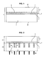
- the substrate shown in Figure 1 is suitable for being treated according to the process of the present invention.
- This substrate 1 comprises an embedded layer 3 which is interleaved between a first layer 2 and a second layer 4.
- the first layer 2 said "treatment” layer, silicon for example, has the particular feature of having a coefficient of absorption of luminous flux of predetermined wavelength, which is low at ambient temperature and growing as this temperature rises.
- this layer comprises lightly doped silicon, for example at a level of around a few 10 15 atoms/cm 3 , then this material is transparent to radiation of laser type emitting in far infrared (for example a wavelength of the order of 10.6 micrometers).
- the above embedded layer 3 is for example a layer which is epitaxied on the layer 2.
- This layer has the particular feature of being significantly absorbent for the above luminous flux and substantially independently of the temperature.
- This layer absorbent when it is a semi-conductor, is to dope it with another atomic species for example.
- this embedded layer can for example be a layer of silicon of a micrometer in thickness doped at a level of the order of 1.10 20 atoms/cm 3 , for example with atoms of boron, phosphorous or arsenic.
- the second layer 4 is as such a layer epitaxied on the preceding one, for example also made of silicon.
- Referenced 5 in this figure is an optional zone of the layer 4, very close to its interface I with the embedded layer, 3 which has the characteristic of being embrittled.
- This localised embrittlement treatment can be carried out in the layer 4 via its rear face 40 by well known embrittlement treatment such as implantation of atomic species combined or not with thermal treatments, or the creation of pores in this zone 5 (treatment of porosification).
- Another example of treatment is the creation of an intermediate layer whereof the material has a mesh parameter different to that of the rest of the layer.
- the layer 4 can be created in the following manner, for example: creation of an epitaxied layer of 2 ⁇ m in thickness of Si-Ge on silicon where the percentage of germanium represents more than 20% and on which another layer of silicon of 20 ⁇ m has been grown by epitaxy, for example.
- the thickness of the second layer 4 is less than that of the first layer 2, their thickness ratio being preferably and typically between 1/2 and 1/100, in such a way that application of the process forming the subject of the invention is also not a result of embrittlement inside the layer 2.
- the corresponding thicknesses of the layers 2 and 4 have been referenced eB and eC in Figure 2 .
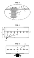
- the process according to the invention consists of irradiating the first layer 2, by its front face 20, by means of a luminous flux whereof the wavelength is determined so that this flux is absorbed by the embedded layer 3, while being transparent, at least in the first instance, for the layer 2.
- the luminous flux is preferably laser radiation in the infrared field.
- infrared radiation passes through the whole layer 2 and is absorbed by the layer 3 which heats locally.
- the latter have a height eA which is a function of the energy output by the radiation luminous and of the duration of application of the latter.
- the present applicant has disclosed the fact that due to the elevation of temperature localised of the layer 2 these thermal pillars, as shown in Figure 3 , dilate and generate constraints C, especially shearing constraints, which locally deform the embedded layer 3, and are transmitted to the second layer 4, near the interface.
- the present process therefore consists of using irradiation to a level of constraints sufficient for initiating incipient fracture, in the second layer 4, in the vicinity of its interface I with the embedded layer 3. At the very least, the process generates structural defects in the layer 4, which make it fragile locally.
- thermal pillars of diameter substantially equal to 50 ⁇ m are produced.
- the temperature of each pillar is brought to a temperature of 1273°K, or a delta T of 1000°K with the ambient temperature.
- the average coefficient of dilation in this temperature range is of 2.5*E-6.
- optimal parameters can be optionally selected by using commercially available simulation software.
- This incipient fracture is all the easier to use, as indicated earlier, if the incipient fracture and/or the embrittlement of the substrate of the layer 4 has been carried out in the zone 5.
- the incipient fracture consists of subjecting the substrate to previous chemical and/or mechanical treatment of its wafer, for example to form an indentation there.
- irradiation in the first instance, near the indentation, then more and more closely to propagate the incipient fracture inherent to the indentation.
- Such a “layer” is made for example by epitaxy on the entire surface of the structure, then localised etching via a mask. After the mask is removed, the second layer 4 is then epitaxied in turn.
- One alternative is to proceed with implantation, for example of arsenic according to a dose of the order of 10 16 atoms/cm 2 via a mask, then annealing at 1050°C for 3 hours.
- the layer 3 in addition to being absorbent, has a thermal dilation coefficient greater than that of the surrounding material, that is, of the material of layers 2 and 4. This boosts the capacity to form incipient fracture within the structure.
- a layer of 2.5 micrometers of silicon strongly doped by atoms of boron at a boron concentration of (10 20 atoms/cm 3 ) is formed on a silicon substrate having a thickness of around 200 micrometers, lightly doped in type n (10 15 atoms/cm 3 ), via an epitaxy technique of CVD type.
- a layer of lightly doped silicon of type n (a few 10 15 atoms/cm 3 ), of 20 micrometers in thickness is cultivated above this layer by epitaxy of CVD type.
- the resulting structure is then soaked for a few minutes in an aqueous solution of ethylene-diamine pyrocatechol, well known to the expert for preferably attacking the silicon doped p.
- the doped layer p is thus attacked chemically at the periphery.
- a laser flux CO 2 is then applied to this structure in the form of a cylindrical flux of 50 microns in diameter of pulses of 600 nanoseconds in duration and energy of 20 J/cm 2 .
- a thermal pillar of cross-section of substantially 50 micrometers and extending from the doped layer p over approximately a height of 60 micrometers is created at each pulse.
- the temperature reached, substantially homogeneous over the entire height of the pillar, is around 1400°C.
- the first thermal pillar is made near (distance less than or equal to a hundred micrometers) the indentation, so as to propagate the incipient fracture inherent to the indentation.
- thermal pillars The whole surface of the substrate then undergoes creation of thermal pillars.
- Each new thermal pillar is built at a distance sufficiently close (for example less than 100 microns) to the point where the preceding pillar was created, so the fracture can be propagated more and more closely.
- This creation of pillars can be carried out continuously, in the sense that the laser beam then emits continuously and is moved at a speed such that the laser flux waits 600 nanoseconds only at each point.
- a layer of 2.5 micrometers of If strongly doped p by boron, at a concentration of 10 20 atoms/cm 3 is formed on a substrate of If in thickness of around 200 micrometers by an epitaxy technique of CVD type.
- a layer of silicon-germanium of 2 micrometers in thickness is cultivated above this layer by epitaxy of CVD type in which, due to dynamic regulation of gaseous flux in the epitaxy machine while this layer is being made, the germanium concentration passes progressively from 5% at the base of the layer to reach 25% in the middle of the thickness of the layer to reduce again to around 5% in the upper part of the layer.
- a lightly doped layer of type n (a few 10 15 atoms/cm 3 ) of 20 micrometers in thickness is made above this layer of Si-Ge by epitaxy.
- the absorbent embedded layer is not necessarily a layer made of doped silicon. It can comprise any semi-conductive layer which has a band gap less than the energy of the photon (component of luminous flux). It can also simply be a layer of oxide.
- the first layer is made of "intrinsic" Si (that is, without doping) of around 20 micrometers in thickness, on which an absorbent layer of 10 micrometers of intrinsic Germanium (non doped) and a layer of SiGe (0.8/0.2) of 50 micrometers (second layer) are cultivated successively.
- the luminous flux is generated by a laser of wavelength equal to 1.08 micrometers.
- the first layer here is a silicon substrate of 500 micrometers in thickness, to which circuits have been transferred (by adhesion and thinning of a plate comprising circuits at its surface).
- the circuit layer of 20 micrometers in thickness constitutes the second layer.
- a planarised layer of oxide has been formed at the surface of the circuits to enable this transfer stage.
- the first layer has also been oxidised. After assembly and thinning, the layer or layers of oxide form the absorbent layer.
- Formation of circuits can be completed after transfer to the first layer, for example by forming interconnections, contacts, etc.
- This layer of circuits (second layer) is then assembled with a final support, and a laser of wavelength of 10.6 micrometers is applied to the exposed face of the first layer, according to the invention, so as to transfer the first layer to the final support.
Landscapes
- Engineering & Computer Science (AREA)
- Physics & Mathematics (AREA)
- Condensed Matter Physics & Semiconductors (AREA)
- General Physics & Mathematics (AREA)
- Manufacturing & Machinery (AREA)
- Computer Hardware Design (AREA)
- Microelectronics & Electronic Packaging (AREA)
- Power Engineering (AREA)
- High Energy & Nuclear Physics (AREA)
- Electromagnetism (AREA)
- Optics & Photonics (AREA)
- Health & Medical Sciences (AREA)
- Toxicology (AREA)
- Recrystallisation Techniques (AREA)
- Crystals, And After-Treatments Of Crystals (AREA)
- Laser Beam Processing (AREA)
Applications Claiming Priority (2)
| Application Number | Priority Date | Filing Date | Title |
|---|---|---|---|
| FR1057211A FR2964788B1 (fr) | 2010-09-10 | 2010-09-10 | Procédé de traitement d'un substrat au moyen d'un flux lumineux de longueur d'onde déterminée, et substrat correspondant |
| PCT/EP2011/065259 WO2012031998A1 (en) | 2010-09-10 | 2011-09-05 | Process for treating a substrate using a luminous flux of determined wavelength, and corresponding substrate |
Publications (2)
| Publication Number | Publication Date |
|---|---|
| EP2614519A1 EP2614519A1 (en) | 2013-07-17 |
| EP2614519B1 true EP2614519B1 (en) | 2015-07-01 |
Family
ID=43920828
Family Applications (1)
| Application Number | Title | Priority Date | Filing Date |
|---|---|---|---|
| EP11751609.6A Not-in-force EP2614519B1 (en) | 2010-09-10 | 2011-09-05 | Process for treating a substrate using a luminous flux of determined wavelength |
Country Status (7)
| Country | Link |
|---|---|
| US (2) | US9190314B2 (enExample) |
| EP (1) | EP2614519B1 (enExample) |
| JP (1) | JP5952281B2 (enExample) |
| KR (1) | KR101918166B1 (enExample) |
| CN (1) | CN103201825A (enExample) |
| FR (1) | FR2964788B1 (enExample) |
| WO (1) | WO2012031998A1 (enExample) |
Families Citing this family (2)
| Publication number | Priority date | Publication date | Assignee | Title |
|---|---|---|---|---|
| FR2964788B1 (fr) | 2010-09-10 | 2015-05-15 | Soitec Silicon On Insulator | Procédé de traitement d'un substrat au moyen d'un flux lumineux de longueur d'onde déterminée, et substrat correspondant |
| FR2978600B1 (fr) | 2011-07-25 | 2014-02-07 | Soitec Silicon On Insulator | Procede et dispositif de fabrication de couche de materiau semi-conducteur |
Family Cites Families (8)
| Publication number | Priority date | Publication date | Assignee | Title |
|---|---|---|---|---|
| FR757986A (fr) | 1932-07-04 | 1934-01-05 | Thomson Houston Comp Francaise | Perfectionnements aux tubes électroniques et à leurs circuits |
| US4234356A (en) * | 1979-06-01 | 1980-11-18 | Bell Telephone Laboratories, Incorporated | Dual wavelength optical annealing of materials |
| US4456490A (en) * | 1983-03-09 | 1984-06-26 | Westinghouse Electric Corp. | Laser annealing of MIS devices by back surface laser treatment |
| JP2008135436A (ja) * | 2006-11-27 | 2008-06-12 | Seiko Epson Corp | 剥離方法、半導体デバイス及び電子機器 |
| JP5286684B2 (ja) * | 2007-03-28 | 2013-09-11 | セイコーエプソン株式会社 | 薄膜層の剥離方法、薄膜デバイスの転写方法 |
| FR2921752B1 (fr) * | 2007-10-01 | 2009-11-13 | Aplinov | Procede de chauffage d'une plaque par un flux lumineux. |
| FR2938116B1 (fr) * | 2008-11-04 | 2011-03-11 | Aplinov | Procede et dispositif de chauffage d'une couche d'une plaque par amorcage et flux lumineux. |
| FR2964788B1 (fr) | 2010-09-10 | 2015-05-15 | Soitec Silicon On Insulator | Procédé de traitement d'un substrat au moyen d'un flux lumineux de longueur d'onde déterminée, et substrat correspondant |
-
2010
- 2010-09-10 FR FR1057211A patent/FR2964788B1/fr not_active Expired - Fee Related
-
2011
- 2011-09-05 WO PCT/EP2011/065259 patent/WO2012031998A1/en not_active Ceased
- 2011-09-05 US US13/818,235 patent/US9190314B2/en not_active Expired - Fee Related
- 2011-09-05 EP EP11751609.6A patent/EP2614519B1/en not_active Not-in-force
- 2011-09-05 CN CN2011800433924A patent/CN103201825A/zh active Pending
- 2011-09-20 JP JP2013527562A patent/JP5952281B2/ja not_active Expired - Fee Related
- 2011-09-20 KR KR1020137005906A patent/KR101918166B1/ko not_active Expired - Fee Related
-
2015
- 2015-11-04 US US14/932,349 patent/US9564496B2/en not_active Expired - Fee Related
Also Published As
| Publication number | Publication date |
|---|---|
| FR2964788B1 (fr) | 2015-05-15 |
| JP2013541197A (ja) | 2013-11-07 |
| WO2012031998A1 (en) | 2012-03-15 |
| JP5952281B2 (ja) | 2016-07-13 |
| KR101918166B1 (ko) | 2018-11-13 |
| KR20140019281A (ko) | 2014-02-14 |
| US20130154065A1 (en) | 2013-06-20 |
| US9190314B2 (en) | 2015-11-17 |
| CN103201825A (zh) | 2013-07-10 |
| FR2964788A1 (fr) | 2012-03-16 |
| EP2614519A1 (en) | 2013-07-17 |
| US20160056247A1 (en) | 2016-02-25 |
| US9564496B2 (en) | 2017-02-07 |
Similar Documents
| Publication | Publication Date | Title |
|---|---|---|
| US8133800B2 (en) | Free-standing thickness of single crystal material and method having carrier lifetimes | |
| EP2019418A2 (en) | Method and structure using selected implant angles for manufacturing free standing films of materials | |
| US20100055874A1 (en) | Layer transfer of films utilizing controlled propagation | |
| US8603896B2 (en) | Method for transferring a monocrystalline semiconductor layer onto a support substrate | |
| US8759196B2 (en) | Method for preparing a substrate by implantation and irradiation | |
| JP2010278338A (ja) | 界面近傍における欠陥密度が低いsos基板 | |
| JP2010278337A (ja) | 表面欠陥密度が少ないsos基板 | |
| EP2614519B1 (en) | Process for treating a substrate using a luminous flux of determined wavelength | |
| EP2689473B1 (en) | Photovoltaic converter with improved emitter structure based on silicon components and a method for production of the photovoltaic converter | |
| Sahoo et al. | Swift heavy ion beam induced recrystallization of amorphous Si layers | |
| JP5518717B2 (ja) | 光束によるウェハの加熱方法 | |
| KR20150030740A (ko) | 〈100〉 실리콘 자기-지지 층의 분리 | |
| JP5650653B2 (ja) | 有向性の剥離を利用する、半導体・オン・インシュレータ構造を生産するための方法および装置 | |
| JP6138931B2 (ja) | 層を転写するためのプロセス | |
| JP5555245B2 (ja) | プライミングおよび光束によって板状体の層を加熱するための方法および装置 | |
| JP5859497B2 (ja) | 界面近傍における欠陥密度が低いsos基板の製造方法 | |
| Sahoo et al. | Epitaxial recrystallization of amorphous Si layers by swift heavy ions | |
| JP2013541197A5 (enExample) | ||
| KR20140115306A (ko) | 광전지 제조 프로세스 | |
| WO2009034358A2 (en) | Hydrogen trapping |
Legal Events
| Date | Code | Title | Description |
|---|---|---|---|
| PUAI | Public reference made under article 153(3) epc to a published international application that has entered the european phase |
Free format text: ORIGINAL CODE: 0009012 |
|
| 17P | Request for examination filed |
Effective date: 20130306 |
|
| AK | Designated contracting states |
Kind code of ref document: A1 Designated state(s): AL AT BE BG CH CY CZ DE DK EE ES FI FR GB GR HR HU IE IS IT LI LT LU LV MC MK MT NL NO PL PT RO RS SE SI SK SM TR |
|
| DAX | Request for extension of the european patent (deleted) | ||
| GRAP | Despatch of communication of intention to grant a patent |
Free format text: ORIGINAL CODE: EPIDOSNIGR1 |
|
| INTG | Intention to grant announced |
Effective date: 20150303 |
|
| GRAS | Grant fee paid |
Free format text: ORIGINAL CODE: EPIDOSNIGR3 |
|
| GRAA | (expected) grant |
Free format text: ORIGINAL CODE: 0009210 |
|
| AK | Designated contracting states |
Kind code of ref document: B1 Designated state(s): AL AT BE BG CH CY CZ DE DK EE ES FI FR GB GR HR HU IE IS IT LI LT LU LV MC MK MT NL NO PL PT RO RS SE SI SK SM TR |
|
| REG | Reference to a national code |
Ref country code: GB Ref legal event code: FG4D |
|
| REG | Reference to a national code |
Ref country code: AT Ref legal event code: REF Ref document number: 734409 Country of ref document: AT Kind code of ref document: T Effective date: 20150715 Ref country code: CH Ref legal event code: EP |
|
| REG | Reference to a national code |
Ref country code: IE Ref legal event code: FG4D |
|
| REG | Reference to a national code |
Ref country code: DE Ref legal event code: R096 Ref document number: 602011017503 Country of ref document: DE |
|
| REG | Reference to a national code |
Ref country code: AT Ref legal event code: MK05 Ref document number: 734409 Country of ref document: AT Kind code of ref document: T Effective date: 20150701 |
|
| REG | Reference to a national code |
Ref country code: NL Ref legal event code: MP Effective date: 20150701 |
|
| REG | Reference to a national code |
Ref country code: LT Ref legal event code: MG4D |
|
| PG25 | Lapsed in a contracting state [announced via postgrant information from national office to epo] |
Ref country code: LT Free format text: LAPSE BECAUSE OF FAILURE TO SUBMIT A TRANSLATION OF THE DESCRIPTION OR TO PAY THE FEE WITHIN THE PRESCRIBED TIME-LIMIT Effective date: 20150701 Ref country code: LV Free format text: LAPSE BECAUSE OF FAILURE TO SUBMIT A TRANSLATION OF THE DESCRIPTION OR TO PAY THE FEE WITHIN THE PRESCRIBED TIME-LIMIT Effective date: 20150701 Ref country code: FI Free format text: LAPSE BECAUSE OF FAILURE TO SUBMIT A TRANSLATION OF THE DESCRIPTION OR TO PAY THE FEE WITHIN THE PRESCRIBED TIME-LIMIT Effective date: 20150701 Ref country code: NO Free format text: LAPSE BECAUSE OF FAILURE TO SUBMIT A TRANSLATION OF THE DESCRIPTION OR TO PAY THE FEE WITHIN THE PRESCRIBED TIME-LIMIT Effective date: 20151001 |
|
| PG25 | Lapsed in a contracting state [announced via postgrant information from national office to epo] |
Ref country code: AT Free format text: LAPSE BECAUSE OF FAILURE TO SUBMIT A TRANSLATION OF THE DESCRIPTION OR TO PAY THE FEE WITHIN THE PRESCRIBED TIME-LIMIT Effective date: 20150701 Ref country code: PL Free format text: LAPSE BECAUSE OF FAILURE TO SUBMIT A TRANSLATION OF THE DESCRIPTION OR TO PAY THE FEE WITHIN THE PRESCRIBED TIME-LIMIT Effective date: 20150701 Ref country code: HR Free format text: LAPSE BECAUSE OF FAILURE TO SUBMIT A TRANSLATION OF THE DESCRIPTION OR TO PAY THE FEE WITHIN THE PRESCRIBED TIME-LIMIT Effective date: 20150701 Ref country code: IS Free format text: LAPSE BECAUSE OF FAILURE TO SUBMIT A TRANSLATION OF THE DESCRIPTION OR TO PAY THE FEE WITHIN THE PRESCRIBED TIME-LIMIT Effective date: 20151101 Ref country code: RS Free format text: LAPSE BECAUSE OF FAILURE TO SUBMIT A TRANSLATION OF THE DESCRIPTION OR TO PAY THE FEE WITHIN THE PRESCRIBED TIME-LIMIT Effective date: 20150701 Ref country code: SE Free format text: LAPSE BECAUSE OF FAILURE TO SUBMIT A TRANSLATION OF THE DESCRIPTION OR TO PAY THE FEE WITHIN THE PRESCRIBED TIME-LIMIT Effective date: 20150701 Ref country code: ES Free format text: LAPSE BECAUSE OF FAILURE TO SUBMIT A TRANSLATION OF THE DESCRIPTION OR TO PAY THE FEE WITHIN THE PRESCRIBED TIME-LIMIT Effective date: 20150701 Ref country code: PT Free format text: LAPSE BECAUSE OF FAILURE TO SUBMIT A TRANSLATION OF THE DESCRIPTION OR TO PAY THE FEE WITHIN THE PRESCRIBED TIME-LIMIT Effective date: 20151102 |
|
| REG | Reference to a national code |
Ref country code: DE Ref legal event code: R097 Ref document number: 602011017503 Country of ref document: DE |
|
| PG25 | Lapsed in a contracting state [announced via postgrant information from national office to epo] |
Ref country code: CZ Free format text: LAPSE BECAUSE OF FAILURE TO SUBMIT A TRANSLATION OF THE DESCRIPTION OR TO PAY THE FEE WITHIN THE PRESCRIBED TIME-LIMIT Effective date: 20150701 Ref country code: LU Free format text: LAPSE BECAUSE OF FAILURE TO SUBMIT A TRANSLATION OF THE DESCRIPTION OR TO PAY THE FEE WITHIN THE PRESCRIBED TIME-LIMIT Effective date: 20150905 Ref country code: SK Free format text: LAPSE BECAUSE OF FAILURE TO SUBMIT A TRANSLATION OF THE DESCRIPTION OR TO PAY THE FEE WITHIN THE PRESCRIBED TIME-LIMIT Effective date: 20150701 Ref country code: DK Free format text: LAPSE BECAUSE OF FAILURE TO SUBMIT A TRANSLATION OF THE DESCRIPTION OR TO PAY THE FEE WITHIN THE PRESCRIBED TIME-LIMIT Effective date: 20150701 Ref country code: MC Free format text: LAPSE BECAUSE OF FAILURE TO SUBMIT A TRANSLATION OF THE DESCRIPTION OR TO PAY THE FEE WITHIN THE PRESCRIBED TIME-LIMIT Effective date: 20150701 Ref country code: IT Free format text: LAPSE BECAUSE OF FAILURE TO SUBMIT A TRANSLATION OF THE DESCRIPTION OR TO PAY THE FEE WITHIN THE PRESCRIBED TIME-LIMIT Effective date: 20150701 Ref country code: EE Free format text: LAPSE BECAUSE OF FAILURE TO SUBMIT A TRANSLATION OF THE DESCRIPTION OR TO PAY THE FEE WITHIN THE PRESCRIBED TIME-LIMIT Effective date: 20150701 |
|
| REG | Reference to a national code |
Ref country code: CH Ref legal event code: PL |
|
| PLBE | No opposition filed within time limit |
Free format text: ORIGINAL CODE: 0009261 |
|
| STAA | Information on the status of an ep patent application or granted ep patent |
Free format text: STATUS: NO OPPOSITION FILED WITHIN TIME LIMIT |
|
| PG25 | Lapsed in a contracting state [announced via postgrant information from national office to epo] |
Ref country code: RO Free format text: LAPSE BECAUSE OF FAILURE TO SUBMIT A TRANSLATION OF THE DESCRIPTION OR TO PAY THE FEE WITHIN THE PRESCRIBED TIME-LIMIT Effective date: 20150701 |
|
| 26N | No opposition filed |
Effective date: 20160404 |
|
| REG | Reference to a national code |
Ref country code: IE Ref legal event code: MM4A |
|
| PG25 | Lapsed in a contracting state [announced via postgrant information from national office to epo] |
Ref country code: CH Free format text: LAPSE BECAUSE OF NON-PAYMENT OF DUE FEES Effective date: 20150930 Ref country code: LI Free format text: LAPSE BECAUSE OF NON-PAYMENT OF DUE FEES Effective date: 20150930 Ref country code: IE Free format text: LAPSE BECAUSE OF NON-PAYMENT OF DUE FEES Effective date: 20150905 |
|
| REG | Reference to a national code |
Ref country code: FR Ref legal event code: PLFP Year of fee payment: 6 |
|
| PG25 | Lapsed in a contracting state [announced via postgrant information from national office to epo] |
Ref country code: SI Free format text: LAPSE BECAUSE OF FAILURE TO SUBMIT A TRANSLATION OF THE DESCRIPTION OR TO PAY THE FEE WITHIN THE PRESCRIBED TIME-LIMIT Effective date: 20150701 |
|
| PG25 | Lapsed in a contracting state [announced via postgrant information from national office to epo] |
Ref country code: BE Free format text: LAPSE BECAUSE OF FAILURE TO SUBMIT A TRANSLATION OF THE DESCRIPTION OR TO PAY THE FEE WITHIN THE PRESCRIBED TIME-LIMIT Effective date: 20150701 |
|
| PG25 | Lapsed in a contracting state [announced via postgrant information from national office to epo] |
Ref country code: MT Free format text: LAPSE BECAUSE OF FAILURE TO SUBMIT A TRANSLATION OF THE DESCRIPTION OR TO PAY THE FEE WITHIN THE PRESCRIBED TIME-LIMIT Effective date: 20150701 |
|
| PG25 | Lapsed in a contracting state [announced via postgrant information from national office to epo] |
Ref country code: BG Free format text: LAPSE BECAUSE OF FAILURE TO SUBMIT A TRANSLATION OF THE DESCRIPTION OR TO PAY THE FEE WITHIN THE PRESCRIBED TIME-LIMIT Effective date: 20150701 Ref country code: HU Free format text: LAPSE BECAUSE OF FAILURE TO SUBMIT A TRANSLATION OF THE DESCRIPTION OR TO PAY THE FEE WITHIN THE PRESCRIBED TIME-LIMIT; INVALID AB INITIO Effective date: 20110905 Ref country code: SM Free format text: LAPSE BECAUSE OF FAILURE TO SUBMIT A TRANSLATION OF THE DESCRIPTION OR TO PAY THE FEE WITHIN THE PRESCRIBED TIME-LIMIT Effective date: 20150701 |
|
| PG25 | Lapsed in a contracting state [announced via postgrant information from national office to epo] |
Ref country code: GR Free format text: LAPSE BECAUSE OF FAILURE TO SUBMIT A TRANSLATION OF THE DESCRIPTION OR TO PAY THE FEE WITHIN THE PRESCRIBED TIME-LIMIT Effective date: 20150701 Ref country code: NL Free format text: LAPSE BECAUSE OF FAILURE TO SUBMIT A TRANSLATION OF THE DESCRIPTION OR TO PAY THE FEE WITHIN THE PRESCRIBED TIME-LIMIT Effective date: 20150701 Ref country code: CY Free format text: LAPSE BECAUSE OF FAILURE TO SUBMIT A TRANSLATION OF THE DESCRIPTION OR TO PAY THE FEE WITHIN THE PRESCRIBED TIME-LIMIT Effective date: 20150701 |
|
| REG | Reference to a national code |
Ref country code: FR Ref legal event code: PLFP Year of fee payment: 7 |
|
| PG25 | Lapsed in a contracting state [announced via postgrant information from national office to epo] |
Ref country code: MK Free format text: LAPSE BECAUSE OF FAILURE TO SUBMIT A TRANSLATION OF THE DESCRIPTION OR TO PAY THE FEE WITHIN THE PRESCRIBED TIME-LIMIT Effective date: 20150701 Ref country code: TR Free format text: LAPSE BECAUSE OF FAILURE TO SUBMIT A TRANSLATION OF THE DESCRIPTION OR TO PAY THE FEE WITHIN THE PRESCRIBED TIME-LIMIT Effective date: 20150701 |
|
| REG | Reference to a national code |
Ref country code: FR Ref legal event code: PLFP Year of fee payment: 8 |
|
| PG25 | Lapsed in a contracting state [announced via postgrant information from national office to epo] |
Ref country code: AL Free format text: LAPSE BECAUSE OF FAILURE TO SUBMIT A TRANSLATION OF THE DESCRIPTION OR TO PAY THE FEE WITHIN THE PRESCRIBED TIME-LIMIT Effective date: 20150701 |
|
| PGFP | Annual fee paid to national office [announced via postgrant information from national office to epo] |
Ref country code: DE Payment date: 20190820 Year of fee payment: 9 Ref country code: FR Payment date: 20190820 Year of fee payment: 9 |
|
| PGFP | Annual fee paid to national office [announced via postgrant information from national office to epo] |
Ref country code: GB Payment date: 20190820 Year of fee payment: 9 |
|
| REG | Reference to a national code |
Ref country code: DE Ref legal event code: R119 Ref document number: 602011017503 Country of ref document: DE |
|
| GBPC | Gb: european patent ceased through non-payment of renewal fee |
Effective date: 20200905 |
|
| PG25 | Lapsed in a contracting state [announced via postgrant information from national office to epo] |
Ref country code: DE Free format text: LAPSE BECAUSE OF NON-PAYMENT OF DUE FEES Effective date: 20210401 Ref country code: FR Free format text: LAPSE BECAUSE OF NON-PAYMENT OF DUE FEES Effective date: 20200930 |
|
| PG25 | Lapsed in a contracting state [announced via postgrant information from national office to epo] |
Ref country code: GB Free format text: LAPSE BECAUSE OF NON-PAYMENT OF DUE FEES Effective date: 20200905 |