EP2613452B1 - Digitale filtervorrichtung, digitales filterverfahren und steuerprogramm für die digitale filtervorrichtung - Google Patents
Digitale filtervorrichtung, digitales filterverfahren und steuerprogramm für die digitale filtervorrichtung Download PDFInfo
- Publication number
- EP2613452B1 EP2613452B1 EP11821630.8A EP11821630A EP2613452B1 EP 2613452 B1 EP2613452 B1 EP 2613452B1 EP 11821630 A EP11821630 A EP 11821630A EP 2613452 B1 EP2613452 B1 EP 2613452B1
- Authority
- EP
- European Patent Office
- Prior art keywords
- filter
- distortion compensation
- digital
- distortion
- filter coefficient
- Prior art date
- Legal status (The legal status is an assumption and is not a legal conclusion. Google has not performed a legal analysis and makes no representation as to the accuracy of the status listed.)
- Active
Links
- 238000000034 method Methods 0.000 title claims description 16
- 238000001914 filtration Methods 0.000 title claims description 4
- 238000012545 processing Methods 0.000 claims description 37
- 238000006243 chemical reaction Methods 0.000 claims description 15
- 230000008859 change Effects 0.000 claims description 6
- 230000004044 response Effects 0.000 claims description 4
- 238000012544 monitoring process Methods 0.000 claims 2
- 230000001427 coherent effect Effects 0.000 description 19
- 238000010586 diagram Methods 0.000 description 18
- 239000006185 dispersion Substances 0.000 description 17
- 230000006870 function Effects 0.000 description 14
- 230000010287 polarization Effects 0.000 description 14
- 230000003287 optical effect Effects 0.000 description 13
- 238000005070 sampling Methods 0.000 description 12
- 230000005540 biological transmission Effects 0.000 description 10
- 230000003044 adaptive effect Effects 0.000 description 9
- 230000006866 deterioration Effects 0.000 description 9
- 238000004891 communication Methods 0.000 description 8
- 230000008569 process Effects 0.000 description 6
- 238000004364 calculation method Methods 0.000 description 5
- 238000005516 engineering process Methods 0.000 description 4
- 230000010363 phase shift Effects 0.000 description 4
- 230000008901 benefit Effects 0.000 description 2
- 238000000605 extraction Methods 0.000 description 2
- 101100379079 Emericella variicolor andA gene Proteins 0.000 description 1
- 230000002238 attenuated effect Effects 0.000 description 1
- 230000001419 dependent effect Effects 0.000 description 1
- 238000011982 device technology Methods 0.000 description 1
- 230000000694 effects Effects 0.000 description 1
- 230000006872 improvement Effects 0.000 description 1
- 239000013307 optical fiber Substances 0.000 description 1
- 238000012887 quadratic function Methods 0.000 description 1
- 230000035945 sensitivity Effects 0.000 description 1
- 239000000758 substrate Substances 0.000 description 1
- 230000001360 synchronised effect Effects 0.000 description 1
- 238000012549 training Methods 0.000 description 1
Images


Classifications
-
- H—ELECTRICITY
- H04—ELECTRIC COMMUNICATION TECHNIQUE
- H04B—TRANSMISSION
- H04B10/00—Transmission systems employing electromagnetic waves other than radio-waves, e.g. infrared, visible or ultraviolet light, or employing corpuscular radiation, e.g. quantum communication
- H04B10/60—Receivers
- H04B10/61—Coherent receivers
- H04B10/616—Details of the electronic signal processing in coherent optical receivers
-
- H—ELECTRICITY
- H03—ELECTRONIC CIRCUITRY
- H03H—IMPEDANCE NETWORKS, e.g. RESONANT CIRCUITS; RESONATORS
- H03H17/00—Networks using digital techniques
- H03H17/02—Frequency selective networks
- H03H17/0202—Two or more dimensional filters; Filters for complex signals
-
- H—ELECTRICITY
- H04—ELECTRIC COMMUNICATION TECHNIQUE
- H04B—TRANSMISSION
- H04B3/00—Line transmission systems
- H04B3/02—Details
- H04B3/04—Control of transmission; Equalising
- H04B3/14—Control of transmission; Equalising characterised by the equalising network used
- H04B3/142—Control of transmission; Equalising characterised by the equalising network used using echo-equalisers, e.g. transversal
-
- H—ELECTRICITY
- H04—ELECTRIC COMMUNICATION TECHNIQUE
- H04L—TRANSMISSION OF DIGITAL INFORMATION, e.g. TELEGRAPHIC COMMUNICATION
- H04L25/00—Baseband systems
- H04L25/02—Details ; arrangements for supplying electrical power along data transmission lines
- H04L25/03—Shaping networks in transmitter or receiver, e.g. adaptive shaping networks
- H04L25/03006—Arrangements for removing intersymbol interference
- H04L25/03012—Arrangements for removing intersymbol interference operating in the time domain
- H04L25/03019—Arrangements for removing intersymbol interference operating in the time domain adaptive, i.e. capable of adjustment during data reception
- H04L25/03038—Arrangements for removing intersymbol interference operating in the time domain adaptive, i.e. capable of adjustment during data reception with a non-recursive structure
-
- H—ELECTRICITY
- H04—ELECTRIC COMMUNICATION TECHNIQUE
- H04L—TRANSMISSION OF DIGITAL INFORMATION, e.g. TELEGRAPHIC COMMUNICATION
- H04L25/00—Baseband systems
- H04L25/02—Details ; arrangements for supplying electrical power along data transmission lines
- H04L25/03—Shaping networks in transmitter or receiver, e.g. adaptive shaping networks
- H04L25/03006—Arrangements for removing intersymbol interference
- H04L25/03178—Arrangements involving sequence estimation techniques
-
- H—ELECTRICITY
- H03—ELECTRONIC CIRCUITRY
- H03H—IMPEDANCE NETWORKS, e.g. RESONANT CIRCUITS; RESONATORS
- H03H2218/00—Indexing scheme relating to details of digital filters
- H03H2218/04—In-phase and quadrature [I/Q] signals
-
- H—ELECTRICITY
- H04—ELECTRIC COMMUNICATION TECHNIQUE
- H04L—TRANSMISSION OF DIGITAL INFORMATION, e.g. TELEGRAPHIC COMMUNICATION
- H04L25/00—Baseband systems
- H04L25/02—Details ; arrangements for supplying electrical power along data transmission lines
- H04L25/03—Shaping networks in transmitter or receiver, e.g. adaptive shaping networks
- H04L25/03006—Arrangements for removing intersymbol interference
- H04L2025/0335—Arrangements for removing intersymbol interference characterised by the type of transmission
- H04L2025/03375—Passband transmission
- H04L2025/03401—PSK
-
- H—ELECTRICITY
- H04—ELECTRIC COMMUNICATION TECHNIQUE
- H04L—TRANSMISSION OF DIGITAL INFORMATION, e.g. TELEGRAPHIC COMMUNICATION
- H04L25/00—Baseband systems
- H04L25/02—Details ; arrangements for supplying electrical power along data transmission lines
- H04L25/03—Shaping networks in transmitter or receiver, e.g. adaptive shaping networks
- H04L25/03006—Arrangements for removing intersymbol interference
- H04L2025/03592—Adaptation methods
- H04L2025/03598—Algorithms
- H04L2025/03611—Iterative algorithms
- H04L2025/03636—Algorithms using least mean square [LMS]
-
- H—ELECTRICITY
- H04—ELECTRIC COMMUNICATION TECHNIQUE
- H04L—TRANSMISSION OF DIGITAL INFORMATION, e.g. TELEGRAPHIC COMMUNICATION
- H04L25/00—Baseband systems
- H04L25/02—Details ; arrangements for supplying electrical power along data transmission lines
- H04L25/03—Shaping networks in transmitter or receiver, e.g. adaptive shaping networks
- H04L25/03006—Arrangements for removing intersymbol interference
- H04L25/03012—Arrangements for removing intersymbol interference operating in the time domain
- H04L25/03019—Arrangements for removing intersymbol interference operating in the time domain adaptive, i.e. capable of adjustment during data reception
- H04L25/03057—Arrangements for removing intersymbol interference operating in the time domain adaptive, i.e. capable of adjustment during data reception with a recursive structure
-
- H—ELECTRICITY
- H04—ELECTRIC COMMUNICATION TECHNIQUE
- H04L—TRANSMISSION OF DIGITAL INFORMATION, e.g. TELEGRAPHIC COMMUNICATION
- H04L25/00—Baseband systems
- H04L25/02—Details ; arrangements for supplying electrical power along data transmission lines
- H04L25/03—Shaping networks in transmitter or receiver, e.g. adaptive shaping networks
- H04L25/03006—Arrangements for removing intersymbol interference
- H04L25/03159—Arrangements for removing intersymbol interference operating in the frequency domain
Definitions
- the invention relates to a digital filter device, a digital filtering method and a control program of the digital filter device which are employed in a digital coherent optical communication.
- a digital coherent reception system is also called an intradyne reception system.
- the digital coherent reception system can achieve receiving sensitivity improvement of 3 dB to 6 dB or more, compared with a modulation system, like OOK(on-off keying) and DPSK(differential quadrature phase shift keying).
- the digital coherent reception system advantageously has high compatibility with a multi-level modulation system, like a polarization multiplexing system and QAM (quadrature amplitude modulation).
- FIG. 10 is a diagram illustrating a configuration of a digital coherent receiver 400 described in Patent Document 1 and Non-Patent Document 1.
- a signal light entering the digital coherent receiver is a multiplexed signal (DP-QPSK signal light) with 4 channels (Ix, Qx, Iy, Qy) using a Polarization multiplexing (DP:dual-polarization)-QPSK(quadrature phase shift keying) signal.
- the DP-QPSK signal is separated to each channel of Ix, Qx, Iy, and Qy at a polarization diversity 90-degree hybrid 401.
- the separated signals are converted into analog electric signals per channel at respective optical-electric (O/E) converters 402-1 to 402-4.
- Respective O/E-converted signals are converted into digital signals at respective A/D (analog to digital) converters 403-1 to 403-4 which carry out sampling in synchronization with a reference sampling clock (CLK) 405.
- the digital signals converted by the A/D converters 403-1 to 403-4 enter a digital signal processing circuit 404.
- a background of why the digital signal processing circuit 404 is employed in the digital coherent reception system and a function of the digital signal processing circuit 404 are described below.
- the coherent receiver which does not carry out digital signal processing includes a problem that it is difficult to keep stable reception due to off-set of a frequency and a phase of a LO (local oscillator) light and polarization fluctuation.
- the digital coherent reception system achieves stable and accurate coherent reception compared with the coherent reception system which does not carry out digital signal processing.
- Non-Patent Document 2 describes a skew compensation technology that is a technology for compensating waveform distortion used in the digital coherent receiver.
- Non-Patent Document 2 describes the technology which achieves highly accurate skew compensation through quadratic function approximation on adjacent sampling points and sampling points before and behind the adjacent sampling points by using FIR (finite impulse response) filter.
- FIR finite impulse response
- a sampling rate of an A/D converter cannot be fully increased because of the limit of operation speed and consumed power of the A/D converter. Due to the limit, an over-sampling operation is usually conducted at the rate of a baud rate of the signal or at most twice the rate thereof.
- a distortion compensation filter for compensating various waveform distortions has difficulty in obtaining sufficient characteristics.
- An object of the invention is to provide a digital filter device to solve the problem of achieving highly accurate distortion compensation.
- the present application discloses a digital filter device, comprising:first distortion compensation filter means (801) for conducting distortion compensation of first waveform distortion included in an inputted signal through digital signal processing;first filter coefficient setting means (803) for setting a filter coefficient of the first distortion compensation filter means (801);second distortion compensation filter means (802) for compensating second waveform distortion included in a signal outputted from the first distortion compensation filter means (801);second filter coefficient setting means (804) for setting a filter coefficient of the second distortion compensation filter means (802) based on the filter coefficient set by the first filter coefficient setting means (803); and A/D conversion means (101) for converting an inputted analog signal into a digital signal and inputting the converted digital signal into the first distortion compensation filter means (801),wherein an output of the A/D conversion means (101) enters the first distortion compensation filter means (801).
- a digital filtering method comprising setting a filter coefficient of first distortion compensation filter means (801); compensating distortion of first waveform distortion included in an inputted signal; setting a filter coefficient of second distortion compensation filter means (802) based on the filter coefficient of the first distortion compensation filter means (801); compensating second waveform distortion included in a signal outputted from the first distortion compensation filter means (801); and converting, by A/D conversion means (101), an inputted analog signal into a digital signal and inputting the converted digital signal into the first distortion compensation filter means (801), wherein an output of the A/ D conversion means (101) enters the first distortion compensation filter means (801).
- the digital filter device of the invention includes advantage of achieving distortion compensation with advanced controllability, high performance and high accuracy.
- FIG. 1 illustrates a configuration of a digital receiver related to a first exemplary embodiment of the invention.
- a digital receiver 100 includes an A/D converter 101, an A/D converter identification clock 102, a skew compensation filter 103, and a band compensation filter 104.
- the digital receiver 100 further includes a filter coefficient setting circuit 105 related to the skew compensation filter, a filter coefficient setting circuit 106 related to the band compensation filter, and a digital signal processing circuit 107.
- FIG. 1 when a plurality of units having the same function are arranged, notation for the units in the drawing is distinguished by adding "-1" and "-2" to reference numerals thereof. In following descriptions, if it is unnecessary to particularly distinguish them, for example, "A/D converter 101-1" and “A/D converter 101-2" are described as "A/D converter 101".
- a transmission signal transmitted from a transmitter which is not shown enters inputs (INI, IN2) of the digital receiver 100 through a transmission path which is not shown.
- the A/D converter 101 converts signals, inputted in IN1 and IN2, which are analog electric signals into digital signals in synchronization with the A/D converter identification clock 102 connected thereto.
- the skew compensation filter 103 conducts skew (phase) adjustment on the converted digital signals. At this time, a filter coefficient of the skew compensation filter 103 is set so that a desired amount of skew compensation is obtained, by the filter coefficient setting circuit 105 related to the skew compensation filter.
- band adjustment is conducted with the band compensation filter 104.
- Outputs of the band compensation filter 104 enter the digital signal processing circuit 107.
- the filter coefficient setting circuit 106 sets a filter coefficient of the band compensation filter 104 so as to achieve a desired amount of band compensation.
- the digital receiver 100 shown in FIG. 1 includes the A/D converter identification clocks 102, the skew compensation filters 103, the band compensation filters 104, the filter coefficient setting circuits 105 and the filter coefficient setting circuits 106 for 2 channels.
- An outputted signal from the band compensation filter 104 of each channel enters the digital signal processing circuit 107.
- FIG. 1 illustrates 2 channels as the number of channels.
- the number of channels of the digital receiver 100 is not limited to 2 channels.
- the digital signal processing circuit 107 has to conduct signal processing while inputted signals of a plurality of channels are synchronized, that is, while no skew occurs between the channels.
- the skew difference is compensated by using the skew compensation filter 103.
- FIG. 2 is a diagram illustrating skew compensation using the liner interpolation method as an example of operation of the skew compensation filter 103 in detail.
- FIG. 2 illustrates an example in which a sine wave is inputted as an input signal, A/D conversion is conducted with an oversampling frequency twice the frequency of the inputted sine wave, and skew (phase) of the channel 2 (Ch. 2) is compensated with reference to the channel 1 (Ch. 1).
- FIG. 2 (a) , (A) illustrates an example of sample timing of an A/D converter in a reference lane (Ch. 1). (B) illustrates an example of ideal sample timing on Ch. 2. ⁇ x illustrates skew between Ch. 1 and Ch. 2. (C) in FIG. 2 illustrates an example of a sample point of Ch. 2, on which skew compensation is conducted.
- FIG. 2 (b) schematically illustrates linear interpolation of b(n) based on a(n) and a(n+1).
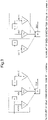
- FIG. 3 is a diagram illustrating a configuration of a skew compensation filter employing the FIR filter.
- FIG. 3 shows configurations of the skew compensation filter, in the following cases (a) the amount of skew compensation is -x sample (0 ⁇ x ⁇ 1) and (b) the amount of skew compensation is +x sample (0 ⁇ x ⁇ 1). In each case, if each tap coefficient is set appropriately, b (n) in the equation (1) can be calculated.
- FIG. 3 illustrates an example of 3-tap FIR filter. A higher degree FIR filter may be employed in order to conduct wide range skew compensation.
- sampling rate of the A/D converter 101 cannot be fully increased due to limit of operation speed and consumed power in a high-speed communication of more than 10G bps. Due to the limit, an over-sampling operation is usually conducted at one to two times a baud rate of a signal. As a result, the problem occurs that satisfactory filter characteristics are not obtained.
- FIG. 4 is a diagram illustrating propagation characteristics of the skew compensation filter.
- FIG. 4 illustrates an example of calculated propagation characteristics in performance of 64 GS/s (Giga-Sample per second) with respect to a signal with 32 Gb/s using the FIR filter shown in FIG. 3 . The example shows double over-sampling is performed.
- FIG. 4 (i) and FIG. 4 (ii) illustrate calculation results of propagation characteristics of FIR filter on the amount of skew compensation of 0.1 sample and the amount of skew compensation of 0.49 sample, respectively.
- a left axis represents amplitude characteristics (transit characteristics)
- a right axis represents group delay characteristics (amount of skew compensation).
- a frequency, at which 0.1 sample which is a desired amount of skew compensation as group delay is obtained is around 10GHz or less.
- performance of a waveform distortion compensation filter may be insufficient, because the amount of over-sample in the A/D converter 101 is insufficient.
- waveform distortion may not be fully removed (compensated) or additional waveform distortion (deterioration of propagation characteristics) may further occur.
- the digital receiver of the first exemplary embodiment of the invention further includes the band compensation filter 104 to solve the above problem.
- the digital receiver of the first exemplary embodiment compensates deterioration of band characteristics due to the skew compensation filter 103 by using the band compensation filter 104 to achieve desired signal propagation characteristics.
- a method of skew compensation and an amount of skew compensation are determined, change of propagation characteristics due to the skew compensation filter 103 is determined uniquely. Therefore, when the band compensation filter 104 having propagation characteristics of suppressing propagation characteristics deterioration due to skew compensation is employed, it is possible to compensate additional waveform distortion which occurs in skew compensation filter 103.
- a filter which does not change group delay characteristics of the skew compensation filter 103, and only amplitude characteristics of which is opposite to the characteristics of the skew compensation filter 103 may be employed as the band compensation filter 104.
- the band compensation filter 104 may be configured by using the FIR filter.
- the filter coefficient setting circuit 106 may calculate a filter coefficient by which desired characteristics opposite to characteristics of the skew compensation filter 103 is achieved in the band compensation filter 104.
- the set value of the band compensation filter 104 may be set by referring to the look-up table which is calculated in advance based on the set value of the filter coefficient setting circuit 105.
- the set value of the filter coefficient setting circuit 106 only has to be determined so that proper system performance is obtained by considering allowable circuit size and consumed power and performance required for a system, like band characteristics, group delay characteristics and the like.
- the set value of the filter coefficient setting circuit 106 may be determined so that system performance, like an error rate, is optimized.
- the skew compensation filter 103 with a linear interpolation circuit in FIG. 3 is one example of a skew compensation system, and other system is available as the skew compensation system.
- a method using a higher-order FIR filter or a method of conducting rate conversion by using up-sampling and an interpolation filter may also conduct skew compensation.
- the digital receiver 100 determines a set value of the filter coefficient setting circuit 107 by associating propagation characteristics of the skew compensation filter 103 with that of the band compensation filter and by considering circuit size and consumed power, and preferential performance (band characteristics, group delay characteristics) in the system. Thereby, a digital receiver with desired characteristics can be configured.
- the digital receiver of the first exemplary embodiment can compensates additional waveform distortion which occurs in the skew compensation filter. Accordingly, the digital receiver of the first exemplary embodiment is well controllable and achieves distortion compensation with high performance and high accuracy.
- FIG. 5 is a diagram illustrating a configuration of a digital receiver 500 of the second exemplary embodiment of the invention.
- the digital receiver 500 includes a polarization diversity 90-degree hybrid 501, an optical-electric (O/E) converter 502, an A/D converter 503, a skew compensation filter 504 and a wavelength dispersion compensation filter 505.
- O/E optical-electric
- a DP-QPSK signal light is a signal light transmitted from an optical transmitter which is not shown.
- the DP-QPSK signal light with waveform distortion due to wavelength dispersion of an optical fiber transmission path is received by the digital receiver 500 of the invention.
- the received DP-QPSK signal light is combined with a local oscillator light in the polarization diversity 90-degree hybrid 501 and is demodulated into 4 channels optical signals Ix, Qx, Iy, Qy.
- the 4 demodulated signals Ix, Qx, Iy, Qy are converted to electric signals by the O/E converters (optical electric converter) 502-1 to 502-4, respectively.
- the signals Ix, Qx, Iy, Qy, which have been converted to electric signals, are converted into digital signals by the following A/D converters 503-1 to 503-4, respectively.
- the skew compensation filter 504 compensates skew between channels of signals converted to the digital signals.
- the wavelength dispersion compensation filter 505 removes (compensates) waveform distortion which is included in the inputted signals and is caused by wavelength dispersion added in the optical transmission path. Outputs of the wavelength dispersion compensation filter 505 enter the digital signal processing circuit 508.
- the digital signal processing circuit 508 gives, to the inputted signals, digital signal processing, like clock extraction, retiming, polarization tracking, local oscillator light phase estimation, and the like. Since the detailed processes in the digital signal processing circuit 508 has no relation with the invention and is described in Non-Patent Document 1 to be publicly known, descriptions thereof is omitted.
- the skew compensation filter 504 in the digital receiver 500 of the second exemplary embodiment of the invention may be the filter conducting linear interpolation, shown in FIG. 3 , just like the digital receiver 100 of the first exemplary embodiment of the invention.
- a filter which is configured by combining butterfly-typed FIR filters compensating crosstalk between the Ix (Iy) channel and the Qx (Qy) channel, as shown in FIG. 6 may also be employed as the skew compensation filter 504.
- FIG. 7 is a diagram illustrating a configuration of the FDE (frequency domain equalization) wavelength dispersion compensation filter 505.
- the signals of I-ch and Q-ch enter a FFT (fast Fourier transform) circuit and are converted into complex frequency region signals. Weighted multiplication is performed on signals converted to the complex frequency region signals by a set value of a filter coefficient of the filter coefficient setting circuit 507 related to the wavelength dispersion compensation filter, IFFT (inverse FFT) is further performed thereon, and the signals are converted into time domain signals and outputted.
- FFT fast Fourier transform
- the filter coefficient setting circuit 507 calculates the product of the inverse function f -1 ( ⁇ ) of the function f ( ⁇ ) representing deterioration of propagation characteristic of the skew compensation filter 504 and the inverse function g -1 ( ⁇ ) of the propagation characteristics g ( ⁇ ) related to wavelength dispersion compensation, as a filter coefficient. Accordingly, it becomes possible to compensate waveform distortion added by the skew compensation filter 504 by using the wavelength dispersion compensation filter 505.
- the function f ( ⁇ ) representing deterioration of propagation characteristic of the skew compensation filter 504 is a function extracting only amplitude characteristics (an absolute value of propagation characteristics of the skew compensation filter 504) of the graph in FIG. 4 .
- the DP-QPSK signal is exemplified as an input signal.
- the invention may be applied to a signal of various modulation systems, like ASK (amplitude shift keying), BPSK (binary PSK), SP (single polarization)-QPSK, OFDM (orthogonal frequency division multiplexing) signal.
- ASK amplitude shift keying
- BPSK binary PSK
- SP single polarization
- OFDM orthogonal frequency division multiplexing
- the digital receiver of the second exemplary embodiment calculates the product of the inverse function f -1 ( ⁇ ) of the function f ( ⁇ ) representing deterioration of propagation characteristic of the skew compensation filter and the inverse function g -1 ( ⁇ ) of the propagation characteristics g ( ⁇ ) related to wavelength dispersion compensation, as a filter coefficient.
- the digital receiver of the second exemplary embodiment compensates waveform distortion added by the skew compensation filter by using the wavelength dispersion compensation filter. Accordingly, the digital receiver of the second exemplary embodiment is well controllable and achieves distortion compensation with high performance and high accuracy.
- FIG. 8 is a diagram illustrating a digital filter 800 of the third exemplary embodiment of the invention.
- the digital filter 800 includes an A/D converter 101, an A/D converter identification clock 102, a first distortion compensation filter 801 and a second distortion compensation filter 802.
- the digital filter 800 further includes a filter coefficient setting circuit 803 related to the first distortion compensation filter and a filter coefficient setting circuit 804 related to the second distortion compensation filter.
- a signal which is received by a receiver through a transmission path and is O/E-converted, enters the A/D converter 101.
- the A/D converter 101 converts the inputted signal, which is an analog electric signal, into a digital signal at the timing in synchronization with the A/D converter identification clock 102.
- the digital filter 800 of the third exemplary embodiment works to associate propagation characteristics of the first distortion compensation filter with propagation characteristics of the second distortion compensation filter. As a result, even when it is difficult for the first distortion compensation filter alone to sufficiently achieve distortion compensation, the digital filter 800 is well-controllable and achieves distortion compensation with high performance and high accuracy.
- the first distortion compensation filter 801 and the second distortion compensation filter 802 may not necessarily be separated filters in circuit implementation.
- the first distortion compensation filter 801 and the second distortion compensation filter 802 may be configured as one high-order FIR filter.
- filter coefficient calculation on the filter coefficient setting circuit 803 and filter coefficient calculation on the filter coefficient setting circuit 804 may be separated to set coefficients, based on the process equivalent to the above. Even if the first distortion compensation filter 801 and the second distortion compensation filter 802 is configured as one high-order FIR filter, controllability equivalent to that of the configuration including these filters separately is obtained by carrying out each filter coefficient calculation individually.
- the digital filter 800 without the A/D converter 101 and the A/D converter identification clock 102 may compensate distortion of an inputted signal based on processes similar to the processes described in the third exemplary embodiment.
- the digital filter 800 may be the configuration including only the first distortion compensation filter 801, the second distortion compensation filter 802, the filter coefficient setting circuit 803 related to the first distortion compensation filter and the filter coefficient setting circuit 804 related to the second distortion compensation filter.
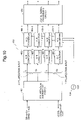
- FIG. 9 is a diagram illustrating a digital filter 900 of the modified example of the digital filter 800 related to the third exemplary embodiment of the invention.
- the digital filter 900 includes a half fixed distortion compensation filter 901, an adaptive equalization distortion compensation filter 902, a filter coefficient setting circuit 903 related to the half fixed distortion compensation filter, a filter coefficient setting circuit 904 related to the adaptive equalization filter, a digital signal processing circuit 905 and a signal quality monitor 906.
- the digital filter 900 differs from the digital filter 800 of the third exemplary embodiment of the invention in the configuration of the employed waveform distortion filter, and the other configuration thereof is similar to the configuration of the third exemplary embodiment. Therefore, the same reference numerals as those of the digital receiver 800 are given to the corresponding parts of the digital filter 900, and descriptions thereabout are omitted.
- the filter coefficient setting circuit 903 sets the filter coefficient of the half fixed distortion compensation filter 901 based on compensation amount setting information.
- the adaptive equalization distortion compensation filter 902 conducts adaptive equalization based on LMS (least mean square) algorithm or the like by using a decision feedback signal or a training signal or the like.
- the digital receiver 900 may conduct adaptive equalization based on information of the signal quality monitor 906 like an error rate, a waveform monitor, or the like.
- filter coefficient calculation of the filter coefficient setting circuit 904 is conducted based on setting information set by the filter coefficient setting circuit 903, by preliminarily considering, aside from adaptive equalization, additional fixed distortion due to the half fixed distortion compensation filter 901, convergence and controllability of adaptive equalization can be improved.
- Waveform distortion which can be compensated by the half fixed distortion compensation filter 901 is, for example, waveform distortion in the transmitter, the transmission path, and the optical front-end part (each not shown) and distortion due to calibration error on the A/D converter 101.
- the present modified example may be applied to compensation for distortion due to a band limitation filter of a duo-binary modulation system, distortion due to a conversion filter from a RZ (return-to-zero) signal to a NRZ (non-RZ) signal, and the like.
- the digital filter device of the second modified example of the third exemplary embodiment is well controllable and achieves distortion compensation with high performance and high accuracy.
- each exemplary embodiment described above may be achieved by a computer.
- the digital receiver or the digital filter device in each exemplary embodiment may include a central processing unit and memory.
- the central processing unit may achieve the function of the digital receiver or the digital filter device in each exemplary embodiment by executing a program stored in the memory.
Claims (9)
- Digitale Filtervorrichtung, mit:einer ersten Verzerrungskompensationsfiltereinrichtung (801) zum Ausführen einer Verzerrungskompensation für eine in einem Eingangssignal enthaltene erste Wellenformverzerrung durch digitale Signalverarbeitung;einer ersten Filterkoeffizienteneinstelleinrichtung (803) zum Einstellen eines Filterkoeffizienten der ersten Verzerrungskompensationsfiltereinrichtung (801);einer zweiten Verzerrungskompensationsfiltereinrichtung (802) zum Kompensieren einer zweiten Wellenformverzerrung, die in einem von der ersten Verzerrungskompensationsfiltereinrichtung (801) ausgegebenen Signal enthalten ist;einer zweiten Filterkoeffizienteneinstelleinrichtung (804) zum Einstellen eines Filterkoeffizienten der zweiten Verzerrungskompensationsfiltereinrichtung (802) basierend auf dem durch die erste Filterkoeffizienteneinstelleinrichtung (803) eingestellten Filterkoeffizienten; undeiner A/D-Wandlereinrichtung (101) zum Umwandeln eines analogen Eingangssignals in ein digitales Signal und zum Zuführen des umgewandelten digitalen Signals zur ersten Verzerrungskompensationsfiltereinrichtung (801),wobei ein Ausgangssignal der A/D-Wandlereinrichtung (101) der ersten Verzerrungskompensationsfiltereinrichtung (801) zugeführt wird.
- Digitale Filtervorrichtung nach Anspruch 1, wobei die zweite Filterkoeffizienteneinstelleinrichtung (804) den Filterkoeffizienten der zweiten Verzerrungskompensationsfiltereinrichtung (802) derart einstellt, dass eine durch den ersten Verzerrungskompensationsfilter (801) verursachte Änderung von Ausbreitungseigenschaften unterdrückt wird.
- Digitale Filtervorrichtung nach Anspruch 1, wobei die zweite Filterkoeffizienteneinstelleinrichtung (804) den Filterkoeffizienten der zweiten Verzerrungskompensationsfiltereinrichtung (802) derart einstellt, dass eine durch die erste Verzerrungskompensationsfiltereinrichtung (801) verursachte Änderung der Amplitudeneigenschaften unterdrückt wird.
- Digitale Filtervorrichtung nach einem der Ansprüche 1 bis 3, wobei die erste Verzerrungskompensationsfiltereinrichtung (801) eine Verzögerungskompensationseinrichtung (103) zum Kompensieren einer Verzögerung eines Eingangssignals ist.
- Digitale Filtervorrichtung nach Anspruch 4, wobei die Verzögerungskompensationseinrichtung (103) ein FIR-, Finite Impulse Response, Filter aufweist, und wobei die erste Filterkoeffizienteneinstelleinrichtung (803) einen Filterkoeffizienten des FIR-Filters in Antwort auf vorgegebene Verzögerungskompensationscharakteristiken berechnet.
- Digitale Filtervorrichtung nach einem der Ansprüche 1 bis 5, wobei die zweite Verzerrungskompensationsfiltereinrichtung (802) eine Frequenzbereich-Entzerrungsschaltung (505) aufweist.
- Digitale Filtervorrichtung nach einem der Ansprüche 1 bis 6, ferner mit:einer Digitalsignalverarbeitungseinrichtung (905) zum digitalen Verarbeiten eines von der zweiten Verzerrungskompensationsfiltereinrichtung (802) ausgegebenen Signals; undeiner Signalqualitätsüberwachungseinrichtung (906) zum Überwachen einer Qualität eines von der Digitalsignalverarbeitungseinrichtung (905) ausgegebenen Signals, wobei die zweite Filterkoeffizienteneinstelleinrichtung (804) den Filterkoeffizienten der zweiten Verzerrungskompensationsfiltereinrichtung (802) basierend auf einem Überwachungsergebnis der Signalqualitätsüberwachungseinrichtung bestimmt.
- Digitales Filterverfahren, mit den Schritten:Einstellen eines Filterkoeffizienten einer ersten Verzerrungskompensationsfiltereinrichtung (801);Kompensieren einer Verzerrung einer ersten Wellenformverzerrung, die in einem Eingangssignal enthalten ist;Einstellen eines Filterkoeffizienten einer zweiten Verzerrungskompensationsfiltereinrichtung (802) basierend auf dem Filterkoeffizienten der ersten Verzerrungskompensationsfiltereinrichtung (801);Kompensieren einer zweiten Wellenformverzerrung, die in einem von der ersten Verzerrungskompensationsfiltereinrichtung (801) ausgegebenen Signal enthalten ist; undUmwandeln eines analogen Eingangssignals in ein digitales Signal durch eine A/D-Wandlereinrichtung (101) und Zuführen des umgewandelten digitalen Signals zur ersten Verzerrungskompensationsfiltereinrichtung (801),wobei ein Ausgangssignal der A/D-Wandlereinrichtung (101) der ersten Verzerrungskompensationsfiltereinrichtung (801) zugeführt wird.
- Steuerprogramm einer digitalen Filtervorrichtung, das einen Computer der digitalen Filtervorrichtung veranlasst, zu funktionieren als:eine erste Verzerrungskompensationsfiltereinrichtung (801) zum Ausführen einer Verzerrungskompensation einer in einem Eingangssignal enthaltenen ersten Wellenformverzerrung durch digitale Signalverarbeitung;eine erste Filterkoeffizienteneinstelleinrichtung (803) zum Einstellen eines Filterkoeffizienten der ersten Verzerrungskompensationsfiltereinrichtung (801);eine zweite Verzerrungskompensationsfiltereinrichtung (802) zum Kompensieren einer zweiten Wellenformverzerrung, die in einem von der ersten Verzerrungskompensationsfiltereinrichtung (801) ausgegebenen Signal enthalten ist;eine zweite Filterkoeffizienteneinstelleinrichtung (804) zum Einstellen eines Filterkoeffizienten der zweiten Verzerrungskompensationsfiltereinrichtung (802) basierend auf dem durch die erste Filterkoeffizienteneinstelleinrichtung (803) eingestellten Filterkoeffizienten; undeine A/D-Wandlereinrichtung (101) zum Umwandeln eines analogen Eingangssignals in ein digitales Signal und zum Zuführen des umgewandelten digitalen Signals zur ersten Verzerrungskompensationsfiltereinrichtung (801),wobei ein Ausgangssignal der A/D-Wandlereinrichtung (101) der ersten Verzerrungskompensationsfiltereinrichtung (801) zugeführt wird.
Applications Claiming Priority (2)
| Application Number | Priority Date | Filing Date | Title |
|---|---|---|---|
| JP2010195370 | 2010-09-01 | ||
| PCT/JP2011/069103 WO2012029613A1 (ja) | 2010-09-01 | 2011-08-18 | デジタルフィルタ装置、デジタルフィルタリング方法及びデジタルフィルタ装置の制御プログラム |
Publications (3)
| Publication Number | Publication Date |
|---|---|
| EP2613452A1 EP2613452A1 (de) | 2013-07-10 |
| EP2613452A4 EP2613452A4 (de) | 2016-12-21 |
| EP2613452B1 true EP2613452B1 (de) | 2022-12-28 |
Family
ID=45772705
Family Applications (1)
| Application Number | Title | Priority Date | Filing Date |
|---|---|---|---|
| EP11821630.8A Active EP2613452B1 (de) | 2010-09-01 | 2011-08-18 | Digitale filtervorrichtung, digitales filterverfahren und steuerprogramm für die digitale filtervorrichtung |
Country Status (5)
| Country | Link |
|---|---|
| US (1) | US8831081B2 (de) |
| EP (1) | EP2613452B1 (de) |
| JP (1) | JP4968415B2 (de) |
| CN (1) | CN103004098B (de) |
| WO (1) | WO2012029613A1 (de) |
Families Citing this family (17)
| Publication number | Priority date | Publication date | Assignee | Title |
|---|---|---|---|---|
| US9686019B2 (en) * | 2010-12-21 | 2017-06-20 | Nec Corporation | Coherent optical receiver, device and method for detecting inter-lane skew in coherent optical receiver |
| CN102655433B (zh) * | 2011-03-04 | 2016-03-30 | 富士通株式会社 | 非线性损伤补偿方法和装置 |
| WO2013084391A1 (ja) * | 2011-12-08 | 2013-06-13 | 日本電気株式会社 | デジタル受信機及び波形補償方法 |
| CN103856426B (zh) * | 2012-12-03 | 2017-04-19 | 华为技术有限公司 | 一种补偿滤波器的实现方法及信号带宽补偿的装置 |
| US9240843B1 (en) * | 2012-12-28 | 2016-01-19 | Juniper Networks, Inc. | Method and apparatus for blind time skew compensation for coherent optical receivers |
| JP5856580B2 (ja) * | 2013-03-14 | 2016-02-10 | 日本電信電話株式会社 | 信号処理装置、及び信号処理方法 |
| JP6500781B2 (ja) * | 2013-12-09 | 2019-04-17 | 日本電気株式会社 | 等化処理回路、デジタル受信機、信号送受信システム、等化処理方法およびデジタル受信方法 |
| EP3132548B1 (de) * | 2014-04-15 | 2021-06-02 | ARRIS Enterprises LLC | Intelligente empfänger und sender für kabelfernsehnetzwerke |
| US9912414B2 (en) * | 2014-11-14 | 2018-03-06 | Zte Corporation | Iterative post-equalization for coherent optical receivers |
| JP6759742B2 (ja) * | 2016-06-16 | 2020-09-23 | 富士通株式会社 | 受信装置及び設定方法 |
| JP6206545B1 (ja) * | 2016-06-17 | 2017-10-04 | Nttエレクトロニクス株式会社 | 伝送特性補償装置、伝送特性補償方法及び通信装置 |
| CN106100751B (zh) * | 2016-07-29 | 2018-08-07 | 上海南明光纤技术有限公司 | 用于高速光脉冲幅度调制的改进的维纳滤波方法及系统 |
| JP7007588B2 (ja) * | 2018-06-18 | 2022-01-24 | 日本電信電話株式会社 | 信号処理装置及び光受信装置 |
| JP6610742B1 (ja) * | 2018-10-09 | 2019-11-27 | Nttエレクトロニクス株式会社 | 適応等化装置、適応等化方法及び通信装置 |
| CN111585646B (zh) * | 2019-02-19 | 2023-03-31 | 富士通株式会社 | 偏振态相对时延的估计装置以及方法 |
| US11323184B2 (en) * | 2019-11-29 | 2022-05-03 | Maxim Integrated Products, Inc. | Chromatic dispersion equalizer adaption systems and methods |
| CA3189536A1 (en) * | 2020-08-18 | 2022-02-24 | David L. Hershberger | Loran transmitter, receiver, system and method of operating same |
Family Cites Families (30)
| Publication number | Priority date | Publication date | Assignee | Title |
|---|---|---|---|---|
| JPS57183139A (en) * | 1981-05-07 | 1982-11-11 | Nec Corp | Automatic amplitude equalizing circuit |
| JPS5833313A (ja) * | 1981-08-21 | 1983-02-26 | Nec Corp | トランスバ−サル定利得可変等化器 |
| JPS62104211A (ja) * | 1985-10-30 | 1987-05-14 | Fujitsu Ltd | 回線等化方式 |
| JPH02235442A (ja) * | 1989-03-09 | 1990-09-18 | Nec Corp | データ変復調装置の自動等化方式 |
| US5157395A (en) * | 1991-03-04 | 1992-10-20 | Crystal Semiconductor Corporation | Variable decimation architecture for a delta-sigma analog-to-digital converter |
| JPH04362808A (ja) | 1991-06-11 | 1992-12-15 | Hitachi Ltd | 等化回路 |
| JPH05130452A (ja) * | 1991-10-31 | 1993-05-25 | Hitachi Ltd | 可変フイルタ装置 |
| FI95086C (fi) * | 1992-11-26 | 1995-12-11 | Nokia Mobile Phones Ltd | Menetelmä puhesignaalin tehokkaaksi koodaamiseksi |
| JP2872547B2 (ja) * | 1993-10-13 | 1999-03-17 | シャープ株式会社 | 格子型フィルタを用いた能動制御方法および装置 |
| US5864798A (en) * | 1995-09-18 | 1999-01-26 | Kabushiki Kaisha Toshiba | Method and apparatus for adjusting a spectrum shape of a speech signal |
| US5815496A (en) * | 1995-09-29 | 1998-09-29 | Lucent Technologies Inc. | Cascade echo canceler arrangement |
| US6987812B1 (en) | 1998-09-28 | 2006-01-17 | Infineon Technologies Ag | Digital receiver for a signal generated with discrete multi-tone modulation |
| KR100307662B1 (ko) * | 1998-10-13 | 2001-12-01 | 윤종용 | 가변적인수행속도를지원하는에코제거장치및방법 |
| GB2344263B (en) * | 1998-11-28 | 2003-07-02 | Matra Marconi Space Uk Ltd | Digital signal processing apparatus |
| JP3677188B2 (ja) * | 2000-02-17 | 2005-07-27 | セイコーエプソン株式会社 | 画像表示装置および方法、並びに、画像処理装置および方法 |
| US7099822B2 (en) * | 2002-12-10 | 2006-08-29 | Liberato Technologies, Inc. | System and method for noise reduction having first and second adaptive filters responsive to a stored vector |
| JP2005151011A (ja) * | 2003-11-13 | 2005-06-09 | Renesas Technology Corp | 高周波信号受信装置および半導体集積回路 |
| US7613260B2 (en) * | 2005-11-21 | 2009-11-03 | Provigent Ltd | Modem control using cross-polarization interference estimation |
| JP2007294011A (ja) * | 2006-04-25 | 2007-11-08 | Hitachi Global Storage Technologies Netherlands Bv | ディスク・ドライブ装置 |
| JP2008048104A (ja) * | 2006-08-14 | 2008-02-28 | Sony Corp | 撮像装置と欠陥補正回路および欠陥補正方法 |
| JP4764814B2 (ja) * | 2006-12-28 | 2011-09-07 | 株式会社日立製作所 | 波形等化係数調整方法および回路、レシーバ回路、ならびに伝送装置 |
| JP4303760B2 (ja) | 2007-02-16 | 2009-07-29 | 富士通株式会社 | Ad変換制御装置、光受信装置および光受信方法 |
| US7912119B2 (en) * | 2007-08-23 | 2011-03-22 | Freescale Semiconductor, Inc. | Per-survivor based adaptive equalizer |
| KR20090051622A (ko) * | 2007-11-19 | 2009-05-22 | 삼성전자주식회사 | 데이터 재생 장치 및 방법 |
| JP5157479B2 (ja) * | 2008-01-28 | 2013-03-06 | 富士通株式会社 | 歪補償装置及びこれを備えた電力増幅装置 |
| JP5136236B2 (ja) * | 2008-06-19 | 2013-02-06 | 富士通株式会社 | 光受信装置 |
| JP5217792B2 (ja) * | 2008-08-29 | 2013-06-19 | 富士通株式会社 | 光受信機の電力供給制御方法、並びに、デジタル信号処理回路および光受信機 |
| CN101753217B (zh) * | 2008-11-28 | 2012-11-21 | 富士通株式会社 | 色散监控装置和方法、色散补偿装置 |
| JP5407403B2 (ja) * | 2009-02-18 | 2014-02-05 | 富士通株式会社 | 信号処理装置および光受信装置 |
| US8199924B2 (en) * | 2009-04-17 | 2012-06-12 | Harman International Industries, Incorporated | System for active noise control with an infinite impulse response filter |
-
2011
- 2011-08-18 EP EP11821630.8A patent/EP2613452B1/de active Active
- 2011-08-18 JP JP2011552647A patent/JP4968415B2/ja active Active
- 2011-08-18 CN CN201180035195.8A patent/CN103004098B/zh active Active
- 2011-08-18 US US13/393,066 patent/US8831081B2/en active Active
- 2011-08-18 WO PCT/JP2011/069103 patent/WO2012029613A1/ja active Application Filing
Also Published As
| Publication number | Publication date |
|---|---|
| EP2613452A1 (de) | 2013-07-10 |
| JP4968415B2 (ja) | 2012-07-04 |
| CN103004098B (zh) | 2014-09-03 |
| WO2012029613A1 (ja) | 2012-03-08 |
| EP2613452A4 (de) | 2016-12-21 |
| US20130287390A1 (en) | 2013-10-31 |
| JPWO2012029613A1 (ja) | 2013-10-28 |
| US8831081B2 (en) | 2014-09-09 |
| CN103004098A (zh) | 2013-03-27 |
Similar Documents
| Publication | Publication Date | Title |
|---|---|---|
| EP2613452B1 (de) | Digitale filtervorrichtung, digitales filterverfahren und steuerprogramm für die digitale filtervorrichtung | |
| CA3047882C (en) | Optical transmission characteristic estimation method, optical transmission characteristic compensation method, optical transmission characteristic estimation system and optical transmission characteristic compensation system | |
| CN109314572B (zh) | 传输特性补偿装置、传输特性补偿方法以及通信装置 | |
| US8707138B2 (en) | Method and arrangement for blind demultiplexing a polarisation diversity multiplex signal | |
| EP2399353B1 (de) | Entzerrer für ein optisches übertragungssystem | |
| US20100196009A1 (en) | Polarization independent frequency domain equalization (fde) for chromatic dispersion (cd) compensation in polmux coherent systems | |
| US8750442B2 (en) | Digital receiver and waveform compensation method | |
| Cheng et al. | A low-complexity adaptive equalizer for digital coherent short-reach optical transmission systems | |
| US10985845B2 (en) | Adaptive equalization filter and signal processing device | |
| JP2016025518A (ja) | 光受信器、送受信装置、光通信システムおよび波形歪補償方法 | |
| Pan et al. | Fractionally-spaced frequency domain linear crosstalk cancellation with spectral alignment techniques for coherent superchannel optical systems | |
| Hamja et al. | DSP aided chromatic dispersion reckoning in single carrier high speed coherent optical communications | |
| WO2023067641A1 (ja) | デジタル信号処理回路、方法、受信機、及び通信システム | |
| WO2023073927A1 (ja) | デジタル信号処理回路、方法、受信機、及び通信システム | |
| EP2362557B1 (de) | MLSE bei kohärentem optischen Empfänger für optische Filtertoleranz | |
| EP2271006A1 (de) | System und Verfahren zur elektronischen Dispersionskompensation | |
| EP3133751A1 (de) | Verfahren zur nichtlinearitätskompensierung in optischen übertragungssystemen | |
| Hauske et al. | Reduced complexity Rx concepts for optical multilevel transmission | |
| Pinto et al. | Real-time digital signal processing for coherent optical systems | |
| Panhwar et al. | Reduced sampling rate frequency domain CD equalization for 112 Gb/s PDM-QPSK | |
| EP2446562A2 (de) | System und verfahren für elektronische dispersionskompensation | |
| Blow et al. | 40Gb/s Distortion Mitigation and DSP-Based Equalisat |
Legal Events
| Date | Code | Title | Description |
|---|---|---|---|
| PUAI | Public reference made under article 153(3) epc to a published international application that has entered the european phase |
Free format text: ORIGINAL CODE: 0009012 |
|
| 17P | Request for examination filed |
Effective date: 20130206 |
|
| AK | Designated contracting states |
Kind code of ref document: A1 Designated state(s): AL AT BE BG CH CY CZ DE DK EE ES FI FR GB GR HR HU IE IS IT LI LT LU LV MC MK MT NL NO PL PT RO RS SE SI SK SM TR |
|
| DAX | Request for extension of the european patent (deleted) | ||
| RA4 | Supplementary search report drawn up and despatched (corrected) |
Effective date: 20161121 |
|
| RIC1 | Information provided on ipc code assigned before grant |
Ipc: H04L 27/00 20060101ALI20161115BHEP Ipc: H03H 17/02 20060101ALI20161115BHEP Ipc: H04B 3/04 20060101AFI20161115BHEP |
|
| STAA | Information on the status of an ep patent application or granted ep patent |
Free format text: STATUS: EXAMINATION IS IN PROGRESS |
|
| STAA | Information on the status of an ep patent application or granted ep patent |
Free format text: STATUS: EXAMINATION IS IN PROGRESS |
|
| 17Q | First examination report despatched |
Effective date: 20210112 |
|
| STAA | Information on the status of an ep patent application or granted ep patent |
Free format text: STATUS: EXAMINATION IS IN PROGRESS |
|
| GRAP | Despatch of communication of intention to grant a patent |
Free format text: ORIGINAL CODE: EPIDOSNIGR1 |
|
| STAA | Information on the status of an ep patent application or granted ep patent |
Free format text: STATUS: GRANT OF PATENT IS INTENDED |
|
| INTG | Intention to grant announced |
Effective date: 20220727 |
|
| GRAS | Grant fee paid |
Free format text: ORIGINAL CODE: EPIDOSNIGR3 |
|
| GRAA | (expected) grant |
Free format text: ORIGINAL CODE: 0009210 |
|
| STAA | Information on the status of an ep patent application or granted ep patent |
Free format text: STATUS: THE PATENT HAS BEEN GRANTED |
|
| AK | Designated contracting states |
Kind code of ref document: B1 Designated state(s): AL AT BE BG CH CY CZ DE DK EE ES FI FR GB GR HR HU IE IS IT LI LT LU LV MC MK MT NL NO PL PT RO RS SE SI SK SM TR |
|
| REG | Reference to a national code |
Ref country code: GB Ref legal event code: FG4D |
|
| REG | Reference to a national code |
Ref country code: CH Ref legal event code: EP |
|
| REG | Reference to a national code |
Ref country code: DE Ref legal event code: R096 Ref document number: 602011073562 Country of ref document: DE |
|
| REG | Reference to a national code |
Ref country code: AT Ref legal event code: REF Ref document number: 1541116 Country of ref document: AT Kind code of ref document: T Effective date: 20230115 |
|
| REG | Reference to a national code |
Ref country code: IE Ref legal event code: FG4D |
|
| REG | Reference to a national code |
Ref country code: LT Ref legal event code: MG9D |
|
| PG25 | Lapsed in a contracting state [announced via postgrant information from national office to epo] |
Ref country code: SE Free format text: LAPSE BECAUSE OF FAILURE TO SUBMIT A TRANSLATION OF THE DESCRIPTION OR TO PAY THE FEE WITHIN THE PRESCRIBED TIME-LIMIT Effective date: 20221228 Ref country code: NO Free format text: LAPSE BECAUSE OF FAILURE TO SUBMIT A TRANSLATION OF THE DESCRIPTION OR TO PAY THE FEE WITHIN THE PRESCRIBED TIME-LIMIT Effective date: 20230328 Ref country code: LT Free format text: LAPSE BECAUSE OF FAILURE TO SUBMIT A TRANSLATION OF THE DESCRIPTION OR TO PAY THE FEE WITHIN THE PRESCRIBED TIME-LIMIT Effective date: 20221228 Ref country code: FI Free format text: LAPSE BECAUSE OF FAILURE TO SUBMIT A TRANSLATION OF THE DESCRIPTION OR TO PAY THE FEE WITHIN THE PRESCRIBED TIME-LIMIT Effective date: 20221228 |
|
| REG | Reference to a national code |
Ref country code: NL Ref legal event code: MP Effective date: 20221228 |
|
| REG | Reference to a national code |
Ref country code: AT Ref legal event code: MK05 Ref document number: 1541116 Country of ref document: AT Kind code of ref document: T Effective date: 20221228 |
|
| PG25 | Lapsed in a contracting state [announced via postgrant information from national office to epo] |
Ref country code: RS Free format text: LAPSE BECAUSE OF FAILURE TO SUBMIT A TRANSLATION OF THE DESCRIPTION OR TO PAY THE FEE WITHIN THE PRESCRIBED TIME-LIMIT Effective date: 20221228 Ref country code: LV Free format text: LAPSE BECAUSE OF FAILURE TO SUBMIT A TRANSLATION OF THE DESCRIPTION OR TO PAY THE FEE WITHIN THE PRESCRIBED TIME-LIMIT Effective date: 20221228 Ref country code: HR Free format text: LAPSE BECAUSE OF FAILURE TO SUBMIT A TRANSLATION OF THE DESCRIPTION OR TO PAY THE FEE WITHIN THE PRESCRIBED TIME-LIMIT Effective date: 20221228 Ref country code: GR Free format text: LAPSE BECAUSE OF FAILURE TO SUBMIT A TRANSLATION OF THE DESCRIPTION OR TO PAY THE FEE WITHIN THE PRESCRIBED TIME-LIMIT Effective date: 20230329 |
|
| PG25 | Lapsed in a contracting state [announced via postgrant information from national office to epo] |
Ref country code: NL Free format text: LAPSE BECAUSE OF FAILURE TO SUBMIT A TRANSLATION OF THE DESCRIPTION OR TO PAY THE FEE WITHIN THE PRESCRIBED TIME-LIMIT Effective date: 20221228 |
|
| PG25 | Lapsed in a contracting state [announced via postgrant information from national office to epo] |
Ref country code: SM Free format text: LAPSE BECAUSE OF FAILURE TO SUBMIT A TRANSLATION OF THE DESCRIPTION OR TO PAY THE FEE WITHIN THE PRESCRIBED TIME-LIMIT Effective date: 20221228 Ref country code: RO Free format text: LAPSE BECAUSE OF FAILURE TO SUBMIT A TRANSLATION OF THE DESCRIPTION OR TO PAY THE FEE WITHIN THE PRESCRIBED TIME-LIMIT Effective date: 20221228 Ref country code: PT Free format text: LAPSE BECAUSE OF FAILURE TO SUBMIT A TRANSLATION OF THE DESCRIPTION OR TO PAY THE FEE WITHIN THE PRESCRIBED TIME-LIMIT Effective date: 20230428 Ref country code: ES Free format text: LAPSE BECAUSE OF FAILURE TO SUBMIT A TRANSLATION OF THE DESCRIPTION OR TO PAY THE FEE WITHIN THE PRESCRIBED TIME-LIMIT Effective date: 20221228 Ref country code: EE Free format text: LAPSE BECAUSE OF FAILURE TO SUBMIT A TRANSLATION OF THE DESCRIPTION OR TO PAY THE FEE WITHIN THE PRESCRIBED TIME-LIMIT Effective date: 20221228 Ref country code: CZ Free format text: LAPSE BECAUSE OF FAILURE TO SUBMIT A TRANSLATION OF THE DESCRIPTION OR TO PAY THE FEE WITHIN THE PRESCRIBED TIME-LIMIT Effective date: 20221228 Ref country code: AT Free format text: LAPSE BECAUSE OF FAILURE TO SUBMIT A TRANSLATION OF THE DESCRIPTION OR TO PAY THE FEE WITHIN THE PRESCRIBED TIME-LIMIT Effective date: 20221228 |
|
| PG25 | Lapsed in a contracting state [announced via postgrant information from national office to epo] |
Ref country code: SK Free format text: LAPSE BECAUSE OF FAILURE TO SUBMIT A TRANSLATION OF THE DESCRIPTION OR TO PAY THE FEE WITHIN THE PRESCRIBED TIME-LIMIT Effective date: 20221228 Ref country code: PL Free format text: LAPSE BECAUSE OF FAILURE TO SUBMIT A TRANSLATION OF THE DESCRIPTION OR TO PAY THE FEE WITHIN THE PRESCRIBED TIME-LIMIT Effective date: 20221228 Ref country code: IS Free format text: LAPSE BECAUSE OF FAILURE TO SUBMIT A TRANSLATION OF THE DESCRIPTION OR TO PAY THE FEE WITHIN THE PRESCRIBED TIME-LIMIT Effective date: 20230428 Ref country code: AL Free format text: LAPSE BECAUSE OF FAILURE TO SUBMIT A TRANSLATION OF THE DESCRIPTION OR TO PAY THE FEE WITHIN THE PRESCRIBED TIME-LIMIT Effective date: 20221228 |
|
| REG | Reference to a national code |
Ref country code: DE Ref legal event code: R097 Ref document number: 602011073562 Country of ref document: DE |
|
| PG25 | Lapsed in a contracting state [announced via postgrant information from national office to epo] |
Ref country code: DK Free format text: LAPSE BECAUSE OF FAILURE TO SUBMIT A TRANSLATION OF THE DESCRIPTION OR TO PAY THE FEE WITHIN THE PRESCRIBED TIME-LIMIT Effective date: 20221228 |
|
| PGFP | Annual fee paid to national office [announced via postgrant information from national office to epo] |
Ref country code: GB Payment date: 20230822 Year of fee payment: 13 |
|
| PLBE | No opposition filed within time limit |
Free format text: ORIGINAL CODE: 0009261 |
|
| STAA | Information on the status of an ep patent application or granted ep patent |
Free format text: STATUS: NO OPPOSITION FILED WITHIN TIME LIMIT |
|
| PGFP | Annual fee paid to national office [announced via postgrant information from national office to epo] |
Ref country code: FR Payment date: 20230824 Year of fee payment: 13 Ref country code: DE Payment date: 20230821 Year of fee payment: 13 |
|
| 26N | No opposition filed |
Effective date: 20230929 |
|
| PG25 | Lapsed in a contracting state [announced via postgrant information from national office to epo] |
Ref country code: SI Free format text: LAPSE BECAUSE OF FAILURE TO SUBMIT A TRANSLATION OF THE DESCRIPTION OR TO PAY THE FEE WITHIN THE PRESCRIBED TIME-LIMIT Effective date: 20221228 |
|
| PG25 | Lapsed in a contracting state [announced via postgrant information from national office to epo] |
Ref country code: MC Free format text: LAPSE BECAUSE OF FAILURE TO SUBMIT A TRANSLATION OF THE DESCRIPTION OR TO PAY THE FEE WITHIN THE PRESCRIBED TIME-LIMIT Effective date: 20221228 |
|
| REG | Reference to a national code |
Ref country code: CH Ref legal event code: PL |
|
| PG25 | Lapsed in a contracting state [announced via postgrant information from national office to epo] |
Ref country code: MC Free format text: LAPSE BECAUSE OF FAILURE TO SUBMIT A TRANSLATION OF THE DESCRIPTION OR TO PAY THE FEE WITHIN THE PRESCRIBED TIME-LIMIT Effective date: 20221228 |
|
| PG25 | Lapsed in a contracting state [announced via postgrant information from national office to epo] |
Ref country code: LU Free format text: LAPSE BECAUSE OF NON-PAYMENT OF DUE FEES Effective date: 20230818 |