EP2608288B1 - Organische lichtemittierende Anzeigevorrichtung und Herstellungsverfahren dafür - Google Patents
Organische lichtemittierende Anzeigevorrichtung und Herstellungsverfahren dafür Download PDFInfo
- Publication number
- EP2608288B1 EP2608288B1 EP12184787.5A EP12184787A EP2608288B1 EP 2608288 B1 EP2608288 B1 EP 2608288B1 EP 12184787 A EP12184787 A EP 12184787A EP 2608288 B1 EP2608288 B1 EP 2608288B1
- Authority
- EP
- European Patent Office
- Prior art keywords
- encapsulating layer
- layer
- inorganic
- organic
- electrode
- Prior art date
- Legal status (The legal status is an assumption and is not a legal conclusion. Google has not performed a legal analysis and makes no representation as to the accuracy of the status listed.)
- Active
Links
Images



Classifications
-
- H—ELECTRICITY
- H10—SEMICONDUCTOR DEVICES; ELECTRIC SOLID-STATE DEVICES NOT OTHERWISE PROVIDED FOR
- H10K—ORGANIC ELECTRIC SOLID-STATE DEVICES
- H10K59/00—Integrated devices, or assemblies of multiple devices, comprising at least one organic light-emitting element covered by group H10K50/00
- H10K59/80—Constructional details
- H10K59/87—Passivation; Containers; Encapsulations
- H10K59/873—Encapsulations
-
- H—ELECTRICITY
- H10—SEMICONDUCTOR DEVICES; ELECTRIC SOLID-STATE DEVICES NOT OTHERWISE PROVIDED FOR
- H10K—ORGANIC ELECTRIC SOLID-STATE DEVICES
- H10K50/00—Organic light-emitting devices
- H10K50/80—Constructional details
- H10K50/84—Passivation; Containers; Encapsulations
- H10K50/844—Encapsulations
-
- H—ELECTRICITY
- H10—SEMICONDUCTOR DEVICES; ELECTRIC SOLID-STATE DEVICES NOT OTHERWISE PROVIDED FOR
- H10K—ORGANIC ELECTRIC SOLID-STATE DEVICES
- H10K50/00—Organic light-emitting devices
- H10K50/80—Constructional details
- H10K50/84—Passivation; Containers; Encapsulations
- H10K50/844—Encapsulations
- H10K50/8445—Encapsulations multilayered coatings having a repetitive structure, e.g. having multiple organic-inorganic bilayers
-
- H—ELECTRICITY
- H10—SEMICONDUCTOR DEVICES; ELECTRIC SOLID-STATE DEVICES NOT OTHERWISE PROVIDED FOR
- H10K—ORGANIC ELECTRIC SOLID-STATE DEVICES
- H10K59/00—Integrated devices, or assemblies of multiple devices, comprising at least one organic light-emitting element covered by group H10K50/00
- H10K59/80—Constructional details
- H10K59/87—Passivation; Containers; Encapsulations
- H10K59/873—Encapsulations
- H10K59/8731—Encapsulations multilayered coatings having a repetitive structure, e.g. having multiple organic-inorganic bilayers
-
- H—ELECTRICITY
- H10—SEMICONDUCTOR DEVICES; ELECTRIC SOLID-STATE DEVICES NOT OTHERWISE PROVIDED FOR
- H10K—ORGANIC ELECTRIC SOLID-STATE DEVICES
- H10K71/00—Manufacture or treatment specially adapted for the organic devices covered by this subclass
Definitions
- the invention relates to an organic light-emitting display apparatus and a method of manufacturing the same.
- organic light-emitting display apparatuses which are self-emissive display devices, are considered as the next-generation display devices because of their wide viewing angle, high contrast ratio, and high response speed. Displays are disclosed e.g. in US 2011/284898 A1 , WO 2008/142645 A1 , US 2008/211399 A1 and US 2009/0021157 A1 .
- the invention provides an organic light-emitting display apparatus according to claim 1 and method of manufacturing an organic light-emitting display apparatus according to claim 14.
- the organic light-emitting display apparatus includes a substrate, a first electrode on the substrate, an intermediate layer on the first electrode, the intermediate layer including an organic light-emitting layer, a second electrode on the intermediate layer, a first inorganic encapsulating layer on the second electrode, the first inorganic encapsulating layer defining a first groove, a first organic encapsulating layer in the first groove defined by the first inorganic encapsulating layer, the first organic encapsulating layer not extending beyond the first groove, and a second inorganic encapsulating layer on the first organic encapsulating layer.
- the intermediate layer may include an intermediate layer protrusion.
- the second electrode may be spaced apart from the intermediate layer protrusion so as not to cover the intermediate layer protrusion.
- the first inorganic encapsulating layer may be spaced apart from the intermediate layer protrusion so as not to cover the intermediate layer protrusion.
- the organic light-emitting display apparatus may comprise a plurality of subpixels.
- a plurality of the intermediate layers may be provided to correspond to the plurality of subpixels.
- the intermediate layer protrusion may be on at least one edge of each of the plurality of intermediate layers.
- the first inorganic encapsulating layer may comprise a first inorganic protrusion that corresponds to the intermediate layer protrusion.
- the first inorganic protrusion may be disposed around the first groove.
- the first organic encapsulating layer may be spaced apart from an uppermost portion of the first inorganic protrusion.
- the first organic encapsulating layer may be spaced apart from the intermediate layer protrusion. At least one portion of the intermediate layer protrusion may contact the second inorganic encapsulating layer.
- the organic light-emitting display apparatus may further include a pixel defining film disposed on the first electrode so as not to cover a portion of a top surface of the first electrode.
- the intermediate layer protrusion may be disposed to correspond to the pixel defining film.
- the first inorganic encapsulating layer and the second inorganic encapsulating layer may contact each other at at least one portion of the first inorganic encapsulating layer.
- the second inorganic encapsulating layer may define a second groove.
- the organic light-emitting display apparatus may further include a second organic encapsulating layer disposed in the second groove of the second inorganic encapsulating layer so as not to extend beyond the second groove and a third inorganic encapsulating layer on the second organic encapsulating layer.
- the second inorganic encapsulating layer may comprise a second inorganic protrusion disposed around the second groove.
- the second organic encapsulating layer may be spaced apart from an uppermost portion of the second inorganic protrusion.
- the second organic encapsulating layer may be spaced apart from the intermediate layer protrusion.
- the second inorganic encapsulating layer and the third inorganic encapsulating layer may contact each other at at least one portion of the second inorganic encapsulating layer.
- the organic light-emitting display apparatus may further include at least one additional organic encapsulating layer and at least one additional inorganic encapsulating layer on the third inorganic encapsulating layer.
- a top surface of an uppermost organic encapsulating layer from among the at least one additional organic encapsulating layer formed on the third inorganic encapsulating layer may be flat.
- a top surface of an uppermost inorganic encapsulating layer from among the at least one additional inorganic encapsulating layer formed on the third inorganic encapsulating layer may be flat.
- a method of manufacturing an organic light-emitting display apparatus including forming a first electrode on a substrate, forming on the first electrode an intermediate layer, the intermediate layer comprising an organic light-emitting layer on the first electrode, forming a second electrode on the intermediate layer, forming a first inorganic encapsulating layer on the second electrode, the first inorganic encapsulating layer defining a first groove, forming a first organic encapsulating layer in the first groove defined by the first inorganic encapsulating layer such that the first organic encapsulating layer does not to extend beyond the first groove, and forming a second inorganic encapsulating layer on the first organic encapsulating layer.
- the intermediate layer may be formed by an imaging process.
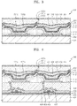
- FIG. 1 is a cross-sectional view illustrating an organic light-emitting display apparatus 100 according to an embodiment of the invention.
- the organic light-emitting display apparatus 100 comprises a substrate 101, a first electrode 110, an intermediate layer 112, a second electrode 113, a first inorganic encapsulating layer 121, a first organic encapsulating layer 131, and a second inorganic encapsulating layer 122.
- the substrate 101 may be formed of a transparent glass material having SiO 2 as a main component.
- the substrate 101 may be formed of a transparent plastic material.
- the transparent plastic material of the substrate 101 may be at least one selected from various organic materials.
- a buffer layer 102 may be formed on the substrate 101.
- the buffer layer 102 which may prevent impurity elements from penetrating through the substrate 101 and which planarizes the substrate 101, may be formed of any of various materials according to desired functions.
- the buffer layer 102 may be formed of an inorganic material such as silicon oxide, silicon nitride, silicon oxynitride, aluminum oxide, aluminum nitride, titanium oxide, or titanium nitride, an organic material such as polyimide, polyester, or acryl, or a stack of the above materials.
- the buffer layer 102 may be omitted if desired.
- the first electrode 110 may be formed on the buffer layer 102.
- the first electrode 110 may function as an anode and the second electrode 113 may function as a cathode, or vice versa.
- the first electrode 110 may include indium tin oxide (ITO), indium zinc oxide (IZO) zinc oxide (ZnO), or In 2 O 3 having a high work function.
- the first electrode 110 may further include a reflective film formed of silver (Ag), magnesium (Mg), aluminum (Al), platinum (Pt), palladium (Pd), gold (Au), nickel (Ni), neodymium (Nd), iridium (Ir), chromium (Cr), lithium (Li), ytterbium (Yb), or calcium (Ca).
- a pixel defining film 119 may be formed on the first electrode 110 by using an insulating material.
- the pixel defining film 119 may be formed to expose at least a portion of a top surface of the first electrode 110.
- the intermediate layer 112 is formed on the first electrode 110. In this case, the intermediate layer 112 also covers or corresponds to the pixel defining film 119.
- the intermediate layer 112 comprises an organic light-emitting layer to generate visible light.
- the intermediate layer 112 may be a low molecular weight or polymeric organic film. If the intermediate layer 112 is a low molecular weight organic film, the intermediate layer 112 may include one or more of a hole injection layer (HIL), a hole transport layer (HTL), an electron transport layer (ETL), and an electron injection layer (EIL), in addition to the organic light-emitting layer,.
- HIL hole injection layer
- HTL hole transport layer
- ETL electron transport layer
- EIL electron injection layer
- the HIL may be formed of a phthalocyanine compound such as copper phthalocyanine or a starburst-type amine such as TCTA, m-MTDATA, or m-MTDAPB.
- a phthalocyanine compound such as copper phthalocyanine or a starburst-type amine such as TCTA, m-MTDATA, or m-MTDAPB.
- the HTL may be formed of N,N'-bis(3-methylphenyl)- N,N'-diphenyl-[1,1-biphenyl]-4,4'-diamine (TPD), or N,N'-di(naphthalene-1-yl)-N,N'-diphenylbenzidine ( ⁇ -NPD).
- TPD N,N'-bis(3-methylphenyl)- N,N'-diphenyl-[1,1-biphenyl]-4,4'-diamine
- ⁇ -NPD N,N'-di(naphthalene-1-yl)-N,N'-diphenylbenzidine
- the EIL may be formed of LiF, NaCl, CsF, Li 2 O, BaO, or Liq.
- the ETL may be formed of Alq3.
- the organic light-emitting layer may include a host material and a dopant material.
- Examples of the host material of the organic light-emitting layer may include tris(8-hydroxy-quinolinato)aluminum (Alq3), 9,10-di(naphth-2-yl)anthracene (ADN), 3-tert-butyl-9,10-di(naphth-2-yl)anthracene (TBADN), 4,4'-bis(2,2-diphenyl-ethene-1-yl)-4,4'-dimethylphenyl (DPVBi), 4,4'-bis(2,2-diphenyl-ethene-1-yl)-4,4'-dimethylphenyl (p-DMDPVBi), tert(9,9-diarylfluorene)s (TDAF), 2-(9,9'-spirobifluorene-2-yl)-9,9'-spirobifluorene (BSDF), 2,7-bis(9,9'-spirobifluorene-2-yl)
- Examples of the dopant material of the organic light-emitting layer may include DPAVBi (4,4'-bis[4-(di-p-tolylamino)styryl]biphenyl), ADN (9,10-di(naphth-2-yl)anthracene), or TBADN (3-tert-butyl-9,10-di(naphth-2-yl)anthracene).
- the intermediate layer 112 includes at least one protrusion 112c.
- the protrusion 112c may be formed by various methods.
- the protrusion 112c may be formed when the intermediate layer 112 is formed.
- the protrusion 112c may be formed to correspond in position to the pixel defining film 119.
- a plurality of the intermediate layers 112 may be formed to correspond to a plurality of the first electrodes 110 and the protrusion 112c may protrude from at least one edge of each of the plurality of intermediate layers 112.
- the second electrode 113 is formed on the intermediate layer 112. If the second electrode 113 functions as a cathode, the second electrode 113 may be formed of a metal such as Ag, Mg, Al, Pt, Pd, Au, Ni, Nd, Ir, Cr, Li, or Ca. Also, the second electrode 113 may include ITO, IZO, ZnO, or In 2 O 3 to allow light to pass therethrough. The second electrode 113 may be a common electrode to apply a common voltage to all subpixels.
- the second electrode 113 may not completely cover the intermediate layer 112.
- the protrusion 112c of the intermediate layer 112 may not be covered by the second electrode 113 to be exposed. Due to a thickness of the second electrode 113 or characteristics of a process of forming the second electrode 113, the intermediate layer 112, particularly, the protrusion 112c, may not be completely covered by the second electrode 113. In other implementation, the protrusion 112c may be completely covered by the second electrode 113.
- the first inorganic encapsulating layer 121 is formed on the second electrode 113.
- the first inorganic encapsulating layer 121 includes a first groove 121g and a first protrusion 121c.
- the first protrusion 121c may be disposed around the first groove 121g.
- the first protrusion 121c may be formed to correspond to the protrusion 112c of the intermediate layer 112.
- the first inorganic encapsulating layer 121 may not completely cover the intermediate layer 112.
- the protrusion 112c of the intermediate layer 112 may not be covered by the second electrode 113 to be exposed, and the first inorganic encapsulating layer 121 may not cover the intermediate layer 112, particularly, the protrusion 112c of the intermediate layer 112.
- the protrusion 121c of the first inorganic encapsulating layer 121 corresponding to the protrusion 112c of the intermediate layer 112 may not completely cover the protrusion 112c, and thus the protrusion 112c of the intermediate layer 112 may be exposed.
- the protrusion 112c of the intermediate layer 112 may be completely covered by the first inorganic encapsulating layer 121.
- the first organic encapsulating layer 131 is disposed on the first inorganic encapsulating layer 121.
- the first organic encapsulating layer 131 is disposed in the first groove 121g of the first inorganic encapsulating layer 121 so as not to extend beyond the first groove 121g.
- the first organic encapsulating layer 131 may be spaced apart from the protrusion 112c of the intermediate layer 112. Accordingly, the first organic encapsulating layer 131 may be prevented from contacting the intermediate layer 112.
- the first organic encapsulating layer 131 is spaced apart from an uppermost portion of the first inorganic protrusion 121c of the first inorganic encapsulating layer 121.
- the second inorganic encapsulating layer 122 is formed on the first organic encapsulating layer 131.
- the second inorganic encapsulating layer 122 covers the first organic encapsulating layer 131 and the first inorganic encapsulating layer 121. Also, the second inorganic encapsulating layer 122 may be formed to cover the intermediate layer 112. Accordingly, the second inorganic encapsulating layer 122 may contact the protrusion 112c of the intermediate layer 112.
- the second inorganic encapsulating layer 122 is formed to contact the first inorganic encapsulating layer 121 at at least one portion of the inorganic encapsulating layer 121.
- a portion of the first inorganic encapsulating layer 121 where the first organic encapsulating layer 131 does not contact the first inorganic encapsulating layer 121 may contact the second inorganic encapsulating layer 122.
- the first inorganic encapsulating layer 121 and the second inorganic encapsulating layer 122 may contact each other at a portion of the inorganic encapsulating layer 121 corresponding to or overlapping the pixel defining film 119.
- an adhesive force between the first inorganic encapsulating layer 121 and the second inorganic encapsulating layer 122 and an adhesive force between the first and second inorganic encapsulating layers 121 and 122 and the first organic encapsulating layer 131 disposed between the first and second inorganic encapsulating layers 121 and 122 may be improved.
- the second inorganic encapsulating layer 122 includes a second inorganic protrusion 122c corresponding to the first inorganic protrusion 121c of the first inorganic encapsulating layer 121.
- Each of the first inorganic encapsulating layer 121 and the second inorganic encapsulating layer 122 may include any of various inorganic materials such as silicon oxide or silicon nitride.
- the first organic encapsulating layer 131 may include any of various organic materials such as epoxy or polyimide.
- the first inorganic encapsulating layer 121, the first organic encapsulating layer 131, and the second inorganic encapsulating layer 122 are stacked on the second electrode 113. Accordingly, the intermediate layer 112, the first electrode 110, and the second electrode 113 may be effectively protected.
- the first inorganic encapsulating layer 121 and the second electrode 113 disposed on the intermediate layer 112 do not completely cover the intermediate layer 112, and the protrusion 112c of the intermediate layer 112 is exposed.
- the intermediate layer 112 may be contaminated with an impurity material or an organic material in the first organic encapsulating layer 131.
- the first organic encapsulating layer 131 is disposed in the first groove 121g of the first inorganic encapsulating layer 121 not to extend beyond the first groove 121g.
- the first organic encapsulating layer 131 and the intermediate layer 112 may be prevented from contacting each other. Accordingly, the intermediate layer 112 may be prevented from being contaminated with an impurity material or an organic material in the first organic encapsulating layer 131.
- the second inorganic encapsulating layer 122 may be formed on the first organic encapsulating layer 131 to completely isolate the intermediate layer 112 from the outside.
- the intermediate layer 112 may be prevented from being contaminated due to the first organic encapsulating layer 131 and the first electrode 110. Accordingly, the intermediate layer 112 and the second electrode 113 may be effectively kept free from external foreign substances, moisture, and gas.
- the durability of the organic light-emitting display apparatus 100 may be improved and the electrical characteristics of the organic light-emitting display apparatus 100 may be effectively maintained.
- FIG. 2 is a cross-sectional view illustrating an organic light-emitting display apparatus 200 according to another embodiment.
- the organic light-emitting display apparatus 200 includes a substrate 201, a first electrode 210, an intermediate layer 212, a second electrode 213, a first inorganic encapsulating layer 221, a first organic encapsulating layer 231, a second inorganic encapsulating layer 222, a second organic encapsulating layer 232, and a third inorganic encapsulating layer 223.
- the organic light-emitting display apparatus 200 of FIG. 2 further includes the second organic encapsulating layer 232 and the third inorganic encapsulating layer 223.
- the organic light-emitting display apparatus 200 of FIG. 2 is similar in configuration to the organic light-emitting display apparatus 100 of FIG. 1 except for further including the second organic encapsulating layer 232 and the third inorganic encapsulating layer 223.
- the substrate 201, the first electrode 210, the intermediate layer 212, a pixel defining film 219, the second electrode 213, the first inorganic encapsulating layer 221, the first organic encapsulating layer 231, and the second inorganic encapsulating layer 222 are similar to those described with reference to FIG. 1 and thus a detailed explanation thereof will not be repeated.
- the second inorganic encapsulating layer 222 includes a second groove 222g.
- the second organic encapsulating layer 232 is formed on the second inorganic encapsulating layer 222.
- the second organic encapsulating layer 232 is disposed in the second groove 222g of the second inorganic encapsulating layer 222 so as not to extend beyond the second groove 222g.
- the second organic encapsulating layer 232 is spaced apart from an uppermost portion of a second inorganic protrusion 222c of the second inorganic encapsulating layer 222.
- the third inorganic encapsulating layer 223 may be formed on the second organic encapsulating layer 232.
- the third inorganic encapsulating layer 223 covers the second organic encapsulating layer 232 and the second inorganic encapsulating layer 222.
- the third inorganic encapsulating layer 223 may be formed to contact the second inorganic encapsulating layer 222 at at least one portion of the second inorganic encapsulating layer 222. A portion of the second inorganic encapsulating layer 222 where the second organic encapsulating layer 232 does not contact the second inorganic encapsulating layer 222 may contact the third inorganic encapsulating layer 223.
- the third inorganic encapsulating layer 223 and the second inorganic encapsulating layer 222 may contact each other at a portion corresponding to or overlapping the pixel defining film 219.
- an adhesive force between the second inorganic encapsulating layer 222 and the third inorganic encapsulating layer 223 and an adhesive force between the second and third inorganic encapsulating layers 222 and 223 and the second organic encapsulating layer 232 disposed between the second and third inorganic encapsulating layers 222 and 223 may be improved.
- the first inorganic encapsulating layer 221, the first organic encapsulating layer 231, the second inorganic encapsulating layer 222, the second organic encapsulating layer 232, and the third inorganic encapsulating layer 223 are sequentially stacked. Accordingly, the intermediate layer 112, the first electrode 110, and the second electrode 113 may be effectively protected.
- the second inorganic encapsulating layer 222 may not completely cover the intermediate layer 212 according to design conditions.
- the second inorganic encapsulating layer 222 may not completely cover the protrusion 212c of the intermediate layer 212.
- the second organic encapsulating layer 232 and the intermediate layer 212 may be prevented from contacting each other by disposing the second organic encapsulating layer 232 in the second groove 222g of the second inorganic encapsulating layer 222 so as not to extend beyond the second groove 222g.
- the intermediate layer 212 may be prevented from being contaminated with an impurity material or an organic material in the second organic encapsulating layer 232.
- the intermediate layer 212 is prevented from being contaminated due to the first organic encapsulating layer 231 and the second organic encapsulating layer 232 and the first electrode 210.
- the intermediate layer 212, and the second electrode 213 may be effectively kept free from an external foreign substance, moisture, and gas.
- the durability of the organic light-emitting display apparatus 200 may be improved and the electrical characteristics of the organic light-emitting display apparatus 200 may be effectively maintained.
- FIG. 3 is a cross-sectional view illustrating an organic light-emitting display apparatus 300 according to another embodiment.
- the organic light-emitting display apparatus 300 includes a substrate 301, a first electrode 310, an intermediate layer 312, a second electrode 313, a first inorganic encapsulating layer 321, a first organic encapsulating layer 331, a second inorganic encapsulating layer 322, a second organic encapsulating layer 332, a third inorganic encapsulating layer 323, a third organic encapsulating layer 333, and a fourth inorganic encapsulating layer 324.
- the organic light-emitting display apparatus 300 of FIG. 3 further includes the third organic encapsulating layer 333 and the fourth inorganic encapsulating layer 324. That is, the organic light-emitting display apparatus 300 of FIG. 3 is similar in configuration to the organic light-emitting display apparatus 200 of FIG. 2 except for further including the third organic encapsulating layer 333 and the fourth inorganic encapsulating layer 324.
- the substrate 301, the first electrode 310, the intermediate layer 312, a pixel defining film 319, the second electrode 313, the first inorganic encapsulating layer 321, the first organic encapsulating layer 331, the second inorganic encapsulating layer 322, the second organic encapsulating layer 332, and the third inorganic encapsulating layer 323 are similar in configuration to those described with reference to FIGS. 1 and 2 , and thus a detailed explanation thereof will not be repeated.
- the third organic encapsulating layer 333 may be formed on the third inorganic encapsulating layer 323.
- the third organic encapsulating layer 333 having a flat top surface may be formed to planarize members disposed under the third organic encapsulating layer 333.
- the third organic encapsulating layer 333 may be formed to have an appropriate thickness.
- a thickness of the third organic encapsulating layer 333 may be greater than a thickness of the first organic encapsulating layer 331 and a thickness of the second organic encapsulating layer 332.
- the fourth inorganic encapsulating layer 324 may be formed on the third organic encapsulating layer 333.
- the fourth inorganic encapsulating layer 324 covers the third organic encapsulating layer 333. Also, the fourth inorganic encapsulating layer 324 has a flat top surface.
- the first inorganic encapsulating layer 321, the first organic encapsulating layer 331, the second inorganic encapsulating layer 322, the second organic encapsulating layer 332, the third inorganic encapsulating layer 323, the third organic encapsulating layer 333, and the fourth inorganic encapsulating layer 324 are sequentially stacked. Accordingly, the intermediate layer 312, the first electrode 310, and the second electrode 313 may be effectively protected.
- Top surfaces of the third organic encapsulating layer 333 and the fourth inorganic encapsulating layer 324 are flat so that the organic light-emitting display apparatus 300 is easily coupled to an additional member such as a case member (not shown). Accordingly, the durability and convenience of the organic light-emitting display apparatus 300 may be improved. Also, visible light emitted from the intermediate layer 312 finally passes through the flat top surfaces to have uniform characteristics. Accordingly, image quality may be improved.
- the intermediate layer 312 may be prevented from being contaminated due to the first organic encapsulating layer 331, the second organic encapsulating layer 332, and the third organic encapsulating layer 333 and the first electrode 310. Accordingly, the intermediate layer 312, and the second electrode 313 are effectively kept free from an external foreign substance, moisture, and gas.
- the durability of the organic light-emitting display apparatus 300 may be improved and the electrical characteristics of the organic light-emitting display apparatus 300 may be effectively maintained.
- the present embodiment is not limited thereto. That is, four or more organic encapsulating layers and five or more inorganic encapsulating layers may be formed. In this case, a top surface of an uppermost organic encapsulating layer may be flat, and a top surface of an uppermost inorganic encapsulating layer may be flat.
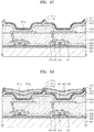
- FIG. 4 is a cross-sectional view illustrating an organic light-emitting display apparatus 400 according to another embodiment.
- the organic light-emitting display apparatus 400 includes a substrate 401, a thin film transistor (TFT), a first electrode 410, an intermediate layer 412, a second electrode 413, a first inorganic encapsulating layer 421, a first organic encapsulating layer 431, a second inorganic encapsulating layer 422, a second organic encapsulating layer 432, a third inorganic encapsulating layer 423, a third organic encapsulating layer 433, and a fourth inorganic encapsulating layer 424.
- TFT thin film transistor
- the TFT may include an active layer 403, a gate electrode 405, a source electrode 407, and a drain electrode 408. It is to be understood that the TFT may vary from what is disclosed herein.
- a buffer layer 402 may be formed on the substrate 401.
- the active layer 403 having a predetermined pattern may be formed on the buffer layer 402.
- the active layer 403 may be formed of an organic semiconductor or an inorganic semiconductor such as amorphous silicon or polysilicon, and may include a source region, a drain region, and a channel region.
- a gate insulating film 404 may be formed on the active layer 403.
- the gate electrode 405 may be formed on the gate insulating film 404.
- the gate insulating film 404 for insulating the active layer 403 from the gate electrode 405 may be formed of an organic material or an inorganic material such as SiN x or SiO 2 .
- the gate electrode 405 may include Au, Ag, Cu, Ni, Pt, Pd, Al, or Mo, or may include an alloy such as Al:Nd or Mo:W. Other suitable materials may be used.
- the gate electrode 405 may be formed of any of various materials by considering adhesion, flatness, electrical resistance, and processability with respect to an adjacent layer.
- An interlayer insulating film 406 may be formed on the gate electrode 405.
- the interlayer insulating film 406 and the gate insulating film 404 are formed to expose the source region and the drain region of the active layer 403, and the source electrode 407 and the drain electrode 408 are formed to contact the exposed source region and drain region of the active layer 403.
- Each of the source electrode 407 and the drain electrode 408 may be formed of any of various conductive materials, and may have a single-layer structure or a multi-layer structure.
- a passivation layer 409 may be formed on the source electrode 407 and the drain electrode 408.
- the passivation layer 409 may be formed to expose a portion of the drain electrode 408 without entirely covering the drain electrode 408, and the first electrode 410 is formed to be connected to the exposed portion of the drain electrode 408.
- a pixel defining film 419, the intermediate layer 412, and the second electrode 413 are formed on the first electrode 410. Also, the first inorganic encapsulating layer 421, the first organic encapsulating layer 431, the second inorganic encapsulating layer 422, the second organic encapsulating layer 432, the third inorganic encapsulating layer 423, the third organic encapsulating layer 433, and the fourth inorganic encapsulating layer 424 are formed, in particular on the first electrode 410, e.g. directly on the second electrode 413.
- the first inorganic encapsulating layer 421, the first organic encapsulating layer 431, the second inorganic encapsulating layer 422, the second organic encapsulating layer 432, the third inorganic encapsulating layer 423, the third organic encapsulating layer 433, and the fourth inorganic encapsulating layer 424 are the same as those described with reference to FIGS. 1 through 3 , and thus a detailed explanation thereof will not be repeated.
- the first inorganic encapsulating layer 421, the first organic encapsulating layer 431, the second inorganic encapsulating layer 422, the second organic encapsulating layer 432, the third inorganic encapsulating layer 423, the third organic encapsulating layer 433, and the fourth inorganic encapsulating layer 424 are sequentially stacked. Accordingly, the intermediate layer 412, the first electrode 410, and the second electrode 413 may be effectively protected.
- Top surfaces of the third organic encapsulating layer 433 and the fourth inorganic encapsulating layer 424 are flat so that the organic light-emitting display apparatus 400 may be easily coupled to an additional member such as a case member (not shown). Accordingly, industrial applicability may be improved. Also, visible light emitted from the intermediate layer 412 finally passes through the flat top surfaces to have uniform characteristics. Accordingly, image quality may be improved.
- FIGS. 5A through 5E are cross-sectional views illustrating stages of a method of manufacturing an organic light-emitting display apparatus, according to an embodiment.
- FIGS. 5A through 5E are cross-sectional views for explaining a method of manufacturing the organic light-emitting display apparatus 400 of FIG. 4 .
- the buffer layer 402 may be formed on the substrate 401
- the active layer 403 may be formed on the buffer layer 402
- the gate insulating film 404 may be formed on the active layer 403
- the gate electrode 405 may be formed on a predetermined portion of the gate insulating film 404
- the interlayer insulating film 406 may be formed on the gate electrode 405, and the source electrode 407 and the drain electrode 408 may be formed on the interlayer insulating film 406.
- the passivation layer 409 may be formed on the source electrode 407 and the drain electrode 408, the first electrode 410 may be formed on the passivation layer 409 to be connected to the drain electrode 408, and the pixel defining film 419 may be formed on the first electrode 410. In this case, at least one portion of a top surface of the first electrode 410 is not covered by the pixel defining film 419 and remains exposed.
- the intermediate layer 412 is formed.
- the intermediate layer 412 is formed to contact the first electrode 410.
- the intermediate layer 412 may be formed to correspond to the pixel defining film 419.
- the intermediate layer 412 may not be smooth and includes a protrusion 412c. As shown in FIG. 5B , a plurality of the intermediate layers 412 are formed to correspond to a plurality of the first electrodes 410, and the plurality of first electrodes 410 correspond to subpixels. The plurality of intermediate layers 412 may be provided to respectively correspond to the plurality of subpixels. In this case, at least one protrusion 412c may protrude from an edge of each of the plurality of intermediate layer 412.
- the intermediate layer 412 is formed by using an imaging process such as laser induced thermal imaging (LITI), the protrusion 412c is likely to be formed.
- the intermediate layer 412 may also be formed using any of various methods besides imaging.
- the second electrode 413 may be formed on the intermediate layer 412.
- the second electrode 413 does not completely cover the intermediate layer 412 such that the protrusion 412c of the intermediate layer 412 is exposed.
- a thickness of the protrusion 412c may be greater than a thickness of the second electrode 413. Accordingly, the protrusion 412c may not be completely covered by the second electrode 413.
- the first inorganic encapsulating layer 421 may be formed on the second electrode 413.
- the first inorganic encapsulating layer 421 includes a first groove 421g and a first protrusion 421c.
- the first protrusion 421c is disposed around the first groove 421g.
- the first protrusion 421c may be formed to correspond to the protrusion 412c of the intermediate layer 412.
- the first inorganic encapsulating layer 421 may not completely cover the intermediate layer 412.
- the protrusion 412c of the intermediate layer 412 which is not covered by the second electrode 413 to be exposed may not be covered by the first inorganic encapsulating layer 421 to be exposed.
- the protrusion 421c of the first inorganic encapsulating layer 421 corresponding to the protrusion 412c of the intermediate layer 412 may not completely cover the protrusion 412c, and thus the protrusion 412c of the intermediate layer 412 may be exposed.
- the first organic encapsulating layer 431, and the second inorganic encapsulating layer 422, the second organic encapsulating layer 432, the third inorganic encapsulating layer 423 are formed on the first inorganic encapsulating layer 421.
- the first organic encapsulating layer 431 is disposed on the first inorganic encapsulating layer 421.
- the first organic encapsulating layer 431 is disposed in the first groove 421g of the first inorganic encapsulating layer 421 so as not to extend beyond the first groove 421g.
- the first organic encapsulating layer 431 is spaced apart from the protrusion 412c of the intermediate layer 412. Accordingly, the first organic encapsulating layer 431 and the intermediate layer 412 may be prevented from contacting each other.
- the first organic encapsulating layer 431 is spaced apart from an uppermost portion of the first inorganic protrusion 421c of the first inorganic encapsulating layer 421.
- the second inorganic encapsulating layer 422 may be formed on the first organic encapsulating layer 431.
- the second inorganic encapsulating layer 422 covers the first organic encapsulating layer 431 and the first inorganic encapsulating layer 421.
- the second inorganic encapsulating layer 422 may be formed to cover the intermediate layer 412. Accordingly, the second inorganic encapsulating layer 422 may contact the protrusion 412c of the intermediate layer 412.
- the second inorganic encapsulating layer 422 may be formed to contact the first inorganic encapsulating layer 421 at at least one portion of the first inorganic encapsulating layer 421. That is, a portion of the first inorganic encapsulating layer 421 where the first organic encapsulating layer 431 does not contact the first inorganic encapsulating layer 421 contacts the second inorganic encapsulating layer 422.
- the second inorganic encapsulating layer 422 includes a second inorganic protrusion 422c corresponding to the first inorganic protrusion 421c of the first inorganic encapsulating layer 421.
- the second inorganic encapsulating layer 422 includes a second groove 422g.
- the second organic encapsulating layer 432 may be formed on the second inorganic encapsulating layer 422.
- the second organic encapsulating layer 432 is disposed in the second groove 422g of the second inorganic encapsulating layer 422 not to extend beyond the second groove 422g.
- the second organic encapsulating layer 432 is spaced apart from an uppermost portion of the second inorganic protrusion 422c of the second inorganic encapsulating layer 422.
- the third inorganic encapsulating layer 423 may be formed on the second organic encapsulating layer 432.
- the third inorganic encapsulating layer 423 covers the second organic encapsulating layer 432 and the second inorganic encapsulating layer 422.
- the third inorganic encapsulating layer 423 may be formed to contact the second inorganic encapsulating layer 422 at at least one portion of the second inorganic encapsulating layer 422. That is, a portion of the second inorganic encapsulating layer 422 where the second organic encapsulating layer 432 does not contact the second inorganic encapsulating layer 422 contacts the third inorganic encapsulating layer 423.
- the third organic encapsulating layer 433, and the fourth inorganic encapsulating layer 424 are formed.
- the third organic encapsulating layer 433 may be formed on the third inorganic encapsulating layer 423.
- the third organic encapsulating layer 433 having a flat top surface may be formed to planarize members disposed under the third organic encapsulating layer 433.
- the third organic encapsulating layer 433 may be formed to have a thickness greater than a thickness of each of the first organic encapsulating layer 431 and the second organic encapsulating layer 432.
- the fourth inorganic encapsulating layer 424 may be formed on the third organic encapsulating layer 433.
- the fourth inorganic encapsulating layer 424 covers the third organic encapsulating layer 433. Also, the fourth inorganic encapsulating layer 424 has a flat top surface.
- a typical organic light-emitting display apparatus includes an intermediate layer, a first electrode, and a second electrode.
- the intermediate layer includes an organic light-emitting layer, and the organic light-emitting layer generates visible light by applying a voltage to the first electrode and the second electrode.
- the intermediate layer which includes an organic material may be easily contaminated with an external foreign substance, moisture, or gas.
- the durability and electrical characteristics of the organic light-emitting display apparatus may be drastically degraded.
- an organic light-emitting display apparatus and a method of manufacturing the same may easily provide improved durability and electrical characteristics.
Landscapes
- Chemical & Material Sciences (AREA)
- Inorganic Chemistry (AREA)
- Physics & Mathematics (AREA)
- Optics & Photonics (AREA)
- Engineering & Computer Science (AREA)
- Manufacturing & Machinery (AREA)
- Electroluminescent Light Sources (AREA)
- Devices For Indicating Variable Information By Combining Individual Elements (AREA)
Claims (14)
- Eine organische lichtemittierende Anzeigevorrichtung (100), aufweisend:ein Substrat (101);eine erste Elektrode (110) auf dem Substrat (101);eine Zwischenschicht (112) auf der ersten Elektrode (110), wobei die Zwischenschicht (112) eine organische lichtemittierende Schicht aufweist;eine zweite Elektrode (113) auf der Zwischenschicht (112);eine erste anorganische Verkapselungsschicht (121) auf der zweiten Elektrode (113), wobei die erste anorganische Verkapselungsschicht (121) eine erste Nut (121g) definiert; undeine zweite anorganische Verkapselungsschicht (122) auf der ersten organischen Verkapselungsschicht (131), wobei die Zwischenschicht (112) einen Zwischenschichtvorsprung (112c) aufweist,dadurch gekennzeichnet, dassdie organische lichtemittierende Anzeigevorrichtung (100) eine erste organische Verkapselungsschicht (131) in der ersten Nut (121g), die von der ersten anorganischen Verkapselungsschicht (121) definiert ist, aufweist, wobei sich die erste organische Verkapselungsschicht (131) nicht über die erste Nut (121g) hinaus erstreckt.
- Die organische lichtemittierende Anzeigevorrichtung (100) nach Anspruch 1, wobei:die zweite Elektrode (113) vom Zwischenschichtvorsprung (112c) beabstandet ist, um den Zwischenschichtvorsprung (112c) nicht zu bedecken, unddie erste anorganische Verkapselungsschicht (121) vom Zwischenschichtvorsprung (112c) beabstandet ist, um den Zwischenschichtvorsprung (112c) nicht zu bedecken.
- Die organische lichtemittierende Anzeigevorrichtung (400) nach Anspruch 1 oder 2, wobei:die organische lichtemittierende Anzeigevorrichtung (400) eine Vielzahl von Subpixeln aufweist,eine Vielzahl der Zwischenschichten (112, 212, 312, 412) bereitgestellt sind, um mit der Vielzahl der Subpixel zu korrespondieren, undder Zwischenschichtvorsprung (112c, 212c, 412c) auf zumindest einem Rand jeder der Vielzahl der Zwischenschichten (112, 212, 312, 412) ist.
- Die organische lichtemittierende Anzeigevorrichtung nach einem der Ansprüche 1 bis 3, wobei:die erste anorganische Verkapselungsschicht (121) einen ersten anorganischen Vorsprung (121c), der dem Zwischenschichtvorsprung (112c) entspricht, aufweist, undder erste anorganische Vorsprung (121c) um die erste Nut (121g) herum angeordnet ist.
- Die organische lichtemittierende Anzeigevorrichtung (100) nach Anspruch 4, wobei die erste organische Verkapselungsschicht (113) von einem obersten Abschnitt des ersten anorganischen Vorsprungs (121c) oder vom Zwischenschichtvorsprung (112c) beabstandet ist.
- Die organische lichtemittierende Anzeigevorrichtung (200) nach einem der Ansprüche 1 bis 5, wobei zumindest ein Abschnitt des Zwischenschichtvorsprungs (212c) die zweite anorganische Verkapselungsschicht (232) kontaktiert.
- Die organische lichtemittierende Anzeigevorrichtung (100) nach einem der Ansprüche 1 bis 6, ferner aufweisend einen Pixeldefinitionsfilm, der auf der ersten Elektrode (110) angeordnet ist, um einen Abschnitt einer Oberseite der ersten Elektrode (110) nicht zu bedecken,
wobei der Zwischenschichtvorsprung (112c) angeordnet ist, um dem Pixeldefinitionsfilm (119) zu entsprechen. - Die organische lichtemittierende Anzeigevorrichtung (100) nach einem der Ansprüche 1 bis 7, wobei die erste anorganische Verkapselungsschicht (121) und die zweite anorganische Verkapselungsschicht (122) einander an zumindest einem Abschnitt der ersten anorganischen Verkapselungsschicht (121) kontatkieren
- Organische lichtemittierende Anzeigevorrichtung (200) nach einem der Ansprüche 1 bis 8, wobei:die zweite anorganische Verkapselungsschicht (222) eine zweite Nut (222g) definiert, unddie organische lichtemittierende Anzeigevorrichtung (200) ferner aufweist:eine zweite organische Verkapselungsschicht (232), die in der zweiten Nut (222g) der zweiten anorganischen Verkapselungsschicht (222) angeordnet ist, um sich nicht über die zweite Nut (222g) hinaus zu erstrecken; undeine dritte anorganische Verkapselungsschicht (223) auf der zweiten organischen Verkapselungsschicht (232).
- Die organische lichtemittierende Anzeigevorrichtung nach Anspruch 9, wobei die zweite anorganische Verkapselungsschicht (222) einen zweiten anorganischen Vorsprung (222c), der um die zweite Nut (222g) herum angeordnet ist, aufweist.
- Organische lichtemittierende Anzeigevorrichtung (300) nach Anspruch 9 oder 10, ferner aufweisend zumindest eine zusätzliche organische Verkapselungsschicht (333) und zumindest eine zusätzliche anorganische Verkapselungsschicht (324) auf der dritten anorganischen Verkapselungsschicht (323).
- Die organische lichtemittierende Anzeigevorrichtung (300) nach Anspruch 11, wobei eine Oberseite einer obersten organischen Verkapselungsschicht (333) der zumindest einen zusätzlichen organischen Verkapselungsschicht (333), die auf der dritten anorganischen Verkapselungsschicht (323) ausgebildet ist, flach ist.
- Die organische lichtemittierende Anzeigevorrichtung (300) nach Anspruch 11 oder 12, wobei eine Oberseite einer obersten anorganischen Verkapselungsschicht (321) aus der zumindest einen zusätzlichen anorganischen Verkapselungsschicht (321), die auf der dritten anorganischen Verkapselungsschicht (323) ausgebildet ist, flach ist.
- Ein Verfahren zum Herstellen einer organischen lichtemittierenden Anzeigevorrichtung (100), wobei das Verfahren aufweist:Ausbilden einer ersten Elektrode (110) auf einem Substrat (101);Ausbilden einer Zwischenschicht (112) auf der ersten Elektrode (110), wobei die Zwischenschicht (112) eine organische lichtemittierende Schicht auf der ersten Elektrode (110) aufweist;Ausbilden einer zweiten Elektrode (113) auf der Zwischenschicht (112);Ausbilden einer ersten anorganischen Verkapselungsschicht (121) auf der zweiten Elektrode (113), wobei die erste anorganische Verkapselungsschicht (121) eine erste Nut (121g) definiert;Ausbilden einer ersten organischen Verkapselungsschicht (113) in der ersten Nut (121g), die von der ersten anorganischen Verkapselungsschicht (121) definiert wird, so, dass sich die erste organische Verkapselungsschicht (131) nicht über die erste Nut (121g) hinaus erstreckt; undAusbilden einer zweiten anorganischen Verkapselungsschicht (122) auf der ersten organischen Verkapselungsschicht (131), wobei die Zwischenschicht (112) ausgebildet wird, um einen Zwischenschichtvorsprung (112c) aufzuweisen,dadurch gekennzeichnet, dassder Vorsprung (121c) der ersten anorganischen Verkapselungsschicht (121) ausgebildet wird, um dem Vorsprung (112c) der Zwischenschicht (112) zu entsprechen und, ebenso wie die zweite Elektrode (113), den Vorsprung (112c) der Zwischenschicht (112) nicht vollständig zu bedecken, wobei die zweite anorganische Verkapselungsschicht (122) ausgebildet wird, um den Vorsprung (112c) der Zwischenschicht (112) zu kontaktieren.
Applications Claiming Priority (1)
| Application Number | Priority Date | Filing Date | Title |
|---|---|---|---|
| KR1020110140402A KR101900364B1 (ko) | 2011-12-22 | 2011-12-22 | 유기 발광 표시 장치 및 유기 발광 표시 장치 제조 방법 |
Publications (2)
| Publication Number | Publication Date |
|---|---|
| EP2608288A1 EP2608288A1 (de) | 2013-06-26 |
| EP2608288B1 true EP2608288B1 (de) | 2017-06-21 |
Family
ID=46845630
Family Applications (1)
| Application Number | Title | Priority Date | Filing Date |
|---|---|---|---|
| EP12184787.5A Active EP2608288B1 (de) | 2011-12-22 | 2012-09-18 | Organische lichtemittierende Anzeigevorrichtung und Herstellungsverfahren dafür |
Country Status (6)
| Country | Link |
|---|---|
| US (1) | US8952360B2 (de) |
| EP (1) | EP2608288B1 (de) |
| JP (1) | JP6135975B2 (de) |
| KR (1) | KR101900364B1 (de) |
| CN (1) | CN103178078B (de) |
| TW (1) | TWI578512B (de) |
Families Citing this family (33)
| Publication number | Priority date | Publication date | Assignee | Title |
|---|---|---|---|---|
| JP6054763B2 (ja) * | 2013-02-12 | 2016-12-27 | 株式会社ジャパンディスプレイ | 有機el表示装置 |
| JP6139196B2 (ja) * | 2013-03-15 | 2017-05-31 | 株式会社ジャパンディスプレイ | 有機エレクトロルミネッセンス表示装置及び有機エレクトロルミネッセンス表示装置の製造方法 |
| KR20150011231A (ko) | 2013-07-22 | 2015-01-30 | 삼성디스플레이 주식회사 | 유기 발광 표시 장치 및 이의 제조 방법 |
| US9614021B2 (en) * | 2013-07-24 | 2017-04-04 | Samsung Display Co., Ltd. | Organic light-emitting display apparatus and manufacturing method thereof |
| KR102116105B1 (ko) | 2013-07-31 | 2020-05-28 | 삼성디스플레이 주식회사 | 가요성 표시 장치 |
| JP6169439B2 (ja) * | 2013-08-21 | 2017-07-26 | 株式会社ジャパンディスプレイ | 有機エレクトロルミネッセンス表示装置及びその製造方法 |
| JP6286941B2 (ja) | 2013-08-27 | 2018-03-07 | セイコーエプソン株式会社 | 発光装置、発光装置の製造方法、電子機器 |
| JP2015109192A (ja) * | 2013-12-04 | 2015-06-11 | 株式会社ジャパンディスプレイ | 有機エレクトロルミネッセンス表示装置 |
| JP6453579B2 (ja) * | 2014-08-08 | 2019-01-16 | 株式会社ジャパンディスプレイ | 有機el表示装置 |
| KR102352283B1 (ko) * | 2014-11-03 | 2022-01-18 | 삼성디스플레이 주식회사 | 유기발광 디스플레이 장치 |
| CN104538425B (zh) * | 2014-12-19 | 2018-01-12 | 上海天马微电子有限公司 | 一种阻挡膜及其制作方法、显示装置 |
| KR102456698B1 (ko) | 2015-01-15 | 2022-10-19 | 삼성디스플레이 주식회사 | 신축성 표시 장치 |
| CN104900681B (zh) * | 2015-06-09 | 2019-02-05 | 上海天马有机发光显示技术有限公司 | 有机发光显示面板及其形成方法 |
| KR102426710B1 (ko) * | 2015-11-03 | 2022-07-29 | 삼성디스플레이 주식회사 | 유기발광 디스플레이 장치 및 그 제조방법 |
| KR102444177B1 (ko) * | 2015-12-28 | 2022-09-19 | 삼성디스플레이 주식회사 | 유기 발광 표시 장치 및 이의 제조 방법 |
| JP2017157406A (ja) * | 2016-03-01 | 2017-09-07 | 株式会社ジャパンディスプレイ | 有機el表示装置 |
| CN105895827B (zh) * | 2016-06-28 | 2017-11-07 | 京东方科技集团股份有限公司 | 一种有机发光显示器件及其封装方法、显示装置 |
| KR102649240B1 (ko) | 2016-08-23 | 2024-03-21 | 삼성디스플레이 주식회사 | 표시 장치 및 이의 제조 방법 |
| CN107123751B (zh) * | 2017-04-28 | 2019-04-16 | 武汉华星光电技术有限公司 | 一种柔性有机发光二极管显示器及其制作方法 |
| CN108461645A (zh) * | 2018-02-09 | 2018-08-28 | 武汉华星光电半导体显示技术有限公司 | 一种用于柔性显示器件上的封装结构及制备方法 |
| EP3776681B1 (de) * | 2018-03-30 | 2025-10-08 | BOE Technology Group Co., Ltd. | Organische lichtemittierende diodenanzeigetafel und anzeigevorrichtung sowie herstellungsverfahren dafür |
| CN109166902A (zh) * | 2018-06-22 | 2019-01-08 | 友达光电股份有限公司 | 有机发光显示器 |
| CN110233168B (zh) * | 2018-06-22 | 2023-10-27 | 友达光电股份有限公司 | 有机发光显示器 |
| CN108899350A (zh) * | 2018-07-13 | 2018-11-27 | 京东方科技集团股份有限公司 | 一种显示面板及其封装方法、oled装置 |
| CN109285964B (zh) * | 2018-09-28 | 2021-07-30 | 云谷(固安)科技有限公司 | 柔性显示面板及其制备方法、柔性显示装置 |
| CN109616492B (zh) * | 2018-10-26 | 2020-11-06 | 武汉华星光电半导体显示技术有限公司 | 柔性显示面板、柔性显示装置和柔性显示面板的制备方法 |
| KR102745474B1 (ko) * | 2018-11-16 | 2024-12-20 | 엘지디스플레이 주식회사 | 유기 발광 표시 장치 |
| CN111647948B (zh) * | 2019-03-04 | 2022-02-01 | 中国科学院化学研究所 | 具有改善激子-光子耦合强度的有机半导体微纳晶体及其制备方法与应用 |
| CN110518143A (zh) * | 2019-08-19 | 2019-11-29 | 武汉华星光电半导体显示技术有限公司 | Oled显示面板及其制备方法 |
| CN110504385B (zh) | 2019-08-29 | 2022-04-15 | 京东方科技集团股份有限公司 | 一种显示面板、其制作方法及显示装置 |
| CN110581226B (zh) * | 2019-09-12 | 2022-03-22 | 云谷(固安)科技有限公司 | 柔性显示面板及其制备方法和柔性显示装置 |
| KR20230030718A (ko) * | 2021-08-25 | 2023-03-07 | 삼성디스플레이 주식회사 | 표시 장치 |
| EP4568458A4 (de) * | 2022-09-08 | 2025-12-17 | Samsung Electronics Co Ltd | Anzeigetafel mit lichtsteuerungsmaterial und elektronische vorrichtung |
Citations (1)
| Publication number | Priority date | Publication date | Assignee | Title |
|---|---|---|---|---|
| US20090021157A1 (en) * | 2007-07-18 | 2009-01-22 | Tae-Woong Kim | Organic light emitting display and method of manufacturing the same |
Family Cites Families (16)
| Publication number | Priority date | Publication date | Assignee | Title |
|---|---|---|---|---|
| US6815723B2 (en) * | 2001-12-28 | 2004-11-09 | Semiconductor Energy Laboratory Co., Ltd. | Light emitting device, method of manufacturing the same, and manufacturing apparatus therefor |
| US7109653B2 (en) * | 2002-01-15 | 2006-09-19 | Seiko Epson Corporation | Sealing structure with barrier membrane for electronic element, display device, electronic apparatus, and fabrication method for electronic element |
| US6933520B2 (en) * | 2002-02-13 | 2005-08-23 | Semiconductor Energy Laboratory Co., Ltd. | Light emitting device |
| KR100611768B1 (ko) * | 2004-10-11 | 2006-08-10 | 삼성에스디아이 주식회사 | 유기전계발광표시장치 및 그 제조방법 |
| KR100685413B1 (ko) | 2004-11-04 | 2007-02-22 | 삼성에스디아이 주식회사 | 레이저 전사용 도너 기판 및 이를 이용한 유기 전계 발광소자의 제조 방법 |
| KR100700836B1 (ko) * | 2005-11-16 | 2007-03-28 | 삼성에스디아이 주식회사 | 레이저 열 전사 장치 및 레이저 열 전사법 그리고 이를이용한 유기 발광소자의 제조방법 |
| JP5160754B2 (ja) * | 2006-01-31 | 2013-03-13 | エルジー ディスプレイ カンパニー リミテッド | El装置 |
| KR100730220B1 (ko) | 2006-06-02 | 2007-06-19 | 삼성에스디아이 주식회사 | 유기 발광 디스플레이 장치 |
| JP4652451B2 (ja) | 2006-08-10 | 2011-03-16 | パイオニア株式会社 | 光デバイス、および光デバイスの製造方法 |
| KR100759437B1 (ko) | 2006-11-09 | 2007-09-20 | 삼성에스디아이 주식회사 | 유기 발광 표시 장치 |
| TWI396464B (zh) * | 2007-01-22 | 2013-05-11 | Innolux Corp | 有機電致發光顯示裝置及其製作方法 |
| TW200915635A (en) | 2007-05-24 | 2009-04-01 | Koninkl Philips Electronics Nv | Encapsulation for an electronic thin film device |
| JP2009037812A (ja) * | 2007-07-31 | 2009-02-19 | Sumitomo Chemical Co Ltd | 有機el装置およびその製造方法 |
| JP2010287421A (ja) * | 2009-06-11 | 2010-12-24 | Toppan Printing Co Ltd | 有機el装置及びその製造方法 |
| JP5601025B2 (ja) * | 2010-05-21 | 2014-10-08 | セイコーエプソン株式会社 | 電気光学装置及び電気光学装置の製造方法、並びに電子機器 |
| KR101805753B1 (ko) * | 2011-06-13 | 2017-12-08 | 삼성디스플레이 주식회사 | 유기 발광 표시 장치 |
-
2011
- 2011-12-22 KR KR1020110140402A patent/KR101900364B1/ko active Active
-
2012
- 2012-07-19 US US13/552,847 patent/US8952360B2/en active Active
- 2012-08-21 TW TW101130335A patent/TWI578512B/zh active
- 2012-08-21 CN CN201210298858.1A patent/CN103178078B/zh active Active
- 2012-09-18 EP EP12184787.5A patent/EP2608288B1/de active Active
- 2012-12-18 JP JP2012275965A patent/JP6135975B2/ja active Active
Patent Citations (1)
| Publication number | Priority date | Publication date | Assignee | Title |
|---|---|---|---|---|
| US20090021157A1 (en) * | 2007-07-18 | 2009-01-22 | Tae-Woong Kim | Organic light emitting display and method of manufacturing the same |
Also Published As
| Publication number | Publication date |
|---|---|
| CN103178078B (zh) | 2017-04-12 |
| EP2608288A1 (de) | 2013-06-26 |
| US8952360B2 (en) | 2015-02-10 |
| KR101900364B1 (ko) | 2018-09-20 |
| KR20130072808A (ko) | 2013-07-02 |
| TWI578512B (zh) | 2017-04-11 |
| JP6135975B2 (ja) | 2017-05-31 |
| US20130161680A1 (en) | 2013-06-27 |
| CN103178078A (zh) | 2013-06-26 |
| JP2013134989A (ja) | 2013-07-08 |
| TW201327802A (zh) | 2013-07-01 |
Similar Documents
| Publication | Publication Date | Title |
|---|---|---|
| EP2608288B1 (de) | Organische lichtemittierende Anzeigevorrichtung und Herstellungsverfahren dafür | |
| US8895972B2 (en) | Display device and organic light emitting display device having auxiliary electrode | |
| US8193017B2 (en) | Organic light emitting display device and method of manufacturing the same | |
| EP2811522B1 (de) | Organische lichtemittierende Anzeigevorrichtung | |
| US10056575B2 (en) | Flexible display apparatus, organic light emitting display apparatus, and mother substrate for flexible display apparatus | |
| US9287339B2 (en) | Organic light emitting display device and method of manufacturing the same | |
| TWI549284B (zh) | 有機發光顯示裝置及其製造方法 | |
| US8981362B2 (en) | Organic light-emitting display device and method of manufacturing the same | |
| EP2530717A2 (de) | Organische lichtemittierende Anzeigevorrichtung und Verfahren zu deren Herstellung | |
| EP2738830A2 (de) | Organische lichtemittierende Anzeigevorrichtung und Herstellungsverfahren dafür | |
| US8530888B2 (en) | Organic light-emitting display device and method of manufacturing the same | |
| CN105742322A (zh) | 显示装置 | |
| KR20110101771A (ko) | 유기 발광 표시장치 | |
| US20140097407A1 (en) | Organic light emitting display apparatus and method of manufacturing the same | |
| EP3035407B1 (de) | Anzeigevorrichtung | |
| US8399284B2 (en) | Method of manufacturing the organic light-emitting display | |
| US20140014914A1 (en) | Organic light-emitting display device and method of manufacturing the same | |
| US10211425B2 (en) | Display device and method of manufacturing the same | |
| US20130200378A1 (en) | Method and apparatus for forming organic material pattern, organic light emitting display apparatus, and method of manufacturing organic light emitting display apparatus |
Legal Events
| Date | Code | Title | Description |
|---|---|---|---|
| AK | Designated contracting states |
Kind code of ref document: A1 Designated state(s): AL AT BE BG CH CY CZ DE DK EE ES FI FR GB GR HR HU IE IS IT LI LT LU LV MC MK MT NL NO PL PT RO RS SE SI SK SM TR |
|
| AX | Request for extension of the european patent |
Extension state: BA ME |
|
| PUAI | Public reference made under article 153(3) epc to a published international application that has entered the european phase |
Free format text: ORIGINAL CODE: 0009012 |
|
| 17P | Request for examination filed |
Effective date: 20130819 |
|
| RBV | Designated contracting states (corrected) |
Designated state(s): AL AT BE BG CH CY CZ DE DK EE ES FI FR GB GR HR HU IE IS IT LI LT LU LV MC MK MT NL NO PL PT RO RS SE SI SK SM TR |
|
| 17Q | First examination report despatched |
Effective date: 20150312 |
|
| RAP1 | Party data changed (applicant data changed or rights of an application transferred) |
Owner name: SAMSUNG DISPLAY CO., LTD. |
|
| GRAP | Despatch of communication of intention to grant a patent |
Free format text: ORIGINAL CODE: EPIDOSNIGR1 |
|
| STAA | Information on the status of an ep patent application or granted ep patent |
Free format text: STATUS: GRANT OF PATENT IS INTENDED |
|
| INTG | Intention to grant announced |
Effective date: 20170207 |
|
| GRAS | Grant fee paid |
Free format text: ORIGINAL CODE: EPIDOSNIGR3 |
|
| GRAA | (expected) grant |
Free format text: ORIGINAL CODE: 0009210 |
|
| STAA | Information on the status of an ep patent application or granted ep patent |
Free format text: STATUS: THE PATENT HAS BEEN GRANTED |
|
| AK | Designated contracting states |
Kind code of ref document: B1 Designated state(s): AL AT BE BG CH CY CZ DE DK EE ES FI FR GB GR HR HU IE IS IT LI LT LU LV MC MK MT NL NO PL PT RO RS SE SI SK SM TR |
|
| REG | Reference to a national code |
Ref country code: GB Ref legal event code: FG4D |
|
| REG | Reference to a national code |
Ref country code: CH Ref legal event code: EP |
|
| REG | Reference to a national code |
Ref country code: IE Ref legal event code: FG4D |
|
| REG | Reference to a national code |
Ref country code: AT Ref legal event code: REF Ref document number: 903656 Country of ref document: AT Kind code of ref document: T Effective date: 20170715 |
|
| REG | Reference to a national code |
Ref country code: DE Ref legal event code: R096 Ref document number: 602012033645 Country of ref document: DE |
|
| REG | Reference to a national code |
Ref country code: FR Ref legal event code: PLFP Year of fee payment: 6 |
|
| REG | Reference to a national code |
Ref country code: NL Ref legal event code: FP |
|
| PG25 | Lapsed in a contracting state [announced via postgrant information from national office to epo] |
Ref country code: GR Free format text: LAPSE BECAUSE OF FAILURE TO SUBMIT A TRANSLATION OF THE DESCRIPTION OR TO PAY THE FEE WITHIN THE PRESCRIBED TIME-LIMIT Effective date: 20170922 Ref country code: FI Free format text: LAPSE BECAUSE OF FAILURE TO SUBMIT A TRANSLATION OF THE DESCRIPTION OR TO PAY THE FEE WITHIN THE PRESCRIBED TIME-LIMIT Effective date: 20170621 Ref country code: HR Free format text: LAPSE BECAUSE OF FAILURE TO SUBMIT A TRANSLATION OF THE DESCRIPTION OR TO PAY THE FEE WITHIN THE PRESCRIBED TIME-LIMIT Effective date: 20170621 Ref country code: NO Free format text: LAPSE BECAUSE OF FAILURE TO SUBMIT A TRANSLATION OF THE DESCRIPTION OR TO PAY THE FEE WITHIN THE PRESCRIBED TIME-LIMIT Effective date: 20170921 Ref country code: LT Free format text: LAPSE BECAUSE OF FAILURE TO SUBMIT A TRANSLATION OF THE DESCRIPTION OR TO PAY THE FEE WITHIN THE PRESCRIBED TIME-LIMIT Effective date: 20170621 |
|
| REG | Reference to a national code |
Ref country code: LT Ref legal event code: MG4D |
|
| REG | Reference to a national code |
Ref country code: AT Ref legal event code: MK05 Ref document number: 903656 Country of ref document: AT Kind code of ref document: T Effective date: 20170621 |
|
| PG25 | Lapsed in a contracting state [announced via postgrant information from national office to epo] |
Ref country code: RS Free format text: LAPSE BECAUSE OF FAILURE TO SUBMIT A TRANSLATION OF THE DESCRIPTION OR TO PAY THE FEE WITHIN THE PRESCRIBED TIME-LIMIT Effective date: 20170621 Ref country code: LV Free format text: LAPSE BECAUSE OF FAILURE TO SUBMIT A TRANSLATION OF THE DESCRIPTION OR TO PAY THE FEE WITHIN THE PRESCRIBED TIME-LIMIT Effective date: 20170621 Ref country code: BG Free format text: LAPSE BECAUSE OF FAILURE TO SUBMIT A TRANSLATION OF THE DESCRIPTION OR TO PAY THE FEE WITHIN THE PRESCRIBED TIME-LIMIT Effective date: 20170921 Ref country code: SE Free format text: LAPSE BECAUSE OF FAILURE TO SUBMIT A TRANSLATION OF THE DESCRIPTION OR TO PAY THE FEE WITHIN THE PRESCRIBED TIME-LIMIT Effective date: 20170621 |
|
| PG25 | Lapsed in a contracting state [announced via postgrant information from national office to epo] |
Ref country code: AT Free format text: LAPSE BECAUSE OF FAILURE TO SUBMIT A TRANSLATION OF THE DESCRIPTION OR TO PAY THE FEE WITHIN THE PRESCRIBED TIME-LIMIT Effective date: 20170621 Ref country code: CZ Free format text: LAPSE BECAUSE OF FAILURE TO SUBMIT A TRANSLATION OF THE DESCRIPTION OR TO PAY THE FEE WITHIN THE PRESCRIBED TIME-LIMIT Effective date: 20170621 Ref country code: EE Free format text: LAPSE BECAUSE OF FAILURE TO SUBMIT A TRANSLATION OF THE DESCRIPTION OR TO PAY THE FEE WITHIN THE PRESCRIBED TIME-LIMIT Effective date: 20170621 Ref country code: SK Free format text: LAPSE BECAUSE OF FAILURE TO SUBMIT A TRANSLATION OF THE DESCRIPTION OR TO PAY THE FEE WITHIN THE PRESCRIBED TIME-LIMIT Effective date: 20170621 Ref country code: RO Free format text: LAPSE BECAUSE OF FAILURE TO SUBMIT A TRANSLATION OF THE DESCRIPTION OR TO PAY THE FEE WITHIN THE PRESCRIBED TIME-LIMIT Effective date: 20170621 |
|
| PG25 | Lapsed in a contracting state [announced via postgrant information from national office to epo] |
Ref country code: IS Free format text: LAPSE BECAUSE OF FAILURE TO SUBMIT A TRANSLATION OF THE DESCRIPTION OR TO PAY THE FEE WITHIN THE PRESCRIBED TIME-LIMIT Effective date: 20171021 Ref country code: SM Free format text: LAPSE BECAUSE OF FAILURE TO SUBMIT A TRANSLATION OF THE DESCRIPTION OR TO PAY THE FEE WITHIN THE PRESCRIBED TIME-LIMIT Effective date: 20170621 Ref country code: ES Free format text: LAPSE BECAUSE OF FAILURE TO SUBMIT A TRANSLATION OF THE DESCRIPTION OR TO PAY THE FEE WITHIN THE PRESCRIBED TIME-LIMIT Effective date: 20170621 Ref country code: PL Free format text: LAPSE BECAUSE OF FAILURE TO SUBMIT A TRANSLATION OF THE DESCRIPTION OR TO PAY THE FEE WITHIN THE PRESCRIBED TIME-LIMIT Effective date: 20170621 Ref country code: IT Free format text: LAPSE BECAUSE OF FAILURE TO SUBMIT A TRANSLATION OF THE DESCRIPTION OR TO PAY THE FEE WITHIN THE PRESCRIBED TIME-LIMIT Effective date: 20170621 |
|
| REG | Reference to a national code |
Ref country code: DE Ref legal event code: R097 Ref document number: 602012033645 Country of ref document: DE |
|
| PLBE | No opposition filed within time limit |
Free format text: ORIGINAL CODE: 0009261 |
|
| STAA | Information on the status of an ep patent application or granted ep patent |
Free format text: STATUS: NO OPPOSITION FILED WITHIN TIME LIMIT |
|
| PG25 | Lapsed in a contracting state [announced via postgrant information from national office to epo] |
Ref country code: DK Free format text: LAPSE BECAUSE OF FAILURE TO SUBMIT A TRANSLATION OF THE DESCRIPTION OR TO PAY THE FEE WITHIN THE PRESCRIBED TIME-LIMIT Effective date: 20170621 |
|
| REG | Reference to a national code |
Ref country code: CH Ref legal event code: PL |
|
| 26N | No opposition filed |
Effective date: 20180322 |
|
| PG25 | Lapsed in a contracting state [announced via postgrant information from national office to epo] |
Ref country code: MC Free format text: LAPSE BECAUSE OF FAILURE TO SUBMIT A TRANSLATION OF THE DESCRIPTION OR TO PAY THE FEE WITHIN THE PRESCRIBED TIME-LIMIT Effective date: 20170621 |
|
| REG | Reference to a national code |
Ref country code: IE Ref legal event code: MM4A |
|
| REG | Reference to a national code |
Ref country code: BE Ref legal event code: MM Effective date: 20170930 |
|
| PG25 | Lapsed in a contracting state [announced via postgrant information from national office to epo] |
Ref country code: LU Free format text: LAPSE BECAUSE OF NON-PAYMENT OF DUE FEES Effective date: 20170918 |
|
| PG25 | Lapsed in a contracting state [announced via postgrant information from national office to epo] |
Ref country code: LI Free format text: LAPSE BECAUSE OF NON-PAYMENT OF DUE FEES Effective date: 20170930 Ref country code: IE Free format text: LAPSE BECAUSE OF NON-PAYMENT OF DUE FEES Effective date: 20170918 Ref country code: CH Free format text: LAPSE BECAUSE OF NON-PAYMENT OF DUE FEES Effective date: 20170930 |
|
| REG | Reference to a national code |
Ref country code: FR Ref legal event code: PLFP Year of fee payment: 7 |
|
| PG25 | Lapsed in a contracting state [announced via postgrant information from national office to epo] |
Ref country code: BE Free format text: LAPSE BECAUSE OF NON-PAYMENT OF DUE FEES Effective date: 20170930 Ref country code: SI Free format text: LAPSE BECAUSE OF FAILURE TO SUBMIT A TRANSLATION OF THE DESCRIPTION OR TO PAY THE FEE WITHIN THE PRESCRIBED TIME-LIMIT Effective date: 20170621 |
|
| PG25 | Lapsed in a contracting state [announced via postgrant information from national office to epo] |
Ref country code: MT Free format text: LAPSE BECAUSE OF NON-PAYMENT OF DUE FEES Effective date: 20170918 |
|
| PG25 | Lapsed in a contracting state [announced via postgrant information from national office to epo] |
Ref country code: HU Free format text: LAPSE BECAUSE OF FAILURE TO SUBMIT A TRANSLATION OF THE DESCRIPTION OR TO PAY THE FEE WITHIN THE PRESCRIBED TIME-LIMIT; INVALID AB INITIO Effective date: 20120918 |
|
| PG25 | Lapsed in a contracting state [announced via postgrant information from national office to epo] |
Ref country code: CY Free format text: LAPSE BECAUSE OF NON-PAYMENT OF DUE FEES Effective date: 20170621 |
|
| PG25 | Lapsed in a contracting state [announced via postgrant information from national office to epo] |
Ref country code: MK Free format text: LAPSE BECAUSE OF FAILURE TO SUBMIT A TRANSLATION OF THE DESCRIPTION OR TO PAY THE FEE WITHIN THE PRESCRIBED TIME-LIMIT Effective date: 20170621 |
|
| PG25 | Lapsed in a contracting state [announced via postgrant information from national office to epo] |
Ref country code: TR Free format text: LAPSE BECAUSE OF FAILURE TO SUBMIT A TRANSLATION OF THE DESCRIPTION OR TO PAY THE FEE WITHIN THE PRESCRIBED TIME-LIMIT Effective date: 20170621 |
|
| PG25 | Lapsed in a contracting state [announced via postgrant information from national office to epo] |
Ref country code: PT Free format text: LAPSE BECAUSE OF FAILURE TO SUBMIT A TRANSLATION OF THE DESCRIPTION OR TO PAY THE FEE WITHIN THE PRESCRIBED TIME-LIMIT Effective date: 20170621 |
|
| PG25 | Lapsed in a contracting state [announced via postgrant information from national office to epo] |
Ref country code: AL Free format text: LAPSE BECAUSE OF FAILURE TO SUBMIT A TRANSLATION OF THE DESCRIPTION OR TO PAY THE FEE WITHIN THE PRESCRIBED TIME-LIMIT Effective date: 20170621 |
|
| REG | Reference to a national code |
Ref country code: DE Ref legal event code: R079 Ref document number: 602012033645 Country of ref document: DE Free format text: PREVIOUS MAIN CLASS: H01L0051520000 Ipc: H10K0050800000 |
|
| P01 | Opt-out of the competence of the unified patent court (upc) registered |
Effective date: 20230515 |
|
| PGFP | Annual fee paid to national office [announced via postgrant information from national office to epo] |
Ref country code: NL Payment date: 20250821 Year of fee payment: 14 |
|
| PGFP | Annual fee paid to national office [announced via postgrant information from national office to epo] |
Ref country code: DE Payment date: 20250820 Year of fee payment: 14 |
|
| PGFP | Annual fee paid to national office [announced via postgrant information from national office to epo] |
Ref country code: GB Payment date: 20250820 Year of fee payment: 14 |
|
| PGFP | Annual fee paid to national office [announced via postgrant information from national office to epo] |
Ref country code: FR Payment date: 20250821 Year of fee payment: 14 |