EP2603974B1 - Switched-mode power supply apparatus and method - Google Patents
Switched-mode power supply apparatus and method Download PDFInfo
- Publication number
- EP2603974B1 EP2603974B1 EP11754508.7A EP11754508A EP2603974B1 EP 2603974 B1 EP2603974 B1 EP 2603974B1 EP 11754508 A EP11754508 A EP 11754508A EP 2603974 B1 EP2603974 B1 EP 2603974B1
- Authority
- EP
- European Patent Office
- Prior art keywords
- load
- voltage
- switching
- power amplifier
- switched
- Prior art date
- Legal status (The legal status is an assumption and is not a legal conclusion. Google has not performed a legal analysis and makes no representation as to the accuracy of the status listed.)
- Not-in-force
Links
- 238000000034 method Methods 0.000 title claims description 12
- 238000004088 simulation Methods 0.000 description 22
- 238000005259 measurement Methods 0.000 description 16
- 239000004065 semiconductor Substances 0.000 description 13
- 238000013459 approach Methods 0.000 description 8
- 238000010586 diagram Methods 0.000 description 7
- 238000002595 magnetic resonance imaging Methods 0.000 description 5
- 230000035945 sensitivity Effects 0.000 description 4
- 239000003990 capacitor Substances 0.000 description 3
- 238000012937 correction Methods 0.000 description 3
- 230000001419 dependent effect Effects 0.000 description 3
- 238000005070 sampling Methods 0.000 description 3
- 238000004458 analytical method Methods 0.000 description 2
- 230000006870 function Effects 0.000 description 2
- 230000005484 gravity Effects 0.000 description 2
- 230000008569 process Effects 0.000 description 2
- 230000001133 acceleration Effects 0.000 description 1
- 238000003491 array Methods 0.000 description 1
- 230000008901 benefit Effects 0.000 description 1
- 238000009529 body temperature measurement Methods 0.000 description 1
- 238000004364 calculation method Methods 0.000 description 1
- 230000008859 change Effects 0.000 description 1
- 230000007423 decrease Effects 0.000 description 1
- 238000013461 design Methods 0.000 description 1
- 238000011161 development Methods 0.000 description 1
- 238000005516 engineering process Methods 0.000 description 1
- 230000001939 inductive effect Effects 0.000 description 1
- 230000003071 parasitic effect Effects 0.000 description 1
- 238000012545 processing Methods 0.000 description 1
- 230000007704 transition Effects 0.000 description 1
- 238000013519 translation Methods 0.000 description 1
- 239000002699 waste material Substances 0.000 description 1
Images





Classifications
-
- H—ELECTRICITY
- H03—ELECTRONIC CIRCUITRY
- H03F—AMPLIFIERS
- H03F3/00—Amplifiers with only discharge tubes or only semiconductor devices as amplifying elements
- H03F3/20—Power amplifiers, e.g. Class B amplifiers, Class C amplifiers
- H03F3/21—Power amplifiers, e.g. Class B amplifiers, Class C amplifiers with semiconductor devices only
- H03F3/217—Class D power amplifiers; Switching amplifiers
-
- G—PHYSICS
- G01—MEASURING; TESTING
- G01R—MEASURING ELECTRIC VARIABLES; MEASURING MAGNETIC VARIABLES
- G01R33/00—Arrangements or instruments for measuring magnetic variables
- G01R33/20—Arrangements or instruments for measuring magnetic variables involving magnetic resonance
- G01R33/28—Details of apparatus provided for in groups G01R33/44 - G01R33/64
- G01R33/38—Systems for generation, homogenisation or stabilisation of the main or gradient magnetic field
- G01R33/385—Systems for generation, homogenisation or stabilisation of the main or gradient magnetic field using gradient magnetic field coils
- G01R33/3852—Gradient amplifiers; means for controlling the application of a gradient magnetic field to the sample, e.g. a gradient signal synthesizer
-
- H—ELECTRICITY
- H03—ELECTRONIC CIRCUITRY
- H03F—AMPLIFIERS
- H03F3/00—Amplifiers with only discharge tubes or only semiconductor devices as amplifying elements
- H03F3/20—Power amplifiers, e.g. Class B amplifiers, Class C amplifiers
- H03F3/21—Power amplifiers, e.g. Class B amplifiers, Class C amplifiers with semiconductor devices only
- H03F3/217—Class D power amplifiers; Switching amplifiers
- H03F3/2173—Class D power amplifiers; Switching amplifiers of the bridge type
-
- H—ELECTRICITY
- H03—ELECTRONIC CIRCUITRY
- H03K—PULSE TECHNIQUE
- H03K7/00—Modulating pulses with a continuously-variable modulating signal
- H03K7/08—Duration or width modulation ; Duty cycle modulation
-
- H—ELECTRICITY
- H02—GENERATION; CONVERSION OR DISTRIBUTION OF ELECTRIC POWER
- H02M—APPARATUS FOR CONVERSION BETWEEN AC AND AC, BETWEEN AC AND DC, OR BETWEEN DC AND DC, AND FOR USE WITH MAINS OR SIMILAR POWER SUPPLY SYSTEMS; CONVERSION OF DC OR AC INPUT POWER INTO SURGE OUTPUT POWER; CONTROL OR REGULATION THEREOF
- H02M1/00—Details of apparatus for conversion
- H02M1/08—Circuits specially adapted for the generation of control voltages for semiconductor devices incorporated in static converters
- H02M1/088—Circuits specially adapted for the generation of control voltages for semiconductor devices incorporated in static converters for the simultaneous control of series or parallel connected semiconductor devices
-
- H—ELECTRICITY
- H02—GENERATION; CONVERSION OR DISTRIBUTION OF ELECTRIC POWER
- H02M—APPARATUS FOR CONVERSION BETWEEN AC AND AC, BETWEEN AC AND DC, OR BETWEEN DC AND DC, AND FOR USE WITH MAINS OR SIMILAR POWER SUPPLY SYSTEMS; CONVERSION OF DC OR AC INPUT POWER INTO SURGE OUTPUT POWER; CONTROL OR REGULATION THEREOF
- H02M1/00—Details of apparatus for conversion
- H02M1/38—Means for preventing simultaneous conduction of switches
- H02M1/385—Means for preventing simultaneous conduction of switches with means for correcting output voltage deviations introduced by the dead time
Definitions
- the present invention relates to a switched-mode power supply apparatus and a corresponding method. Further, the present invention relates to a device comprising a load to be provided with a load voltage and/or load current.
- Switching power amplifiers often are afflicted with non-linearities due to the switching behavior of the output stage.
- the exact nature of these non-linearities not only depends on the type of power semiconductor(s) used, but also on the connected circuit(s) at load and driving side.
- precision power applications such as for example motion control and gradient amplifiers for magnetic resonance imaging (MRI)
- compensation of these non-linearities is mandatory because a feed-forward path is in most cases used in the control system.
- US 2006/208798 A1 discloses a method of operating a class D amplifier output stage that compensates for nonlinearity introduced by a residual load current during the dead time in the switching of the output stage.
- the amplifier output stage includes an input, a gate driver circuit, two output transistors, an output, and a current sensing circuit.
- the transistors are serially connected between the terminals of a power supply.
- a residual load current flows through the transistors when they are switched off.
- the gate driver circuit increases or decreases the duty cycles of signals driving the transistors based on the direction of the residual load current flowing through the transistors, thereby causing the duty cycle of the amplifier output to remain substantially constant and equal to the duty cycle of the amplifier input.
- a possible method to fill such a look-up table is to repeatedly simulate the circuit off-line for all combinations of the parameters mentioned above and store the resulting average voltage in a look-up table.
- An appropriate compensation of the switch timings can be found by using look-up table entries and, if needed, use interpolation to find an approximation of the circuit behavior for exactly the combination of circuit states which has been measured by the controller at the beginning of the control time interval.
- Such a solution is possible in principle, but will, if implemented in full, need considerable memory resources. Even with the abundance of cheap memory devices available today, such an approach is limited in accuracy and the number of state variables which can be used due to the exponential growth laws inherent in such an approach.
- Other linearization techniques are found in US2007/0152750 , US2008/0180166 , GB2357915 , US6593806 , and US5617058 .
- a switched-mode power supply apparatus comprising:
- a device comprising a load to be provided with a load voltage and/or load current is presented, said device comprising:
- the invention proposes an alternative approach for reliable compensation of non-linearities caused by dead-time and voltage drops in switching power amplifiers by using in-the-loop simulation on an accelerated time scale.
- the size of the circuitry (for example based on field-programmable gate arrays, FPGAs) necessary to do this shows linear growth with respect to the complexity of the circuits to represent, due to the parallel processing inherent to such an implementation. Acceleration with a factor 10 appears to be readily possible with present-day devices. For example, such an implementation would allow the prediction of the next 20 microseconds (a typical value for the control and/or switching cycle for the innermost control loop in the systems mentioned above) in 2 microseconds or less.
- the signal supplied by the external signal source mentioned here may be a power signal provided by a power source, but is generally a set point, which is typically supplied by a "master" controller on an insignificant power level.
- said control unit is adapted for selecting the timing settings for controlling the switching of said switching power amplifier from the timing settings used for predicting the average load voltage and/or load current by selecting the timing setting belonging to a predicted average load voltage and/or load current closest to the desired load voltage and/or load current. In this way a high accuracy of the prediction can generally be obtained.
- control unit is adapted for determining the timing setting for controlling the switching of said switching power amplifier by interpolating between the timing settings belonging to predicted average load voltages and/or load currents closest to the desired load voltage and/or load current. By such an interpolation the optimal timing setting can be obtained.
- said control unit comprises a sampled control circuit for determining the desired load voltage and/or load current from the state information about the present state of the switching power amplifier and a set point.
- Said sampled control circuit is particularly adapted for periodically providing the desired output voltage of the amplifier based on a combination of set point and measurement signals.
- said control unit is adapted for predicting the average supply voltage and/or supply current for a predetermined number of timing settings, in particular for a number in the range from 2 to 25 of timing settings. 2 to 25 are reasonable numbers, but other numbers can be implemented in practice as well.
- the switched-mode power supply apparatus may further comprise sensing means for sensing said state information about the present state of the switching power amplifier, in particular for sensing internal currents and/or voltages of the switching power amplifier and/or the temperature of one or more elements of the power amplifier and/or the power supply apparatus.
- sensing means are generally implemented by commonly known means, such as current measurement elements, voltage measurement elements, temperature measurement elements, etc.
- a prediction method for example based on the use of a physical model of the circuit and/or device behavior, can also be used. Such an approach is particularly interesting for measurement of the temperature of the semiconductor junctions, which are almost not accessible with commonly known means.
- control unit may be adapted for predicting the average load voltage and/or load current for the next switching period with high fidelity. This is especially important if the switching power amplifier is used in a feed-forward control chain.
- control unit is adapted for predicting the average load voltage and/or load current for a subsequent time interval, in particular equal to a control cycle or in the range from 1 to 200, in particular from 5 to 50 ⁇ sec.
- Switching power amplifiers often are afflicted with non-linearities due to the switching behavior of the output stage.
- precision power applications such as used for precise motion control and in the gradient system of magnetic resonance imaging (MRI) apparatus
- compensation of these non-linearities is mandatory because a feed-forward path is in most cases used in the control system.
- the non-linear behavior is mainly caused by the non-zero time it takes to switch off one semiconductor in a phase leg and switch on the other one.
- a so-called dead time is introduced between the switching off and on events, to create some tolerance for timing differences between different incarnations of the power semiconductors, the driving stages, and circuit states.
- both power semiconductors are turned off, and the voltage on the switching node is mainly determined by the output current (while the initial state (voltage) of the switching node is generally relevant as well).
- the average voltage during a certain time span is important. This average voltage also depends on the switching node voltage during the dead time.
- a phase leg, built up with Insulated Gate Bipolar Transistors (IGBTs) and diodes is shown in Fig. 1 .
- the phase leg is supplied with a DC voltage V_sup from a voltage source, and loaded with a DC output current I_bridge from a current source.
- the combined capacitance on the switching node is shown as a single capacitor Cnode.
- a measurement device mVnode is incorporated to show the definition of the switching node voltage as shown in subsequent figures.
- the voltage on the switching node shows varying behavior.
- the IGBTs are implemented as ideal switches with series resistance 100m ⁇ . This is a rather crude model, which is used only to illustrate the main phenomena which cause non-linearities. In reality, the detailed switching behavior of the power semiconductors and the non-linearity of the parasitic device capacitances which are represented by Cnode in Fig. 1 need to be taken into account.
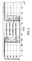
- the shapes of the node voltage versus time for this example are shown in Fig. 2 .
- the timing (switching on/off) of the power semiconductors has been set such that a nominal duty cycle of 60% and a dead time of 2 ⁇ s are used.
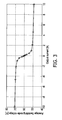
- the switching node voltage during the dead time interval, and thereby also the average of this voltage over a switching cycle depends on the sign and magnitude of the output current. This dependence is shown in Fig. 3 .
- the most significant variation of the average voltage i.e. the swing of almost 20 volts between -2A and +2A output current
- the dead time i.e. the swing of almost 20 volts between -2A and +2A output current
- a finite slope can be observed for higher current values. This slope is mainly caused by the voltage drop due to the resistive behavior of the power semiconductors, while the influence of the voltage commutation is also present, but above a few amperes in this example much smaller than the resistive voltage drop.
- the drop or boost of the average node voltage as shown in Fig. 3 can be compensated for by adjusting the duty cycle of the gate signals which drive the power semiconductors.
- the table values as shown in Fig. 3 can be used to change the timing of the switching events such that the average node voltage for the interval considered in this example (i.e. 20 ⁇ s) is corrected.
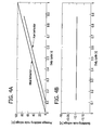
- the amount of (timing) correction needed can be found by evaluating the dependence of the average switching node voltage on the duty cycle. For the case of a constant-current load of 5A, this has been depicted in Fig. 4 .
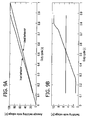
- Fig. 5 The shape of the switching node voltage after applying the compensation is shown in Fig. 5 .
- the compensation can lead to almost perfect results, the set point value of 60 volts can be realized to within a few mV.
- the resulting average phase leg voltage is shown in Fig. 6 .
- FIG. 7 A typical load circuit, as used in de gradient chain of an MRI scanner, is shown in Fig. 7 .
- the load circuit comprises a filter inductance Lfilt, filter capacitor Cfilt, and a gradient coil Lgrad.
- the filter inductance is approximately 5% of the gradient coil inductance.
- the circuit has been configured with the following exemplary parameters: Name Value Meaning Vdc 100 [V] DC supply voltage I_Vf 1 [V] IGBT equivalent forward voltage drop I_Rf 10 [m ⁇ ] IGBT equivalent differential resistance D_Vf 1 [V] Diode equivalent forward voltage drop D_Rf 10 [m ⁇ ] Diode equivalent differential resistance Cnode 2 [nF] Capacitance on switching node Lfilt 25 [ ⁇ H] Filter inductance Cfilt 10 [ ⁇ F] Filter capacitance Lgrad 500 [ ⁇ H] Gradient coil inductance
- Fig. 8 An example of such a situation is shown in Fig. 8 .
- the filter coil current depicted in Fig. 8B crosses through zero during the first dead-time interval.
- the node voltage depicted in Fig. 8A shows a glitch of significant width (ca. 1.1 ⁇ s).
- the development of the switching node voltage over time depends on all initial values of the circuit states (Vnode, Ifilt, Vfilt, Igrad), the supply voltage, and the instants of switching of both power semiconductors, i.e. a number (e.g. seven) of parameters.
- the operating temperatures of several circuit elements can come into play. Due to the resulting complexity of the circuit, an analytical solution of the network problem is not feasible. Still, to eliminate the non-linearities of the circuit, it is desirable to predict the average switching node voltage over the next interval of interest.
- the average value of the switching node voltage no longer shows linear dependence on the duty cycle. In fact, this value depends on all circuit states and the switching instants in a complex manner.
- the average phase leg voltage for one particular initial situation (the same as used for Fig. 8 ) has been computed by means of simulation for a range of values for the duty cycle. The results are shown in Fig. 9 , wherein Fig. 9A shows plots for the true and the ideal behavior of the average switching node voltage and Fig. 9B shows the difference between true and ideal behavior on an enlarged scale.
- Fig. 10 shows a schematic a block diagram of the general layout of a switched-mode power supply apparatus 10.
- a controller 12 gets from an external signal source 11 as a system input a set point representing the desired output voltage or current and measurement signals measured at the output of a power amplifier 14, said measurement signals representing current(s) and/or voltage(s) that shall be reproduced similar to the set point.
- Which signals need to be measured depends on a variety of choices, such as the desired accuracy and the details of the power circuit. In the following it is assumed that circuit states associated with energy-storing circuit elements (i.e. capacitor voltages and inductor currents) are measured, but other choices are possible.
- the controller 12 uses the information from the set point signal and the actual measurement signals to control the switching of power semiconductors provided in the amplifier 14.
- the power amplifier 14 comprises power circuitry and power semiconductors for generation of the desired output signal(s) based on the input control signals.
- the output signal(s) are generally a load voltage and/or a load current, which are provided to an external load 15.
- FIG. 11 An exemplary embodiment of the power amplifier 14 is depicted in Fig. 11 .
- This circuit can be used as a current amplifier.
- the current through the load coil Lload is the controlled variable.
- this particular circuit will be used as an example for a power amplifier, but it should be noted that the present invention can be applied to other power amplifiers using different circuit configurations (topologies) as well.
- the controller 12a comprises a sampled control circuit 16 and a PWM modulator 18, which translates the desired voltage to timing signals.
- the sampled control circuit 16 uses a combination of the set point and measurement signals to periodically provide the desired average output voltage (for the next control cycle / time interval) of the amplifier 14.
- Inside the sampled control circuit usually a combination of feedforward and feedback control is used to obtain the desired result.
- Such a sampled control circuit is, for instance, described in "Control Systems Engineering” by Norman S. Nise, John Wiley & Sons, so that the details of it will not be explained here.
- An important feature here is that the control is sampled. Sampling implies that measurement data is obtained at certain instances, in most cases at a fixed frequency. Due to the sampling, measurement information "in between" the sampling instants is not available, and all actions (in this context decisions about switching events) are therefore necessarily based on "old" information.
- the technique used by the modulator is generally known and, for instance, described in http://en.wikipedia.org/wiki/Pulse-width_modulation and "Pulse width modulation for power converters: principles and practice” by D. Grahame Holmes, Thomas A. Lipo, T. A. Lipo, Wiley-IEEE, 2003 .
- the present invention is directed to the function of the PWM modulator 18 shown in Fig. 12 .
- the average voltage produced by the amplifier 14 not only depends on the PWM timing, but also on the load condition, in particular the actual output current as illustrated in Fig. 3 .
- the circuit behavior can deviate even more from the desired case, as shown in Fig. 9 .
- the controller 12a As shown in Fig. 12 , is modified as shown in Fig. 13 showing an embodiment of a controller 12b according to the present invention, which can be used as controller 12 shown in the power supply apparatus 10 depicted in Fig. 10 .
- the sampled control circuit 20 is substantially identical to the sampled control circuit 16 of the controller 12a, but the PWM modulator 18 has been replaced by a simulation unit 22 and an interpolator 24.
- the operation of control circuit 12b is as follows.
- this value together with the measurements of all relevant power circuit signals (in most cases this will comprise complete or partial "state information", i.e. signals associated with energy-storing circuit elements, which is provided via the input "in_measurements" are used by the simulation unit 22 in an accelerated simulation ("accelerated” being used here to imply that the simulation result for a full control cycle is ready well before the control cycle has passed in real time) to predict the average output voltage of the power amplifier 14 for a variety of timing settings, schematically indicated with A,B,..., Z in Fig. 13 . How many of these timing settings are really needed depends on the desired accuracy and details of the power amplifier.
- Input "in_U" of the simulation unit 22 can, optionally, be used to restrict the number of timing settings, for example using advance knowledge about the maximum deviation from the "ideal" PWM modulator briefly described above.
- Clock_minus_sim_delay produces a trigger a time "accelerated_sim_delay" before the clock as defined in the earlier controller. So, the output of the latter is precisely the original clock.
- the "in_measurements” i.e. the "state information" contains circuit signals (including supply voltage(s)), some of which can possibly be predicted instead of measured.
- the power amplifier 14 is fitted with optional sensors 13 (as schematically shown in Fig. 11 ) to provide all those circuit signals.
- sensors 13 as schematically shown in Fig. 11 .
- the power amplifier 14 is fitted with optional sensors 13 (as schematically shown in Fig. 11 ) to provide all those circuit signals.
- sensors 13 as schematically shown in Fig. 11 .
- the average output voltage is predicted for a variety of timing settings. There are various possibilities where the timing settings come from. The most crude and resource-hungry approach would be to generate a fixed number of time settings (that would be internal in the "Accelerated_Simulation" unit 22) and compute the resulting voltages.
- the output of the simulation unit 22 comprises a number of predicted output voltages, one value for each timing setting.
- this information is used to obtain the optimal timing setting, which, when applied to the power amplifier 14, will generate the desired output voltage. This process is illustrated in Fig. 14 .
- This setting can now be applied to the gate trigger signals of the power amplifier 14, and it will, depending on the detail and accuracy of the simulation model and the timing points chosen in the graph shown in Fig. 14 , reproduce the desired output voltage with high fidelity.
- An embodiment of the present invention is thus a hardware circuit simulation on accelerated time scale.
- the circuit is simulated using a (circuit) model of the behavior.
- This model can be either analogue or digital, but in the following a digital (FPGA) version is considered as this is by far the most flexible solution with present-day technology.
- the simulation model to be implemented comprises differential equations obtained by elementary circuit analysis, combined with details of the switching behavior.
- These differential equations are then discretized using appropriate time step(s) and a discrete (difference equation) solver, which must be robust for the Eigen values (time constants) of interest in the circuit. This discretization process is generally known in the art, and has been described for example in " K. Watanabe, D. M. Himmelblau "Analysis of trajectory errors in integrating ordinary differential equations", Journal of the Franklin Institute, Volume 314, Issue 5, November 1982, Pages 283-321, ISSN 0016-0032 .
- the difference equations can be simulated with acceptable accuracy using time steps of 10ns. If the difference equations describing the discretized behavior are now executed on a 1ns clock, which appears to be well within reach of actual FPGA devices, a result 10 times (i.e. 10ns/1ns) faster than in real time can be obtained. In other words, when 10% of the cycle time (2 ⁇ s in the example above) has passed, an estimate of the average voltage produced by the phase leg over the complete cycle (20 ⁇ s) is achieved, which can still be corrected by adjusting one or more of the switching events in time.
- the simulation in the example would execute in 2000 (2 ⁇ s/1ns) steps.
- a variable time step is used for the simulation model in an embodiment. Simulations have shown that using an appropriate variable-step solver, a solution can be found already using ca. 1000 steps, so within 1 ⁇ s in the example.
- the simulation provides the average switch node voltage for a certain setting of the duty cycle. To be able to compensate this voltage by means of the switch timing (i.e. the timing settings as described above), the sensitivity of this voltage to switch timing changes needs to be found. This sensitivity is the slope of the "true behavior" curves as shown in Fig. 4 and Fig. 9 .
- a possible approach is to run two or more simulation models in parallel, using perturbed values for the switch timing events.
- several identical models with different switch timings are used, each generating a single average voltage. These are then used in the interpolator 24 to retrieve the timing which should reproduce U_desired.
- the differences in outcome between the models are a direct indication of the sensitivity of the average switch node voltage to timing changes. This sensitivity can then be used for the voltage compensation.
- the number of such parallel models to run is limited in essence, as only small corrections to the timing are targeted.
- the present invention has been illustrated above with examples originating in a voltage-fed, current-output amplifier such as often applied in drives using magnetic motors and applications involving a load coil.
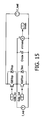
- the approach proposed according to the present invention is also valid for power amplifiers supplied by a current source and with a capacitive load, which at the typical switching frequency behaves like a voltage source.
- a simplified embodiment of such an application is shown in Fig. 15 , where the amplifier is supplied with power by a current source I_sup and the load circuit has been drawn as a voltage source V_load.
- the present invention is preferably used in switching power amplifiers in applications where feed-forward is used in the current or voltage control loop.
- Examples are MRI gradient current amplifiers, motion control amplifiers such as presently used in ASML (PAAC, PADC) and Assembléon products, and audio amplifiers supplying capacitive loud speakers.
Landscapes
- Physics & Mathematics (AREA)
- Engineering & Computer Science (AREA)
- Power Engineering (AREA)
- Condensed Matter Physics & Semiconductors (AREA)
- General Physics & Mathematics (AREA)
- Amplifiers (AREA)
- Dc-Dc Converters (AREA)
- Magnetic Resonance Imaging Apparatus (AREA)
Priority Applications (1)
| Application Number | Priority Date | Filing Date | Title |
|---|---|---|---|
| EP11754508.7A EP2603974B1 (en) | 2010-08-13 | 2011-08-05 | Switched-mode power supply apparatus and method |
Applications Claiming Priority (3)
| Application Number | Priority Date | Filing Date | Title |
|---|---|---|---|
| EP10172725 | 2010-08-13 | ||
| EP11754508.7A EP2603974B1 (en) | 2010-08-13 | 2011-08-05 | Switched-mode power supply apparatus and method |
| PCT/IB2011/053500 WO2012020363A1 (en) | 2010-08-13 | 2011-08-05 | Switched-mode power supply apparatus and method |
Publications (2)
| Publication Number | Publication Date |
|---|---|
| EP2603974A1 EP2603974A1 (en) | 2013-06-19 |
| EP2603974B1 true EP2603974B1 (en) | 2015-03-25 |
Family
ID=44583227
Family Applications (1)
| Application Number | Title | Priority Date | Filing Date |
|---|---|---|---|
| EP11754508.7A Not-in-force EP2603974B1 (en) | 2010-08-13 | 2011-08-05 | Switched-mode power supply apparatus and method |
Country Status (7)
| Country | Link |
|---|---|
| US (1) | US8937820B2 (enExample) |
| EP (1) | EP2603974B1 (enExample) |
| JP (1) | JP5937074B2 (enExample) |
| CN (1) | CN103069714B (enExample) |
| IN (1) | IN2013CN01310A (enExample) |
| RU (1) | RU2571393C2 (enExample) |
| WO (1) | WO2012020363A1 (enExample) |
Cited By (1)
| Publication number | Priority date | Publication date | Assignee | Title |
|---|---|---|---|---|
| WO2017216057A1 (en) * | 2016-06-16 | 2017-12-21 | Koninklijke Philips N.V. | Magnetic field gradient coil assembly with integrated modulator and switch unit |
Families Citing this family (9)
| Publication number | Priority date | Publication date | Assignee | Title |
|---|---|---|---|---|
| EP2656092B1 (en) * | 2010-12-20 | 2015-07-15 | Koninklijke Philips N.V. | State space feedback controller in the digital domain for an mri gradient coil power supply |
| US8773196B2 (en) * | 2011-09-30 | 2014-07-08 | Clevech Corporation | Resource pooling amplifier |
| HUE029292T2 (en) | 2011-12-20 | 2017-02-28 | ERICSSON TELEFON AB L M (publ) | Transmitter, transceiver, communication device, method and computer program |
| CN104142483B (zh) * | 2013-05-07 | 2017-07-07 | 辽宁开普医疗系统有限公司 | 一种高压大电流小纹波梯度放大器 |
| KR102141207B1 (ko) | 2013-11-11 | 2020-08-05 | 삼성디스플레이 주식회사 | 디스플레이 장치, 전원 전압 생성 장치, 및 전원 전압 생성 방법 |
| CN107005150B (zh) * | 2014-12-18 | 2019-10-11 | 皇家飞利浦有限公司 | 用于驱动负载的功率设备和方法 |
| NL2015303B1 (en) * | 2015-08-13 | 2017-02-28 | Prodrive Tech Bv | Electric power converter and MRI system comprising such converter. |
| EP3196713B2 (de) * | 2016-01-19 | 2024-06-26 | dSPACE GmbH | Simulationsvorrichtung zur simulation |
| JP7106252B2 (ja) * | 2017-06-26 | 2022-07-26 | キヤノンメディカルシステムズ株式会社 | 磁気共鳴イメージング装置 |
Family Cites Families (24)
| Publication number | Priority date | Publication date | Assignee | Title |
|---|---|---|---|---|
| JP2762279B2 (ja) * | 1988-09-30 | 1998-06-04 | ジーイー横河メディカルシステム株式会社 | 核磁気共鳴装置 |
| US5617058A (en) * | 1995-11-13 | 1997-04-01 | Apogee Technology, Inc. | Digital signal processing for linearization of small input signals to a tri-state power switch |
| US5764024A (en) * | 1997-04-07 | 1998-06-09 | Motorola, Inc. | Pulse width modulator (PWM) system with low cost dead time distortion correction |
| DE19837439C2 (de) * | 1998-08-18 | 2000-07-13 | Siemens Ag | Verfahren und Vorrichtung zum Erzeugen von Ansteuersignalen für eine Leistungsendstufe und Leistungsendstufe |
| US6294954B1 (en) | 1999-09-23 | 2001-09-25 | Audiologic, Incorporated | Adaptive dead time control for switching circuits |
| GB2357915B (en) | 1999-12-30 | 2001-12-05 | John Francis Hope | A scheme for correcting distortion in an all-digital power amplifier |
| JP2002064971A (ja) * | 2000-08-17 | 2002-02-28 | Taiyo Yuden Co Ltd | 混成集積回路装置 |
| US6859739B2 (en) | 2001-01-19 | 2005-02-22 | Smartsignal Corporation | Global state change indicator for empirical modeling in condition based monitoring |
| US6593806B1 (en) * | 2001-08-10 | 2003-07-15 | Cirrus Logic, Inc. | Circuits and methods for compensating switched mode amplifiers |
| RU2212729C1 (ru) * | 2002-01-08 | 2003-09-20 | Государственное унитарное предприятие "Всероссийский электротехнический институт им. В.И.Ленина" | Коммутатор и устройство для питания нагрузки знакопеременным напряжением на его основе |
| TW576007B (en) * | 2002-09-20 | 2004-02-11 | Richtek Technology Corp | Semi-simulating current sensing apparatus and method for switching mode DC/DC power source converter |
| JP4209266B2 (ja) * | 2003-06-17 | 2009-01-14 | 三菱電機株式会社 | リアルタイムシミュレーション装置およびリアルタイムシミュレーション方法 |
| US7345442B2 (en) * | 2003-09-02 | 2008-03-18 | Nsk Ltd. | Device for controlling electric-motor power steering device |
| FI119406B (fi) * | 2005-02-11 | 2008-10-31 | Abb Oy | Menetelmä ja järjestely taajuusmuuttajan yhteydessä |
| US7151406B2 (en) | 2005-03-15 | 2006-12-19 | Texas Instruments Incorporated | Compensation of nonlinearity introduced by dead time in switching output stage |
| RU2292627C1 (ru) * | 2005-06-30 | 2007-01-27 | Государственное образовательное учреждение высшего профессионального образования "Таганрогский государственный радиотехнический университет" (ТРТУ) | Источник вторичного электропитания с компенсацией искажений в питающей сети |
| DE102005048464B4 (de) | 2005-10-07 | 2014-11-06 | Dspace Digital Signal Processing And Control Engineering Gmbh | Verfahren und Vorrichtung zum Simulieren einer induktiven Last |
| US7286009B2 (en) | 2005-12-30 | 2007-10-23 | D2Audio Corporation | Digital PWM amplifier with simulation-based feedback |
| JP4749874B2 (ja) * | 2006-01-30 | 2011-08-17 | 日立オートモティブシステムズ株式会社 | 電力変換装置及びそれを用いたモータ駆動装置 |
| JP4762824B2 (ja) * | 2006-08-10 | 2011-08-31 | 株式会社豊田中央研究所 | 電力変換回路 |
| DE102006055577B4 (de) * | 2006-11-21 | 2014-03-20 | Ihp Gmbh - Innovations For High Performance Microelectronics / Leibniz-Institut Für Innovative Mikroelektronik | Sigma-Delta-Modulator mit Rückkopplung für Leistungsverstärker |
| JP2008259090A (ja) * | 2007-04-09 | 2008-10-23 | Olympus Corp | 増幅回路及び増幅回路装置 |
| US7979223B2 (en) | 2007-06-15 | 2011-07-12 | University Of South Carolina | Systems and methods for power hardware in the loop testing |
| JP2009077523A (ja) * | 2007-09-20 | 2009-04-09 | Diamond Electric Mfg Co Ltd | デジタルコンバータ及びその制御方法 |
-
2011
- 2011-08-05 IN IN1310CHN2013 patent/IN2013CN01310A/en unknown
- 2011-08-05 US US13/814,256 patent/US8937820B2/en active Active
- 2011-08-05 WO PCT/IB2011/053500 patent/WO2012020363A1/en not_active Ceased
- 2011-08-05 CN CN201180039028.0A patent/CN103069714B/zh not_active Expired - Fee Related
- 2011-08-05 EP EP11754508.7A patent/EP2603974B1/en not_active Not-in-force
- 2011-08-05 JP JP2013523690A patent/JP5937074B2/ja not_active Expired - Fee Related
- 2011-08-05 RU RU2013110831/08A patent/RU2571393C2/ru active
Cited By (1)
| Publication number | Priority date | Publication date | Assignee | Title |
|---|---|---|---|---|
| WO2017216057A1 (en) * | 2016-06-16 | 2017-12-21 | Koninklijke Philips N.V. | Magnetic field gradient coil assembly with integrated modulator and switch unit |
Also Published As
| Publication number | Publication date |
|---|---|
| CN103069714A (zh) | 2013-04-24 |
| EP2603974A1 (en) | 2013-06-19 |
| US8937820B2 (en) | 2015-01-20 |
| IN2013CN01310A (enExample) | 2015-08-07 |
| RU2571393C2 (ru) | 2015-12-20 |
| US20130127532A1 (en) | 2013-05-23 |
| WO2012020363A1 (en) | 2012-02-16 |
| RU2013110831A (ru) | 2014-09-20 |
| CN103069714B (zh) | 2016-05-04 |
| JP2013535946A (ja) | 2013-09-12 |
| JP5937074B2 (ja) | 2016-06-22 |
Similar Documents
| Publication | Publication Date | Title |
|---|---|---|
| US8937820B2 (en) | Switched-mode power supply apparatus and method | |
| KR101429415B1 (ko) | 적응 제어를 위한 방법 및 시스템 | |
| Celikovic et al. | Modeling of capacitor voltage imbalance in flying capacitor multilevel dc-dc converters | |
| KR101423871B1 (ko) | 시험장치 | |
| US9374081B2 (en) | Method for driving a load | |
| CN103973109B (zh) | 直接驱动波形放大器 | |
| NL2015303B1 (en) | Electric power converter and MRI system comprising such converter. | |
| WO2010029709A1 (ja) | 試験装置、試験方法、回路システム、ならびに電源装置、電源評価装置、電源環境のエミュレート方法 | |
| JP6591854B2 (ja) | シミュレータ、シミュレーションシステム、シミュレーション方法、および、プログラム | |
| Bizzarri et al. | A nonlinear inductance model able to reproduce thermal transient in SMPS simulations | |
| US10024937B2 (en) | Gradient amplifier with compensation for dead time and forward voltage | |
| Babaloo et al. | Nonlinear droop compensation for current waveforms in MRI gradient systems | |
| JP2015047021A (ja) | 電力変換装置のデットタイム補償装置 | |
| CN110048584B (zh) | 确定及补偿功率晶体管延迟 | |
| Wu et al. | Closed-loop slew rate control of active current source gate driver with digital implementation for SiC MOSFET | |
| JP5277671B2 (ja) | モータ駆動装置 | |
| Maas et al. | Control concepts for dielectric elastomer actuators | |
| US7667537B2 (en) | Method for correcting a harmonic distortion of a power bridge, in particular for a class D amplifier | |
| Babaloo et al. | Droop compensation of gradient current waveforms in gradient array systems | |
| CN105099254A (zh) | 一种直流-交流逆变器的控制方法 | |
| Hu et al. | Adaptive deadtime compensation for magnetic resonance imaging driver | |
| Ma et al. | SNS low-level RF control system: Design and performance | |
| WO2003056580A1 (en) | Improvements relating to operation of a current controller | |
| Janke et al. | Large-signal input characteristics of selected DC–DC switching converters, Part II. Discontinuous conduction mode | |
| JP2019165558A (ja) | スイッチング制御回路 |
Legal Events
| Date | Code | Title | Description |
|---|---|---|---|
| PUAI | Public reference made under article 153(3) epc to a published international application that has entered the european phase |
Free format text: ORIGINAL CODE: 0009012 |
|
| 17P | Request for examination filed |
Effective date: 20130313 |
|
| AK | Designated contracting states |
Kind code of ref document: A1 Designated state(s): AL AT BE BG CH CY CZ DE DK EE ES FI FR GB GR HR HU IE IS IT LI LT LU LV MC MK MT NL NO PL PT RO RS SE SI SK SM TR |
|
| RAP1 | Party data changed (applicant data changed or rights of an application transferred) |
Owner name: KONINKLIJKE PHILIPS N.V. |
|
| DAX | Request for extension of the european patent (deleted) | ||
| GRAP | Despatch of communication of intention to grant a patent |
Free format text: ORIGINAL CODE: EPIDOSNIGR1 |
|
| INTG | Intention to grant announced |
Effective date: 20141015 |
|
| GRAS | Grant fee paid |
Free format text: ORIGINAL CODE: EPIDOSNIGR3 |
|
| GRAA | (expected) grant |
Free format text: ORIGINAL CODE: 0009210 |
|
| AK | Designated contracting states |
Kind code of ref document: B1 Designated state(s): AL AT BE BG CH CY CZ DE DK EE ES FI FR GB GR HR HU IE IS IT LI LT LU LV MC MK MT NL NO PL PT RO RS SE SI SK SM TR |
|
| REG | Reference to a national code |
Ref country code: GB Ref legal event code: FG4D |
|
| REG | Reference to a national code |
Ref country code: CH Ref legal event code: EP |
|
| REG | Reference to a national code |
Ref country code: IE Ref legal event code: FG4D |
|
| REG | Reference to a national code |
Ref country code: DE Ref legal event code: R096 Ref document number: 602011015064 Country of ref document: DE Effective date: 20150507 |
|
| REG | Reference to a national code |
Ref country code: AT Ref legal event code: REF Ref document number: 718397 Country of ref document: AT Kind code of ref document: T Effective date: 20150515 |
|
| REG | Reference to a national code |
Ref country code: GB Ref legal event code: 746 Effective date: 20150427 |
|
| PG25 | Lapsed in a contracting state [announced via postgrant information from national office to epo] |
Ref country code: FI Free format text: LAPSE BECAUSE OF FAILURE TO SUBMIT A TRANSLATION OF THE DESCRIPTION OR TO PAY THE FEE WITHIN THE PRESCRIBED TIME-LIMIT Effective date: 20150325 Ref country code: HR Free format text: LAPSE BECAUSE OF FAILURE TO SUBMIT A TRANSLATION OF THE DESCRIPTION OR TO PAY THE FEE WITHIN THE PRESCRIBED TIME-LIMIT Effective date: 20150325 Ref country code: SE Free format text: LAPSE BECAUSE OF FAILURE TO SUBMIT A TRANSLATION OF THE DESCRIPTION OR TO PAY THE FEE WITHIN THE PRESCRIBED TIME-LIMIT Effective date: 20150325 Ref country code: LT Free format text: LAPSE BECAUSE OF FAILURE TO SUBMIT A TRANSLATION OF THE DESCRIPTION OR TO PAY THE FEE WITHIN THE PRESCRIBED TIME-LIMIT Effective date: 20150325 |
|
| REG | Reference to a national code |
Ref country code: AT Ref legal event code: MK05 Ref document number: 718397 Country of ref document: AT Kind code of ref document: T Effective date: 20150325 |
|
| REG | Reference to a national code |
Ref country code: LT Ref legal event code: MG4D |
|
| PG25 | Lapsed in a contracting state [announced via postgrant information from national office to epo] |
Ref country code: RS Free format text: LAPSE BECAUSE OF FAILURE TO SUBMIT A TRANSLATION OF THE DESCRIPTION OR TO PAY THE FEE WITHIN THE PRESCRIBED TIME-LIMIT Effective date: 20150325 Ref country code: GR Free format text: LAPSE BECAUSE OF FAILURE TO SUBMIT A TRANSLATION OF THE DESCRIPTION OR TO PAY THE FEE WITHIN THE PRESCRIBED TIME-LIMIT Effective date: 20150626 Ref country code: LV Free format text: LAPSE BECAUSE OF FAILURE TO SUBMIT A TRANSLATION OF THE DESCRIPTION OR TO PAY THE FEE WITHIN THE PRESCRIBED TIME-LIMIT Effective date: 20150325 |
|
| PG25 | Lapsed in a contracting state [announced via postgrant information from national office to epo] |
Ref country code: NL Free format text: LAPSE BECAUSE OF FAILURE TO SUBMIT A TRANSLATION OF THE DESCRIPTION OR TO PAY THE FEE WITHIN THE PRESCRIBED TIME-LIMIT Effective date: 20150325 |
|
| PG25 | Lapsed in a contracting state [announced via postgrant information from national office to epo] |
Ref country code: RO Free format text: LAPSE BECAUSE OF FAILURE TO SUBMIT A TRANSLATION OF THE DESCRIPTION OR TO PAY THE FEE WITHIN THE PRESCRIBED TIME-LIMIT Effective date: 20150325 Ref country code: SK Free format text: LAPSE BECAUSE OF FAILURE TO SUBMIT A TRANSLATION OF THE DESCRIPTION OR TO PAY THE FEE WITHIN THE PRESCRIBED TIME-LIMIT Effective date: 20150325 Ref country code: EE Free format text: LAPSE BECAUSE OF FAILURE TO SUBMIT A TRANSLATION OF THE DESCRIPTION OR TO PAY THE FEE WITHIN THE PRESCRIBED TIME-LIMIT Effective date: 20150325 Ref country code: CZ Free format text: LAPSE BECAUSE OF FAILURE TO SUBMIT A TRANSLATION OF THE DESCRIPTION OR TO PAY THE FEE WITHIN THE PRESCRIBED TIME-LIMIT Effective date: 20150325 Ref country code: ES Free format text: LAPSE BECAUSE OF FAILURE TO SUBMIT A TRANSLATION OF THE DESCRIPTION OR TO PAY THE FEE WITHIN THE PRESCRIBED TIME-LIMIT Effective date: 20150325 Ref country code: PT Free format text: LAPSE BECAUSE OF FAILURE TO SUBMIT A TRANSLATION OF THE DESCRIPTION OR TO PAY THE FEE WITHIN THE PRESCRIBED TIME-LIMIT Effective date: 20150727 |
|
| PG25 | Lapsed in a contracting state [announced via postgrant information from national office to epo] |
Ref country code: PL Free format text: LAPSE BECAUSE OF FAILURE TO SUBMIT A TRANSLATION OF THE DESCRIPTION OR TO PAY THE FEE WITHIN THE PRESCRIBED TIME-LIMIT Effective date: 20150325 Ref country code: IS Free format text: LAPSE BECAUSE OF FAILURE TO SUBMIT A TRANSLATION OF THE DESCRIPTION OR TO PAY THE FEE WITHIN THE PRESCRIBED TIME-LIMIT Effective date: 20150725 Ref country code: AT Free format text: LAPSE BECAUSE OF FAILURE TO SUBMIT A TRANSLATION OF THE DESCRIPTION OR TO PAY THE FEE WITHIN THE PRESCRIBED TIME-LIMIT Effective date: 20150325 |
|
| REG | Reference to a national code |
Ref country code: DE Ref legal event code: R097 Ref document number: 602011015064 Country of ref document: DE |
|
| PG25 | Lapsed in a contracting state [announced via postgrant information from national office to epo] |
Ref country code: DK Free format text: LAPSE BECAUSE OF FAILURE TO SUBMIT A TRANSLATION OF THE DESCRIPTION OR TO PAY THE FEE WITHIN THE PRESCRIBED TIME-LIMIT Effective date: 20150325 |
|
| PLBE | No opposition filed within time limit |
Free format text: ORIGINAL CODE: 0009261 |
|
| STAA | Information on the status of an ep patent application or granted ep patent |
Free format text: STATUS: NO OPPOSITION FILED WITHIN TIME LIMIT |
|
| 26N | No opposition filed |
Effective date: 20160105 |
|
| PG25 | Lapsed in a contracting state [announced via postgrant information from national office to epo] |
Ref country code: MC Free format text: LAPSE BECAUSE OF FAILURE TO SUBMIT A TRANSLATION OF THE DESCRIPTION OR TO PAY THE FEE WITHIN THE PRESCRIBED TIME-LIMIT Effective date: 20150325 Ref country code: LU Free format text: LAPSE BECAUSE OF FAILURE TO SUBMIT A TRANSLATION OF THE DESCRIPTION OR TO PAY THE FEE WITHIN THE PRESCRIBED TIME-LIMIT Effective date: 20150805 |
|
| REG | Reference to a national code |
Ref country code: CH Ref legal event code: PL |
|
| PG25 | Lapsed in a contracting state [announced via postgrant information from national office to epo] |
Ref country code: IT Free format text: LAPSE BECAUSE OF FAILURE TO SUBMIT A TRANSLATION OF THE DESCRIPTION OR TO PAY THE FEE WITHIN THE PRESCRIBED TIME-LIMIT Effective date: 20150325 Ref country code: CH Free format text: LAPSE BECAUSE OF NON-PAYMENT OF DUE FEES Effective date: 20150831 Ref country code: LI Free format text: LAPSE BECAUSE OF NON-PAYMENT OF DUE FEES Effective date: 20150831 |
|
| PG25 | Lapsed in a contracting state [announced via postgrant information from national office to epo] |
Ref country code: SI Free format text: LAPSE BECAUSE OF FAILURE TO SUBMIT A TRANSLATION OF THE DESCRIPTION OR TO PAY THE FEE WITHIN THE PRESCRIBED TIME-LIMIT Effective date: 20150325 |
|
| REG | Reference to a national code |
Ref country code: IE Ref legal event code: MM4A |
|
| PG25 | Lapsed in a contracting state [announced via postgrant information from national office to epo] |
Ref country code: IE Free format text: LAPSE BECAUSE OF NON-PAYMENT OF DUE FEES Effective date: 20150805 |
|
| REG | Reference to a national code |
Ref country code: FR Ref legal event code: PLFP Year of fee payment: 6 |
|
| PG25 | Lapsed in a contracting state [announced via postgrant information from national office to epo] |
Ref country code: BE Free format text: LAPSE BECAUSE OF FAILURE TO SUBMIT A TRANSLATION OF THE DESCRIPTION OR TO PAY THE FEE WITHIN THE PRESCRIBED TIME-LIMIT Effective date: 20150325 |
|
| PG25 | Lapsed in a contracting state [announced via postgrant information from national office to epo] |
Ref country code: MT Free format text: LAPSE BECAUSE OF FAILURE TO SUBMIT A TRANSLATION OF THE DESCRIPTION OR TO PAY THE FEE WITHIN THE PRESCRIBED TIME-LIMIT Effective date: 20150325 |
|
| PG25 | Lapsed in a contracting state [announced via postgrant information from national office to epo] |
Ref country code: SM Free format text: LAPSE BECAUSE OF FAILURE TO SUBMIT A TRANSLATION OF THE DESCRIPTION OR TO PAY THE FEE WITHIN THE PRESCRIBED TIME-LIMIT Effective date: 20150325 Ref country code: BG Free format text: LAPSE BECAUSE OF FAILURE TO SUBMIT A TRANSLATION OF THE DESCRIPTION OR TO PAY THE FEE WITHIN THE PRESCRIBED TIME-LIMIT Effective date: 20150325 Ref country code: NO Free format text: LAPSE BECAUSE OF FAILURE TO SUBMIT A TRANSLATION OF THE DESCRIPTION OR TO PAY THE FEE WITHIN THE PRESCRIBED TIME-LIMIT Effective date: 20150625 Ref country code: HU Free format text: LAPSE BECAUSE OF FAILURE TO SUBMIT A TRANSLATION OF THE DESCRIPTION OR TO PAY THE FEE WITHIN THE PRESCRIBED TIME-LIMIT; INVALID AB INITIO Effective date: 20110805 |
|
| PG25 | Lapsed in a contracting state [announced via postgrant information from national office to epo] |
Ref country code: CY Free format text: LAPSE BECAUSE OF FAILURE TO SUBMIT A TRANSLATION OF THE DESCRIPTION OR TO PAY THE FEE WITHIN THE PRESCRIBED TIME-LIMIT Effective date: 20150325 |
|
| REG | Reference to a national code |
Ref country code: FR Ref legal event code: PLFP Year of fee payment: 7 |
|
| PG25 | Lapsed in a contracting state [announced via postgrant information from national office to epo] |
Ref country code: TR Free format text: LAPSE BECAUSE OF FAILURE TO SUBMIT A TRANSLATION OF THE DESCRIPTION OR TO PAY THE FEE WITHIN THE PRESCRIBED TIME-LIMIT Effective date: 20150325 Ref country code: MK Free format text: LAPSE BECAUSE OF FAILURE TO SUBMIT A TRANSLATION OF THE DESCRIPTION OR TO PAY THE FEE WITHIN THE PRESCRIBED TIME-LIMIT Effective date: 20150325 |
|
| REG | Reference to a national code |
Ref country code: DE Ref legal event code: R084 Ref document number: 602011015064 Country of ref document: DE |
|
| REG | Reference to a national code |
Ref country code: FR Ref legal event code: PLFP Year of fee payment: 8 |
|
| PG25 | Lapsed in a contracting state [announced via postgrant information from national office to epo] |
Ref country code: AL Free format text: LAPSE BECAUSE OF FAILURE TO SUBMIT A TRANSLATION OF THE DESCRIPTION OR TO PAY THE FEE WITHIN THE PRESCRIBED TIME-LIMIT Effective date: 20150325 |
|
| PGFP | Annual fee paid to national office [announced via postgrant information from national office to epo] |
Ref country code: FR Payment date: 20190829 Year of fee payment: 9 |
|
| PG25 | Lapsed in a contracting state [announced via postgrant information from national office to epo] |
Ref country code: FR Free format text: LAPSE BECAUSE OF NON-PAYMENT OF DUE FEES Effective date: 20200831 |
|
| PGFP | Annual fee paid to national office [announced via postgrant information from national office to epo] |
Ref country code: GB Payment date: 20220823 Year of fee payment: 12 Ref country code: DE Payment date: 20220628 Year of fee payment: 12 |
|
| REG | Reference to a national code |
Ref country code: DE Ref legal event code: R119 Ref document number: 602011015064 Country of ref document: DE |
|
| GBPC | Gb: european patent ceased through non-payment of renewal fee |
Effective date: 20230805 |
|
| PG25 | Lapsed in a contracting state [announced via postgrant information from national office to epo] |
Ref country code: GB Free format text: LAPSE BECAUSE OF NON-PAYMENT OF DUE FEES Effective date: 20230805 |
|
| PG25 | Lapsed in a contracting state [announced via postgrant information from national office to epo] |
Ref country code: GB Free format text: LAPSE BECAUSE OF NON-PAYMENT OF DUE FEES Effective date: 20230805 Ref country code: DE Free format text: LAPSE BECAUSE OF NON-PAYMENT OF DUE FEES Effective date: 20240301 |