EP2600392A1 - Laser processing method - Google Patents
Laser processing method Download PDFInfo
- Publication number
- EP2600392A1 EP2600392A1 EP11812303.3A EP11812303A EP2600392A1 EP 2600392 A1 EP2600392 A1 EP 2600392A1 EP 11812303 A EP11812303 A EP 11812303A EP 2600392 A1 EP2600392 A1 EP 2600392A1
- Authority
- EP
- European Patent Office
- Prior art keywords
- etching
- modified region
- laser light
- hole
- resist film
- Prior art date
- Legal status (The legal status is an assumption and is not a legal conclusion. Google has not performed a legal analysis and makes no representation as to the accuracy of the status listed.)
- Granted
Links
Images


Classifications
-
- B—PERFORMING OPERATIONS; TRANSPORTING
- B23—MACHINE TOOLS; METAL-WORKING NOT OTHERWISE PROVIDED FOR
- B23K—SOLDERING OR UNSOLDERING; WELDING; CLADDING OR PLATING BY SOLDERING OR WELDING; CUTTING BY APPLYING HEAT LOCALLY, e.g. FLAME CUTTING; WORKING BY LASER BEAM
- B23K26/00—Working by laser beam, e.g. welding, cutting or boring
- B23K26/36—Removing material
- B23K26/38—Removing material by boring or cutting
- B23K26/382—Removing material by boring or cutting by boring
- B23K26/384—Removing material by boring or cutting by boring of specially shaped holes
-
- H—ELECTRICITY
- H10—SEMICONDUCTOR DEVICES; ELECTRIC SOLID-STATE DEVICES NOT OTHERWISE PROVIDED FOR
- H10P—GENERIC PROCESSES OR APPARATUS FOR THE MANUFACTURE OR TREATMENT OF DEVICES COVERED BY CLASS H10
- H10P50/00—Etching of wafers, substrates or parts of devices
- H10P50/60—Wet etching
- H10P50/64—Wet etching of semiconductor materials
- H10P50/642—Chemical etching
- H10P50/644—Anisotropic liquid etching
-
- B—PERFORMING OPERATIONS; TRANSPORTING
- B23—MACHINE TOOLS; METAL-WORKING NOT OTHERWISE PROVIDED FOR
- B23K—SOLDERING OR UNSOLDERING; WELDING; CLADDING OR PLATING BY SOLDERING OR WELDING; CUTTING BY APPLYING HEAT LOCALLY, e.g. FLAME CUTTING; WORKING BY LASER BEAM
- B23K26/00—Working by laser beam, e.g. welding, cutting or boring
- B23K26/36—Removing material
- B23K26/38—Removing material by boring or cutting
- B23K26/382—Removing material by boring or cutting by boring
-
- B—PERFORMING OPERATIONS; TRANSPORTING
- B23—MACHINE TOOLS; METAL-WORKING NOT OTHERWISE PROVIDED FOR
- B23K—SOLDERING OR UNSOLDERING; WELDING; CLADDING OR PLATING BY SOLDERING OR WELDING; CUTTING BY APPLYING HEAT LOCALLY, e.g. FLAME CUTTING; WORKING BY LASER BEAM
- B23K26/00—Working by laser beam, e.g. welding, cutting or boring
- B23K26/36—Removing material
- B23K26/40—Removing material taking account of the properties of the material involved
-
- B—PERFORMING OPERATIONS; TRANSPORTING
- B23—MACHINE TOOLS; METAL-WORKING NOT OTHERWISE PROVIDED FOR
- B23K—SOLDERING OR UNSOLDERING; WELDING; CLADDING OR PLATING BY SOLDERING OR WELDING; CUTTING BY APPLYING HEAT LOCALLY, e.g. FLAME CUTTING; WORKING BY LASER BEAM
- B23K26/00—Working by laser beam, e.g. welding, cutting or boring
- B23K26/50—Working by transmitting the laser beam through or within the workpiece
- B23K26/55—Working by transmitting the laser beam through or within the workpiece for creating voids inside the workpiece, e.g. for forming flow passages or flow patterns
-
- H—ELECTRICITY
- H10—SEMICONDUCTOR DEVICES; ELECTRIC SOLID-STATE DEVICES NOT OTHERWISE PROVIDED FOR
- H10P—GENERIC PROCESSES OR APPARATUS FOR THE MANUFACTURE OR TREATMENT OF DEVICES COVERED BY CLASS H10
- H10P50/00—Etching of wafers, substrates or parts of devices
- H10P50/60—Wet etching
- H10P50/64—Wet etching of semiconductor materials
- H10P50/642—Chemical etching
-
- H—ELECTRICITY
- H10—SEMICONDUCTOR DEVICES; ELECTRIC SOLID-STATE DEVICES NOT OTHERWISE PROVIDED FOR
- H10W—GENERIC PACKAGES, INTERCONNECTIONS, CONNECTORS OR OTHER CONSTRUCTIONAL DETAILS OF DEVICES COVERED BY CLASS H10
- H10W70/00—Package substrates; Interposers; Redistribution layers [RDL]
- H10W70/01—Manufacture or treatment
- H10W70/05—Manufacture or treatment of insulating or insulated package substrates, or of interposers, or of redistribution layers
- H10W70/095—Manufacture or treatment of insulating or insulated package substrates, or of interposers, or of redistribution layers of vias therein
-
- B—PERFORMING OPERATIONS; TRANSPORTING
- B23—MACHINE TOOLS; METAL-WORKING NOT OTHERWISE PROVIDED FOR
- B23K—SOLDERING OR UNSOLDERING; WELDING; CLADDING OR PLATING BY SOLDERING OR WELDING; CUTTING BY APPLYING HEAT LOCALLY, e.g. FLAME CUTTING; WORKING BY LASER BEAM
- B23K2101/00—Articles made by soldering, welding or cutting
- B23K2101/34—Coated articles ; Surface treated articles
- B23K2101/35—Surface treated articles
-
- B—PERFORMING OPERATIONS; TRANSPORTING
- B23—MACHINE TOOLS; METAL-WORKING NOT OTHERWISE PROVIDED FOR
- B23K—SOLDERING OR UNSOLDERING; WELDING; CLADDING OR PLATING BY SOLDERING OR WELDING; CUTTING BY APPLYING HEAT LOCALLY, e.g. FLAME CUTTING; WORKING BY LASER BEAM
- B23K2103/00—Materials to be soldered, welded or cut
- B23K2103/50—Inorganic materials other than metals or composite materials
Definitions
- the present invention relates to a laser processing method and, in particular, to a laser processing method for forming an object to be processed with a through hole.
- a conventional laser processing method is one comprising converging laser light at a sheet-like object to be processed so as to form a modified region within the object and then etching the object so as to remove the modified region, thereby forming the object with a through hole along a thickness direction (see, for example, Patent Literature 1).
- Patent Literature 1 Japanese Patent Application Laid-Open No. 2004-351494
- the above-mentioned laser processing method patterns an etch resist film, which is resistant to etching, on an outer surface of the object before the etching. That is, the etch resist film is produced so as to cover the whole area of the outer surface of the object.
- the etch resist film is thereafter exposed to light and so forth, so as to form an opening for infiltrating an etchant into the modified region in an area corresponding to a denatured layer in the etch resist film. This can restrain the opening side of the resulting through hole from widening in excess by etching, for example, whereby the through hole can be formed accurately.
- the processing may become complicated and cumbersome, since the step of patterning by exposure to light or the like is additionally necessary as mentioned above.
- This laser processing method is a laser processing method of converging laser light into an object to be processed made of silicon so as to form a modified region and etching the object along the modified region so as to form the object with a through hole, the method comprising a laser light converging step of converging the laser light at the object so as to form the modified region along a part corresponding to the through hole in the object; an etch resist film producing step of producing an etch resist film resistant to etching on an outer surface of the object after the laser light converging step; and an etching step of etching the object so as to advance the etching selectively along the modified region and form the through hole after the etch resist film producing step; wherein the laser light converging step exposes the modified region to the outer surface of the object.
- the etch resist film when producing the etch resist film, the etch resist film is inhibited from growing on the modified region exposed to the outer surface of the object. Therefore, on the modified region, the etch resist film is not substantially produced or is produced coarser in terms of density than its surroundings, for example, whereby defects may occur in the etch resist film. Hence, in the etching step, an etchant may infiltrate from the defects in the etch resist film into the modified region, thereby advancing the etching selectively along the modified region.
- this laser processing method requires no patterning step by exposure to light or the like, thus making it possible to form the through hole accurately and facilitate the processing.
- the object to be processed may be shaped like a sheet having a main face in a (100) plane, the through hole may tilt with respect to the thickness direction of the object, and the etching step may perform anisotropic etching as the etching. This can favorably form the object with the through hole tilted with respect to the thickness direction.
- the method may further comprise a step of removing the etch resist film produced on the exposed modified region by etching the etch resist film after the etch resist film producing step before the etching step. This removes defects in the etch resist film, whereby the etchant can reliably infiltrate into the modified region in the etching step.
- the method may be a laser processing method for forming the object with a plurality of through holes, further comprising an insulating film producing step of producing an insulating film on an inner face of the through holes in the object after the etching step.
- an insulating film producing step of producing an insulating film on an inner face of the through holes in the object after the etching step.
- the laser processing method in accordance with the present invention can accurately form a through hole and facilitate the processing.
- the laser processing method in accordance with an embodiment converges laser light into an object to be processed, so as to form a modified region. Therefore, the forming of the modified region will firstly be explained in the following with reference to Figs. 1 to 6 .
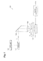
- a laser processing device 100 comprises a laser light source 101 which causes laser light L to oscillate in a pulsating manner, a dichroic mirror 103 arranged such as to change the direction of the optical axis (optical path) of the laser light L by 90°, and a condenser lens 105 for converging the laser light L.
- the laser processing device 100 also comprises a support table 107 for supporting an object to be processed 1 irradiated with the laser light L converged by the condenser lens 105, a stage 111 for moving the support table 107, a laser light source controller 102 for controlling the laser light source 101 in order to regulate the output, pulse width, and the like of the laser light L, and a stage controller 115 for controlling the movement of the stage 111.
- the laser light L emitted from the laser light source 101 changes the direction of its optical axis by 90° with the dichroic mirror 103 and then is converged by the condenser lens 105 into the object 1 mounted on the support table 107.
- the stage 111 is shifted, so that the object 1 moves relative to the laser light L along a part to form a modified region 5. This forms a modified region in the object 1 along the part 5.
- the part 5 is set in the object 1, for which a semiconductor material, a piezoelectric material, or the like is used.
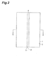
- the part 5 is a virtual line extending straight.
- the laser light L is relatively moved along the part 5 (i.e., in the direction of arrow A in Fig. 2 ) while locating a converging point P within the object 1 as illustrated in Fig. 3 .
- This forms a modified region 7 within the object 1 along the part 5 as illustrated in Figs. 4 to 6 , whereby the modified region 7 becomes a removing region 8 to be removed by etching which will be explained later.
- the converging point P is a position at which the laser light L is converged.
- the part 5 may be curved instead of being straight, shaped into a three-dimensional curved or planar surface form, or specified in terms of coordinates.
- the modified region 7 may be formed either continuously or intermittently.
- the modified region 7 may be formed like lines or dots. It will be sufficient if the modified region 7 is formed at least within the object 1. There are cases where fractures are formed from the modified region 7 acting as a start point, and the fractures and modified region 7 may be exposed at outer surfaces (the front face, rear face, and outer peripheral face) of the object 1.
- the laser light L is absorbed in particular in the vicinity of the converging point within the object 1 while being transmitted therethrough, whereby the modified region 7 is formed in the object 1 (i.e., internal absorption type laser processing).
- the processing region gradually progresses from the front face 3 side to the rear face side in general.
- the modified region 7 in accordance with this embodiment means regions whose physical characteristics such as density, refractive index, and mechanical strength have attained states different from those of their surroundings.
- Examples of the modified region 7 include molten processed regions, crack regions, dielectric breakdown regions, refractive index changed regions, and their mixed regions.
- Further examples of the modified region 7 include an area where the density has changed from that of an unmodified region in a material of the object 1 and an area formed with a lattice defect (which may collectively be referred to as a high-density transitional region).
- the molten processed regions, refractive index changed regions, areas where the modified region has a density different from that of the unmodified region, or areas formed with a lattice defect may further incorporate a fracture (cut or microcrack) therewithin or at an interface between the modified region 7 and an unmodified region.
- the incorporated fracture may be formed over the whole surface of the modified region 7 or in only a part or a plurality of parts thereof. Examples of the object 1 include those containing or constituted by silicon.
- this embodiment forms the object 1 with the modified region 7 and then etches the object 1, so as to advance the etching selectively along fractures (also known as cracks, microcracks, cuts, and the like; hereinafter simply referred to as "fractures") included in or extending from the modified region 7, thereby removing a part extending along the modified region 7 in the object 1.
- fractures also known as cracks, microcracks, cuts, and the like; hereinafter simply referred to as "fractures”
- etching for example, a capillary action or the like is utilized so that fractures included in or extending from the modified region 7 are impregnated with an etchant, so as to advance the etching along fracture surfaces. This advances the etching selectively at a higher etching rate along the fractures in the object 1 and removes them. Also, by utilizing the characteristic feature that the etching rate of the modified region 7 itself is high, the etching is selectively advanced along the modified region 7, so as to remove it.
- etching examples include a case where the object 1 is immersed in the etchant (dipping) and a case where the object 1 is coated with the etchant while being rotated (spin etching).
- the etching herein encompasses isotropic etching and anisotropic etching.
- Fig. 7 is a chart illustrating examples of etchants for use.
- Each etchant is used at a temperature ranging from ambient temperature to about 100°C, which is set appropriately according to a required etching rate or the like.
- the temperature is preferably about 60°C.
- the etchant employable is not limited to liquids but may be in the form of a gel (jelly or semisolid).
- the isotropic etching is applicable to relatively thin objects to be processed (having a thickness of 10 ⁇ m to 100 ⁇ m, for example), so that the etching can advance isotropically independent of the crystal orientation and the modified region.
- the etchant travels through the fracture to wet the inside, so that the whole surface in the thickness direction becomes a start point for the modified region, whereby a chip etched such that its cut surface is depressed into a semicircular form can be taken out.
- the anisotropic etching is applicable not only to relatively thin objects to be processed but also to thick ones (having a thickness of 800 ⁇ m to 100 ⁇ m, for example).
- the etching can be advanced along the modified region. That is, the anisotropic etching herein enables not only the etching of the plane direction in conformity to the crystal orientation, but also the etching independent of the crystal orientation.
- Figs. 8 to 12 are flow diagrams illustrating the laser processing method in accordance with this embodiment.
- this embodiment is a processing method for manufacturing a component (such as an interposer) which electrically connects a semiconductor device and a printed wiring board or flexible substrate to each other, for example, the method forming the object 1 with a plurality of through holes 24 (see Fig. 11 ) and embedding a conductor into the through holes 24, thereby producing a plurality of through-hole electrodes 30 (see Fig. 12 ).
- a component such as an interposer
- the object 1 is a sheet-like silicon substrate transparent to the wavelength (e.g., 1064 nm) of the laser light L with which it is irradiated and has its front face 3 and rear face 21 (main faces) in (100) planes.
- parts to form modified regions 5 are set as being specified by three-dimensional coordinates along the parts corresponding to the through holes 24.
- Each part 5 is set such as to extend in a direction tilted with respect to the thickness direction of the object 1.
- the part 5 here is set such as to extend along a (111) plane of the object 1.
- the thickness direction of the object 1 (irradiation direction of the laser light L) to be the Z direction
- the object 1 is mounted and held on the mount table with the front face 3 side facing up as illustrated in Fig. 8(a) . Then, while locating a converging point of the laser light L (hereinafter simply referred to as "converging point") at a position near the rear face 21 of the object 1 in the Z direction and relatively moving the converging point in the X direction, irradiation with the laser light L (scan) is performed in an on/off manner from the front face 3 side such that a modified region 7 is formed in the part 5.
- converging point a converging point of the laser light L
- modified region 7 is formed exposed to the rear face 21 in the part corresponding to the through hole 24 in the vicinity of the rear face 21 in the object 1.
- the modified region 7 is formed on the rear face 21 side such as to damage the rear face 21 of the object 1.
- spot irradiation is performed with pulsed laser light as the laser light L, the resulting modified region 7 is constituted by modified spots.
- modified region 7 incorporates therein fractures generated from the modified region 7 (ditto in the following modified regions).
- the above-mentioned X-direction scan is repeatedly performed while progressively changing the position of the converging point in the Z direction from the rear face 21 side to the front face 3 side.
- This forms modified regions 7 joining with each other along the part corresponding to the through hole 24 within the object 1. That is, the modified regions 7 tilted with respect to the Z direction along the (111) plane of the object 1 are formed within the object 1.
- the above-mentioned X-direction scan is performed while locating the converging point at the position near the front face 3 of the object 1 in the Z direction.
- This forms a modified region 7 joining with the existing modified region 7 while being exposed to the front face 3 in the part corresponding to the through hole 24 in the vicinity of the front face 3 in the object 1.
- the modified region 7 continuous with the existing modified region 7 is formed on the front face 3 side such as to damage the front face 3 of the object 1.
- the object 1 is put into a furnace having an internal temperature of 1000°C, for example, so as to oxidize its whole surface by wet oxidation.
- the oxide film 22 is a thermally-oxidized film which is highly resistant to alkali etching liquids which are etchants.
- the surfaces of the modified regions 7 exposed to the front face 3 and rear face 21 of the object 1 are not smooth but rough because of their characteristics, whereby many fractures (cracks) included in the modified region 7 are exposed, thus yielding a fuzzy state.
- the object 1 is etched for 60 minutes with KOH at 85°C, for example, employed as an etchant.
- the etchant is caused to infiltrate from the defects 22b of the oxide film 22 into the modified regions 7 and advance selectively along the modified regions 7 and fractures included in the modified regions 7. This selectively removes the inside of the modified regions 7, thereby forming the through hole 24 tilted with respect to the Z direction in conformity to the (111) plane.
- the defects 22b of the oxide film 22 are peeled off and removed when the etching advances.
- Anisotropic etching is performed as the etching in this embodiment, while the (111) plane of the object 1 is harder to etch (exhibits a lower etching rate). Therefore, when the modified regions 7 extend along the (111) plane as in this embodiment, the etching favorably advances along the modified regions 7. Also, the inner face of the through hole 24 becomes a smooth surface with less irregularities, while the cross section of the through hole 24 attains a rectangular (diamond) form.
- the object 1 is oxidized again by wet oxidation.
- This forms an oxide film 26 as an electrically insulating film on the inner face of the through hole 24.
- a conductor 28 is embedded into the through hole 24 as illustrated in Fig. 12(a) , and electrode pads 29 are formed on the outer surfaces 22a of the oxide film 22 on the front face 3 side and rear face 21 side so as to electrically connect with the conductor 28, respectively, as illustrated in Fig. 12(b) , whereby the through-hole electrode 30 is constructed.
- this embodiment performs laser processing for forming the modified region 7 exposed to the rear face 21, the modified regions 7 within the object 1, and the modified region 7 exposed to the front face 3.
- the oxide film 22 is formed on the front face 3 and rear face 21 by oxidation on the whole surface. During this time, the oxide film 22 is inhibited from growing on the exposed modified regions 7, whereby the defects 22b occur.
- the etching advances selectively along the modified regions 7.
- the oxide film 22 can also inhibit the object 1 from reducing the thickness upon etching and keep the surface accuracy in the front face 3 and rear face 21.
- This embodiment can produce the patterned oxide film 22 by a step of oxidizing the whole surface of the object 1 alone, thereby achieving a high accuracy in aligning the oxide film 22 and the object 1 with each other.
- the object 1 is shaped like a sheet having the front face 3 and rear face 21 in (100) planes and thus is easier to etch in the tilted direction of the through hole 24 (i.e., a direction along the (111) plane) by anisotropic etching. Therefore, this embodiment can favorably form the object 1 with the tilted through hole 24.
- this embodiment produces the oxide film 26 as an insulating film on the inner face of the through hole 24. This can reliably secure insulation between the through-hole electrodes 30 adjacent to each other.
- This embodiment produces the oxide film 22 after forming the modified region 7 as mentioned above and thus can inhibit the laser light L from reducing its energy upon passing through the oxide film 22. This effect becomes remarkable when the front face 3 of the object 1 has already been formed with a device, since the device also lowers the energy of the laser light L.
- this embodiment which can form the through-hole electrodes 30 tilted with respect to the Z direction, exhibits the following operations and effects. That is, when attaining a fine wiring pitch, the electrode pad 29 on the front face 3 side and the electrode pad 29 on the rear face 21 side can be connected directly to each other, so as to secure a wiring width sufficiently, thereby preventing the electric resistance from increasing.
- This embodiment can repeatedly perform the X-direction scan while changing the converging point position in the Y direction (laser processing on the XY plane) and repeatedly perform the same while changing the converging point position in the Z direction, so as to form modified regions 7 corresponding to a plurality of through holes 24.
- the method may repeatedly perform the X-direction scan while changing the converging point position in the Z direction (laser processing on the XZ plane) and repeatedly perform the same while changing the converging point position in the Y direction.
- the method may form a modified region 7 corresponding to one through hole 24 by irradiation with the laser light L while appropriately moving the converging point in the X, Y, and Z directions and repeatedly perform the same by the number corresponding to that of through holes 24.
- the laser light entrance surface for forming the modified regions is not limited to the front face 3 of the object 1, but may be the rear face 21 of the object 1.
- the above-mentioned embodiment produces the oxide film 22 as an etch resist film, a nitride film may be formed.
- the etch resist film may be anything as long as it is resistant to the etchant used in the etching.
- the oxide film 22 may be etched separately, so as to remove the defects 22b. This allows the etchant to infiltrate reliably into the modified regions 7 in the etching for the object 1 in a later stage, whereby the through holes 24 can be formed accurately.
- the on/off irradiation with the laser light L in the above-mentioned embodiment may be performed not only by controlling the on/off of the emission of the laser light L, but also by opening/closing a shutter disposed on the optical path of the laser light L or by masking on/off the front face 3 of the object 1, for example.
- the intensity of the laser light L may be controlled between an intensity at a threshold for forming the modified regions 7 (processing threshold) or higher and an intensity lower than the processing threshold.
- the laser processing method of the present invention can form through holes accurately and facilitate the processing.
Landscapes
- Engineering & Computer Science (AREA)
- Physics & Mathematics (AREA)
- Optics & Photonics (AREA)
- Plasma & Fusion (AREA)
- Mechanical Engineering (AREA)
- Chemical & Material Sciences (AREA)
- Chemical Kinetics & Catalysis (AREA)
- General Chemical & Material Sciences (AREA)
- Oil, Petroleum & Natural Gas (AREA)
- Laser Beam Processing (AREA)
- Weting (AREA)
Abstract
Description
- The present invention relates to a laser processing method and, in particular, to a laser processing method for forming an object to be processed with a through hole.
- Known as a conventional laser processing method is one comprising converging laser light at a sheet-like object to be processed so as to form a modified region within the object and then etching the object so as to remove the modified region, thereby forming the object with a through hole along a thickness direction (see, for example, Patent Literature 1).
- Patent Literature 1: Japanese Patent Application Laid-Open No.
2004-351494 - There is a case where the above-mentioned laser processing method patterns an etch resist film, which is resistant to etching, on an outer surface of the object before the etching. That is, the etch resist film is produced so as to cover the whole area of the outer surface of the object. There is a case where the etch resist film is thereafter exposed to light and so forth, so as to form an opening for infiltrating an etchant into the modified region in an area corresponding to a denatured layer in the etch resist film. This can restrain the opening side of the resulting through hole from widening in excess by etching, for example, whereby the through hole can be formed accurately. In this case, however, the processing may become complicated and cumbersome, since the step of patterning by exposure to light or the like is additionally necessary as mentioned above.
- It is therefore an object of the present invention to provide a laser processing method which can accurately form a through hole and facilitate the processing.
- One aspect of the present invention relates to a laser processing method. This laser processing method is a laser processing method of converging laser light into an object to be processed made of silicon so as to form a modified region and etching the object along the modified region so as to form the object with a through hole, the method comprising a laser light converging step of converging the laser light at the object so as to form the modified region along a part corresponding to the through hole in the object; an etch resist film producing step of producing an etch resist film resistant to etching on an outer surface of the object after the laser light converging step; and an etching step of etching the object so as to advance the etching selectively along the modified region and form the through hole after the etch resist film producing step; wherein the laser light converging step exposes the modified region to the outer surface of the object.
- In this laser processing method, when producing the etch resist film, the etch resist film is inhibited from growing on the modified region exposed to the outer surface of the object. Therefore, on the modified region, the etch resist film is not substantially produced or is produced coarser in terms of density than its surroundings, for example, whereby defects may occur in the etch resist film. Hence, in the etching step, an etchant may infiltrate from the defects in the etch resist film into the modified region, thereby advancing the etching selectively along the modified region. As a consequence, when producing the etch resist film on the outer surface, this laser processing method requires no patterning step by exposure to light or the like, thus making it possible to form the through hole accurately and facilitate the processing.
- The object to be processed may be shaped like a sheet having a main face in a (100) plane, the through hole may tilt with respect to the thickness direction of the object, and the etching step may perform anisotropic etching as the etching. This can favorably form the object with the through hole tilted with respect to the thickness direction.
- The method may further comprise a step of removing the etch resist film produced on the exposed modified region by etching the etch resist film after the etch resist film producing step before the etching step. This removes defects in the etch resist film, whereby the etchant can reliably infiltrate into the modified region in the etching step.
- The method may be a laser processing method for forming the object with a plurality of through holes, further comprising an insulating film producing step of producing an insulating film on an inner face of the through holes in the object after the etching step. When forming a plurality of through-hole electrodes by embedding a conductor in each of a plurality of through holes, for example, this can secure insulation between the through-hole electrodes adjacent to each other.
- The laser processing method in accordance with the present invention can accurately form a through hole and facilitate the processing.
-
- [
Fig. 1 ] is a schematic structural diagram of a laser processing device used for forming a modified region; - [
Fig. 2 ] is a plan view of an object to be processed in which the modified region is to be formed; - [
Fig. 3 ] is a sectional view of the object taken along the line III-III ofFig. 2 ; - [
Fig. 4 ] is a plan view of the object after laser processing; - [
Fig. 5 ] is a sectional view of the object taken along the line V-V ofFig. 4 ; - [
Fig. 6 ] is a sectional view of the object taken along the line VI-VI ofFig. 4 ; - [
Fig. 7 ] is a chart illustrating examples of etchants; - [
Fig. 8 ] (a) is a flow diagram explaining the laser processing method in accordance with an embodiment, while (b) is a flow diagram illustrating a stage subsequent toFig. 8(a) ; - [
Fig. 9 ] (a) is a flow diagram illustrating a stage subsequent toFig. 8(b) , while (b) is a flow diagram illustrating a stage subsequent toFig. 9(a) ; - [
Fig. 10 ] is a view enlarging a part of the object inFig. 9(b) ; - [
Fig. 11 ] (a) is a flow diagram illustrating a stage subsequent toFig. 9(b) , while (b) is a flow diagram illustrating a stage subsequent toFig. 11(a) ; and - [
Fig. 12 ] (a) is a flow diagram illustrating a stage subsequent toFig. 11(b) , while (b) is a flow diagram illustrating a stage subsequent toFig. 12(a) . - In the following, preferred embodiments of the present invention will be explained in detail with reference to the drawings. In the following explanations, the same or equivalent constituents will be referred to with the same signs while omitting their overlapping descriptions.
- The laser processing method in accordance with an embodiment converges laser light into an object to be processed, so as to form a modified region. Therefore, the forming of the modified region will firstly be explained in the following with reference to
Figs. 1 to 6 . - As illustrated in
Fig. 1 , alaser processing device 100 comprises alaser light source 101 which causes laser light L to oscillate in a pulsating manner, adichroic mirror 103 arranged such as to change the direction of the optical axis (optical path) of the laser light L by 90°, and acondenser lens 105 for converging the laser light L. Thelaser processing device 100 also comprises a support table 107 for supporting an object to be processed 1 irradiated with the laser light L converged by thecondenser lens 105, astage 111 for moving the support table 107, a laserlight source controller 102 for controlling thelaser light source 101 in order to regulate the output, pulse width, and the like of the laser light L, and astage controller 115 for controlling the movement of thestage 111. - In the
laser processing device 100, the laser light L emitted from thelaser light source 101 changes the direction of its optical axis by 90° with thedichroic mirror 103 and then is converged by thecondenser lens 105 into theobject 1 mounted on the support table 107. At the same time, thestage 111 is shifted, so that theobject 1 moves relative to the laser light L along a part to form a modifiedregion 5. This forms a modified region in theobject 1 along thepart 5. - As illustrated in
Fig. 2 , thepart 5 is set in theobject 1, for which a semiconductor material, a piezoelectric material, or the like is used. Here, thepart 5 is a virtual line extending straight. When forming a modified region within theobject 1, the laser light L is relatively moved along the part 5 (i.e., in the direction of arrow A inFig. 2 ) while locating a converging point P within theobject 1 as illustrated inFig. 3 . This forms a modifiedregion 7 within theobject 1 along thepart 5 as illustrated inFigs. 4 to 6 , whereby the modifiedregion 7 becomes a removingregion 8 to be removed by etching which will be explained later. - The converging point P is a position at which the laser light L is converged. The
part 5 may be curved instead of being straight, shaped into a three-dimensional curved or planar surface form, or specified in terms of coordinates. Themodified region 7 may be formed either continuously or intermittently. Themodified region 7 may be formed like lines or dots. It will be sufficient if the modifiedregion 7 is formed at least within theobject 1. There are cases where fractures are formed from the modifiedregion 7 acting as a start point, and the fractures and modifiedregion 7 may be exposed at outer surfaces (the front face, rear face, and outer peripheral face) of theobject 1. - Here, the laser light L is absorbed in particular in the vicinity of the converging point within the
object 1 while being transmitted therethrough, whereby themodified region 7 is formed in the object 1 (i.e., internal absorption type laser processing). In the case of forming a removing part such as a hole or groove by melting it away from the front face 3 (surface absorption type laser processing), the processing region gradually progresses from thefront face 3 side to the rear face side in general. - The modified
region 7 in accordance with this embodiment means regions whose physical characteristics such as density, refractive index, and mechanical strength have attained states different from those of their surroundings. Examples of the modifiedregion 7 include molten processed regions, crack regions, dielectric breakdown regions, refractive index changed regions, and their mixed regions. Further examples of the modifiedregion 7 include an area where the density has changed from that of an unmodified region in a material of theobject 1 and an area formed with a lattice defect (which may collectively be referred to as a high-density transitional region). - The molten processed regions, refractive index changed regions, areas where the modified region has a density different from that of the unmodified region, or areas formed with a lattice defect may further incorporate a fracture (cut or microcrack) therewithin or at an interface between the modified
region 7 and an unmodified region. The incorporated fracture may be formed over the whole surface of the modifiedregion 7 or in only a part or a plurality of parts thereof. Examples of theobject 1 include those containing or constituted by silicon. - Here, this embodiment forms the
object 1 with the modifiedregion 7 and then etches theobject 1, so as to advance the etching selectively along fractures (also known as cracks, microcracks, cuts, and the like; hereinafter simply referred to as "fractures") included in or extending from the modifiedregion 7, thereby removing a part extending along the modifiedregion 7 in theobject 1. - In the etching in this embodiment, for example, a capillary action or the like is utilized so that fractures included in or extending from the modified
region 7 are impregnated with an etchant, so as to advance the etching along fracture surfaces. This advances the etching selectively at a higher etching rate along the fractures in theobject 1 and removes them. Also, by utilizing the characteristic feature that the etching rate of the modifiedregion 7 itself is high, the etching is selectively advanced along the modifiedregion 7, so as to remove it. - Examples of the etching include a case where the
object 1 is immersed in the etchant (dipping) and a case where theobject 1 is coated with the etchant while being rotated (spin etching). The etching herein encompasses isotropic etching and anisotropic etching. -
Fig. 7 is a chart illustrating examples of etchants for use. Each etchant is used at a temperature ranging from ambient temperature to about 100°C, which is set appropriately according to a required etching rate or the like. When etching Si (anisotropic) with KOH, for example, the temperature is preferably about 60°C. The etchant employable is not limited to liquids but may be in the form of a gel (jelly or semisolid). - The isotropic etching is applicable to relatively thin objects to be processed (having a thickness of 10 µm to 100 µm, for example), so that the etching can advance isotropically independent of the crystal orientation and the modified region. When a fracture is exposed to the front face in this case, the etchant travels through the fracture to wet the inside, so that the whole surface in the thickness direction becomes a start point for the modified region, whereby a chip etched such that its cut surface is depressed into a semicircular form can be taken out. On the other hand, the anisotropic etching is applicable not only to relatively thin objects to be processed but also to thick ones (having a thickness of 800 µm to 100 µm, for example). In this case, even when the surface to be formed with the modified region differs from its plane direction, the etching can be advanced along the modified region. That is, the anisotropic etching herein enables not only the etching of the plane direction in conformity to the crystal orientation, but also the etching independent of the crystal orientation.
- The laser processing method in accordance with an embodiment of the present invention will now be explained in detail.
Figs. 8 to 12 are flow diagrams illustrating the laser processing method in accordance with this embodiment. - As illustrated in
Figs. 8 to 12 , this embodiment is a processing method for manufacturing a component (such as an interposer) which electrically connects a semiconductor device and a printed wiring board or flexible substrate to each other, for example, the method forming theobject 1 with a plurality of through holes 24 (seeFig. 11 ) and embedding a conductor into the throughholes 24, thereby producing a plurality of through-hole electrodes 30 (seeFig. 12 ). - As illustrated in
Fig. 8(a) , theobject 1 is a sheet-like silicon substrate transparent to the wavelength (e.g., 1064 nm) of the laser light L with which it is irradiated and has itsfront face 3 and rear face 21 (main faces) in (100) planes. In theobject 1, parts to form modifiedregions 5 are set as being specified by three-dimensional coordinates along the parts corresponding to the through holes 24. Eachpart 5 is set such as to extend in a direction tilted with respect to the thickness direction of theobject 1. Thepart 5 here is set such as to extend along a (111) plane of theobject 1. - The following explanation will assume the thickness direction of the object 1 (irradiation direction of the laser light L) to be the Z direction, a direction to which the parts 5 (through holes 24) tilt with respect to the thickness direction to be the X direction, and a direction perpendicular to the X and Z directions to be the Y direction.
- First, when processing the
object 1 in this embodiment, theobject 1 is mounted and held on the mount table with thefront face 3 side facing up as illustrated inFig. 8(a) . Then, while locating a converging point of the laser light L (hereinafter simply referred to as "converging point") at a position near therear face 21 of theobject 1 in the Z direction and relatively moving the converging point in the X direction, irradiation with the laser light L (scan) is performed in an on/off manner from thefront face 3 side such that a modifiedregion 7 is formed in thepart 5. - This forms the modified
region 7 exposed to therear face 21 in the part corresponding to the throughhole 24 in the vicinity of therear face 21 in theobject 1. In other words, the modifiedregion 7 is formed on therear face 21 side such as to damage therear face 21 of theobject 1. Here, since spot irradiation is performed with pulsed laser light as the laser light L, the resulting modifiedregion 7 is constituted by modified spots. Thus formed modifiedregion 7 incorporates therein fractures generated from the modified region 7 (ditto in the following modified regions). - Subsequently, as illustrated in
Fig. 8(b) , the position of the converging point is shifted in the Z direction toward thefront face 3, and then the above-mentioned X-direction scan is performed. This newly forms a modifiedregion 7 joining with the existing modifiedregion 7 in the part corresponding to the throughhole 24 at the position closer to thefront face 3 than is the existing modifiedregion 7 in the Z direction. - Then, the above-mentioned X-direction scan is repeatedly performed while progressively changing the position of the converging point in the Z direction from the
rear face 21 side to thefront face 3 side. This forms modifiedregions 7 joining with each other along the part corresponding to the throughhole 24 within theobject 1. That is, the modifiedregions 7 tilted with respect to the Z direction along the (111) plane of theobject 1 are formed within theobject 1. - Thereafter, as illustrated in
Fig. 9(a) , the above-mentioned X-direction scan is performed while locating the converging point at the position near thefront face 3 of theobject 1 in the Z direction. This forms a modifiedregion 7 joining with the existing modifiedregion 7 while being exposed to thefront face 3 in the part corresponding to the throughhole 24 in the vicinity of thefront face 3 in theobject 1. In other words, the modifiedregion 7 continuous with the existing modifiedregion 7 is formed on thefront face 3 side such as to damage thefront face 3 of theobject 1. - Next, as illustrated in
Fig. 9(b) , theobject 1 is put into a furnace having an internal temperature of 1000°C, for example, so as to oxidize its whole surface by wet oxidation. This forms anoxide film 22 as an etch resist film resistant to etching on outer surfaces (at least thefront face 3 and rear face 21) of the object. Here, theoxide film 22 is a thermally-oxidized film which is highly resistant to alkali etching liquids which are etchants. - Here, as illustrated in
Fig. 10 , the surfaces of the modifiedregions 7 exposed to thefront face 3 andrear face 21 of theobject 1 are not smooth but rough because of their characteristics, whereby many fractures (cracks) included in the modifiedregion 7 are exposed, thus yielding a fuzzy state. This inhibits theoxide film 22 from growing when producing the same (seeFig. 9(b) ), thereby causing an error in forming theoxide film 22. Therefore, theoxide film 22 is not substantially produced on this modifiedregion 7 or is produced coarser in terms of density than its surroundings, wherebydefects 22b occur in theoxide film 22. - Subsequently, as illustrated in
Fig. 11(a) , theobject 1 is etched for 60 minutes with KOH at 85°C, for example, employed as an etchant. Specifically, the etchant is caused to infiltrate from thedefects 22b of theoxide film 22 into the modifiedregions 7 and advance selectively along the modifiedregions 7 and fractures included in the modifiedregions 7. This selectively removes the inside of the modifiedregions 7, thereby forming the throughhole 24 tilted with respect to the Z direction in conformity to the (111) plane. Thedefects 22b of theoxide film 22 are peeled off and removed when the etching advances. - Anisotropic etching is performed as the etching in this embodiment, while the (111) plane of the
object 1 is harder to etch (exhibits a lower etching rate). Therefore, when the modifiedregions 7 extend along the (111) plane as in this embodiment, the etching favorably advances along the modifiedregions 7. Also, the inner face of the throughhole 24 becomes a smooth surface with less irregularities, while the cross section of the throughhole 24 attains a rectangular (diamond) form. - Next, as illustrated in
Fig. 11(b) , theobject 1 is oxidized again by wet oxidation. This forms anoxide film 26 as an electrically insulating film on the inner face of the throughhole 24. Thereafter, aconductor 28 is embedded into the throughhole 24 as illustrated inFig. 12(a) , andelectrode pads 29 are formed on theouter surfaces 22a of theoxide film 22 on thefront face 3 side andrear face 21 side so as to electrically connect with theconductor 28, respectively, as illustrated inFig. 12(b) , whereby the through-hole electrode 30 is constructed. - As in the foregoing, this embodiment performs laser processing for forming the modified
region 7 exposed to therear face 21, the modifiedregions 7 within theobject 1, and the modifiedregion 7 exposed to thefront face 3. Here, theoxide film 22 is formed on thefront face 3 andrear face 21 by oxidation on the whole surface. During this time, theoxide film 22 is inhibited from growing on the exposed modifiedregions 7, whereby thedefects 22b occur. Hence, in the subsequent etching, while the etchant reliably enters from thedefects 22b of theoxide film 22 as base points, the etching advances selectively along the modifiedregions 7. - Therefore, a conventional step of patterning by exposure to light or the like is unnecessary in this embodiment for forming the
oxide film 22 on thefront face 3 andrear face 21 of theobject 1, whereby the throughhole 24 can be formed accurately, while the processing can be facilitated. This can further restrain the opening side of the throughhole 24 from widening and the modifiedregion 7 from being etched in excess and thereby increasing the cross-sectional area of the throughhole 24 and so forth, whereby the form and size of the throughhole 24 can be controlled favorably. Theoxide film 22 can also inhibit theobject 1 from reducing the thickness upon etching and keep the surface accuracy in thefront face 3 andrear face 21. - This embodiment can produce the patterned
oxide film 22 by a step of oxidizing the whole surface of theobject 1 alone, thereby achieving a high accuracy in aligning theoxide film 22 and theobject 1 with each other. - In this embodiment, as mentioned above, the
object 1 is shaped like a sheet having thefront face 3 andrear face 21 in (100) planes and thus is easier to etch in the tilted direction of the through hole 24 (i.e., a direction along the (111) plane) by anisotropic etching. Therefore, this embodiment can favorably form theobject 1 with the tilted throughhole 24. - As mentioned above, this embodiment produces the
oxide film 26 as an insulating film on the inner face of the throughhole 24. This can reliably secure insulation between the through-hole electrodes 30 adjacent to each other. - This embodiment produces the
oxide film 22 after forming the modifiedregion 7 as mentioned above and thus can inhibit the laser light L from reducing its energy upon passing through theoxide film 22. This effect becomes remarkable when thefront face 3 of theobject 1 has already been formed with a device, since the device also lowers the energy of the laser light L. - Recently, as integration has been becoming higher, there have been stronger demands for developing interposers having fine wiring pitches. In this regard, this embodiment, which can form the through-
hole electrodes 30 tilted with respect to the Z direction, exhibits the following operations and effects. That is, when attaining a fine wiring pitch, theelectrode pad 29 on thefront face 3 side and theelectrode pad 29 on therear face 21 side can be connected directly to each other, so as to secure a wiring width sufficiently, thereby preventing the electric resistance from increasing. - This embodiment can repeatedly perform the X-direction scan while changing the converging point position in the Y direction (laser processing on the XY plane) and repeatedly perform the same while changing the converging point position in the Z direction, so as to form modified
regions 7 corresponding to a plurality of throughholes 24. The method may repeatedly perform the X-direction scan while changing the converging point position in the Z direction (laser processing on the XZ plane) and repeatedly perform the same while changing the converging point position in the Y direction. The method may form a modifiedregion 7 corresponding to one throughhole 24 by irradiation with the laser light L while appropriately moving the converging point in the X, Y, and Z directions and repeatedly perform the same by the number corresponding to that of throughholes 24. - Though a preferred embodiment of the present invention has been explained in the foregoing, the present invention is not limited thereto but may be modified or applied to others within the scope not changing the gist recited in each claim.
- For example, the laser light entrance surface for forming the modified regions is not limited to the
front face 3 of theobject 1, but may be therear face 21 of theobject 1. Though the above-mentioned embodiment produces theoxide film 22 as an etch resist film, a nitride film may be formed. The etch resist film may be anything as long as it is resistant to the etchant used in the etching. - After producing the
oxide film 22 before etching, theoxide film 22 may be etched separately, so as to remove thedefects 22b. This allows the etchant to infiltrate reliably into the modifiedregions 7 in the etching for theobject 1 in a later stage, whereby the throughholes 24 can be formed accurately. - The on/off irradiation with the laser light L in the above-mentioned embodiment may be performed not only by controlling the on/off of the emission of the laser light L, but also by opening/closing a shutter disposed on the optical path of the laser light L or by masking on/off the
front face 3 of theobject 1, for example. Further, the intensity of the laser light L may be controlled between an intensity at a threshold for forming the modified regions 7 (processing threshold) or higher and an intensity lower than the processing threshold. - The laser processing method of the present invention can form through holes accurately and facilitate the processing.
- 1...objects to be processed; 3...front face (outer surface; main face); 7...modified region; 21...rear face (outer surface; main face); 22... oxide film (etch resist film); 24... through hole; 26 ... oxide film (insulating film); L...laser light; P...converging point
Claims (4)
- A laser processing method of converging laser light into an object to be processed made of silicon so as to form a modified region and etching the object along the modified region so as to form the object with a through hole, the method comprising:a laser light converging step of converging the laser light at the object so as to form the modified region along a part corresponding to the through hole in the object;an etch resist film producing step of producing an etch resist film resistant to etching on an outer surface of the object after the laser light converging step; andan etching step of etching the object so as to advance the etching selectively along the modified region and form the through hole after the etch resist film producing step;wherein the laser light converging step exposes the modified region to the outer surface of the object.
- A laser processing method according to claim 1, wherein the object is shaped like a sheet having a main face in a (100) plane;
wherein the through hole tilts with respect to the thickness direction of the object; and
wherein the etching step performs anisotropic etching as the etching. - A laser processing method according to claim 1 or 2, further comprising a step of removing the etch resist film produced on the exposed modified region by etching the etch resist film after the etch resist film producing step before the etching step.
- A laser processing method according to one of claims 1 to 3 for forming the object with a plurality of through holes,
the method further comprising an insulating film producing step of producing an insulating film on an inner face of the through holes in the object after the etching step.
Applications Claiming Priority (2)
| Application Number | Priority Date | Filing Date | Title |
|---|---|---|---|
| JP2010167426A JP5702556B2 (en) | 2010-07-26 | 2010-07-26 | Laser processing method |
| PCT/JP2011/066322 WO2012014711A1 (en) | 2010-07-26 | 2011-07-19 | Laser processing method |
Publications (3)
| Publication Number | Publication Date |
|---|---|
| EP2600392A1 true EP2600392A1 (en) | 2013-06-05 |
| EP2600392A4 EP2600392A4 (en) | 2016-12-14 |
| EP2600392B1 EP2600392B1 (en) | 2019-12-11 |
Family
ID=45529927
Family Applications (1)
| Application Number | Title | Priority Date | Filing Date |
|---|---|---|---|
| EP11812303.3A Active EP2600392B1 (en) | 2010-07-26 | 2011-07-19 | Laser processing method |
Country Status (7)
| Country | Link |
|---|---|
| US (1) | US8685269B2 (en) |
| EP (1) | EP2600392B1 (en) |
| JP (1) | JP5702556B2 (en) |
| KR (1) | KR20130088147A (en) |
| CN (1) | CN103026470B (en) |
| TW (1) | TWI536441B (en) |
| WO (1) | WO2012014711A1 (en) |
Families Citing this family (1)
| Publication number | Priority date | Publication date | Assignee | Title |
|---|---|---|---|---|
| JP7063543B2 (en) * | 2017-04-17 | 2022-05-09 | 浜松ホトニクス株式会社 | How to cut the object to be machined |
Family Cites Families (41)
| Publication number | Priority date | Publication date | Assignee | Title |
|---|---|---|---|---|
| JPH04150212A (en) | 1990-10-09 | 1992-05-22 | Seiko Epson Corp | Etching method for crystal substrate |
| JPH0740482A (en) | 1993-07-27 | 1995-02-10 | Jsp Corp | Expanded polypropylene resin laminate and method for producing the laminate |
| JP2873937B2 (en) | 1996-05-24 | 1999-03-24 | 工業技術院長 | Optical microfabrication method for glass |
| JP3473668B2 (en) | 1997-01-23 | 2003-12-08 | セイコーエプソン株式会社 | Ink jet recording head |
| KR100379350B1 (en) * | 1998-12-16 | 2003-04-08 | 세이코 엡슨 가부시키가이샤 | Semiconductor chip, semiconductor device, circuit board and electronic equipment and production methods for them |
| JP4497147B2 (en) | 1998-12-16 | 2010-07-07 | セイコーエプソン株式会社 | Semiconductor chip manufacturing method, semiconductor device manufacturing method, circuit board manufacturing method, and electronic device manufacturing method |
| US6563079B1 (en) | 1999-02-25 | 2003-05-13 | Seiko Epson Corporation | Method for machining work by laser beam |
| JP2000246475A (en) * | 1999-02-25 | 2000-09-12 | Seiko Epson Corp | Processing method by laser beam |
| JP4659300B2 (en) | 2000-09-13 | 2011-03-30 | 浜松ホトニクス株式会社 | Laser processing method and semiconductor chip manufacturing method |
| JP4880820B2 (en) | 2001-01-19 | 2012-02-22 | 株式会社レーザーシステム | Laser assisted machining method |
| AU2003211763A1 (en) | 2002-03-12 | 2003-09-22 | Hamamatsu Photonics K.K. | Method for dicing substrate |
| CA2428187C (en) | 2002-05-08 | 2012-10-02 | National Research Council Of Canada | Method of fabricating sub-micron structures in transparent dielectric materials |
| JP4150212B2 (en) | 2002-05-17 | 2008-09-17 | パナソニック コミュニケーションズ株式会社 | Printing system |
| JP4329374B2 (en) | 2002-07-29 | 2009-09-09 | パナソニック電工株式会社 | LIGHT EMITTING ELEMENT AND MANUFACTURING METHOD THEREOF |
| JP4158481B2 (en) | 2002-10-21 | 2008-10-01 | セイコーエプソン株式会社 | Laser processing method and apparatus, and drilling method using the apparatus |
| JP2004160618A (en) | 2002-11-15 | 2004-06-10 | Seiko Epson Corp | Micromachine and method of manufacturing micromachine |
| JP2004223586A (en) | 2003-01-24 | 2004-08-12 | Institute Of Physical & Chemical Research | Processing method inside transparent material |
| JP2004304130A (en) | 2003-04-01 | 2004-10-28 | Seiko Epson Corp | Method for manufacturing semiconductor device |
| JP2004351494A (en) * | 2003-05-30 | 2004-12-16 | Seiko Epson Corp | Drilling method of material transparent to laser |
| JP2004359475A (en) | 2003-06-02 | 2004-12-24 | Seiko Epson Corp | Method for manufacturing optical element and optical device |
| JP4385656B2 (en) | 2003-06-11 | 2009-12-16 | セイコーエプソン株式会社 | Liquid ejecting head and manufacturing method thereof |
| JP4182841B2 (en) | 2003-08-28 | 2008-11-19 | セイコーエプソン株式会社 | Single crystal substrate processing method |
| JP2005121916A (en) | 2003-10-16 | 2005-05-12 | Seiko Epson Corp | Method for manufacturing substrate with recess for lenticular lens, substrate with recess for lenticular lens, lenticular lens substrate, transmissive screen and rear projector |
| JP2005121915A (en) | 2003-10-16 | 2005-05-12 | Seiko Epson Corp | Manufacturing method of substrate with recess for microlens, substrate with recess for microlens, microlens substrate, counter substrate for liquid crystal panel, liquid crystal panel, and projection display device |
| JP2005144586A (en) | 2003-11-13 | 2005-06-09 | Seiko Epson Corp | Structure manufacturing method, droplet discharge head, and droplet discharge apparatus |
| JP2005144622A (en) | 2003-11-18 | 2005-06-09 | Seiko Epson Corp | Structure manufacturing method, droplet discharge head, and droplet discharge apparatus |
| JP2005152693A (en) | 2003-11-20 | 2005-06-16 | Seiko Epson Corp | Method for manufacturing structure body, liquid drop delivery head and liquid drop delivery device |
| JP2005169993A (en) | 2003-12-15 | 2005-06-30 | Canon Inc | Ink jet recording head and method of manufacturing ink jet recording head |
| JP2005208175A (en) | 2004-01-20 | 2005-08-04 | Seiko Epson Corp | OPTICAL COMPONENT AND METHOD FOR MANUFACTURING THE SAME, OPTICAL MODULE, OPTICAL COMMUNICATION DEVICE, ELECTRONIC DEVICE |
| JP2005206401A (en) * | 2004-01-21 | 2005-08-04 | Seiko Epson Corp | Structure manufacturing method, droplet discharge head, and droplet discharge apparatus |
| JP2005306702A (en) | 2004-04-26 | 2005-11-04 | Namiki Precision Jewel Co Ltd | Method for forming a microhole having a tapered shape |
| JP2005351774A (en) | 2004-06-10 | 2005-12-22 | Seiko Epson Corp | Microarray manufacturing head manufacturing method, microarray manufacturing head, and microarray manufacturing apparatus |
| JP4630971B2 (en) | 2004-12-21 | 2011-02-09 | 並木精密宝石株式会社 | Microstructure formation method using pulsed laser |
| JP2006290630A (en) | 2005-02-23 | 2006-10-26 | Nippon Sheet Glass Co Ltd | Processing method of glass using laser |
| JP2007036758A (en) | 2005-07-27 | 2007-02-08 | Seiko Epson Corp | AT-cut crystal resonator element, method for manufacturing the same, and crystal device |
| JP4564434B2 (en) * | 2005-09-30 | 2010-10-20 | Okiセミコンダクタ株式会社 | Semiconductor device and manufacturing method of semiconductor device |
| JP2007101833A (en) | 2005-10-04 | 2007-04-19 | Seiko Epson Corp | Microlens manufacturing method, microlens, spatial light modulator, screen and projector |
| WO2008146744A1 (en) | 2007-05-25 | 2008-12-04 | Hamamatsu Photonics K.K. | Working method for cutting |
| JP4902472B2 (en) * | 2007-09-18 | 2012-03-21 | 三洋電機株式会社 | Solar cell and solar cell module |
| JP4964186B2 (en) * | 2008-04-28 | 2012-06-27 | 三菱電機株式会社 | Method for manufacturing photovoltaic device |
| JP2010142837A (en) * | 2008-12-18 | 2010-07-01 | Seiko Epson Corp | Laser processing method |
-
2010
- 2010-07-26 JP JP2010167426A patent/JP5702556B2/en not_active Expired - Fee Related
-
2011
- 2011-07-19 EP EP11812303.3A patent/EP2600392B1/en active Active
- 2011-07-19 CN CN201180036527.4A patent/CN103026470B/en not_active Expired - Fee Related
- 2011-07-19 WO PCT/JP2011/066322 patent/WO2012014711A1/en not_active Ceased
- 2011-07-19 KR KR1020137004728A patent/KR20130088147A/en not_active Ceased
- 2011-07-19 US US13/388,717 patent/US8685269B2/en not_active Expired - Fee Related
- 2011-07-26 TW TW100126367A patent/TWI536441B/en not_active IP Right Cessation
Also Published As
| Publication number | Publication date |
|---|---|
| JP5702556B2 (en) | 2015-04-15 |
| JP2012028645A (en) | 2012-02-09 |
| CN103026470B (en) | 2016-08-03 |
| EP2600392B1 (en) | 2019-12-11 |
| TWI536441B (en) | 2016-06-01 |
| CN103026470A (en) | 2013-04-03 |
| KR20130088147A (en) | 2013-08-07 |
| US20120129348A1 (en) | 2012-05-24 |
| TW201234471A (en) | 2012-08-16 |
| EP2600392A4 (en) | 2016-12-14 |
| WO2012014711A1 (en) | 2012-02-02 |
| US8685269B2 (en) | 2014-04-01 |
Similar Documents
| Publication | Publication Date | Title |
|---|---|---|
| EP2599581B1 (en) | Laser processing method | |
| EP2600397B1 (en) | Method for manufacturing interposer | |
| US8802544B2 (en) | Method for manufacturing chip including a functional device formed on a substrate | |
| US8673167B2 (en) | Laser processing method | |
| EP2599578B1 (en) | Laser processing method for fabricating a through hole | |
| EP2600392B1 (en) | Laser processing method |
Legal Events
| Date | Code | Title | Description |
|---|---|---|---|
| PUAI | Public reference made under article 153(3) epc to a published international application that has entered the european phase |
Free format text: ORIGINAL CODE: 0009012 |
|
| 17P | Request for examination filed |
Effective date: 20130222 |
|
| AK | Designated contracting states |
Kind code of ref document: A1 Designated state(s): AL AT BE BG CH CY CZ DE DK EE ES FI FR GB GR HR HU IE IS IT LI LT LU LV MC MK MT NL NO PL PT RO RS SE SI SK SM TR |
|
| DAX | Request for extension of the european patent (deleted) | ||
| RA4 | Supplementary search report drawn up and despatched (corrected) |
Effective date: 20161116 |
|
| RIC1 | Information provided on ipc code assigned before grant |
Ipc: B23K 26/38 20140101ALN20161110BHEP Ipc: B23K 26/00 20140101ALN20161110BHEP Ipc: H01L 21/306 20060101AFI20161110BHEP |
|
| STAA | Information on the status of an ep patent application or granted ep patent |
Free format text: STATUS: EXAMINATION IS IN PROGRESS |
|
| 17Q | First examination report despatched |
Effective date: 20180308 |
|
| GRAP | Despatch of communication of intention to grant a patent |
Free format text: ORIGINAL CODE: EPIDOSNIGR1 |
|
| STAA | Information on the status of an ep patent application or granted ep patent |
Free format text: STATUS: GRANT OF PATENT IS INTENDED |
|
| RIC1 | Information provided on ipc code assigned before grant |
Ipc: B23K 26/00 20140101ALN20190529BHEP Ipc: H01L 21/306 20060101AFI20190529BHEP Ipc: B23K 26/38 20140101ALN20190529BHEP |
|
| INTG | Intention to grant announced |
Effective date: 20190619 |
|
| GRAS | Grant fee paid |
Free format text: ORIGINAL CODE: EPIDOSNIGR3 |
|
| GRAA | (expected) grant |
Free format text: ORIGINAL CODE: 0009210 |
|
| STAA | Information on the status of an ep patent application or granted ep patent |
Free format text: STATUS: THE PATENT HAS BEEN GRANTED |
|
| AK | Designated contracting states |
Kind code of ref document: B1 Designated state(s): AL AT BE BG CH CY CZ DE DK EE ES FI FR GB GR HR HU IE IS IT LI LT LU LV MC MK MT NL NO PL PT RO RS SE SI SK SM TR |
|
| REG | Reference to a national code |
Ref country code: GB Ref legal event code: FG4D |
|
| REG | Reference to a national code |
Ref country code: CH Ref legal event code: EP |
|
| REG | Reference to a national code |
Ref country code: AT Ref legal event code: REF Ref document number: 1213036 Country of ref document: AT Kind code of ref document: T Effective date: 20191215 |
|
| REG | Reference to a national code |
Ref country code: DE Ref legal event code: R096 Ref document number: 602011063984 Country of ref document: DE |
|
| REG | Reference to a national code |
Ref country code: IE Ref legal event code: FG4D |
|
| REG | Reference to a national code |
Ref country code: NL Ref legal event code: MP Effective date: 20191211 |
|
| REG | Reference to a national code |
Ref country code: LT Ref legal event code: MG4D |
|
| PG25 | Lapsed in a contracting state [announced via postgrant information from national office to epo] |
Ref country code: ES Free format text: LAPSE BECAUSE OF FAILURE TO SUBMIT A TRANSLATION OF THE DESCRIPTION OR TO PAY THE FEE WITHIN THE PRESCRIBED TIME-LIMIT Effective date: 20191211 Ref country code: NO Free format text: LAPSE BECAUSE OF FAILURE TO SUBMIT A TRANSLATION OF THE DESCRIPTION OR TO PAY THE FEE WITHIN THE PRESCRIBED TIME-LIMIT Effective date: 20200311 Ref country code: GR Free format text: LAPSE BECAUSE OF FAILURE TO SUBMIT A TRANSLATION OF THE DESCRIPTION OR TO PAY THE FEE WITHIN THE PRESCRIBED TIME-LIMIT Effective date: 20200312 Ref country code: LT Free format text: LAPSE BECAUSE OF FAILURE TO SUBMIT A TRANSLATION OF THE DESCRIPTION OR TO PAY THE FEE WITHIN THE PRESCRIBED TIME-LIMIT Effective date: 20191211 Ref country code: SE Free format text: LAPSE BECAUSE OF FAILURE TO SUBMIT A TRANSLATION OF THE DESCRIPTION OR TO PAY THE FEE WITHIN THE PRESCRIBED TIME-LIMIT Effective date: 20191211 Ref country code: LV Free format text: LAPSE BECAUSE OF FAILURE TO SUBMIT A TRANSLATION OF THE DESCRIPTION OR TO PAY THE FEE WITHIN THE PRESCRIBED TIME-LIMIT Effective date: 20191211 Ref country code: FI Free format text: LAPSE BECAUSE OF FAILURE TO SUBMIT A TRANSLATION OF THE DESCRIPTION OR TO PAY THE FEE WITHIN THE PRESCRIBED TIME-LIMIT Effective date: 20191211 Ref country code: BG Free format text: LAPSE BECAUSE OF FAILURE TO SUBMIT A TRANSLATION OF THE DESCRIPTION OR TO PAY THE FEE WITHIN THE PRESCRIBED TIME-LIMIT Effective date: 20200311 |
|
| PG25 | Lapsed in a contracting state [announced via postgrant information from national office to epo] |
Ref country code: RS Free format text: LAPSE BECAUSE OF FAILURE TO SUBMIT A TRANSLATION OF THE DESCRIPTION OR TO PAY THE FEE WITHIN THE PRESCRIBED TIME-LIMIT Effective date: 20191211 Ref country code: HR Free format text: LAPSE BECAUSE OF FAILURE TO SUBMIT A TRANSLATION OF THE DESCRIPTION OR TO PAY THE FEE WITHIN THE PRESCRIBED TIME-LIMIT Effective date: 20191211 |
|
| PG25 | Lapsed in a contracting state [announced via postgrant information from national office to epo] |
Ref country code: AL Free format text: LAPSE BECAUSE OF FAILURE TO SUBMIT A TRANSLATION OF THE DESCRIPTION OR TO PAY THE FEE WITHIN THE PRESCRIBED TIME-LIMIT Effective date: 20191211 |
|
| PG25 | Lapsed in a contracting state [announced via postgrant information from national office to epo] |
Ref country code: EE Free format text: LAPSE BECAUSE OF FAILURE TO SUBMIT A TRANSLATION OF THE DESCRIPTION OR TO PAY THE FEE WITHIN THE PRESCRIBED TIME-LIMIT Effective date: 20191211 Ref country code: PT Free format text: LAPSE BECAUSE OF FAILURE TO SUBMIT A TRANSLATION OF THE DESCRIPTION OR TO PAY THE FEE WITHIN THE PRESCRIBED TIME-LIMIT Effective date: 20200506 Ref country code: NL Free format text: LAPSE BECAUSE OF FAILURE TO SUBMIT A TRANSLATION OF THE DESCRIPTION OR TO PAY THE FEE WITHIN THE PRESCRIBED TIME-LIMIT Effective date: 20191211 Ref country code: RO Free format text: LAPSE BECAUSE OF FAILURE TO SUBMIT A TRANSLATION OF THE DESCRIPTION OR TO PAY THE FEE WITHIN THE PRESCRIBED TIME-LIMIT Effective date: 20191211 Ref country code: CZ Free format text: LAPSE BECAUSE OF FAILURE TO SUBMIT A TRANSLATION OF THE DESCRIPTION OR TO PAY THE FEE WITHIN THE PRESCRIBED TIME-LIMIT Effective date: 20191211 |
|
| PG25 | Lapsed in a contracting state [announced via postgrant information from national office to epo] |
Ref country code: SM Free format text: LAPSE BECAUSE OF FAILURE TO SUBMIT A TRANSLATION OF THE DESCRIPTION OR TO PAY THE FEE WITHIN THE PRESCRIBED TIME-LIMIT Effective date: 20191211 Ref country code: SK Free format text: LAPSE BECAUSE OF FAILURE TO SUBMIT A TRANSLATION OF THE DESCRIPTION OR TO PAY THE FEE WITHIN THE PRESCRIBED TIME-LIMIT Effective date: 20191211 Ref country code: IS Free format text: LAPSE BECAUSE OF FAILURE TO SUBMIT A TRANSLATION OF THE DESCRIPTION OR TO PAY THE FEE WITHIN THE PRESCRIBED TIME-LIMIT Effective date: 20200411 |
|
| REG | Reference to a national code |
Ref country code: DE Ref legal event code: R097 Ref document number: 602011063984 Country of ref document: DE |
|
| REG | Reference to a national code |
Ref country code: AT Ref legal event code: MK05 Ref document number: 1213036 Country of ref document: AT Kind code of ref document: T Effective date: 20191211 |
|
| PLBE | No opposition filed within time limit |
Free format text: ORIGINAL CODE: 0009261 |
|
| STAA | Information on the status of an ep patent application or granted ep patent |
Free format text: STATUS: NO OPPOSITION FILED WITHIN TIME LIMIT |
|
| PG25 | Lapsed in a contracting state [announced via postgrant information from national office to epo] |
Ref country code: DK Free format text: LAPSE BECAUSE OF FAILURE TO SUBMIT A TRANSLATION OF THE DESCRIPTION OR TO PAY THE FEE WITHIN THE PRESCRIBED TIME-LIMIT Effective date: 20191211 |
|
| 26N | No opposition filed |
Effective date: 20200914 |
|
| PG25 | Lapsed in a contracting state [announced via postgrant information from national office to epo] |
Ref country code: SI Free format text: LAPSE BECAUSE OF FAILURE TO SUBMIT A TRANSLATION OF THE DESCRIPTION OR TO PAY THE FEE WITHIN THE PRESCRIBED TIME-LIMIT Effective date: 20191211 Ref country code: PL Free format text: LAPSE BECAUSE OF FAILURE TO SUBMIT A TRANSLATION OF THE DESCRIPTION OR TO PAY THE FEE WITHIN THE PRESCRIBED TIME-LIMIT Effective date: 20191211 Ref country code: AT Free format text: LAPSE BECAUSE OF FAILURE TO SUBMIT A TRANSLATION OF THE DESCRIPTION OR TO PAY THE FEE WITHIN THE PRESCRIBED TIME-LIMIT Effective date: 20191211 |
|
| PG25 | Lapsed in a contracting state [announced via postgrant information from national office to epo] |
Ref country code: IT Free format text: LAPSE BECAUSE OF FAILURE TO SUBMIT A TRANSLATION OF THE DESCRIPTION OR TO PAY THE FEE WITHIN THE PRESCRIBED TIME-LIMIT Effective date: 20191211 |
|
| REG | Reference to a national code |
Ref country code: DE Ref legal event code: R119 Ref document number: 602011063984 Country of ref document: DE |
|
| PG25 | Lapsed in a contracting state [announced via postgrant information from national office to epo] |
Ref country code: MC Free format text: LAPSE BECAUSE OF FAILURE TO SUBMIT A TRANSLATION OF THE DESCRIPTION OR TO PAY THE FEE WITHIN THE PRESCRIBED TIME-LIMIT Effective date: 20191211 |
|
| REG | Reference to a national code |
Ref country code: CH Ref legal event code: PL |
|
| GBPC | Gb: european patent ceased through non-payment of renewal fee |
Effective date: 20200719 |
|
| REG | Reference to a national code |
Ref country code: BE Ref legal event code: MM Effective date: 20200731 |
|
| PG25 | Lapsed in a contracting state [announced via postgrant information from national office to epo] |
Ref country code: FR Free format text: LAPSE BECAUSE OF NON-PAYMENT OF DUE FEES Effective date: 20200731 Ref country code: GB Free format text: LAPSE BECAUSE OF NON-PAYMENT OF DUE FEES Effective date: 20200719 Ref country code: LU Free format text: LAPSE BECAUSE OF NON-PAYMENT OF DUE FEES Effective date: 20200719 Ref country code: LI Free format text: LAPSE BECAUSE OF NON-PAYMENT OF DUE FEES Effective date: 20200731 Ref country code: CH Free format text: LAPSE BECAUSE OF NON-PAYMENT OF DUE FEES Effective date: 20200731 |
|
| PG25 | Lapsed in a contracting state [announced via postgrant information from national office to epo] |
Ref country code: DE Free format text: LAPSE BECAUSE OF NON-PAYMENT OF DUE FEES Effective date: 20210202 Ref country code: BE Free format text: LAPSE BECAUSE OF NON-PAYMENT OF DUE FEES Effective date: 20200731 |
|
| PG25 | Lapsed in a contracting state [announced via postgrant information from national office to epo] |
Ref country code: IE Free format text: LAPSE BECAUSE OF NON-PAYMENT OF DUE FEES Effective date: 20200719 |
|
| PG25 | Lapsed in a contracting state [announced via postgrant information from national office to epo] |
Ref country code: TR Free format text: LAPSE BECAUSE OF FAILURE TO SUBMIT A TRANSLATION OF THE DESCRIPTION OR TO PAY THE FEE WITHIN THE PRESCRIBED TIME-LIMIT Effective date: 20191211 Ref country code: MT Free format text: LAPSE BECAUSE OF FAILURE TO SUBMIT A TRANSLATION OF THE DESCRIPTION OR TO PAY THE FEE WITHIN THE PRESCRIBED TIME-LIMIT Effective date: 20191211 Ref country code: CY Free format text: LAPSE BECAUSE OF FAILURE TO SUBMIT A TRANSLATION OF THE DESCRIPTION OR TO PAY THE FEE WITHIN THE PRESCRIBED TIME-LIMIT Effective date: 20191211 |
|
| PG25 | Lapsed in a contracting state [announced via postgrant information from national office to epo] |
Ref country code: MK Free format text: LAPSE BECAUSE OF FAILURE TO SUBMIT A TRANSLATION OF THE DESCRIPTION OR TO PAY THE FEE WITHIN THE PRESCRIBED TIME-LIMIT Effective date: 20191211 |