EP2590485A1 - High-frequency signal line and electronic device - Google Patents
High-frequency signal line and electronic device Download PDFInfo
- Publication number
- EP2590485A1 EP2590485A1 EP11845031.1A EP11845031A EP2590485A1 EP 2590485 A1 EP2590485 A1 EP 2590485A1 EP 11845031 A EP11845031 A EP 11845031A EP 2590485 A1 EP2590485 A1 EP 2590485A1
- Authority
- EP
- European Patent Office
- Prior art keywords
- signal line
- frequency signal
- ground conductor
- axis direction
- disposed
- Prior art date
- Legal status (The legal status is an assumption and is not a legal conclusion. Google has not performed a legal analysis and makes no representation as to the accuracy of the status listed.)
- Granted
Links
- 239000004020 conductor Substances 0.000 claims abstract description 261
- 238000010030 laminating Methods 0.000 claims abstract description 6
- 239000012790 adhesive layer Substances 0.000 claims description 48
- 239000010410 layer Substances 0.000 claims description 45
- 239000002184 metal Substances 0.000 claims description 25
- 229910052751 metal Inorganic materials 0.000 claims description 25
- 230000001965 increasing effect Effects 0.000 claims description 15
- 239000000853 adhesive Substances 0.000 claims description 7
- 230000001070 adhesive effect Effects 0.000 claims description 7
- 230000007423 decrease Effects 0.000 claims description 5
- 230000004048 modification Effects 0.000 description 76
- 238000012986 modification Methods 0.000 description 76
- 238000007667 floating Methods 0.000 description 23
- 238000000034 method Methods 0.000 description 23
- RYGMFSIKBFXOCR-UHFFFAOYSA-N Copper Chemical compound [Cu] RYGMFSIKBFXOCR-UHFFFAOYSA-N 0.000 description 18
- 230000005855 radiation Effects 0.000 description 15
- 239000010949 copper Substances 0.000 description 13
- 238000009434 installation Methods 0.000 description 13
- 230000005540 biological transmission Effects 0.000 description 12
- 229910052802 copper Inorganic materials 0.000 description 12
- 239000007769 metal material Substances 0.000 description 12
- 229910052709 silver Inorganic materials 0.000 description 12
- 239000004332 silver Substances 0.000 description 12
- 239000000758 substrate Substances 0.000 description 12
- 230000008859 change Effects 0.000 description 11
- 230000005684 electric field Effects 0.000 description 7
- 239000011889 copper foil Substances 0.000 description 6
- 230000005672 electromagnetic field Effects 0.000 description 5
- 238000000206 photolithography Methods 0.000 description 5
- 230000009467 reduction Effects 0.000 description 5
- 229920005992 thermoplastic resin Polymers 0.000 description 5
- 230000008878 coupling Effects 0.000 description 4
- 238000010168 coupling process Methods 0.000 description 4
- 238000005859 coupling reaction Methods 0.000 description 4
- 230000000694 effects Effects 0.000 description 4
- 229920005989 resin Polymers 0.000 description 4
- 239000011347 resin Substances 0.000 description 4
- 230000008054 signal transmission Effects 0.000 description 4
- 239000007787 solid Substances 0.000 description 4
- 230000001629 suppression Effects 0.000 description 4
- 229920000106 Liquid crystal polymer Polymers 0.000 description 3
- 239000004977 Liquid-crystal polymers (LCPs) Substances 0.000 description 3
- 238000003475 lamination Methods 0.000 description 3
- HBBGRARXTFLTSG-UHFFFAOYSA-N Lithium ion Chemical compound [Li+] HBBGRARXTFLTSG-UHFFFAOYSA-N 0.000 description 2
- 239000004642 Polyimide Substances 0.000 description 2
- 238000010586 diagram Methods 0.000 description 2
- 239000012212 insulator Substances 0.000 description 2
- 229910001416 lithium ion Inorganic materials 0.000 description 2
- 238000004519 manufacturing process Methods 0.000 description 2
- 239000000463 material Substances 0.000 description 2
- 229920001721 polyimide Polymers 0.000 description 2
- 230000008569 process Effects 0.000 description 2
- 229910000679 solder Inorganic materials 0.000 description 2
- 239000002390 adhesive tape Substances 0.000 description 1
- 238000005452 bending Methods 0.000 description 1
- 230000008901 benefit Effects 0.000 description 1
- 239000011248 coating agent Substances 0.000 description 1
- 238000000576 coating method Methods 0.000 description 1
- 238000004891 communication Methods 0.000 description 1
- 238000005520 cutting process Methods 0.000 description 1
- 239000003822 epoxy resin Substances 0.000 description 1
- 238000005530 etching Methods 0.000 description 1
- 230000001939 inductive effect Effects 0.000 description 1
- 239000011810 insulating material Substances 0.000 description 1
- 238000010295 mobile communication Methods 0.000 description 1
- 230000002093 peripheral effect Effects 0.000 description 1
- 238000007747 plating Methods 0.000 description 1
- 229920000647 polyepoxide Polymers 0.000 description 1
- 238000007665 sagging Methods 0.000 description 1
- 230000037303 wrinkles Effects 0.000 description 1
Images


Classifications
-
- H—ELECTRICITY
- H05—ELECTRIC TECHNIQUES NOT OTHERWISE PROVIDED FOR
- H05K—PRINTED CIRCUITS; CASINGS OR CONSTRUCTIONAL DETAILS OF ELECTRIC APPARATUS; MANUFACTURE OF ASSEMBLAGES OF ELECTRICAL COMPONENTS
- H05K1/00—Printed circuits
- H05K1/02—Details
- H05K1/0213—Electrical arrangements not otherwise provided for
- H05K1/0216—Reduction of cross-talk, noise or electromagnetic interference
- H05K1/0218—Reduction of cross-talk, noise or electromagnetic interference by printed shielding conductors, ground planes or power plane
- H05K1/0224—Patterned shielding planes, ground planes or power planes
- H05K1/0225—Single or multiple openings in a shielding, ground or power plane
-
- H—ELECTRICITY
- H05—ELECTRIC TECHNIQUES NOT OTHERWISE PROVIDED FOR
- H05K—PRINTED CIRCUITS; CASINGS OR CONSTRUCTIONAL DETAILS OF ELECTRIC APPARATUS; MANUFACTURE OF ASSEMBLAGES OF ELECTRICAL COMPONENTS
- H05K1/00—Printed circuits
- H05K1/02—Details
-
- H—ELECTRICITY
- H01—ELECTRIC ELEMENTS
- H01P—WAVEGUIDES; RESONATORS, LINES, OR OTHER DEVICES OF THE WAVEGUIDE TYPE
- H01P3/00—Waveguides; Transmission lines of the waveguide type
- H01P3/003—Coplanar lines
-
- H—ELECTRICITY
- H01—ELECTRIC ELEMENTS
- H01P—WAVEGUIDES; RESONATORS, LINES, OR OTHER DEVICES OF THE WAVEGUIDE TYPE
- H01P3/00—Waveguides; Transmission lines of the waveguide type
- H01P3/02—Waveguides; Transmission lines of the waveguide type with two longitudinal conductors
- H01P3/026—Coplanar striplines [CPS]
-
- H—ELECTRICITY
- H01—ELECTRIC ELEMENTS
- H01P—WAVEGUIDES; RESONATORS, LINES, OR OTHER DEVICES OF THE WAVEGUIDE TYPE
- H01P3/00—Waveguides; Transmission lines of the waveguide type
- H01P3/02—Waveguides; Transmission lines of the waveguide type with two longitudinal conductors
- H01P3/08—Microstrips; Strip lines
- H01P3/085—Triplate lines
-
- H—ELECTRICITY
- H01—ELECTRIC ELEMENTS
- H01P—WAVEGUIDES; RESONATORS, LINES, OR OTHER DEVICES OF THE WAVEGUIDE TYPE
- H01P3/00—Waveguides; Transmission lines of the waveguide type
- H01P3/10—Wire waveguides, i.e. with a single solid longitudinal conductor
-
- H—ELECTRICITY
- H01—ELECTRIC ELEMENTS
- H01P—WAVEGUIDES; RESONATORS, LINES, OR OTHER DEVICES OF THE WAVEGUIDE TYPE
- H01P3/00—Waveguides; Transmission lines of the waveguide type
- H01P3/12—Hollow waveguides
- H01P3/121—Hollow waveguides integrated in a substrate
-
- H—ELECTRICITY
- H01—ELECTRIC ELEMENTS
- H01P—WAVEGUIDES; RESONATORS, LINES, OR OTHER DEVICES OF THE WAVEGUIDE TYPE
- H01P5/00—Coupling devices of the waveguide type
- H01P5/08—Coupling devices of the waveguide type for linking dissimilar lines or devices
-
- H—ELECTRICITY
- H03—ELECTRONIC CIRCUITRY
- H03H—IMPEDANCE NETWORKS, e.g. RESONANT CIRCUITS; RESONATORS
- H03H7/00—Multiple-port networks comprising only passive electrical elements as network components
- H03H7/38—Impedance-matching networks
-
- H—ELECTRICITY
- H04—ELECTRIC COMMUNICATION TECHNIQUE
- H04B—TRANSMISSION
- H04B15/00—Suppression or limitation of noise or interference
-
- H—ELECTRICITY
- H05—ELECTRIC TECHNIQUES NOT OTHERWISE PROVIDED FOR
- H05K—PRINTED CIRCUITS; CASINGS OR CONSTRUCTIONAL DETAILS OF ELECTRIC APPARATUS; MANUFACTURE OF ASSEMBLAGES OF ELECTRICAL COMPONENTS
- H05K1/00—Printed circuits
- H05K1/02—Details
- H05K1/0213—Electrical arrangements not otherwise provided for
- H05K1/0237—High frequency adaptations
- H05K1/025—Impedance arrangements, e.g. impedance matching, reduction of parasitic impedance
- H05K1/0253—Impedance adaptations of transmission lines by special lay-out of power planes, e.g. providing openings
-
- H—ELECTRICITY
- H01—ELECTRIC ELEMENTS
- H01L—SEMICONDUCTOR DEVICES NOT COVERED BY CLASS H10
- H01L2224/00—Indexing scheme for arrangements for connecting or disconnecting semiconductor or solid-state bodies and methods related thereto as covered by H01L24/00
- H01L2224/01—Means for bonding being attached to, or being formed on, the surface to be connected, e.g. chip-to-package, die-attach, "first-level" interconnects; Manufacturing methods related thereto
- H01L2224/10—Bump connectors; Manufacturing methods related thereto
- H01L2224/15—Structure, shape, material or disposition of the bump connectors after the connecting process
- H01L2224/16—Structure, shape, material or disposition of the bump connectors after the connecting process of an individual bump connector
- H01L2224/161—Disposition
- H01L2224/16151—Disposition the bump connector connecting between a semiconductor or solid-state body and an item not being a semiconductor or solid-state body, e.g. chip-to-substrate, chip-to-passive
- H01L2224/16221—Disposition the bump connector connecting between a semiconductor or solid-state body and an item not being a semiconductor or solid-state body, e.g. chip-to-substrate, chip-to-passive the body and the item being stacked
- H01L2224/16225—Disposition the bump connector connecting between a semiconductor or solid-state body and an item not being a semiconductor or solid-state body, e.g. chip-to-substrate, chip-to-passive the body and the item being stacked the item being non-metallic, e.g. insulating substrate with or without metallisation
-
- H—ELECTRICITY
- H01—ELECTRIC ELEMENTS
- H01L—SEMICONDUCTOR DEVICES NOT COVERED BY CLASS H10
- H01L2924/00—Indexing scheme for arrangements or methods for connecting or disconnecting semiconductor or solid-state bodies as covered by H01L24/00
- H01L2924/19—Details of hybrid assemblies other than the semiconductor or other solid state devices to be connected
- H01L2924/191—Disposition
- H01L2924/19101—Disposition of discrete passive components
- H01L2924/19105—Disposition of discrete passive components in a side-by-side arrangement on a common die mounting substrate
-
- H—ELECTRICITY
- H01—ELECTRIC ELEMENTS
- H01P—WAVEGUIDES; RESONATORS, LINES, OR OTHER DEVICES OF THE WAVEGUIDE TYPE
- H01P1/00—Auxiliary devices
- H01P1/20—Frequency-selective devices, e.g. filters
- H01P1/201—Filters for transverse electromagnetic waves
- H01P1/203—Strip line filters
- H01P1/20327—Electromagnetic interstage coupling
- H01P1/20354—Non-comb or non-interdigital filters
- H01P1/20363—Linear resonators
-
- H—ELECTRICITY
- H05—ELECTRIC TECHNIQUES NOT OTHERWISE PROVIDED FOR
- H05K—PRINTED CIRCUITS; CASINGS OR CONSTRUCTIONAL DETAILS OF ELECTRIC APPARATUS; MANUFACTURE OF ASSEMBLAGES OF ELECTRICAL COMPONENTS
- H05K1/00—Printed circuits
- H05K1/02—Details
- H05K1/0213—Electrical arrangements not otherwise provided for
- H05K1/0216—Reduction of cross-talk, noise or electromagnetic interference
- H05K1/0218—Reduction of cross-talk, noise or electromagnetic interference by printed shielding conductors, ground planes or power plane
- H05K1/0219—Printed shielding conductors for shielding around or between signal conductors, e.g. coplanar or coaxial printed shielding conductors
-
- H—ELECTRICITY
- H05—ELECTRIC TECHNIQUES NOT OTHERWISE PROVIDED FOR
- H05K—PRINTED CIRCUITS; CASINGS OR CONSTRUCTIONAL DETAILS OF ELECTRIC APPARATUS; MANUFACTURE OF ASSEMBLAGES OF ELECTRICAL COMPONENTS
- H05K1/00—Printed circuits
- H05K1/02—Details
- H05K1/0213—Electrical arrangements not otherwise provided for
- H05K1/0237—High frequency adaptations
- H05K1/0242—Structural details of individual signal conductors, e.g. related to the skin effect
-
- H—ELECTRICITY
- H05—ELECTRIC TECHNIQUES NOT OTHERWISE PROVIDED FOR
- H05K—PRINTED CIRCUITS; CASINGS OR CONSTRUCTIONAL DETAILS OF ELECTRIC APPARATUS; MANUFACTURE OF ASSEMBLAGES OF ELECTRICAL COMPONENTS
- H05K1/00—Printed circuits
- H05K1/02—Details
- H05K1/0277—Bendability or stretchability details
- H05K1/028—Bending or folding regions of flexible printed circuits
-
- H—ELECTRICITY
- H05—ELECTRIC TECHNIQUES NOT OTHERWISE PROVIDED FOR
- H05K—PRINTED CIRCUITS; CASINGS OR CONSTRUCTIONAL DETAILS OF ELECTRIC APPARATUS; MANUFACTURE OF ASSEMBLAGES OF ELECTRICAL COMPONENTS
- H05K1/00—Printed circuits
- H05K1/02—Details
- H05K1/03—Use of materials for the substrate
- H05K1/0393—Flexible materials
-
- H—ELECTRICITY
- H05—ELECTRIC TECHNIQUES NOT OTHERWISE PROVIDED FOR
- H05K—PRINTED CIRCUITS; CASINGS OR CONSTRUCTIONAL DETAILS OF ELECTRIC APPARATUS; MANUFACTURE OF ASSEMBLAGES OF ELECTRICAL COMPONENTS
- H05K1/00—Printed circuits
- H05K1/02—Details
- H05K1/11—Printed elements for providing electric connections to or between printed circuits
- H05K1/111—Pads for surface mounting, e.g. lay-out
- H05K1/112—Pads for surface mounting, e.g. lay-out directly combined with via connections
- H05K1/113—Via provided in pad; Pad over filled via
-
- H—ELECTRICITY
- H05—ELECTRIC TECHNIQUES NOT OTHERWISE PROVIDED FOR
- H05K—PRINTED CIRCUITS; CASINGS OR CONSTRUCTIONAL DETAILS OF ELECTRIC APPARATUS; MANUFACTURE OF ASSEMBLAGES OF ELECTRICAL COMPONENTS
- H05K2201/00—Indexing scheme relating to printed circuits covered by H05K1/00
- H05K2201/09—Shape and layout
- H05K2201/09209—Shape and layout details of conductors
- H05K2201/095—Conductive through-holes or vias
- H05K2201/09618—Via fence, i.e. one-dimensional array of vias
-
- H—ELECTRICITY
- H05—ELECTRIC TECHNIQUES NOT OTHERWISE PROVIDED FOR
- H05K—PRINTED CIRCUITS; CASINGS OR CONSTRUCTIONAL DETAILS OF ELECTRIC APPARATUS; MANUFACTURE OF ASSEMBLAGES OF ELECTRICAL COMPONENTS
- H05K2201/00—Indexing scheme relating to printed circuits covered by H05K1/00
- H05K2201/09—Shape and layout
- H05K2201/09209—Shape and layout details of conductors
- H05K2201/09654—Shape and layout details of conductors covering at least two types of conductors provided for in H05K2201/09218 - H05K2201/095
- H05K2201/0969—Apertured conductors
-
- H—ELECTRICITY
- H05—ELECTRIC TECHNIQUES NOT OTHERWISE PROVIDED FOR
- H05K—PRINTED CIRCUITS; CASINGS OR CONSTRUCTIONAL DETAILS OF ELECTRIC APPARATUS; MANUFACTURE OF ASSEMBLAGES OF ELECTRICAL COMPONENTS
- H05K2201/00—Indexing scheme relating to printed circuits covered by H05K1/00
- H05K2201/09—Shape and layout
- H05K2201/09209—Shape and layout details of conductors
- H05K2201/09654—Shape and layout details of conductors covering at least two types of conductors provided for in H05K2201/09218 - H05K2201/095
- H05K2201/09727—Varying width along a single conductor; Conductors or pads having different widths
Definitions
- the present invention relates to high-frequency signal lines and electronic apparatuses, and, more particularly, to a high-frequency signal line including a signal line and ground conductors facing the signal line and an electronic apparatus.
- coaxial cable As a high-frequency line for connecting high-frequency circuits, a coaxial cable is generally used. Since coaxial cables are easily deformed (bent) and are inexpensive, they are widely used.
- Triplate strip lines have a structure in which a signal line is sandwiched between ground conductors. Since the thickness of such a high-frequency signal line in a lamination direction is smaller than the diameters of coaxial cables, the high-frequency signal line can fit into small space into which the coaxial cables cannot fit.
- Patent Literature 1 As the invention related to the high-frequency signal line, a flexible substrate disclosed in Patent Literature 1 is known.
- a ground conductor since a ground conductor has an opening portion, a strip line can be more easily bent as compared with a strip line sandwiched between ground conductors formed on the entire surfaces.
- an electromagnetic field may exit from the opening portion to the outside of the flexible substrate.
- electromagnetic field coupling occurs between the signal line in the flexible substrate and the article.
- the characteristic impedance of the signal line in the flexible substrate may deviate from a predetermined characteristic impedance.
- a high-frequency signal line includes a laminate that is obtained by laminating insulating layers and has a first main surface and a second main surface, a linear signal line disposed in the laminate, a first ground conductor that is disposed in the laminate, faces the signal line via one of the insulating layers, and continuously extends along the signal line, and a second ground conductor that is disposed in the laminate, faces the first ground conductor via the signal line sandwiched therebetween, and has a plurality of openings arranged along the signal line.
- the first main surface placed on a side of the first ground conductor with respect to the signal line is a surface to be in contact with an article.
- a high-frequency signal line includes an element assembly having a first main surface and a second main surface, a linear signal line disposed in the element assembly, a first ground conductor that is disposed on a side of the first main surface with respect to the signal line in the element assembly and faces the signal line, and a second ground conductor that faces the first ground conductor via the signal line sandwiched therebetween in the element assembly, and has an opening arranged along the signal line, an adhesive layer formed on the first main surface, and a cover layer releasably attached to the adhesive layer.
- An electronic apparatus includes the high-frequency signal line and an article.
- the high-frequency signal line is fixed to the article via the adhesive layer from which the cover layer has been detached.
- a signal line can be easily bent, and the deviation of the characteristic impedance of the signal line from a predetermined characteristic impedance can be suppressed.
- Fig. 1 is an external perspective view of a high-frequency signal line 10 according to the first embodiment of the present invention.
- Fig. 2 is an exploded view of a dielectric body 12 in the high-frequency signal line 10 illustrated in Fig. 1 .
- Fig. 3 is a cross-sectional view of the high-frequency signal line 10 illustrated in Fig. 1 .
- Fig. 4 is a cross-sectional view of the high-frequency signal line 10.
- Fig. 5 includes an external perspective view and a cross-sectional view of a connector 100b in the high-frequency signal line 10. Referring to Figs.
- a lamination direction in the high-frequency signal line 10 is defined as a z-axis direction
- a longitudinal direction in the high-frequency signal line 10 is defined as an x-axis direction
- a direction orthogonal to the x-axis direction and the z-axis direction is defined as a y-axis direction.
- the high-frequency signal line 10 is used to connect two high-frequency circuits in an electronic apparatus such as a mobile telephone.
- the high-frequency signal line 10 includes the dielectric body 12, an external terminal 16 (16a and 16b), a signal line 20, ground conductors 22 and 24, via-hole conductors b1, b2, B1, and B2, and connectors 100a and 100b.
- the dielectric body 12 extends in the x-axis direction in plan view from the z-axis direction, and includes a line portion 12a and connection portions 12b and 12c.
- the dielectric body 12 is a laminate obtained by laminating a protection layer 14 and dielectric sheet (insulating layer) 18 (18a to 18c), which are illustrated in Fig. 2 , in this order from a positive z-axis direction to a negative z-axis direction.
- the main surface of the dielectric body 12 in the positive z-axis direction is referred to as a surface (first main surface) and the main surface of the dielectric body 12 in the negative z-axis direction is referred to as an undersurface (second main surface).
- the line portion 12a extends in the x-axis direction.
- the connection portion 12b is connected to the end of the line portion 12a in a negative x-axis direction
- the connection portion 12c is connected to the end of the line portion 12a in a positive x-axis direction.
- the connection portions 12b and 12c are rectangular in shape.
- the width of the connection portions 12b and 12c in the y-axis direction is larger than that of the line portion 12a in the y-axis direction.
- the dielectric sheet 18 extends in the x-axis direction in plan view from the z-axis direction, and has the same shape as the dielectric body 12.
- the dielectric sheet 18 is made of a thermoplastic resin such as polyimide or liquid crystal polymer having flexibility.
- a thickness T1 of the dielectric sheet 18a is larger than a thickness T2 of the dielectric sheet 18b.
- the thickness T1 is in the range of 50 ⁇ m to 300 ⁇ m. In this embodiment, the thickness T1 is 150 ⁇ m.
- the thickness T2 is in the range of 10 ⁇ m to 100 ⁇ m. In this embodiment, the thickness T2 is 50 ⁇ m.
- the main surface of the dielectric sheet 18 in the positive z-axis direction is referred to as a surface
- the main surface of the dielectric sheet 18 in the negative z-axis direction is referred to as an undersurface.
- the dielectric sheet 18a includes a line portion 18a-a and connection portions 18a-b and 18a-c.
- the dielectric sheet 18b includes a line portion 18b-a and connection portions 18b-b and 18b-c.
- the dielectric sheet 18c includes a line portion 18c-a and connection portions 18c-b and 18c-c.
- the line portions 18a-a, 18b-a, and 18c-a form the line portion 12a.
- the connection portions 18a-b, 18b-b, and 18c-b form the connection portion 12b.
- the connection portions 18a-c, 18b-c, and 18c-c form the connection portion 12c.
- an external terminal 16a is a rectangular conductor disposed near the center of the surface of the connection portion 18a-b.
- an external terminal 16b is a rectangular conductor disposed near the center of the surface of the connection portion 18a-c.
- the external terminals 16a and 16b are made of a metal material such as silver or copper having low resistivity.
- the surfaces of the external terminals 16a and 16b are gold-plated.
- the signal line 20 is a linear conductor disposed in the dielectric body 12, and extends in the x-axis direction on the surface of the dielectric sheet 18b. Both ends of the signal line 20 individually overlap the external terminals 16a and 16b in plan view from the z-axis direction.
- the line width of the signal line 20 is in the range of 100 ⁇ m to 500 ⁇ m. In this embodiment, the line width of the signal line 20 is 240 ⁇ m.
- the signal line 20 is made of a metal material such as silver or copper having low resistivity.
- the ground conductor 22 (first ground conductor) is disposed in the positive z-axis direction with respect to the signal line 20, and, more specifically, is disposed on the surface of the dielectric sheet 18a nearest to the surface of the dielectric body 12.
- the ground conductor 22 extends in the x-axis direction on the surface of the dielectric sheet 18a, and faces the signal line 20 via the dielectric sheet 18a. Substantially no opening is disposed at the ground conductor 22. That is, the ground conductor 22 is a solid electrode that continuously extends in the x-axis direction along the signal line 20 in the line portion 12a.
- the ground conductor 22 does not necessarily have to completely cover the line portion 12a.
- a small hole may be provided at a predetermined position on the ground conductor 22.
- the ground conductor 22 is made of a metal material such as silver or copper having low resistivity.
- the ground conductor 22 includes a line portion 22a and terminal portions 22b and 22c.
- the line portion 22a is disposed on the surface of the line portion 18a-a, and extends in the x-axis direction.
- the terminal portion 22b is disposed on the surface of the line portion 18a-b, and is a rectangular ring surrounding the external terminal 16a.
- the terminal portion 22b is connected to the end of the line portion 22a in the negative x-axis direction.
- the terminal portion 22c is disposed on the surface of the line portion 18a-c, and is a rectangular ring surrounding the external terminal 16b.
- the terminal portion 22c is connected to the end of the line portion 22a in the positive x-axis direction.
- the ground conductor 24 (second ground conductor) is disposed in the negative z-axis direction with respect to the signal line 20, and, more specifically, is disposed on the surface of the dielectric sheet 18c.
- the ground conductor 24 is therefore disposed between the dielectric sheets 18b and 18c.
- the ground conductor 24 extends in the x-axis direction on the surface of the dielectric sheet 18c, and faces the signal line 20 via the dielectric sheet 18b. That is, the ground conductor 24 faces the ground conductor 22 via the signal line 20 sandwiched therebetween.
- the ground conductor 24 is made of a metal material such as silver or copper having low resistivity.
- the ground conductor 24 includes a line portion 24a and terminal portions 24b and 24c.
- the line portion 24a is disposed on the surface of the line portion 18c-a, and extends in the x-axis direction.
- the line portion 24a has a ladder shape obtained by alternately disposing a plurality of openings 30 at which no conductive layer is formed and a plurality of bridge portions 60 at which a conductive layer is formed along the signal line 20.
- the openings 30 are rectangular in shape and overlap the signal line 20 in plan view from the z-axis direction. Accordingly, the signal line 20 alternately overlaps the openings 30 and the bridge portions 60 in plan view from the z-axis direction.
- the openings 30 are arranged at regular intervals.
- the terminal portion 24b is disposed on the surface of the line portion 18c-b, and is a rectangular ring.
- the terminal portion 24b is connected to the end of the line portion 24a in the negative x-axis direction.
- the terminal portion 24c is disposed on the surface of the line portion 18c-c, and is a rectangular ring.
- the terminal portion 24c is connected to the end of the line portion 24a in the positive x-axis direction.
- the signal line 20 is sandwiched between the ground conductors 22 and 24 via the dielectric layers 18a and 18b. That is, the signal line 20 and the ground conductors 22 and 24 form a triplate strip line structure.
- the distance between the signal line 20 and the ground conductor 22 is substantially equal to the thickness T1 of the dielectric sheet 18a, and, for example, is in the range of 50 ⁇ m to 300 ⁇ m. In this embodiment, the distance between the signal line 20 and the ground conductor 22 is 150 ⁇ m.
- Fig. 4 the distance between the signal line 20 and the ground conductor 22 is substantially equal to the thickness T1 of the dielectric sheet 18a, and, for example, is in the range of 50 ⁇ m to 300 ⁇ m. In this embodiment, the distance between the signal line 20 and the ground conductor 22 is 150 ⁇ m.
- the distance between the signal line 20 and the ground conductor 24 is substantially equal to the thickness T2 of the dielectric sheet 18b, and, for example, is in the range of 10 ⁇ m to 100 ⁇ m. In this embodiment, the distance between the signal line 20 and the ground conductor 24 is 50 ⁇ m. That is, design is performed so that the thickness T1 is larger than the thickness T2.
- the capacitance generated between the ground conductor 22 and the signal line 20 becomes small and the line width of the signal line 20 can be increased so as to obtain a predetermined impedance (for example, 50 ⁇ ).
- a predetermined impedance for example, 50 ⁇
- impedance design is performed mainly in consideration of the capacitance generated between the ground conductor 22 and the signal line 20.
- Impedance design for the ground conductor 24 is performed so as to suppress the emission of a signal.
- a high characteristic impedance for example, 70 ⁇
- a low-impedance for example, 30 ⁇
- the impedance of the high-frequency signal line becomes a predetermined impedance (for example, 50 ⁇ ).
- the via-hole conductor b1 passes through the connection portion 18a-b of the dielectric sheet 18a in the z-axis direction, and connects the external terminal 16a and the end of the signal line 20 in the negative x-axis direction.
- the via-hole conductor b2 passes through the connection portion 18a-c of the dielectric sheet 18a in the z-axis direction, and connects the external terminal 16b and the end of the signal line 20 in the positive x-axis direction. As a result, the signal line 20 is connected between the external terminals 16a and 16b.
- the via-hole conductors b1 and b2 are made of a metal material such as silver or copper having low resistivity.
- the via-hole conductors B1 pass through the line portion 18a-a of the dielectric sheet 18a in the z-axis direction, and are disposed at the line portion 18a-a.
- the via-hole conductors B2 pass through the line portion 18b-a of the dielectric sheet 18b in the z-axis direction, and are disposed at the line portion 18b-a.
- the via-hole conductor B1 and the via-hole conductor B2 are connected to each other, so that a single via-hole conductor is formed and connects the ground conductors 22 and 24.
- the via-hole conductors B1 and B2 are made of a metal material such as silver or copper having low resistivity.
- the protection layer 14 covers the substantially entire surface of the dielectric sheet 18a. As a result, the protection layer 14 covers the ground conductor 22.
- the protection layer 14 is made of a flexible resin such as a resist material.
- the protection layer 14 includes a line portion 14a and connection portions 14b and 14c.
- the line portion 14a covers the entire surface of the line portion 18a-a, thereby covering the line portion 22a.
- connection portion 14b is connected to the end of the line portion 14a in the negative x-axis direction, and covers the surface of the connection portion 18a-b.
- openings Ha to Hd are formed.
- the opening Ha is a rectangular opening formed at the center of the connection portion 14b.
- the external terminal 16a is exposed to the outside via the opening Ha.
- the opening Hb is a rectangular opening formed in the positive y-axis direction with respect to the opening Ha.
- the opening Hc is a rectangular opening formed in the negative x-axis direction with respect to the opening Ha.
- the opening Hd is a rectangular opening formed in the negative y-axis direction with respect to the opening Ha.
- the terminal portion 22b is exposed to the outside via the openings Hb to Hd, thereby functioning as an external terminal.
- connection portion 14c is connected to the end of the line portion 14a in the positive x-axis direction, and covers the surface of the connection portion 18a-c.
- openings He to Hh are disposed.
- the opening He is a rectangular opening formed at the center of the connection portion 14c.
- the external terminal 16b is exposed to the outside via the opening He.
- the opening Hf is a rectangular opening formed in the positive y-axis direction with respect to the opening He.
- the opening Hg is a rectangular opening formed in the positive x-axis direction with respect to the opening He.
- the opening Hh is a rectangular opening formed in the negative y-axis direction with respect to the opening He.
- the terminal portion 22c is exposed to the outside via the openings Hf to Hh, thereby functioning as an external terminal.
- the connectors 100a and 100b are disposed on the surfaces of the connection portions 12b and 12c, respectively. Since the structures of the connectors 100a and 100b are the same, the structure of the connector 100b will be described below by way of example.
- the connector 100b includes a connector body 102, external terminals 104 and 106, a center conductor 108, and external conductors 110.
- the connector body 102 has a shape obtained by coupling a cylinder with a rectangular plate and is made of an insulating material such as a resin.
- the external terminal 104 is disposed on the surface of the plate of the connector body 102 in the negative z-axis direction so that it faces the external terminal 16b.
- the external terminals 106 are disposed on the surface of the plate of the connector body 102 in the negative z-axis direction so that the positions of the external terminals 106 individually correspond to the positions of the openings Hf to Hh through which the terminal portion 22c is exposed to the outside.
- the center conductor 108 is disposed at the center of the cylinder of the connector body 102, and is connected to the external terminal 104.
- the center conductor 108 is a signal terminal for receiving or outputting a high-frequency signal.
- the external conductors 110 are disposed on the inner peripheral surface of the cylinder of the connector body 102, and are connected to the external terminals 106.
- the external conductors 110 are ground terminals holding the ground potential.
- the connector 100b having the above-described structure is disposed on the surface of the connection portion 12c so that the external terminal 104 is connected to the external terminal 16b and the external terminals 106 are connected to the terminal portion 22c.
- the signal line 20 is electrically connected to the center conductor 108.
- the ground conductors 22 and 24 are electrically connected to the external conductors 110.
- Fig. 6 includes plan views of an electronic apparatus 200 including the high-frequency signal line 10 from the y-axis and z-axis directions.
- Fig. 7 is a cross-sectional view of a portion C in Fig. 6(a) .
- the electronic apparatus 200 includes the high-frequency signal line 10, circuit boards 202a and 202b, receptacles 204a and 204b, a battery pack (metal body) 206, and a casing 210.
- a transmission circuit or a receiving circuit including an antenna is disposed at the circuit board 202a.
- a feeding circuit is disposed at the circuit board 202b.
- the battery pack 206 is, for example, a lithium-ion secondary battery, and the surface of the battery pack 206 is covered with a metal cover.
- the circuit board 202a, the battery pack 206, and the circuit board 202b are arranged in this order from the negative x-axis direction to the positive x-axis direction.
- the receptacles 204a and 204b are disposed on the main surfaces of the circuit boards 202a and 202b in the negative z-axis direction, respectively.
- the connectors 100a and 100b are connected to the receptacles 204a and 204b, respectively.
- a high-frequency signal having the frequency of, for example, 2 GHz transmitted between the circuit boards 202a and 202b is applied to the center conductors 108 of the connectors 100a and 100b via the receptacles 204a and 204b.
- the external conductors 110 of the connectors 100a and 100b are held at the ground potential via the circuit boards 202a and 202b and the receptacles 204a and 204b, respectively.
- the high-frequency signal line 10 electrically and physically connects the circuit boards 202a and 202b.
- the surface of the dielectric body 12 (more accurately, the surface of the protection layer 14) is in contact with the battery pack 206.
- the surface of the dielectric body 12 and the battery pack 206 are bonded to each other with an adhesive.
- the surface of the dielectric body 12 is a main surface located on the side of the ground conductor 22 with respect to the signal line 20. Accordingly, between the signal line 20 and the battery pack 206, there is the ground conductor 22 that is a solid conductor (that continuously extends in the x-axis direction).
- the manufacturing method of the high-frequency signal line 10 will be described below with reference to Fig. 2 .
- An exemplary case in which a single high-frequency signal line 10 is created will be described. In reality, however, a plurality of high-frequency signal lines 10 are manufactured at the same time by laminating large dielectric sheets and cutting the laminate.
- the dielectric sheets 18 that are made of a thermoplastic resin and include copper foil on the entire surfaces thereof are prepared.
- the surface of the copper foil on the dielectric sheet 18 is subjected to galvanization for rustproofing, thereby being smoothed.
- the dielectric sheets 18 have the thickness of 20 ⁇ m to 80 ⁇ m and are made of liquid crystal polymer.
- the copper foil has the thickness of 10 ⁇ m to 20 ⁇ m.
- the external terminal 16 and the ground conductor 22 illustrated in Fig. 2 are formed on the surface of the dielectric sheet 18a by photolithography. More specifically, a resist having the same shape as each of the external terminal 16 (16a and 16b) and the ground conductor 22 illustrated in Fig. 2 is printed on the copper foil on the dielectric sheet 18a. A part of the copper foil which is not covered with the resist is removed by etching the part of the copper foil. Subsequently, the resist is removed. As a result, the external terminal 16 and the ground conductor 22 illustrated in Fig. 2 are formed on the surface of the dielectric sheet 18a.
- the signal line 20 illustrated in Fig. 2 is formed on the surface of the dielectric sheet 18b by photolithography.
- the ground conductor 24 illustrated in Fig. 2 is formed on the surface of the dielectric sheet 18c by photolithography.
- a laser beam is applied from the undersurfaces of the dielectric sheets 18a and 18b to positions at which the via-hole conductors b1, b2, B1, and B2 are to be formed, so that through holes are formed.
- a conductive paste is charged into the through holes formed in the dielectric sheets 18a and 18b.
- the dielectric sheets 18a to 18c are laminated in this order from the positive z-axis direction to the negative z-axis direction so that the ground conductor 22, the signal line 20, and the ground conductor 24 form a strip line structure.
- the dielectric sheets 18a to 18c are softened, press-bonded, and integrated and the conductive paste charged into the through holes are solidified by applying heat and pressure to the dielectric sheets 18a to 18c from the positive z-axis direction and the negative z-axis direction.
- the via-hole conductors b1, b2, B1, and B2 illustrated in Fig. 2 are formed.
- the dielectric sheets 18 are integrated by thermocompression bonding in the above-described example, but may be integrated with an adhesive such as an epoxy resin.
- the via-hole conductors b1, b2, B1, and B2 may be formed by integrating the dielectric sheets 18, forming through holes in the dielectric sheets 18, and charging conductive paste into the through holes or forming a plating film in the through holes.
- the protection layer 14 is formed on the dielectric sheet 18a by applying a resin (resist) paste to the dielectric sheet 18a. Consequently, the high-frequency signal line 10 illustrated in Fig. 1 is obtained.
- the high-frequency signal line 10 having the above-described structure, a plurality of openings 30 are formed at the ground conductor 24. Accordingly, the high-frequency signal line 10 can be easily bent.
- the deviation of the characteristic impedance of the signal line 20 from a predetermined characteristic impedance can be minimized.
- a predetermined characteristic impedance for example, 50 ⁇
- an electromagnetic field may exit from the opening portion of the flexible substrate.
- electromagnetic field coupling occurs between the signal line in the flexible substrate and the dielectric or the metal body.
- the characteristic impedance of the signal line in the flexible substrate may deviate from a predetermined characteristic impedance.
- the surface of the dielectric body 12 on the side of the ground conductor 22 with respect to the signal line 20 is in contact with the battery pack 206, and the surface of the dielectric body 12 on the side of the ground conductor 24 is a noncontact surface apart from an article (a metal body) such as a battery pack. That is, between the signal line 20 and the battery pack 206, the ground conductor 24 at which the openings 30 are provided are not present but the ground conductor 22 at which substantially no opening is provided is present. As a result, the occurrence of electromagnetic field coupling between the signal line 20 and the battery pack 206 is suppressed.
- the deviation of the characteristic impedance of the signal line 20 from a predetermined characteristic impedance is therefore minimized. That is, even in a case where the clearance (space) between a mounted component and an electronic component in the casing of an electronic apparatus such as a communication terminal is narrow or the clearance (space) between the casing and each of these component is narrow, the high-frequency signal line 10 can be disposed in the space so that the surface of the high-frequency signal line 10 on the side of the ground conductor 22 is in contact with an article (a metal body). Accordingly, it is possible to reduce a characteristic change caused by the positional change of a high-frequency signal line and obtain a high-frequency signal line that is unaffected by the electronic component and the casing. In particular, in a case where a high-frequency signal line is bonded to an article (a metal body) with an adhesive like the high-frequency signal line 10, the characteristic change caused by the positional change can be reduced with more certainty.
- a characteristic impedance Z of the high-frequency signal line 10 is represented by ⁇ (L/C) where L denotes an inductance value per unit length of the high-frequency signal line 10 and C denotes a capacitance value per unit length of the high-frequency signal line.
- the high-frequency signal line 10 is designed so that Z becomes a predetermined characteristic impedance (for example, 50 ⁇ ).
- a method of reducing the thickness of the high-frequency signal line 10 in the z-axis direction (hereinafter merely referred to as a thickness) is considered.
- the thickness of the high-frequency signal line 10 is reduced, the distance between the signal line 20 and each of the ground conductors 22 and 24 is reduced and the capacitance value C is increased.
- the characteristic impedance Z becomes smaller than the predetermined characteristic impedance.
- Another method is considered of reducing the line width of the signal line 20 in the y-axis direction (hereinafter merely referred to as a line width) so as to increase the inductance value L of the signal line 20 and reducing the area of the signal line 20 facing the ground conductors 22 and 24 so as to reduce the capacitance value C.
- the signal line 20 having a small line width.
- the reduction in the line width of the signal line 20 increases a transmission loss and deteriorates an electrical characteristic.
- the openings 30 are formed at the ground conductor 24.
- the area of the signal line 20 facing the ground conductor 24 is therefore reduced and the capacitance value C becomes smaller.
- the ground conductor 24 is disposed between the dielectric sheets 18b and 18c.
- the ground conductor 24 is not therefore exposed to the outside on the undersurface of the dielectric body 12. Accordingly, even in a case where another article is disposed on the undersurface of the dielectric body 12, the ground conductor 24 and the article do not directly face each other. This leads to the reduction in the change of the characteristic impedance of the signal line 20.
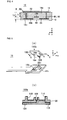
- FIG. 8 is a cross-sectional view of the high-frequency signal line 10 and the battery pack 206 to which the high-frequency signal line 10 is fixed with an installation method according to the first embodiment.
- the ground conductor 22 is electrically connected to the battery pack 206. More specifically, openings Op are provided at the protection layer 14. The ground conductor 22 is partly exposed to the outside via the openings Op provided at the protection layer 14. Solder or a conductive adhesive is charged into the openings Op, so that connection conductors 212 are formed. As a result, the ground conductor 24 is electrically connected to and fixed to the battery pack 206.
- the ground conductors 22 and 24 are maintained at the ground potential not only via the terminal portions 22b and 22c but also via the battery pack 206 that is a metal article. Accordingly, the ground conductors 22 and 24 are more stably maintained at the ground potential.
- the metal article is not limited to a battery pack, and may be a printed circuit board (for example, a ground terminal) or a metal casing.
- FIG. 9 is a cross-sectional view of the high-frequency signal line 10 and the battery pack 206 to which the high-frequency signal line 10 is fixed with an installation method according to the second embodiment.
- the high-frequency signal line 10 is bent along the surface of the battery pack 206 and is attached to the battery pack 206. Since the high-frequency signal line 10 can be easily deformed, it can be bent along the battery pack 206.
- FIG. 10 is an external perspective view of the inside of the electronic apparatus 200 in a case where an installation method according to the third modification is used.
- the high-frequency signal line 10 illustrated in Fig. 6 extends in the x-axis direction on the surface of the battery pack 206 in the negative z-axis direction without being bent.
- connection portions 12b and 12c of the high-frequency signal line 10 illustrated in Fig. 10 are bent with respect to the line portion 12a.
- the high-frequency signal line 10 extends in the x-axis direction on the side surface of the battery pack 206 in the positive y-axis direction. Since the high-frequency signal line 10 can be easily bent, such arrangement can be easily achieved.
- Fig. 11 is an exploded view of a laminate 12 in a high-frequency signal line 10a according to the first modification.
- Fig. 12 is a perspective view of the high-frequency signal line 10a illustrated in Fig. 11 from the z-axis direction.
- Fig. 13 is an equivalent circuit diagram of a part of the high-frequency signal line 10a according to the first modification.
- the difference between the high-frequency signal lines 10 and 10a is the shape of the openings 30.
- the structure of the high-frequency signal line 10a will be described below, focusing on the difference.
- the ground conductor 24 has a ladder shape obtained by alternately disposing a plurality of openings 30 and a plurality of bridge portions 60 along the signal line 20. As illustrated in Fig. 12 , the openings 30 overlap the signal line 20 in plan view from the z-axis direction, and are symmetric with respect to the signal line 20. That is, the signal line 20 traverses the midsections of the openings 30 in the y-axis direction.
- each of the openings 30 is symmetric with respect to a line A that passes through the midsection of the opening 30 in a direction (the x-axis direction) in which the signal line 20 extends and is orthogonal to the signal line 20 (that is, the line A extends in the y-axis direction).
- a line A that passes through the midsection of the opening 30 in a direction (the x-axis direction) in which the signal line 20 extends and is orthogonal to the signal line 20 (that is, the line A extends in the y-axis direction).
- a region including the midsection of the opening 30 in the x-axis direction is defined as a region A1.
- a region corresponding to the bridge portion 60 is defined as a region A2.
- a region between the regions A1 and A2 is defined as a region A3.
- the region A3 is placed on either side of the region A1 in the x-axis direction, and is adjacent to the regions A1 and A2.
- the length of the region A2 in the x-axis direction (that is, the length of the bridge portion 60) is in the range of 25 ⁇ m to 200 ⁇ m. In this embodiment, the length of the region A2 in the x-axis direction is 100 ⁇ m.
- the line A passes through the midsection of the region A1 in the x-axis direction.
- a width W1 of the opening 30 in the region A1 in a direction (the y-axis direction) orthogonal to the signal line 20 is larger than a width W2 of the opening 30 in the region A3 in the y-axis direction. That is, the width of the opening 30 at the midsection thereof in the x-axis direction is larger than that of the other part of the opening 30, and the opening 30 is symmetric with respect to the line A.
- the region A1 is a region in which the opening 30 has the width W1 in the y-axis direction
- the region A3 is a region in which the opening 30 has the width W2 in the y-axis direction. Accordingly, there is a step between the regions A1 and A3 of the opening 30.
- the width W1 is in the range of 500 ⁇ m to 1500 ⁇ m.
- the width W1 is 900 ⁇ m.
- the width W2 is in the range of 250 ⁇ m to 750 ⁇ m.
- the width W2 is 480 ⁇ m.
- a length G1 of the openings 30 in the x-axis direction is in the range of 1 mm to 5 mm.
- the length G1 is 3 mm.
- the length G1 is larger than the width W1 that is the maximum width of the openings 30. It is desired that the length G1 be twice the width W1 or longer.
- no opening is provided between adjacent ones of the openings 30. More specifically, in the region A2 sandwiched between adjacent ones of the openings 30, a conductive layer (the bridge portion 60) uniformly extends and no opening is present.
- the characteristic impedance of the signal line 20 changes in such a manner that, with increasing proximity to the other one of two adjacent bridge portions 60 from one of them, the characteristic impedance increases in the order of a minimum value Z2, an intermediate value Z3, and a maximum value Z1 and then decreases in the order of the maximum value Z1, the intermediate value Z3, and the minimum value Z2.
- the opening 30 has the width W1 in the region A1 and the width W2 smaller than the width W1 in the region A3. Accordingly, the distance between the signal line 20 and the ground conductor 24 in the region A1 is larger than that in the region A3.
- the intensity of a magnetic field generated at the signal line 20 in the region A1 is higher than that of a magnetic field generated at the signal line 20 in the region A3, and an inductance component at the region A1 is increased. That is, in the region A1, an inductive component becomes dominant.
- the bridge portions 60 are provided. Accordingly, the distance between the signal line 20 and the ground conductor 24 in the region A3 is larger than that in the region A2. As a result, a capacitance generated at the signal line 20 in the region A2 is larger than that generated at the signal line 20 in the region A3, and the intensity of a magnetic field generated in the region A2 is lower than that of a magnetic field generated in the region A3. That is, in the region A2, a capacitive component becomes dominant.
- the characteristic impedance of the signal line 20 becomes the maximum value Z1. That is, at a position at which the characteristic impedance of the signal line 20 is the maximum value Z1, the opening 30 has the width W1. In the region A3, the characteristic impedance of the signal line 20 becomes the intermediate value Z3. That is, at a position at which the characteristic impedance of the signal line 20 is the intermediate value Z3, the opening 30 has the width W2. In the region A2, the characteristic impedance of the signal line 20 becomes the minimum value Z2.
- the high-frequency signal line 10 therefore has a circuit configuration illustrated in Fig. 13 . More specifically, in the region A1, since substantially no capacitance is generated between the signal line 20 and the ground conductor 24, the characteristic impedance Z1 is generated mainly by the inductance L1 of the signal line 20. In the region A2, since a large capacitance C3 is generated between the signal line 20 and the ground conductor 24, the characteristic impedance Z2 is generated mainly by the capacitance C3. In the region A3, since a capacitance C2 smaller than the capacitance C3 is generated between the signal line 20 and the ground conductor 24, the characteristic impedance Z3 is generated by an inductance L2 of the signal line 20 and the capacitance C2.
- the characteristic impedance Z3 is, for example, 55 ⁇ .
- the characteristic impedance Z1 is higher than the characteristic impedance Z3, and is, for example, 70 ⁇ .
- the characteristic impedance Z2 is lower than the characteristic impedance Z3, and is, for example, 30 ⁇ .
- the overall characteristic impedance of the high-frequency signal line 10 is 50 ⁇ .
- the characteristic impedance of the signal line 20 changes in such a manner that, with increasing proximity to the other one of two adjacent bridge portions 60 from one of them, the characteristic impedance increases in the order of the minimum value Z2, the intermediate value Z3, and the maximum value Z1 and then decreases in the order of the maximum value Z1, the intermediate value Z3, and the minimum value Z2. Accordingly, the electrode width of the signal line 20 can be increased while reducing the profile of the high-frequency signal line 10a. As a result, the surface area of electrode portions of the signal line 20 and the ground conductors 22 and 24 through which a high-frequency current flows can be increased and the transmission loss of a high-frequency signal is reduced. As illustrated in Fig.
- a length AL corresponding to one cycle (the region A1, the two regions A2, and the regions A3) is a short length that falls within the range of 1 mm to 5 mm, the suppression of unnecessary radiation and the reduction in the transmission loss can be realized even in a higher-frequency range. Since the region A3 is placed on either side of the region A1, a strong magnetic field generated by a current passing through the signal line 20 is not directly transmitted to the region A2. As a result, the ground potential of the region A2 becomes stable and an effect of shielding by the ground conductor 24 is obtained. This leads to the suppression of unnecessary radiation.
- the line width of the signal line 20 can be increased. It is therefore possible to reduce the profile of the high-frequency signal line 10a and realize the reduction in the transmission loss and the suppression of unnecessary radiation while keeping the characteristic impedance of the high-frequency signal line 10a.
- the high-frequency signal line 10a can be therefore easily bent, and can be used after being bent.
- the high-frequency signal line 10a since the ground potential of the ground conductor 24 becomes stable, a transmission loss can be reduced. In addition, a shielding characteristic can be improved. More specifically, in the high-frequency signal line 10a, the width W1 of the opening 30 in the region A1 is larger than the width W2 of the opening 30 in the region A3. Accordingly, in the high-frequency signal line 10a, the magnetic energy of the signal line 20 in the region A1 is larger than that in the region A3. The magnetic energy of the signal line 20 in the region A2 is smaller than that in the region A3.
- the characteristic impedance of the signal line 20 is repeatedly changed in the order of Z2, Z3, Z1, Z3, Z2 ....
- the change in magnetic energy at adjacent portions of the signal line 20 in the x-axis direction is therefore slow.
- the region A3 can suppress the generation of an unnecessary inductance component at the bridge portion 60.
- the mutual inductance component generated between the bridge portion 60 and the signal line 20 can be reduced and the ground potential can be stable.
- the via-hole conductors B1 are disposed in a direction in which the bridge portions 60 extend, the generation of an unnecessary inductance component at the bridge portions 60 can be suppressed.
- the length G1 of the opening 30 in the x-axis direction that is the distance between the bridge portions 60
- the width W1 of the opening 30 in the region A1 the area of the opening 30 can be maximized.
- the occurrence of unnecessary radiation can be suppressed while obtaining a predetermined characteristic impedance.
- the openings 30 are structural units disposed at regular intervals in a direction (the x-axis direction) in which the signal line 20 extends. Accordingly, the frequency characteristic of the characteristic impedance of the signal line 20 in the openings 30 can be determined in accordance with the length of the openings 30 in the x-axis direction. That is, as the length G1 of the openings 30 is reduced, the frequency characteristic of the characteristic impedance of the signal line 20 can be extended to a higher-frequency range. With the increasing length G1 of the openings 30, the width W1 of the openings 30 in the region A1 can be reduced and the openings 30 can extend in a narrow strip form. Since the occurrence of unnecessary radiation can be suppressed and a transmission loss can be reduced, the stable impedance characteristic of the high-frequency signal line 10a in a broader band can be achieved.
- the high-frequency signal line 10a can be used after being bent for the following reason.
- the region A1 since the width of the openings 30 in the y-axis direction is the largest, the high-frequency signal line 10 is most susceptible to bending.
- the region A2 since no opening 30 is provided, it is hardly bent.
- the via-hole conductors B1 and B2, which are less deformable than the dielectric sheets 18, are therefore disposed in the region A2. As a result, the high-frequency signal line 10a can be easily bent in the region A1.
- a predetermined characteristic impedance can also be obtained by adjusting the distance T1 between the signal line 20 and the ground conductor 22 and the distance T2 between the signal line 20 and the ground conductor 24.
- a high-frequency signal transmission mode in the high-frequency signal line 10 is a TEM mode.
- an electric field and a magnetic field are formed in a direction orthogonal to a high-frequency signal transmission direction (the x-axis direction). That is, a magnetic field is generated in the form of circles around the signal line 20, and an electric field radially extends from the signal line 20 to the ground conductors 22 and 24.
- the magnetic field, which forms circles, is only deformed at the openings 30 provided at the ground conductor 22 so that the radii of the circles become larger.
- the magnetic field does not significantly leak from the high-frequency signal line 10a.
- the electric field is partly emitted from the high-frequency signal line 10a. Accordingly, the radiation of an electric field occupies a large part of unnecessary radiation in the high-frequency signal line 10a.
- the increase in the width W1 of the opening 30 in the y-axis direction increases the amount of electric field emitted from the opening 30 (the amount of unnecessary radiation).
- the larger the width W1 the higher the characteristic impedance of the high-frequency signal line 10a.
- the further increase in the width W1 cannot increase the characteristic impedance.
- width W1 reaches approximately half the wavelength of a high-frequency signal, a slot antenna is formed, an electromagnetic wave is emitted, and the amount of unnecessary radiation is increased.
- the longer the length G1 of the opening 30 in the x-axis direction the smaller the area of the signal line 20 facing the ground conductor 22. Accordingly, the line width of the signal line 20 can be increased. As a result, the high-frequency resistance value of the signal line 20 can be reduced.
- the high-frequency resistance value of a counter current (eddy current) in the ground conductor 22 is small.
- the length G1 be larger than the width W1, and, be preferably twice the width W1 or longer.
- the length G1 needs to be much shorter than the wavelength.
- FIG. 14 is an exploded view of the laminate 12 in a high-frequency signal line 10b according to the second modification.
- the difference between the high-frequency signal lines 10b and 10a is the shape of the openings 30. More specifically, as illustrated in Fig. 11 , the width of the openings 30 of the high-frequency signal line 10a in the y-axis direction is discontinuously changed in a stepwise manner. In contrast, the width of the openings 30 of the high-frequency signal line 10b in the y-axis direction is continuously changed. More specifically, the width of the opening 30 in the y-axis direction is continuously reduced as the distance from the center of the opening 30 in the x-axis direction increases. As a result, the magnetic energy and characteristic impedance of the signal line 20 are continuously changed.
- the region A1 has the line A as the center line and includes a part of the opening 30 having the width W1 in the y-axis direction. Accordingly, in the region A1, the characteristic impedance of the signal line 20 becomes the maximum value Z1.
- the region A2 is provided between the openings 30 and includes the bridge portion 60. Accordingly, in the region A2, the characteristic impedance of the signal line 20 becomes the minimum value Z2.
- the region A3 is sandwiched between the regions A1 and A2, and includes a part of the opening 30 having the width W2 in the y-axis direction. Accordingly, in the region A3, the characteristic impedance of the signal line 20 becomes the intermediate value Z3.
- the region A1 needs to include only the part of the opening 30 having the width W1 in the y-axis direction
- the region A3 needs to include only the part of the opening 30 having the width W2 in the y-axis direction. Accordingly, in this embodiment, the boundary between the regions A1 and A3 is not clearly defined.
- the boundary between the regions A1 and A3 is a position at which the width of the opening 30 in the y-axis direction is (W1 + W2)/2.
- the high-frequency signal line 10b having the above-described structure can be used after being bent, can suppress the occurrence of unnecessary radiation, and can reduce a transmission loss in the signal line 20.
- FIG. 15 is an exploded view of the laminate 12 in a high-frequency signal line 10c according to the third modification.
- ground conductors 40 and 42 are disposed on the surface of the dielectric sheet 18b.
- the ground conductor 40 is a rectangular conductor that is present in the positive y-axis direction with respect to the signal line 20 and extends in the x-axis direction.
- the ground conductor 40 is connected to the ground conductors 22 and 24 via the via-hole conductors B1 and B2, respectively.
- the ground conductor 42 is a rectangular conductor that is present in the negative y-axis direction with respect to the signal line 20 and extends in the x-axis direction.
- the ground conductor 42 is connected to the ground conductors 22 and 24 via the via-hole conductors B1 and B2, respectively.
- the ground conductors 40 and 42 are individually disposed on both sides of the signal line 20 in the y-axis direction, the occurrence of unnecessary radiation from the signal line 20 to both sides of the signal line 20 in the y-axis direction is suppressed.
- FIG. 16 is an exploded view of the laminate 12 in a high-frequency signal line 10d according to the fourth modification.
- the difference between the high-frequency signal lines 10d and 10a is the shape of openings (the openings 30 and openings 44a and 44b). More specifically, the openings 44a and 44b are obtained by dividing the opening 30 into two portions in the positive y-axis direction and the negative y-axis direction.
- a linear conductor 46 extending in the x-axis direction is disposed between the openings 44a and 44b.
- the linear conductor 46 is a part of the ground conductor 24 and overlaps the signal line 20 in plan view from the z-axis direction.
- the characteristic impedance of the signal line 20 becomes the maximum value Z1.
- the characteristic impedance of the signal line 20 becomes the intermediate value Z3.
- the characteristic impedance of the signal line 20 becomes the minimum value Z2.
- the line width of the linear conductor 46 is smaller than that of the signal line 20. Accordingly, the signal line 20 protrudes from the linear conductor 46 in plan view from the z-axis direction.
- the line width of the linear conductor 46 may be larger than that of the signal line 20, and the signal line 20 does not necessarily have to protrude from the linear conductor 46. That is, the openings 44a and 44b do not necessarily have to overlap the signal line 20. Similarly, the openings 30 do not necessarily have to overlap the signal line 20.
- the high-frequency signal line 10d In the high-frequency signal line 10d, the direction of high-frequency currents flowing through the linear conductor 46 and the ground conductors 22 and 24 is opposite to that of a high-frequency current flowing through the signal line 20. Accordingly, even in a case where the signal line 20 protrudes from the linear conductor 46, the high-frequency signal line 10d can more effectively suppress the occurrence of unnecessary radiation as compared with the high-frequency signal line 10.
- FIG. 17 is an exploded view of the laminate 12 in a high-frequency signal line 10e according to the fifth modification.
- Fig. 18 is a perspective view of the high-frequency signal line 10e illustrated in Fig. 17 from the z-axis direction.
- a first difference between the high-frequency signal lines 10e and 10a is that the line width of the signal line 20 at the bridge portions 60 is smaller than that of the signal line 20 at positions at which the characteristic impedance of the signal line 20 becomes the maximum value Z1.
- a second difference between the high-frequency signal lines 10e and 10a is that the opening 30 tapers between a position at which the characteristic impedance of the signal line 20 becomes the intermediate value Z3 (that is, the position at which the width W2 of the opening 30 in the y-axis direction is obtained) and a position at which the characteristic impedance of the signal line 20 becomes the maximum value Z1 (that is, the position at which the width W1 of the opening 30 in the y-axis direction is obtained).
- a third difference between the high-frequency signal lines 10e and 10a is that the opening 30 tapers between a position at which the characteristic impedance of the signal line 20 becomes the intermediate value Z3 (that is, the position at which the width W2 of the opening 30 in the y-axis direction is obtained) and the bridge portion 60.
- the region A1 is a region in which the width W1 of the opening 30 in the y-axis direction is obtained.
- the region A2 is a region corresponding to the bridge portion 60.
- the region A3 is sandwiched between the regions A1 and A2, and includes a part of the opening 30 having the width W2 in the y-axis direction.
- the signal line 20 has a line width Wb in the region A2.
- the signal line 20 has a line width Wa larger than the line width Wb in the region A1.
- the line width Wa is in the range of 100 ⁇ m to 500 ⁇ m.
- the line width Wa is 350 ⁇ m.
- the line width Wb is in the range of 25 ⁇ m to 250 ⁇ m.
- the line width Wb is 100 ⁇ m. Since the line width of the signal line 20 in the region A2 is smaller than that in the region A1, the area of a part of the signal line 20 overlapping the bridge portion 60 is reduced.
- a stray capacitance generated between the signal line 20 and the bridge portion 60 is reduced. Furthermore, since a part of the signal line 20 overlapping the opening 30 has the line width Wa, the increase in the inductance value of the part of the signal line 20 can be suppressed. Still furthermore, since the line width of the signal line 20 is not wholly narrowed but partly narrowed, the increase in the resistance value of the signal line 20 is suppressed.
- the signal line 20 tapers with the change in the line width thereof. As a result, at a part of the signal line 20 whose line width varies, the change in a resistance value becomes slow and the occurrence of the reflection of a high-frequency signal is suppressed.
- the opening 30 tapers between the position at which the width W2 of the opening 30 in the y-axis direction is obtained and the position at which the width W1 of the opening 30 in the y-axis direction is obtained. That is, the end portion of the region A3 in the x-axis direction tapers. As a result, the loss of a current passing through the ground conductor 24 is reduced.
- the opening 30 tapers between the position at which the width W2 of the opening 30 in the y-axis direction is obtained and the bridge portion 60. That is, both end portions of the bridge portion 60 in the y-axis direction taper. A part of the bridge portion 60 overlapping the signal line 20 therefore has a line width smaller than that of the other part of the bridge portion 60 in the x-axis direction. As a result, a stray capacitance generated between the bridge portion 60 and the signal line 20 is reduced. Since the line width of the bridge portion 60 is not wholly narrowed but partly narrowed, the increases in the resistance value and inductance value of the bridge portion 60 are suppressed.
- FIG. 19 is an exploded view of the laminate 12 in a high-frequency signal line 10f according to the sixth modification.
- Fig. 20 is a perspective view of the high-frequency signal line 10f illustrated in Fig. 19 from the z-axis direction.
- the difference between the high-frequency signal lines 10f and 10a is that a floating conductor 50 is disposed. More specifically, the high-frequency signal line 10f further includes a dielectric sheet 18d and the floating conductor 50.
- the dielectric sheet 18d is formed on the surface of the dielectric sheet 18c in the negative z-axis direction.
- the floating conductor 50 is a rectangular conductive layer and is disposed on the surface of the dielectric sheet 18d.
- the floating conductor 50 is located on the opposite side of the ground conductor 24 respect to the signal line 20.
- the floating conductor 50 faces the signal line 20 and the ground conductor 24 in plan view from the z-axis direction.
- a width W3 of the floating conductor 50 in the y-axis direction is smaller than the width W1 of the opening 30 in the region A1 and is larger than the width W2 of the opening 30 in the region A3.
- the bridge portions 60 are covered with the floating conductor 50.
- the floating conductor 50 is not electrically connected to conductive layers such as the signal line 20 and the ground conductor 24, and provides a floating potential.
- the floating potential is a potential between the signal line 20 and the ground conductor 24.
- the characteristic impedance of the signal line 20 is hardly changed. More specifically, since the floating conductor 50 is not electrically connected to the signal line 20 and the ground conductors 22 and 24, the floating conductor 50 provides a floating potential. Accordingly, the stray capacitance between the signal line 20 and the floating conductor 50 and the stray capacitance between the floating conductor 50 and the ground conductor 24 are serial connected to each other.
- the width W3 of the floating conductor 50 is smaller than the width W1 of the opening 30 in the region A1 and is larger than the width W2 of the opening 30 in the region A3. Accordingly, the area of a part of the floating conductor 50 facing the ground conductor 24 is small, and the stray capacitance between the ground conductor 24 and the floating conductor 50 is also small. A capacitance obtained by combining the stray capacitance between the signal line 20 and the floating conductor 50 and the stray capacitance between the floating conductor 50 and the ground conductor 24, which are serial connected to each other, is therefore small. With the floating conductor 50, the amount of change in the characteristic impedance of the signal line 20 becomes small.
- Fig. 21 is an external perspective view of a high-frequency signal line 10g according to the second embodiment of the present invention.
- Fig. 22 is an exploded view of the dielectric body 12 in the high-frequency signal line 10g illustrated in Fig. 21 .
- Fig. 23 is a cross-sectional view of the high-frequency signal line 10g illustrated in Fig. 21 .
- Fig. 24 is a cross-sectional view of the high-frequency signal line 10g. Referring to Figs.
- a lamination direction in the high-frequency signal line 10g is defined as a z-axis direction
- a longitudinal direction in the high-frequency signal line 10g is defined as an x-axis direction
- a direction orthogonal to the x-axis direction and the z-axis direction is defined as a y-axis direction.
- the high-frequency signal line 10g is used to connect two high-frequency circuits in an electronic apparatus such as a mobile telephone.
- the high-frequency signal line 10g includes the dielectric body 12, the external terminal 16 (16a and 16b), the signal line 20, the ground conductors 22 and 24, an adhesive layer 70, a cover sheet 72, the via-hole conductors b1, b2, B1, and B2, and the connectors 100a and 100b.
- the dielectric body 12 extends in the x-axis direction in plan view from the z-axis direction, and includes the line portion 12a and the connection portions 12b and 12c.
- the dielectric body 12 is a laminate obtained by laminating the protection layer 14 and the dielectric sheet (insulating layer) 18 (18a to 18c), which are illustrated in Fig. 22 , in this order from the positive z-axis direction to the negative z-axis direction.
- the dielectric body 12 has flexibility, and has two main surfaces.
- the main surface of the dielectric body 12 in the positive z-axis direction is referred to as a surface (the first main surface) and the main surface of the dielectric body 12 in the negative z-axis direction is referred to as an undersurface (the second main surface) .
- the line portion 12a extends in the x-axis direction.
- the connection portion 12b is connected to the end of the line portion 12a in the negative x-axis direction
- the connection portion 12c is connected to the end of the line portion 12a in the positive x-axis direction.
- the connection portions 12b and 12c are rectangular in shape.
- the width of the connection portions 12b and 12c in the y-axis direction is larger than that of the line portion 12a in the y-axis direction.
- the dielectric sheet 18 extends in the x-axis direction in plan view from the z-axis direction, and is an insulating layer having the same shape as the dielectric body 12.
- the dielectric sheet 18 is made of a thermoplastic resin such as polyimide or liquid crystal polymer having flexibility.
- the thickness T1 of the dielectric sheet 18a is larger than the thickness T2 of the dielectric sheet 18b.
- the thickness T1 is in the range of 50 ⁇ m to 300 ⁇ m. In this embodiment, the thickness T1 is 150 ⁇ m.
- the thickness T2 is in the range of 10 ⁇ m to 100 ⁇ m. In this embodiment, the thickness T2 is 50 ⁇ m.
- the main surface of the dielectric sheet 18 in the positive z-axis direction is referred to as a surface
- the main surface of the dielectric sheet 18 in the negative z-axis direction is referred to as an undersurface.
- the dielectric sheet 18a includes the line portion 18a-a and the connection portions 18a-b and 18a-c.
- the dielectric sheet 18b includes the line portion 18b-a and the connection portions 18b-b and 18b-c.
- the dielectric sheet 18c includes the line portion 18c-a and the connection portions 18c-b and 18c-c.
- the line portions 18a-a, 18b-a, and 18c-a form the line portion 12a.
- the connection portions 18a-b, 18b-b, and 18c-b form the connection portion 12b.
- the connection portions 18a-c, 18b-c, and 18c-c form the connection portion 12c.
- the external terminal 16a is a rectangular conductor disposed near the center of the surface of the connection portion 18a-b.
- the external terminal 16b is a rectangular conductor disposed near the center of the surface of the connection portion 18a-c.
- the external terminals 16a and 16b are made of a metal material such as silver or copper having low resistivity.
- the surfaces of the external terminals 16a and 16b are gold-plated.
- the signal line 20 is a linear conductor disposed in the dielectric body 12, and extends in the x-axis direction on the surface of the dielectric sheet 18b. Both ends of the signal line 20 individually overlap the external terminals 16a and 16b in plan view from the z-axis direction.
- the line width of the signal line 20 is in the range of 100 ⁇ m to 500 ⁇ m. In this embodiment, the line width of the signal line 20 is 240 ⁇ m.
- the signal line 20 is made of a metal material such as silver or copper having low resistivity.
- the ground conductor 22 (first ground conductor) is disposed between the signal line 20 and the first main surface (that is, in the positive z-axis direction with respect to the signal line 20), and, more specifically, is disposed on the surface of the dielectric sheet 18a nearest to the surface of the dielectric body 12.
- the ground conductor 22 extends in the x-axis direction on the surface of the dielectric sheet 18a, and faces the signal line 20 via the dielectric sheet 18a. No opening is disposed at a part of the ground conductor 22 facing the signal line 20. That is, the ground conductor 22 is a solid electrode that continuously extends in the x-axis direction along the signal line 20 in the line portion 12a.
- the ground conductor 22 does not necessarily have to completely cover the line portion 12a.
- a small hole may be provided at a predetermined position on the ground conductor 22.
- the ground conductor 22 is made of a metal material such as silver or copper having low resistivity.
- the ground conductor 22 includes the line portion 22a and the terminal portions 22b and 22c.
- the line portion 22a is disposed on the surface of the line portion 18a-a, and extends in the x-axis direction.
- the terminal portion 22b is disposed on the surface of the line portion 18a-b, and is a rectangular ring surrounding the external terminal 16a.
- the terminal portion 22b is connected to the end of the line portion 22a in the negative x-axis direction.
- the terminal portion 22c is disposed on the surface of the line portion 18a-c, and is a rectangular ring surrounding the external terminal 16b.
- the terminal portion 22c is connected to the end of the line portion 22a in the positive x-axis direction.
- the ground conductor 24 (second ground conductor) is disposed between the signal line 20 and the second main surface (that is, in the negative z-axis direction with respect to the signal line 20), and, more specifically, is disposed on the surface of the dielectric sheet 18c.
- the ground conductor 24 is therefore disposed between the dielectric sheets 18b and 18c.
- the ground conductor 24 extends in the x-axis direction on the surface of the dielectric sheet 18c, and faces the signal line 20 via the dielectric sheet 18b. That is, the ground conductor 24 faces the ground conductor 22 via the signal line 20 sandwiched therebetween.
- the ground conductor 24 is made of a metal material such as silver or copper having low resistivity.
- the ground conductor 24 includes the line portion 24a and the terminal portions 24b and 24c.
- the line portion 24a is disposed on the surface of the line portion 18c-a, and extends in the x-axis direction.
- the line portion 24a has a ladder shape obtained by alternately disposing a plurality of openings 30 at which no conductive layer is formed and a plurality of bridge portions 60 at which a conductive layer is formed along the signal line 20.
- the openings 30 are rectangular in shape and overlap the signal line 20 in plan view from the z-axis direction. Accordingly, the signal line 20 alternately overlaps the openings 30 and the bridge portions 60 in plan view from the z-axis direction.
- the openings 30 are arranged at regular intervals.
- the terminal portion 24b is disposed on the surface of the line portion 18c-b, and is a rectangular ring.
- the terminal portion 24b is connected to the end of the line portion 24a in the negative x-axis direction.
- the terminal portion 24c is disposed on the surface of the line portion 18c-c, and is a rectangular ring.
- the terminal portion 24c is connected to the end of the line portion 24a in the positive x-axis direction.
- the signal line 20 is sandwiched between the ground conductors 22 and 24 via the dielectric layers 18a and 18b. That is, the signal line 20 and the ground conductors 22 and 24 form a triplate strip line structure.
- the distance between the signal line 20 and the ground conductor 22 is substantially equal to the thickness T1 of the dielectric sheet 18a, and, for example, is in the range of 50 ⁇ m to 300 ⁇ m. In this embodiment, the distance between the signal line 20 and the ground conductor 22 is 150 ⁇ m.
- Fig. 24 the distance between the signal line 20 and the ground conductor 22 is substantially equal to the thickness T1 of the dielectric sheet 18a, and, for example, is in the range of 50 ⁇ m to 300 ⁇ m. In this embodiment, the distance between the signal line 20 and the ground conductor 22 is 150 ⁇ m.
- the distance between the signal line 20 and the ground conductor 24 is substantially equal to the thickness T2 of the dielectric sheet 18b, and, for example, is in the range of 10 ⁇ m to 100 ⁇ m. In this embodiment, the distance between the signal line 20 and the ground conductor 24 is 50 ⁇ m. That is, design is performed so that the thickness T1 is larger than the thickness T2.
- the via-hole conductor b1 passes through the connection portion 18a-b of the dielectric sheet 18a in the z-axis direction, and connects the external terminal 16a and the end of the signal line 20 in the negative x-axis direction.
- the via-hole conductor b2 passes through the connection portion 18a-c of the dielectric sheet 18a in the z-axis direction, and connects the external terminal 16b and the end of the signal line 20 in the positive x-axis direction. As a result, the signal line 20 is connected between the external terminals 16a and 16b.
- the via-hole conductors b1 and b2 are made of a metal material such as silver or copper having low resistivity.
- the via-hole conductors B1 pass through the line portion 18a-a of the dielectric sheet 18a in the z-axis direction, and are disposed at the line portion 18a-a.
- the via-hole conductors B2 pass through the line portion 18b-a of the dielectric sheet 18b in the z-axis direction, and are disposed at the line portion 18b-a.
- the via-hole conductor B1 and the via-hole conductor B2 are connected to each other, so that a single via-hole conductor is formed and connects the ground conductors 22 and 24.
- the via-hole conductors B1 and B2 are made of a metal material such as silver or copper having low resistivity.
- the protection layer 14 covers the substantially entire surface of the dielectric sheet 18a. As a result, the protection layer 14 covers the ground conductor 22.
- the protection layer 14 is made of a flexible resin such as a resist material.
- the protection layer 14 includes the line portion 14a and the connection portions 14b and 14c.
- the line portion 14a covers the entire surface of the line portion 18a-a, thereby covering the line portion 22a.
- connection portion 14b is connected to the end of the line portion 14a in the negative x-axis direction, and covers the surface of the connection portion 18a-b.
- the openings Ha to Hd are formed.
- the opening Ha is a rectangular opening formed at the center of the connection portion 14b.
- the external terminal 16a is exposed to the outside via the opening Ha.
- the opening Hb is a rectangular opening formed in the positive y-axis direction with respect to the opening Ha.
- the opening Hc is a rectangular opening formed in the negative x-axis direction with respect to the opening Ha.
- the opening Hd is a rectangular opening formed in the negative y-axis direction with respect to the opening Ha.
- the terminal portion 22b is exposed to the outside via the openings Hb to Hd, thereby functioning as an external terminal.
- connection portion 14c is connected to the end of the line portion 14a in the positive x-axis direction, and covers the surface of the connection portion 18a-c.
- the openings He to Hh are formed.
- the opening He is a rectangular opening formed at the center of the connection portion 14c.
- the external terminal 16b is exposed to the outside via the opening He.
- the opening Hf is a rectangular opening formed in the positive y-axis direction with respect to the opening He.
- the opening Hg is a rectangular opening formed in the positive x-axis direction with respect to the opening He.
- the opening Hh is a rectangular opening formed in the negative y-axis direction with respect to the opening He.
- the terminal portion 22c is exposed to the outside via the openings Hf to Hh, thereby functioning as an external terminal.
- the adhesive layer 70 is made of an insulating adhesive, and is formed on the first main surface of the dielectric body 12. More specifically, the adhesive layer 70 is formed so that it extends in the x-axis direction on the line portion 14a of the protection layer 14 in the dielectric body 12.
- the cover sheet 72 is a flexible sheet that is releasably attached to the adhesive layer 70.
- the adhesive layer 70 and the cover sheet 72 form an adhesive tape with a cover sheet thereon.
- the connectors 100a and 100b are disposed on the surfaces of the connection portions 12b and 12c, respectively.
- the descriptions of the structures of the connectors 100a and 100b have been made, and will be therefore omitted.
- Fig. 25 is a cross-sectional view of the electronic apparatus 200.
- the electronic apparatus 200 includes the high-frequency signal line 10g, the circuit boards 202a and 202b, the receptacles 204a and 204b, the battery pack (article) 206, and the casing 210.
- a transmission circuit or a receiving circuit including an antenna is disposed at the circuit board 202a.
- a feeding circuit is disposed at the circuit board 202b.
- the battery pack 206 is, for example, a lithium-ion secondary battery, and the surface of the battery pack 206 is covered with an insulator.
- the circuit board 202a, the battery pack 206, and the circuit board 202b are arranged in this order from the negative x-axis direction to the positive x-axis direction.
- the receptacles 204a and 204b are disposed on the main surfaces of the circuit boards 202a and 202b in the negative z-axis direction, respectively.
- the connectors 100a and 100b are connected to the receptacles 204a and 204b, respectively.
- a high-frequency signal having the frequency of, for example, 2 GHz transmitted between the circuit boards 202a and 202b is applied to the center conductors 108 of the connectors 100a and 100b via the receptacles 204a and 204b.
- the external conductors 110 of the connectors 100a and 100b are held at the ground potential via the circuit boards 202a and 202b and the receptacles 204a and 204b, respectively.
- the high-frequency signal line 10g electrically and physically connects the circuit boards 202a and 202b.
- the high-frequency signal line 10g is fixed to the battery pack 206 via the adhesive layer 70 from which the cover sheet 72 has been detached.
- the surface of the dielectric body 12 is a main surface located on the side of the ground conductor 22 with respect to the signal line 20. Accordingly, between the signal line 20 and the battery pack 206, there is the ground conductor 22 that is a solid conductor (that continuously extends in the x-axis direction).
- the high-frequency signal line 10g is bonded to the battery pack 206, but may be bonded to a printed circuit board or the casing of an electronic apparatus.
- the surface of the battery pack 206 is covered with an insulator, but may be covered with a conductor such as metal.
- Fig. 26 is a cross-sectional view of the high-frequency signal line 10g and the battery pack 206 to which the high-frequency signal line 10g is bonded.
- the cover sheet 72 is partly detached from the adhesive layer 70.
- the exposed part of the adhesive layer 70 is bonded to the battery pack 206.
- the adhesive layer 70 is bonded to the battery pack 206 while detaching the cover sheet 72 from the adhesive layer 70.
- the high-frequency signal line 10g is bonded to the battery pack 206 using a procedure similar to a procedure for the placement of a sticky label. Referring to Fig. 26 , the structures of the ground conductors 22 and 24 and the signal line 20 are partly illustrated.
- the high-frequency signal line 10g having the above-described structure can be fixed to an article in narrow space. More specifically, components such as a fixing bracket and a screw for fixing the high-frequency signal line 10g to an article becomes unnecessary. As a result, the high-frequency signal line 10g can be fixed to an article in narrow space in an electronic apparatus. Furthermore, since a screw for fixing the high-frequency signal line 10g to an article is not used, no screw hole is formed at the battery pack 206.
- the adhesive layer 70 is bonded to the battery pack 206 while detaching the cover sheet 72 from the adhesive layer 70.
- the high-frequency signal line 10g is bonded to the battery pack 206 using a procedure similar to a procedure for the placement of a sticky label. Accordingly, in the high-frequency signal line 10g, it is unnecessary to perform screwing with a fixed structure for the coaxial cable disclosed in Patent Literature 1.
- the high-frequency signal line 10g can be easily fixed to the battery pack 206.
- the high-frequency signal line 10g does not need components such as a fixing bracket and a screw, no stray capacitance is generated between the signal line 20 and each of the fixing bracket and the screw. Accordingly, the deviation of the characteristic impedance of the high-frequency signal line 10g from a predetermined characteristic impedance is suppressed.
- Fig. 27 is an exploded view of the laminate 12 in a high-frequency signal line 10h according to the first modification.
- the high-frequency signal line 10a may include the adhesive layer 70 and the cover sheet 72.
- Fig. 28 is an exploded view of the laminate 12 in a high-frequency signal line 10i according to the second modification.
- the high-frequency signal line 10b may include the adhesive layer 70 and the cover sheet 72.
- FIG. 29 is an exploded view of the laminate 12 in a high-frequency signal line 10j according to the third modification.
- the high-frequency signal line 10c may include the adhesive layer 70 and the cover sheet 72.
- FIG. 30 is an exploded view of the laminate 12 in a high-frequency signal line 10k according to the fourth modification.
- the high-frequency signal line 10d may include the adhesive layer 70 and the cover sheet 72.
- FIG. 31 is an exploded view of the laminate 12 in a high-frequency signal line 101 according to the fifth modification.
- the high-frequency signal line 10e may include the adhesive layer 70 and the cover sheet 72.
- FIG. 32 is an exploded view of the laminate 12 in a high-frequency signal line 10m according to the sixth modification.
- the high-frequency signal line 10f may include the adhesive layer 70 and the cover sheet 72.
- Fig. 33 is an external perspective view of a high-frequency signal line 10n according to the seventh modification.
- Fig. 34 is an exploded view of the dielectric body 12 in the high-frequency signal line 10n illustrated in Fig. 33 .
- Fig. 35 is a cross-sectional view of the high-frequency signal line 10n illustrated in Fig. 33 .
- the difference between the high-frequency signal lines 10n and 10g is that the adhesive layer 70 is partly absent and a pad 74 is disposed. More specifically, as illustrated in Figs. 33 and 34 , the line portion 14a of the protection layer 14 and the adhesive layer 70 are partly absent.
- the pad 74 made of solder is formed at a position at which the line portion 14a of the protection layer 14 and the adhesive layer 70 are absent.
- the pad 74 is formed on the ground conductor 22, and is connected to the ground conductor 22.
- the high-frequency signal line 10n having the above-described structure is fixed to the battery pack 206 covered with a metal cover via the adhesive layer 70.
- the pad 74 is in contact with the metal cover of the battery pack 206.
- the ground conductor 22 is electrically connected to the metal cover of the battery pack 206 via the pad 74.
- the ground conductor 22 is held at the ground potential not only via the connectors 100a and 100b but also via the metal cover. That is, the potential of the ground conductor 22 is more stably brought close to the ground potential.
- the pad 74 may be in contact with the metal casing of an electronic apparatus or the land of a printed circuit board.
- FIG. 36 is an external perspective view of a high-frequency signal line 10o according to the eighth modification.
- Fig. 37 is an exploded view of the dielectric body 12 in the high-frequency signal line 10o illustrated in Fig. 36 .
- Fig. 38 is a cross-sectional view of the high-frequency signal line 10o illustrated in Fig. 36 .
- the difference between the high-frequency signal lines 10o and 10g is that the adhesive layer 70 is a conductive adhesive. More specifically, as illustrated in Figs. 36 and 37 , a part of the line portion 14a of the protection layer 14 is absent. The ground conductor 22 is therefore disposed on the first main surface of the dielectric body 12. At a position at which the line portion 14a is absent, the adhesive layer 70 and the cover sheet 72 are formed. As a result, the adhesive layer 70 is formed on the ground conductor 22, and is connected to the ground conductor 22.
- the high-frequency signal line 10o having the above-described structure is fixed to the battery pack 206 covered with a metal cover (conductive portion) via the adhesive layer 70.
- the adhesive layer 70 is in contact with the metal cover of the battery pack 206.
- the ground conductor 22 is electrically connected to the metal cover of the battery pack 206 via the adhesive layer 70.
- the ground conductor 22 is held at the ground potential not only via the connectors 100a and 100b but also via the metal cover. That is, the potential of the ground conductor 22 is more stably brought close to the ground potential.
- FIG. 39 is an external perspective view of a high-frequency signal line 10p according to the ninth modification.
- Fig. 40 is an exploded view of the dielectric body 12 in the high-frequency signal line 10p illustrated in Fig. 39 .
- Fig. 41 is a cross-sectional view of the high-frequency signal line 10p illustrated in Fig. 39 .
- the difference between the high-frequency signal lines 10p and 10o is that each of the adhesive layer 70 and the cover sheet 72 is divided into two portions.
- the high-frequency signal line 10p having the above-described structure is fixed to a printed circuit board 306 with a land (conductive portion) 307 thereon via the adhesive layer 70.
- the land 307 is obtained by applying a coating 309 to a base electrode 308 made of, for example, Cu.
- the adhesive layer 70 is in contact with the land 307.
- the ground conductor 22 is electrically connected to the land 307 via the adhesive layer 70.
- the ground conductor 22 is held at the ground potential not only via the connectors 100a and 100b but also via the land 307. That is, the potential of the ground conductor 22 is more stably brought close to the ground potential.
- the two adhesive layers are preferably in contact with an article such as a land so that they are held at a ground potential. Only one of the two adhesive layers may be held at the ground potential, or none of them may be connected to the ground.
- Fig. 42 is an exploded view of the dielectric body 12 in a high-frequency signal line 10q according to the tenth modification.
- the difference between the high-frequency signal lines 10q and 10o is that the ground conductor 24 is disposed on the undersurface of the dielectric sheet 18b. More specifically, the signal line 20 is disposed on the surface of the dielectric sheet 18b, and the ground conductor 24 is disposed on the undersurface of the dielectric sheet 18b. In the high-frequency signal line 10q, the dielectric sheet 18c is not formed and a protection layer 15 is formed.
- the high-frequency signal line 10q having the above-described structure uses only two dielectric sheets 18, the high-frequency signal line 10q can be easily created.
- a high-frequency signal line according to the present invention is not limited to the high-frequency signal lines 10 and 10a to 10q according to an embodiment of the present invention, and various changes can be made to these high-frequency signal lines without departing from the scope of the present invention.
- a plurality of openings 30 have the same shape, but may have different shapes.
- the length of a predetermined one of the openings 30 in the x-axis direction may be longer than that of the other ones of the openings 30 in the x-axis direction.
- the structures of the high-frequency signal lines 10 and 10a to 10q may be combined.
- the characteristic impedance of the signal line 20 changes in such a manner that, with increasing proximity to the other one of two adjacent bridge portions 60 from one of them, the characteristic impedance increases in the order of the minimum value Z2, the intermediate value Z3, and the maximum value Z1 and then decreases in the order of the maximum value Z1, the intermediate value Z3, and the minimum value Z2.
- the characteristic impedance of the signal line 20 may change in such a manner that, with increasing proximity to the other one of two adjacent bridge portions 60 from one of them, the characteristic impedance increases in the order of the minimum value Z2, the intermediate value Z3, and the maximum value Z1 and then decreases in the order of the maximum value Z1, an intermediate value Z4, and the minimum value Z2.
- each of the openings 30, 31, 44a, and 44 may not be symmetric with respect to the line A.
- the intermediate value Z4 needs to be larger than the minimum value Z2 and smaller than the maximum value Z1.
- the minimum values Z2 do not necessarily have to be the same.
- the minimum value Z2 obtained in one of the bridge portions 60 needs to be smaller than the intermediate value Z3
- the minimum value Z2 obtained in the other one of the bridge portions 60 needs to be smaller than the intermediate value Z4.
- the adhesive layer 70 and the cover sheet 72 may further formed on the second main surface of the dielectric body 12.
- the present invention is useful for a high-frequency signal line and an electronic apparatus, and, in particular, has an advantage in its suitability for fixing a high-frequency signal line to an article in narrow space.
Abstract
Description
- The present invention relates to high-frequency signal lines and electronic apparatuses, and, more particularly, to a high-frequency signal line including a signal line and ground conductors facing the signal line and an electronic apparatus.
- As a high-frequency line for connecting high-frequency circuits, a coaxial cable is generally used. Since coaxial cables are easily deformed (bent) and are inexpensive, they are widely used.
- In recent years, high-frequency apparatuses such as mobile communication terminals have been miniaturized. Accordingly, in such a high-frequency apparatus, it is difficult to obtain space for a coaxial cable having a circular cross section. A high-frequency signal line obtained by forming a strip line in a flexible laminate is therefore sometimes used.
- Triplate strip lines have a structure in which a signal line is sandwiched between ground conductors. Since the thickness of such a high-frequency signal line in a lamination direction is smaller than the diameters of coaxial cables, the high-frequency signal line can fit into small space into which the coaxial cables cannot fit.
- As the invention related to the high-frequency signal line, a flexible substrate disclosed in
Patent Literature 1 is known. In the flexible substrate disclosed inPatent Literature 1, since a ground conductor has an opening portion, a strip line can be more easily bent as compared with a strip line sandwiched between ground conductors formed on the entire surfaces. - However, in the flexible substrate disclosed in
Patent Literature 1, an electromagnetic field may exit from the opening portion to the outside of the flexible substrate. In a case where an article such as a dielectric or a metal body is disposed around the flexible substrate, electromagnetic field coupling occurs between the signal line in the flexible substrate and the article. As a result, the characteristic impedance of the signal line in the flexible substrate may deviate from a predetermined characteristic impedance. -
- PTL 1: Japanese Unexamined Patent Application Publication No.
2007-123740 - It is an object of the present invention to provide a high-frequency signal line that can be easily bent and can suppress the deviation of the characteristic impedance of a signal line included therein from a predetermined characteristic impedance and an electronic apparatus. Solution to Problem
- A high-frequency signal line according to an embodiment of the present invention includes a laminate that is obtained by laminating insulating layers and has a first main surface and a second main surface, a linear signal line disposed in the laminate, a first ground conductor that is disposed in the laminate, faces the signal line via one of the insulating layers, and continuously extends along the signal line, and a second ground conductor that is disposed in the laminate, faces the first ground conductor via the signal line sandwiched therebetween, and has a plurality of openings arranged along the signal line. The first main surface placed on a side of the first ground conductor with respect to the signal line is a surface to be in contact with an article.
- A high-frequency signal line according to another embodiment of the present invention includes an element assembly having a first main surface and a second main surface, a linear signal line disposed in the element assembly, a first ground conductor that is disposed on a side of the first main surface with respect to the signal line in the element assembly and faces the signal line, and a second ground conductor that faces the first ground conductor via the signal line sandwiched therebetween in the element assembly, and has an opening arranged along the signal line, an adhesive layer formed on the first main surface, and a cover layer releasably attached to the adhesive layer.
- An electronic apparatus according to an embodiment of the present invention includes the high-frequency signal line and an article. The high-frequency signal line is fixed to the article via the adhesive layer from which the cover layer has been detached.
- According to the present invention, a signal line can be easily bent, and the deviation of the characteristic impedance of the signal line from a predetermined characteristic impedance can be suppressed.
-
- [
Fig. 1] Fig. 1 is an external perspective view of a high-frequency signal line according to a first embodiment of the present invention. - [
Fig. 2] Fig. 2 is an exploded view of a dielectric body in the high-frequency signal line illustrated inFig. 1 . - [
Fig. 3] Fig. 3 is a cross-sectional view of the high-frequency signal line illustrated inFig. 1 . - [
Fig. 4] Fig. 4 is a cross-sectional view of a high-frequency signal line. - [
Fig. 5] Fig. 5 includes an external perspective view and a cross-sectional view of a connector in a high-frequency signal line. - [
Fig. 6] Fig. 6 includes plan views of an electronic apparatus including a high-frequency signal line from a y-axis direction and a z-axis direction. - [
Fig. 7] Fig. 7 is a cross-sectional view of a portion C illustrated inFig. 6(a) . - [
Fig. 8] Fig. 8 is a cross-sectional view of a high-frequency signal line and a battery pack to which the high-frequency signal line is fixed with an installation method according to a first modification of the first embodiment. - [
Fig. 9] Fig. 9 is a cross-sectional view of a high-frequency signal line and a battery pack to which the high-frequency signal line is fixed with an installation method according to a second modification of the first embodiment. - [
Fig. 10] Fig. 10 is an external perspective view of the inside of an electronic apparatus in a case where an installation method according to a third modification of the first embodiment is used. - [
Fig. 11] Fig. 11 is an exploded view of a laminate in a high-frequency signal line according to the first modification of the first embodiment. - [
Fig. 12] Fig. 12 is a perspective view of the high-frequency signal line illustrated inFig. 11 from the z-axis direction. - [
Fig. 13] Fig. 13 is an equivalent circuit diagram of a part of a high-frequency signal line according to the first modification of the first embodiment. - [
Fig. 14] Fig. 14 is an exploded view of a laminate in a high-frequency signal line according to the second modification of the first embodiment. - [
Fig. 15] Fig. 15 is an exploded view of a laminate in a high-frequency signal line according to the third modification of the first embodiment. - [
Fig. 16] Fig. 16 is an exploded view of a laminate in a high-frequency signal line according to a fourth modification of the first embodiment. - [
Fig. 17] Fig. 17 is an exploded view of a laminate in a high-frequency signal line according to a fifth modification of the first embodiment. - [
Fig. 18] Fig. 18 is a perspective view of the high-frequency signal line illustrated inFig. 17 from the z-axis direction. - [
Fig. 19] Fig. 19 is an exploded view of a laminate in a high-frequency signal line according to a sixth modification of the first embodiment. - [
Fig. 20] Fig. 20 is a perspective view of the high-frequency signal line illustrated inFig. 19 from the z-axis direction. - [
Fig. 21] Fig. 21 is an external perspective view of a high-frequency signal line according to a second embodiment of the present invention. - [
Fig. 22] Fig. 22 is an exploded view of a dielectric body in the high-frequency signal line illustrated inFig. 21 . - [
Fig. 23] Fig. 23 is a cross-sectional view of the high-frequency signal line illustrated inFig. 21 . - [
Fig. 24] Fig. 24 is a cross-sectional view of a high-frequency signal line. - [
Fig. 25] Fig. 25 is a cross-sectional view of anelectronic apparatus 200. - [
Fig. 26] Fig. 26 is a cross-sectional view of a high-frequency signal line and a battery pack to which the high-frequency signal line is bonded. - [
Fig. 27] Fig. 27 is an exploded view of a laminate in a high-frequency signal line according to a first modification of the second embodiment. - [
Fig. 28] Fig. 28 is an exploded view of a laminate in a high-frequency signal line according to a second modification of the second embodiment. - [
Fig. 29] Fig. 29 is an exploded view of a laminate in a high-frequency signal line according to a third modification of the second embodiment. - [
Fig. 30] Fig. 30 is an exploded view of a laminate in a high-frequency signal line according to a fourth modification of the second embodiment. - [
Fig. 31] Fig. 31 is an exploded view of a laminate in a high-frequency signal line according to a fifth modification of the second embodiment. - [
Fig. 32] Fig. 32 is an exploded view of a laminate in a high-frequency signal line according to a sixth modification of the second embodiment. - [
Fig. 33] Fig. 33 is an external perspective view of a high-frequency signal line according to a seventh modification of the second embodiment. - [
Fig. 34] Fig. 34 is an exploded view of a dielectric body in the high-frequency signal line illustrated inFig. 33 . - [
Fig. 35] Fig. 35 is a cross-sectional view of the high-frequency signal line illustrated inFig. 33 . - [
Fig. 36] Fig. 36 is an external perspective view of a high-frequency signal line according to an eighth modification of the second embodiment. - [
Fig. 37] Fig. 37 is an exploded view of a dielectric body in the high-frequency signal line illustrated inFig. 36 . - [
Fig. 38] Fig. 38 is a cross-sectional view of the high-frequency signal line illustrated inFig. 36 . - [
Fig. 39] Fig. 39 is an external perspective view of a high-frequency signal line according to a ninth modification of the second embodiment. - [
Fig. 40] Fig. 40 is an exploded view of a dielectric body in the high-frequency signal line illustrated inFig. 39 . - [
Fig. 41] Fig. 41 is a cross-sectional view of the high-frequency signal line illustrated inFig. 39 . - [
Fig. 42] Fig. 42 is an exploded view of a dielectric body in a high-frequency signal line according to a tenth modification of the second embodiment. - A high-frequency signal line and an electronic apparatus according to the first embodiment of the present invention will be described below with reference to the accompanying drawings.
- The structure of a high-frequency signal line according to the first embodiment of the present invention will be described below with reference to the accompanying drawings.
Fig. 1 is an external perspective view of a high-frequency signal line 10 according to the first embodiment of the present invention.Fig. 2 is an exploded view of adielectric body 12 in the high-frequency signal line 10 illustrated inFig. 1 .Fig. 3 is a cross-sectional view of the high-frequency signal line 10 illustrated inFig. 1 .Fig. 4 is a cross-sectional view of the high-frequency signal line 10.Fig. 5 includes an external perspective view and a cross-sectional view of aconnector 100b in the high-frequency signal line 10. Referring toFigs. 1 to 5 , a lamination direction in the high-frequency signal line 10 is defined as a z-axis direction, a longitudinal direction in the high-frequency signal line 10 is defined as an x-axis direction, and a direction orthogonal to the x-axis direction and the z-axis direction is defined as a y-axis direction. - For example, the high-
frequency signal line 10 is used to connect two high-frequency circuits in an electronic apparatus such as a mobile telephone. As illustrated inFigs. 1 to 3 , the high-frequency signal line 10 includes thedielectric body 12, an external terminal 16 (16a and 16b), asignal line 20,ground conductors connectors 100a and 100b. - The
dielectric body 12 extends in the x-axis direction in plan view from the z-axis direction, and includes a line portion 12a andconnection portions dielectric body 12 is a laminate obtained by laminating aprotection layer 14 and dielectric sheet (insulating layer) 18 (18a to 18c), which are illustrated inFig. 2 , in this order from a positive z-axis direction to a negative z-axis direction. In the following description, the main surface of thedielectric body 12 in the positive z-axis direction is referred to as a surface (first main surface) and the main surface of thedielectric body 12 in the negative z-axis direction is referred to as an undersurface (second main surface). - The line portion 12a extends in the x-axis direction. The
connection portion 12b is connected to the end of the line portion 12a in a negative x-axis direction, and theconnection portion 12c is connected to the end of the line portion 12a in a positive x-axis direction. Theconnection portions connection portions - The
dielectric sheet 18 extends in the x-axis direction in plan view from the z-axis direction, and has the same shape as thedielectric body 12. Thedielectric sheet 18 is made of a thermoplastic resin such as polyimide or liquid crystal polymer having flexibility. As illustrated inFig. 4 , a thickness T1 of thedielectric sheet 18a is larger than a thickness T2 of thedielectric sheet 18b. For example, after thedielectric sheets 18a to 18c have been laminated, the thickness T1 is in the range of 50 µm to 300 µm. In this embodiment, the thickness T1 is 150 µm. The thickness T2 is in the range of 10 µm to 100 µm. In this embodiment, the thickness T2 is 50 µm. In the following description, the main surface of thedielectric sheet 18 in the positive z-axis direction is referred to as a surface, and the main surface of thedielectric sheet 18 in the negative z-axis direction is referred to as an undersurface. - The
dielectric sheet 18a includes aline portion 18a-a andconnection portions 18a-b and 18a-c. Thedielectric sheet 18b includes aline portion 18b-a andconnection portions 18b-b and 18b-c. Thedielectric sheet 18c includes aline portion 18c-a andconnection portions 18c-b and 18c-c. Theline portions 18a-a, 18b-a, and 18c-a form the line portion 12a. Theconnection portions 18a-b, 18b-b, and 18c-b form theconnection portion 12b. Theconnection portions 18a-c, 18b-c, and 18c-c form theconnection portion 12c. - As illustrated in
Figs. 1 and2 , anexternal terminal 16a is a rectangular conductor disposed near the center of the surface of theconnection portion 18a-b. As illustrated inFigs. 1 and2 , anexternal terminal 16b is a rectangular conductor disposed near the center of the surface of theconnection portion 18a-c. Theexternal terminals external terminals - As illustrated in
Fig. 2 , thesignal line 20 is a linear conductor disposed in thedielectric body 12, and extends in the x-axis direction on the surface of thedielectric sheet 18b. Both ends of thesignal line 20 individually overlap theexternal terminals signal line 20 is in the range of 100 µm to 500 µm. In this embodiment, the line width of thesignal line 20 is 240 µm. Thesignal line 20 is made of a metal material such as silver or copper having low resistivity. - As illustrated in
Fig. 2 , in thedielectric body 12, the ground conductor 22 (first ground conductor) is disposed in the positive z-axis direction with respect to thesignal line 20, and, more specifically, is disposed on the surface of thedielectric sheet 18a nearest to the surface of thedielectric body 12. Theground conductor 22 extends in the x-axis direction on the surface of thedielectric sheet 18a, and faces thesignal line 20 via thedielectric sheet 18a. Substantially no opening is disposed at theground conductor 22. That is, theground conductor 22 is a solid electrode that continuously extends in the x-axis direction along thesignal line 20 in the line portion 12a. Theground conductor 22 does not necessarily have to completely cover the line portion 12a. For example, in order to let gas generated by heat bonding of thedielectric sheet 18 made of a thermoplastic resin escape, a small hole may be provided at a predetermined position on theground conductor 22. Theground conductor 22 is made of a metal material such as silver or copper having low resistivity. - The
ground conductor 22 includes aline portion 22a andterminal portions line portion 22a is disposed on the surface of theline portion 18a-a, and extends in the x-axis direction. Theterminal portion 22b is disposed on the surface of theline portion 18a-b, and is a rectangular ring surrounding theexternal terminal 16a. Theterminal portion 22b is connected to the end of theline portion 22a in the negative x-axis direction. Theterminal portion 22c is disposed on the surface of theline portion 18a-c, and is a rectangular ring surrounding theexternal terminal 16b. Theterminal portion 22c is connected to the end of theline portion 22a in the positive x-axis direction. - As illustrated in
Fig. 2 , in thedielectric body 12, the ground conductor 24 (second ground conductor) is disposed in the negative z-axis direction with respect to thesignal line 20, and, more specifically, is disposed on the surface of thedielectric sheet 18c. Theground conductor 24 is therefore disposed between thedielectric sheets ground conductor 24 extends in the x-axis direction on the surface of thedielectric sheet 18c, and faces thesignal line 20 via thedielectric sheet 18b. That is, theground conductor 24 faces theground conductor 22 via thesignal line 20 sandwiched therebetween. Theground conductor 24 is made of a metal material such as silver or copper having low resistivity. - The
ground conductor 24 includes a line portion 24a andterminal portions line portion 18c-a, and extends in the x-axis direction. The line portion 24a has a ladder shape obtained by alternately disposing a plurality ofopenings 30 at which no conductive layer is formed and a plurality ofbridge portions 60 at which a conductive layer is formed along thesignal line 20. As illustrated inFigs. 2 and4 , theopenings 30 are rectangular in shape and overlap thesignal line 20 in plan view from the z-axis direction. Accordingly, thesignal line 20 alternately overlaps theopenings 30 and thebridge portions 60 in plan view from the z-axis direction. Theopenings 30 are arranged at regular intervals. - The
terminal portion 24b is disposed on the surface of theline portion 18c-b, and is a rectangular ring. Theterminal portion 24b is connected to the end of the line portion 24a in the negative x-axis direction. Theterminal portion 24c is disposed on the surface of theline portion 18c-c, and is a rectangular ring. Theterminal portion 24c is connected to the end of the line portion 24a in the positive x-axis direction. - As described previously, the
signal line 20 is sandwiched between theground conductors dielectric layers signal line 20 and theground conductors Fig. 4 , the distance between thesignal line 20 and theground conductor 22 is substantially equal to the thickness T1 of thedielectric sheet 18a, and, for example, is in the range of 50 µm to 300 µm. In this embodiment, the distance between thesignal line 20 and theground conductor 22 is 150 µm. On the other hand, as illustrated inFig. 4 , the distance between thesignal line 20 and theground conductor 24 is substantially equal to the thickness T2 of thedielectric sheet 18b, and, for example, is in the range of 10 µm to 100 µm. In this embodiment, the distance between thesignal line 20 and theground conductor 24 is 50 µm. That is, design is performed so that the thickness T1 is larger than the thickness T2. - Thus, by making the thickness T1 larger than the thickness T2, the capacitance generated between the
ground conductor 22 and thesignal line 20 becomes small and the line width of thesignal line 20 can be increased so as to obtain a predetermined impedance (for example, 50 Ω). As a result, a transmission loss can be reduced and the electrical characteristic of a high-frequency signal line can be improved. In this embodiment, impedance design is performed mainly in consideration of the capacitance generated between theground conductor 22 and thesignal line 20. Impedance design for theground conductor 24 is performed so as to suppress the emission of a signal. That is, by setting a high characteristic impedance (for example, 70 Ω) at theground conductor 22 and thesignal line 20 and adding theground conductor 24, a low-impedance (for example, 30 Ω) area is provided at the high-frequency signal line. As a result, the impedance of the high-frequency signal line becomes a predetermined impedance (for example, 50 Ω). - The via-hole conductor b1 passes through the
connection portion 18a-b of thedielectric sheet 18a in the z-axis direction, and connects theexternal terminal 16a and the end of thesignal line 20 in the negative x-axis direction. The via-hole conductor b2 passes through theconnection portion 18a-c of thedielectric sheet 18a in the z-axis direction, and connects theexternal terminal 16b and the end of thesignal line 20 in the positive x-axis direction. As a result, thesignal line 20 is connected between theexternal terminals - The via-hole conductors B1 pass through the
line portion 18a-a of thedielectric sheet 18a in the z-axis direction, and are disposed at theline portion 18a-a. The via-hole conductors B2 pass through theline portion 18b-a of thedielectric sheet 18b in the z-axis direction, and are disposed at theline portion 18b-a. The via-hole conductor B1 and the via-hole conductor B2 are connected to each other, so that a single via-hole conductor is formed and connects theground conductors - The
protection layer 14 covers the substantially entire surface of thedielectric sheet 18a. As a result, theprotection layer 14 covers theground conductor 22. For example, theprotection layer 14 is made of a flexible resin such as a resist material. - As illustrated in
Fig. 2 , theprotection layer 14 includes a line portion 14a andconnection portions line portion 18a-a, thereby covering theline portion 22a. - The
connection portion 14b is connected to the end of the line portion 14a in the negative x-axis direction, and covers the surface of theconnection portion 18a-b. At theconnection portion 14b, openings Ha to Hd are formed. The opening Ha is a rectangular opening formed at the center of theconnection portion 14b. Theexternal terminal 16a is exposed to the outside via the opening Ha. The opening Hb is a rectangular opening formed in the positive y-axis direction with respect to the opening Ha. The opening Hc is a rectangular opening formed in the negative x-axis direction with respect to the opening Ha. The opening Hd is a rectangular opening formed in the negative y-axis direction with respect to the opening Ha. Theterminal portion 22b is exposed to the outside via the openings Hb to Hd, thereby functioning as an external terminal. - The
connection portion 14c is connected to the end of the line portion 14a in the positive x-axis direction, and covers the surface of theconnection portion 18a-c. At theconnection portion 14c, openings He to Hh are disposed. The opening He is a rectangular opening formed at the center of theconnection portion 14c. Theexternal terminal 16b is exposed to the outside via the opening He. The opening Hf is a rectangular opening formed in the positive y-axis direction with respect to the opening He. The opening Hg is a rectangular opening formed in the positive x-axis direction with respect to the opening He. The opening Hh is a rectangular opening formed in the negative y-axis direction with respect to the opening He. Theterminal portion 22c is exposed to the outside via the openings Hf to Hh, thereby functioning as an external terminal. - The
connectors 100a and 100b are disposed on the surfaces of theconnection portions connectors 100a and 100b are the same, the structure of theconnector 100b will be described below by way of example. - As illustrated in
Figs. 1 and5 , theconnector 100b includes aconnector body 102,external terminals center conductor 108, andexternal conductors 110. Theconnector body 102 has a shape obtained by coupling a cylinder with a rectangular plate and is made of an insulating material such as a resin. - The
external terminal 104 is disposed on the surface of the plate of theconnector body 102 in the negative z-axis direction so that it faces theexternal terminal 16b. Theexternal terminals 106 are disposed on the surface of the plate of theconnector body 102 in the negative z-axis direction so that the positions of theexternal terminals 106 individually correspond to the positions of the openings Hf to Hh through which theterminal portion 22c is exposed to the outside. - The
center conductor 108 is disposed at the center of the cylinder of theconnector body 102, and is connected to theexternal terminal 104. Thecenter conductor 108 is a signal terminal for receiving or outputting a high-frequency signal. Theexternal conductors 110 are disposed on the inner peripheral surface of the cylinder of theconnector body 102, and are connected to theexternal terminals 106. Theexternal conductors 110 are ground terminals holding the ground potential. - The
connector 100b having the above-described structure is disposed on the surface of theconnection portion 12c so that theexternal terminal 104 is connected to theexternal terminal 16b and theexternal terminals 106 are connected to theterminal portion 22c. As a result, thesignal line 20 is electrically connected to thecenter conductor 108. Theground conductors external conductors 110. - The high-
frequency signal line 10 is used as will be described below.Fig. 6 includes plan views of anelectronic apparatus 200 including the high-frequency signal line 10 from the y-axis and z-axis directions.Fig. 7 is a cross-sectional view of a portion C inFig. 6(a) . - The
electronic apparatus 200 includes the high-frequency signal line 10,circuit boards receptacles 204a and 204b, a battery pack (metal body) 206, and acasing 210. - At the
circuit board 202a, for example, a transmission circuit or a receiving circuit including an antenna is disposed. At thecircuit board 202b, for example, a feeding circuit is disposed. Thebattery pack 206 is, for example, a lithium-ion secondary battery, and the surface of thebattery pack 206 is covered with a metal cover. Thecircuit board 202a, thebattery pack 206, and thecircuit board 202b are arranged in this order from the negative x-axis direction to the positive x-axis direction. - The
receptacles 204a and 204b are disposed on the main surfaces of thecircuit boards connectors 100a and 100b are connected to thereceptacles 204a and 204b, respectively. As a result, a high-frequency signal having the frequency of, for example, 2 GHz transmitted between thecircuit boards center conductors 108 of theconnectors 100a and 100b via thereceptacles 204a and 204b. Theexternal conductors 110 of theconnectors 100a and 100b are held at the ground potential via thecircuit boards receptacles 204a and 204b, respectively. As a result, the high-frequency signal line 10 electrically and physically connects thecircuit boards - As illustrated in
Fig. 7 , the surface of the dielectric body 12 (more accurately, the surface of the protection layer 14) is in contact with thebattery pack 206. The surface of thedielectric body 12 and thebattery pack 206 are bonded to each other with an adhesive. The surface of thedielectric body 12 is a main surface located on the side of theground conductor 22 with respect to thesignal line 20. Accordingly, between thesignal line 20 and thebattery pack 206, there is theground conductor 22 that is a solid conductor (that continuously extends in the x-axis direction). - The manufacturing method of the high-
frequency signal line 10 will be described below with reference toFig. 2 . An exemplary case in which a single high-frequency signal line 10 is created will be described. In reality, however, a plurality of high-frequency signal lines 10 are manufactured at the same time by laminating large dielectric sheets and cutting the laminate. - First, the
dielectric sheets 18 that are made of a thermoplastic resin and include copper foil on the entire surfaces thereof are prepared. For example, the surface of the copper foil on thedielectric sheet 18 is subjected to galvanization for rustproofing, thereby being smoothed. Thedielectric sheets 18 have the thickness of 20 µm to 80 µm and are made of liquid crystal polymer. The copper foil has the thickness of 10 µm to 20 µm. - Subsequently, the
external terminal 16 and theground conductor 22 illustrated inFig. 2 are formed on the surface of thedielectric sheet 18a by photolithography. More specifically, a resist having the same shape as each of the external terminal 16 (16a and 16b) and theground conductor 22 illustrated inFig. 2 is printed on the copper foil on thedielectric sheet 18a. A part of the copper foil which is not covered with the resist is removed by etching the part of the copper foil. Subsequently, the resist is removed. As a result, theexternal terminal 16 and theground conductor 22 illustrated inFig. 2 are formed on the surface of thedielectric sheet 18a. - Subsequently, the
signal line 20 illustrated inFig. 2 is formed on the surface of thedielectric sheet 18b by photolithography. Theground conductor 24 illustrated inFig. 2 is formed on the surface of thedielectric sheet 18c by photolithography. These photolithography processes are similar to the photolithography process of forming theexternal terminal 16 and theground conductor 22, and the description thereof will be omitted. - Subsequently, a laser beam is applied from the undersurfaces of the
dielectric sheets dielectric sheets - Subsequently, the
dielectric sheets 18a to 18c are laminated in this order from the positive z-axis direction to the negative z-axis direction so that theground conductor 22, thesignal line 20, and theground conductor 24 form a strip line structure. Thedielectric sheets 18a to 18c are softened, press-bonded, and integrated and the conductive paste charged into the through holes are solidified by applying heat and pressure to thedielectric sheets 18a to 18c from the positive z-axis direction and the negative z-axis direction. As a result, the via-hole conductors b1, b2, B1, and B2 illustrated inFig. 2 are formed. Thedielectric sheets 18 are integrated by thermocompression bonding in the above-described example, but may be integrated with an adhesive such as an epoxy resin. The via-hole conductors b1, b2, B1, and B2 may be formed by integrating thedielectric sheets 18, forming through holes in thedielectric sheets 18, and charging conductive paste into the through holes or forming a plating film in the through holes. - Finally, the
protection layer 14 is formed on thedielectric sheet 18a by applying a resin (resist) paste to thedielectric sheet 18a. Consequently, the high-frequency signal line 10 illustrated inFig. 1 is obtained. - In the high-
frequency signal line 10 having the above-described structure, a plurality ofopenings 30 are formed at theground conductor 24. Accordingly, the high-frequency signal line 10 can be easily bent. - With the high-
frequency signal line 10, the deviation of the characteristic impedance of thesignal line 20 from a predetermined characteristic impedance (for example, 50 Ω) can be minimized. More specifically, in the flexible substrate disclosed inPatent Literature 1, an electromagnetic field may exit from the opening portion of the flexible substrate. In a case where a dielectric or a metal body is disposed around the flexible substrate, electromagnetic field coupling occurs between the signal line in the flexible substrate and the dielectric or the metal body. As a result, the characteristic impedance of the signal line in the flexible substrate may deviate from a predetermined characteristic impedance. - On the other hand, in the high-
frequency signal line 10, the surface of thedielectric body 12 on the side of theground conductor 22 with respect to thesignal line 20 is in contact with thebattery pack 206, and the surface of thedielectric body 12 on the side of theground conductor 24 is a noncontact surface apart from an article (a metal body) such as a battery pack. That is, between thesignal line 20 and thebattery pack 206, theground conductor 24 at which theopenings 30 are provided are not present but theground conductor 22 at which substantially no opening is provided is present. As a result, the occurrence of electromagnetic field coupling between thesignal line 20 and thebattery pack 206 is suppressed. In the high-frequency signal line 10, the deviation of the characteristic impedance of thesignal line 20 from a predetermined characteristic impedance is therefore minimized. That is, even in a case where the clearance (space) between a mounted component and an electronic component in the casing of an electronic apparatus such as a communication terminal is narrow or the clearance (space) between the casing and each of these component is narrow, the high-frequency signal line 10 can be disposed in the space so that the surface of the high-frequency signal line 10 on the side of theground conductor 22 is in contact with an article (a metal body). Accordingly, it is possible to reduce a characteristic change caused by the positional change of a high-frequency signal line and obtain a high-frequency signal line that is unaffected by the electronic component and the casing. In particular, in a case where a high-frequency signal line is bonded to an article (a metal body) with an adhesive like the high-frequency signal line 10, the characteristic change caused by the positional change can be reduced with more certainty. - For the following other reasons, the high-
frequency signal line 10 can be easily bent. A characteristic impedance Z of the high-frequency signal line 10 is represented by √(L/C) where L denotes an inductance value per unit length of the high-frequency signal line 10 and C denotes a capacitance value per unit length of the high-frequency signal line. The high-frequency signal line 10 is designed so that Z becomes a predetermined characteristic impedance (for example, 50 Ω). - As a method of allowing the high-
frequency signal line 10 to be easily bent, a method of reducing the thickness of the high-frequency signal line 10 in the z-axis direction (hereinafter merely referred to as a thickness) is considered. However, in a case where the thickness of the high-frequency signal line 10 is reduced, the distance between thesignal line 20 and each of theground conductors - Another method is considered of reducing the line width of the
signal line 20 in the y-axis direction (hereinafter merely referred to as a line width) so as to increase the inductance value L of thesignal line 20 and reducing the area of thesignal line 20 facing theground conductors - However, it is difficult to precisely form the
signal line 20 having a small line width. In addition, the reduction in the line width of thesignal line 20 increases a transmission loss and deteriorates an electrical characteristic. - Accordingly, in the high-
frequency signal line 10, theopenings 30 are formed at theground conductor 24. The area of thesignal line 20 facing theground conductor 24 is therefore reduced and the capacitance value C becomes smaller. As a result, it is possible to easily bend the high-frequency signal line 10 while maintaining the characteristic impedance Z at a predetermined characteristic impedance. - In the high-
frequency signal line 10, theground conductor 24 is disposed between thedielectric sheets ground conductor 24 is not therefore exposed to the outside on the undersurface of thedielectric body 12. Accordingly, even in a case where another article is disposed on the undersurface of thedielectric body 12, theground conductor 24 and the article do not directly face each other. This leads to the reduction in the change of the characteristic impedance of thesignal line 20. - An installation method according to a first modification will be described below.
Fig. 8 is a cross-sectional view of the high-frequency signal line 10 and thebattery pack 206 to which the high-frequency signal line 10 is fixed with an installation method according to the first embodiment. - In a case where an installation method according to the first modification is used, the
ground conductor 22 is electrically connected to thebattery pack 206. More specifically, openings Op are provided at theprotection layer 14. Theground conductor 22 is partly exposed to the outside via the openings Op provided at theprotection layer 14. Solder or a conductive adhesive is charged into the openings Op, so thatconnection conductors 212 are formed. As a result, theground conductor 24 is electrically connected to and fixed to thebattery pack 206. - In the high-
frequency signal line 10 that has been installed with the above-described installation method, theground conductors terminal portions battery pack 206 that is a metal article. Accordingly, theground conductors - Next, an installation method according to a second modification will be described.
Fig. 9 is a cross-sectional view of the high-frequency signal line 10 and thebattery pack 206 to which the high-frequency signal line 10 is fixed with an installation method according to the second embodiment. - With an installation method according to the second modification, the high-
frequency signal line 10 is bent along the surface of thebattery pack 206 and is attached to thebattery pack 206. Since the high-frequency signal line 10 can be easily deformed, it can be bent along thebattery pack 206. - Next, an installation method according to a third modification will be described below.
Fig. 10 is an external perspective view of the inside of theelectronic apparatus 200 in a case where an installation method according to the third modification is used. - The high-
frequency signal line 10 illustrated inFig. 6 extends in the x-axis direction on the surface of thebattery pack 206 in the negative z-axis direction without being bent. - On the other hand, the
connection portions frequency signal line 10 illustrated inFig. 10 are bent with respect to the line portion 12a. As a result, the high-frequency signal line 10 extends in the x-axis direction on the side surface of thebattery pack 206 in the positive y-axis direction. Since the high-frequency signal line 10 can be easily bent, such arrangement can be easily achieved. - The structure of a high-frequency signal line according to the first modification will be described below with reference to the accompanying drawings.
Fig. 11 is an exploded view of a laminate 12 in a high-frequency signal line 10a according to the first modification.Fig. 12 is a perspective view of the high-frequency signal line 10a illustrated inFig. 11 from the z-axis direction.Fig. 13 is an equivalent circuit diagram of a part of the high-frequency signal line 10a according to the first modification. - The difference between the high-
frequency signal lines 10 and 10a is the shape of theopenings 30. The structure of the high-frequency signal line 10a will be described below, focusing on the difference. - The
ground conductor 24 has a ladder shape obtained by alternately disposing a plurality ofopenings 30 and a plurality ofbridge portions 60 along thesignal line 20. As illustrated inFig. 12 , theopenings 30 overlap thesignal line 20 in plan view from the z-axis direction, and are symmetric with respect to thesignal line 20. That is, thesignal line 20 traverses the midsections of theopenings 30 in the y-axis direction. - In addition, each of the
openings 30 is symmetric with respect to a line A that passes through the midsection of theopening 30 in a direction (the x-axis direction) in which thesignal line 20 extends and is orthogonal to the signal line 20 (that is, the line A extends in the y-axis direction). Detailed description will be made below. - A region including the midsection of the
opening 30 in the x-axis direction is defined as a region A1. A region corresponding to thebridge portion 60 is defined as a region A2. A region between the regions A1 and A2 is defined as a region A3. The region A3 is placed on either side of the region A1 in the x-axis direction, and is adjacent to the regions A1 and A2. For example, the length of the region A2 in the x-axis direction (that is, the length of the bridge portion 60) is in the range of 25 µm to 200 µm. In this embodiment, the length of the region A2 in the x-axis direction is 100 µm. - As illustrated in
Fig. 12 , the line A passes through the midsection of the region A1 in the x-axis direction. A width W1 of theopening 30 in the region A1 in a direction (the y-axis direction) orthogonal to thesignal line 20 is larger than a width W2 of theopening 30 in the region A3 in the y-axis direction. That is, the width of theopening 30 at the midsection thereof in the x-axis direction is larger than that of the other part of theopening 30, and theopening 30 is symmetric with respect to the line A. The region A1 is a region in which theopening 30 has the width W1 in the y-axis direction, and the region A3 is a region in which theopening 30 has the width W2 in the y-axis direction. Accordingly, there is a step between the regions A1 and A3 of theopening 30. For example, the width W1 is in the range of 500 µm to 1500 µm. In this embodiment, the width W1 is 900 µm. For example, the width W2 is in the range of 250 µm to 750 µm. In this embodiment, the width W2 is 480 µm. - For example, a length G1 of the
openings 30 in the x-axis direction is in the range of 1 mm to 5 mm. In this embodiment, the length G1 is 3 mm. The length G1 is larger than the width W1 that is the maximum width of theopenings 30. It is desired that the length G1 be twice the width W1 or longer. - At the
ground conductor 24, no opening is provided between adjacent ones of theopenings 30. More specifically, in the region A2 sandwiched between adjacent ones of theopenings 30, a conductive layer (the bridge portion 60) uniformly extends and no opening is present. - In the high-frequency signal line 10a having the above-described structure, the characteristic impedance of the
signal line 20 changes in such a manner that, with increasing proximity to the other one of twoadjacent bridge portions 60 from one of them, the characteristic impedance increases in the order of a minimum value Z2, an intermediate value Z3, and a maximum value Z1 and then decreases in the order of the maximum value Z1, the intermediate value Z3, and the minimum value Z2. More specifically, theopening 30 has the width W1 in the region A1 and the width W2 smaller than the width W1 in the region A3. Accordingly, the distance between thesignal line 20 and theground conductor 24 in the region A1 is larger than that in the region A3. As a result, the intensity of a magnetic field generated at thesignal line 20 in the region A1 is higher than that of a magnetic field generated at thesignal line 20 in the region A3, and an inductance component at the region A1 is increased. That is, in the region A1, an inductive component becomes dominant. - In the regions A2, the
bridge portions 60 are provided. Accordingly, the distance between thesignal line 20 and theground conductor 24 in the region A3 is larger than that in the region A2. As a result, a capacitance generated at thesignal line 20 in the region A2 is larger than that generated at thesignal line 20 in the region A3, and the intensity of a magnetic field generated in the region A2 is lower than that of a magnetic field generated in the region A3. That is, in the region A2, a capacitive component becomes dominant. - Consequently, in the region A1, the characteristic impedance of the
signal line 20 becomes the maximum value Z1. That is, at a position at which the characteristic impedance of thesignal line 20 is the maximum value Z1, theopening 30 has the width W1. In the region A3, the characteristic impedance of thesignal line 20 becomes the intermediate value Z3. That is, at a position at which the characteristic impedance of thesignal line 20 is the intermediate value Z3, theopening 30 has the width W2. In the region A2, the characteristic impedance of thesignal line 20 becomes the minimum value Z2. - The high-
frequency signal line 10 therefore has a circuit configuration illustrated inFig. 13 . More specifically, in the region A1, since substantially no capacitance is generated between thesignal line 20 and theground conductor 24, the characteristic impedance Z1 is generated mainly by the inductance L1 of thesignal line 20. In the region A2, since a large capacitance C3 is generated between thesignal line 20 and theground conductor 24, the characteristic impedance Z2 is generated mainly by the capacitance C3. In the region A3, since a capacitance C2 smaller than the capacitance C3 is generated between thesignal line 20 and theground conductor 24, the characteristic impedance Z3 is generated by an inductance L2 of thesignal line 20 and the capacitance C2. The characteristic impedance Z3 is, for example, 55 Ω. The characteristic impedance Z1 is higher than the characteristic impedance Z3, and is, for example, 70 Ω. The characteristic impedance Z2 is lower than the characteristic impedance Z3, and is, for example, 30 Ω. The overall characteristic impedance of the high-frequency signal line 10 is 50 Ω. - In the high-frequency signal line 10a, the characteristic impedance of the
signal line 20 changes in such a manner that, with increasing proximity to the other one of twoadjacent bridge portions 60 from one of them, the characteristic impedance increases in the order of the minimum value Z2, the intermediate value Z3, and the maximum value Z1 and then decreases in the order of the maximum value Z1, the intermediate value Z3, and the minimum value Z2. Accordingly, the electrode width of thesignal line 20 can be increased while reducing the profile of the high-frequency signal line 10a. As a result, the surface area of electrode portions of thesignal line 20 and theground conductors Fig. 12 , since a length AL corresponding to one cycle (the region A1, the two regions A2, and the regions A3) is a short length that falls within the range of 1 mm to 5 mm, the suppression of unnecessary radiation and the reduction in the transmission loss can be realized even in a higher-frequency range. Since the region A3 is placed on either side of the region A1, a strong magnetic field generated by a current passing through thesignal line 20 is not directly transmitted to the region A2. As a result, the ground potential of the region A2 becomes stable and an effect of shielding by theground conductor 24 is obtained. This leads to the suppression of unnecessary radiation. Consequently, in the high-frequency signal line 10a, even in a case where the distance between thesignal line 20 and each of theground conductors signal line 20 can be increased. It is therefore possible to reduce the profile of the high-frequency signal line 10a and realize the reduction in the transmission loss and the suppression of unnecessary radiation while keeping the characteristic impedance of the high-frequency signal line 10a. The high-frequency signal line 10a can be therefore easily bent, and can be used after being bent. - In the high-frequency signal line 10a, since the ground potential of the
ground conductor 24 becomes stable, a transmission loss can be reduced. In addition, a shielding characteristic can be improved. More specifically, in the high-frequency signal line 10a, the width W1 of theopening 30 in the region A1 is larger than the width W2 of theopening 30 in the region A3. Accordingly, in the high-frequency signal line 10a, the magnetic energy of thesignal line 20 in the region A1 is larger than that in the region A3. The magnetic energy of thesignal line 20 in the region A2 is smaller than that in the region A3. The characteristic impedance of thesignal line 20 is repeatedly changed in the order of Z2, Z3, Z1, Z3, Z2 .... The change in magnetic energy at adjacent portions of thesignal line 20 in the x-axis direction is therefore slow. As a result, at the boundary between structural units (the regions A1 to A3), magnetic energy becomes small, the change in the ground potential of a ground conductor is reduced, and the suppression of unnecessary radiation and the reduction in the transmission loss of a high-frequency signal are realized. That is, the region A3 can suppress the generation of an unnecessary inductance component at thebridge portion 60. As a result, the mutual inductance component generated between thebridge portion 60 and thesignal line 20 can be reduced and the ground potential can be stable. Thus, even in the low-profile high-frequency signal line in which the relativelylarge openings 30 are provided at the ground conductor, unnecessary radiation can be suppressed and the transmission loss of a high-frequency signal can be reduced. - Since the via-hole conductors B1 are disposed in a direction in which the
bridge portions 60 extend, the generation of an unnecessary inductance component at thebridge portions 60 can be suppressed. In particular, since the length G1 of theopening 30 in the x-axis direction (that is the distance between the bridge portions 60) is larger than the width W1 of theopening 30 in the region A1, the area of theopening 30 can be maximized. As a result, the occurrence of unnecessary radiation can be suppressed while obtaining a predetermined characteristic impedance. - The
openings 30 are structural units disposed at regular intervals in a direction (the x-axis direction) in which thesignal line 20 extends. Accordingly, the frequency characteristic of the characteristic impedance of thesignal line 20 in theopenings 30 can be determined in accordance with the length of theopenings 30 in the x-axis direction. That is, as the length G1 of theopenings 30 is reduced, the frequency characteristic of the characteristic impedance of thesignal line 20 can be extended to a higher-frequency range. With the increasing length G1 of theopenings 30, the width W1 of theopenings 30 in the region A1 can be reduced and theopenings 30 can extend in a narrow strip form. Since the occurrence of unnecessary radiation can be suppressed and a transmission loss can be reduced, the stable impedance characteristic of the high-frequency signal line 10a in a broader band can be achieved. - The high-frequency signal line 10a can be used after being bent for the following reason. In the region A1, since the width of the
openings 30 in the y-axis direction is the largest, the high-frequency signal line 10 is most susceptible to bending. On the other hand, in the region A2, since noopening 30 is provided, it is hardly bent. In a case where the high-frequency signal line 10a is used after being bent, it is bent in the region A1 and is hardly bent in the region A2. In the high-frequency signal line 10a, the via-hole conductors B1 and B2, which are less deformable than thedielectric sheets 18, are therefore disposed in the region A2. As a result, the high-frequency signal line 10a can be easily bent in the region A1. - In the high-frequency signal line 10a, a predetermined characteristic impedance can also be obtained by adjusting the distance T1 between the
signal line 20 and theground conductor 22 and the distance T2 between thesignal line 20 and theground conductor 24. - In the high-frequency signal line 10a, the length G1 of the
openings 30 in a direction in which thesignal line 20 extends is larger than the width W1 for the following reason. More specifically, a high-frequency signal transmission mode in the high-frequency signal line 10 is a TEM mode. In the TEM mode, an electric field and a magnetic field are formed in a direction orthogonal to a high-frequency signal transmission direction (the x-axis direction). That is, a magnetic field is generated in the form of circles around thesignal line 20, and an electric field radially extends from thesignal line 20 to theground conductors openings 30 provided at theground conductor 22 so that the radii of the circles become larger. Accordingly, the magnetic field does not significantly leak from the high-frequency signal line 10a. On the other hand, the electric field is partly emitted from the high-frequency signal line 10a. Accordingly, the radiation of an electric field occupies a large part of unnecessary radiation in the high-frequency signal line 10a. - Since the electric field is orthogonal to a high-frequency signal transmission direction (the x-axis direction), the increase in the width W1 of the
opening 30 in the y-axis direction increases the amount of electric field emitted from the opening 30 (the amount of unnecessary radiation). On the other hand, the larger the width W1, the higher the characteristic impedance of the high-frequency signal line 10a. However, since there is no electric field at a distance of approximately three times the line width of thesignal line 20 from thesignal line 20 in a direction orthogonal to the high-frequency signal transmission direction (x-axis direction) in the high-frequency signal line 10a, the further increase in the width W1 cannot increase the characteristic impedance. Accordingly, excessive increase in the width W1 is undesirable in consideration of the fact that the amount of unnecessary radiation is increased as the width W1 increases. In addition, in a case where the width W1 reaches approximately half the wavelength of a high-frequency signal, a slot antenna is formed, an electromagnetic wave is emitted, and the amount of unnecessary radiation is increased. - On the other hand, the longer the length G1 of the
opening 30 in the x-axis direction, the smaller the area of thesignal line 20 facing theground conductor 22. Accordingly, the line width of thesignal line 20 can be increased. As a result, the high-frequency resistance value of thesignal line 20 can be reduced. - In a case where the length G1 is larger than the width W1, the high-frequency resistance value of a counter current (eddy current) in the
ground conductor 22 is small. - It is therefore desired that the length G1 be larger than the width W1, and, be preferably twice the width W1 or longer. At that time, in consideration of the fact that a slot antenna is formed and an electromagnetic wave is emitted from the
opening 30 in a case where the length G1 of theopening 30 in the x-axis direction reaches approximately half the wavelength of a high-frequency signal, the length G1 needs to be much shorter than the wavelength. - A high-frequency signal line according to the second modification will be described below with reference to the accompanying drawing.
Fig. 14 is an exploded view of the laminate 12 in a high-frequency signal line 10b according to the second modification. - The difference between the high-
frequency signal lines 10b and 10a is the shape of theopenings 30. More specifically, as illustrated inFig. 11 , the width of theopenings 30 of the high-frequency signal line 10a in the y-axis direction is discontinuously changed in a stepwise manner. In contrast, the width of theopenings 30 of the high-frequency signal line 10b in the y-axis direction is continuously changed. More specifically, the width of theopening 30 in the y-axis direction is continuously reduced as the distance from the center of theopening 30 in the x-axis direction increases. As a result, the magnetic energy and characteristic impedance of thesignal line 20 are continuously changed. - As illustrated in
Fig. 14 , in the high-frequency signal line 10b, the region A1 has the line A as the center line and includes a part of theopening 30 having the width W1 in the y-axis direction. Accordingly, in the region A1, the characteristic impedance of thesignal line 20 becomes the maximum value Z1. The region A2 is provided between theopenings 30 and includes thebridge portion 60. Accordingly, in the region A2, the characteristic impedance of thesignal line 20 becomes the minimum value Z2. The region A3 is sandwiched between the regions A1 and A2, and includes a part of theopening 30 having the width W2 in the y-axis direction. Accordingly, in the region A3, the characteristic impedance of thesignal line 20 becomes the intermediate value Z3. - The region A1 needs to include only the part of the
opening 30 having the width W1 in the y-axis direction, and the region A3 needs to include only the part of theopening 30 having the width W2 in the y-axis direction. Accordingly, in this embodiment, the boundary between the regions A1 and A3 is not clearly defined. For example, the boundary between the regions A1 and A3 is a position at which the width of theopening 30 in the y-axis direction is (W1 + W2)/2. - Like the high-
frequency signal line 10, the high-frequency signal line 10b having the above-described structure can be used after being bent, can suppress the occurrence of unnecessary radiation, and can reduce a transmission loss in thesignal line 20. - A high-frequency signal line according to the third modification will be described below with reference to the accompanying drawing.
Fig. 15 is an exploded view of the laminate 12 in a high-frequency signal line 10c according to the third modification. - The difference between the high-
frequency signal lines 10c and 10a is the presence ofground conductors frequency signal line 10c, theground conductors dielectric sheet 18b. Theground conductor 40 is a rectangular conductor that is present in the positive y-axis direction with respect to thesignal line 20 and extends in the x-axis direction. Theground conductor 40 is connected to theground conductors ground conductor 42 is a rectangular conductor that is present in the negative y-axis direction with respect to thesignal line 20 and extends in the x-axis direction. Theground conductor 42 is connected to theground conductors - In the high-
frequency signal line 10c, since theground conductors signal line 20 in the y-axis direction, the occurrence of unnecessary radiation from thesignal line 20 to both sides of thesignal line 20 in the y-axis direction is suppressed. - A high-frequency signal line according to the fourth modification will be described below with reference to the accompanying drawing.
Fig. 16 is an exploded view of the laminate 12 in a high-frequency signal line 10d according to the fourth modification. - The difference between the high-
frequency signal lines 10d and 10a is the shape of openings (theopenings 30 andopenings openings opening 30 into two portions in the positive y-axis direction and the negative y-axis direction. In the high-frequency signal line 10d, alinear conductor 46 extending in the x-axis direction is disposed between theopenings linear conductor 46 is a part of theground conductor 24 and overlaps thesignal line 20 in plan view from the z-axis direction. - In the high-
frequency signal line 10d, a plurality ofopenings 44a are arranged along thesignal line 20, and a plurality ofopenings 44b are arranged along thesignal line 20. As a result, in the region A1, the characteristic impedance of thesignal line 20 becomes the maximum value Z1. In the region A3, the characteristic impedance of thesignal line 20 becomes the intermediate value Z3. In the region A2, the characteristic impedance of thesignal line 20 becomes the minimum value Z2. - In the high-
frequency signal line 10d, as illustrated inFig. 16 , the line width of thelinear conductor 46 is smaller than that of thesignal line 20. Accordingly, thesignal line 20 protrudes from thelinear conductor 46 in plan view from the z-axis direction. The line width of thelinear conductor 46 may be larger than that of thesignal line 20, and thesignal line 20 does not necessarily have to protrude from thelinear conductor 46. That is, theopenings signal line 20. Similarly, theopenings 30 do not necessarily have to overlap thesignal line 20. In the high-frequency signal line 10d, the direction of high-frequency currents flowing through thelinear conductor 46 and theground conductors signal line 20. Accordingly, even in a case where thesignal line 20 protrudes from thelinear conductor 46, the high-frequency signal line 10d can more effectively suppress the occurrence of unnecessary radiation as compared with the high-frequency signal line 10. - A high-frequency signal line according to the sixth modification will be described below with reference to the accompanying drawings.
Fig. 17 is an exploded view of the laminate 12 in a high-frequency signal line 10e according to the fifth modification.Fig. 18 is a perspective view of the high-frequency signal line 10e illustrated inFig. 17 from the z-axis direction. - A first difference between the high-frequency signal lines 10e and 10a is that the line width of the
signal line 20 at thebridge portions 60 is smaller than that of thesignal line 20 at positions at which the characteristic impedance of thesignal line 20 becomes the maximum value Z1. A second difference between the high-frequency signal lines 10e and 10a is that theopening 30 tapers between a position at which the characteristic impedance of thesignal line 20 becomes the intermediate value Z3 (that is, the position at which the width W2 of theopening 30 in the y-axis direction is obtained) and a position at which the characteristic impedance of thesignal line 20 becomes the maximum value Z1 (that is, the position at which the width W1 of theopening 30 in the y-axis direction is obtained). A third difference between the high-frequency signal lines 10e and 10a is that theopening 30 tapers between a position at which the characteristic impedance of thesignal line 20 becomes the intermediate value Z3 (that is, the position at which the width W2 of theopening 30 in the y-axis direction is obtained) and thebridge portion 60. - First, the definitions of the regions A1 to A3 in the high-frequency signal line 10e will be described with reference to
Fig. 18 . The region A1 is a region in which the width W1 of theopening 30 in the y-axis direction is obtained. The region A2 is a region corresponding to thebridge portion 60. The region A3 is sandwiched between the regions A1 and A2, and includes a part of theopening 30 having the width W2 in the y-axis direction. - The first difference will be described. As illustrated in
Figs. 17 and18 , thesignal line 20 has a line width Wb in the region A2. Thesignal line 20 has a line width Wa larger than the line width Wb in the region A1. For example, the line width Wa is in the range of 100 µm to 500 µm. In this embodiment, the line width Wa is 350 µm. For example, the line width Wb is in the range of 25 µm to 250 µm. In this embodiment, the line width Wb is 100 µm. Since the line width of thesignal line 20 in the region A2 is smaller than that in the region A1, the area of a part of thesignal line 20 overlapping thebridge portion 60 is reduced. As a result, a stray capacitance generated between thesignal line 20 and thebridge portion 60 is reduced. Furthermore, since a part of thesignal line 20 overlapping theopening 30 has the line width Wa, the increase in the inductance value of the part of thesignal line 20 can be suppressed. Still furthermore, since the line width of thesignal line 20 is not wholly narrowed but partly narrowed, the increase in the resistance value of thesignal line 20 is suppressed. - The
signal line 20 tapers with the change in the line width thereof. As a result, at a part of thesignal line 20 whose line width varies, the change in a resistance value becomes slow and the occurrence of the reflection of a high-frequency signal is suppressed. - The second difference will be described. The
opening 30 tapers between the position at which the width W2 of theopening 30 in the y-axis direction is obtained and the position at which the width W1 of theopening 30 in the y-axis direction is obtained. That is, the end portion of the region A3 in the x-axis direction tapers. As a result, the loss of a current passing through theground conductor 24 is reduced. - The third difference will be described. The
opening 30 tapers between the position at which the width W2 of theopening 30 in the y-axis direction is obtained and thebridge portion 60. That is, both end portions of thebridge portion 60 in the y-axis direction taper. A part of thebridge portion 60 overlapping thesignal line 20 therefore has a line width smaller than that of the other part of thebridge portion 60 in the x-axis direction. As a result, a stray capacitance generated between thebridge portion 60 and thesignal line 20 is reduced. Since the line width of thebridge portion 60 is not wholly narrowed but partly narrowed, the increases in the resistance value and inductance value of thebridge portion 60 are suppressed. - A high-frequency signal line according to the sixth modification will be described below with reference to the accompanying drawings.
Fig. 19 is an exploded view of the laminate 12 in a high-frequency signal line 10f according to the sixth modification.Fig. 20 is a perspective view of the high-frequency signal line 10f illustrated inFig. 19 from the z-axis direction. - The difference between the high-frequency signal lines 10f and 10a is that a floating
conductor 50 is disposed. More specifically, the high-frequency signal line 10f further includes a dielectric sheet 18d and the floatingconductor 50. The dielectric sheet 18d is formed on the surface of thedielectric sheet 18c in the negative z-axis direction. - As illustrated in
Figs. 19 and20 , the floatingconductor 50 is a rectangular conductive layer and is disposed on the surface of the dielectric sheet 18d. The floatingconductor 50 is located on the opposite side of theground conductor 24 respect to thesignal line 20. - The floating
conductor 50 faces thesignal line 20 and theground conductor 24 in plan view from the z-axis direction. A width W3 of the floatingconductor 50 in the y-axis direction is smaller than the width W1 of theopening 30 in the region A1 and is larger than the width W2 of theopening 30 in the region A3. Thebridge portions 60 are covered with the floatingconductor 50. - The floating
conductor 50 is not electrically connected to conductive layers such as thesignal line 20 and theground conductor 24, and provides a floating potential. The floating potential is a potential between thesignal line 20 and theground conductor 24. - In the high-frequency signal line 10f in which the floating
conductor 50 faces thesignal line 20, even in a case where a stray capacitance is generated between thesignal line 20 and the floatingconductor 50, the characteristic impedance of thesignal line 20 is hardly changed. More specifically, since the floatingconductor 50 is not electrically connected to thesignal line 20 and theground conductors conductor 50 provides a floating potential. Accordingly, the stray capacitance between thesignal line 20 and the floatingconductor 50 and the stray capacitance between the floatingconductor 50 and theground conductor 24 are serial connected to each other. - The width W3 of the floating
conductor 50 is smaller than the width W1 of theopening 30 in the region A1 and is larger than the width W2 of theopening 30 in the region A3. Accordingly, the area of a part of the floatingconductor 50 facing theground conductor 24 is small, and the stray capacitance between theground conductor 24 and the floatingconductor 50 is also small. A capacitance obtained by combining the stray capacitance between thesignal line 20 and the floatingconductor 50 and the stray capacitance between the floatingconductor 50 and theground conductor 24, which are serial connected to each other, is therefore small. With the floatingconductor 50, the amount of change in the characteristic impedance of thesignal line 20 becomes small. - A high-frequency signal line and an electronic apparatus according to the second embodiment of the present invention will be described below with reference to the accompanying drawings.
- The structure of a high-frequency signal line according to the second embodiment of the present invention will be described below with reference to the accompanying drawings.
Fig. 21 is an external perspective view of a high-frequency signal line 10g according to the second embodiment of the present invention.Fig. 22 is an exploded view of thedielectric body 12 in the high-frequency signal line 10g illustrated inFig. 21 .Fig. 23 is a cross-sectional view of the high-frequency signal line 10g illustrated inFig. 21 .Fig. 24 is a cross-sectional view of the high-frequency signal line 10g. Referring toFigs. 21 to 24 , a lamination direction in the high-frequency signal line 10g is defined as a z-axis direction, a longitudinal direction in the high-frequency signal line 10g is defined as an x-axis direction, and a direction orthogonal to the x-axis direction and the z-axis direction is defined as a y-axis direction. - For example, the high-
frequency signal line 10g is used to connect two high-frequency circuits in an electronic apparatus such as a mobile telephone. As illustrated inFigs. 21 to 23 , the high-frequency signal line 10g includes thedielectric body 12, the external terminal 16 (16a and 16b), thesignal line 20, theground conductors adhesive layer 70, acover sheet 72, the via-hole conductors b1, b2, B1, and B2, and theconnectors 100a and 100b. - As illustrated in
Fig. 21 , thedielectric body 12 extends in the x-axis direction in plan view from the z-axis direction, and includes the line portion 12a and theconnection portions dielectric body 12 is a laminate obtained by laminating theprotection layer 14 and the dielectric sheet (insulating layer) 18 (18a to 18c), which are illustrated inFig. 22 , in this order from the positive z-axis direction to the negative z-axis direction. Thedielectric body 12 has flexibility, and has two main surfaces. In the following description, the main surface of thedielectric body 12 in the positive z-axis direction is referred to as a surface (the first main surface) and the main surface of thedielectric body 12 in the negative z-axis direction is referred to as an undersurface (the second main surface) . - The line portion 12a extends in the x-axis direction. The
connection portion 12b is connected to the end of the line portion 12a in the negative x-axis direction, and theconnection portion 12c is connected to the end of the line portion 12a in the positive x-axis direction. Theconnection portions connection portions - The
dielectric sheet 18 extends in the x-axis direction in plan view from the z-axis direction, and is an insulating layer having the same shape as thedielectric body 12. Thedielectric sheet 18 is made of a thermoplastic resin such as polyimide or liquid crystal polymer having flexibility. As illustrated inFig. 24 , the thickness T1 of thedielectric sheet 18a is larger than the thickness T2 of thedielectric sheet 18b. For example, after thedielectric sheets 18a to 18c have been laminated, the thickness T1 is in the range of 50 µm to 300 µm. In this embodiment, the thickness T1 is 150 µm. The thickness T2 is in the range of 10 µm to 100 µm. In this embodiment, the thickness T2 is 50 µm. In the following description, the main surface of thedielectric sheet 18 in the positive z-axis direction is referred to as a surface, and the main surface of thedielectric sheet 18 in the negative z-axis direction is referred to as an undersurface. - The
dielectric sheet 18a includes theline portion 18a-a and theconnection portions 18a-b and 18a-c. Thedielectric sheet 18b includes theline portion 18b-a and theconnection portions 18b-b and 18b-c. Thedielectric sheet 18c includes theline portion 18c-a and theconnection portions 18c-b and 18c-c. Theline portions 18a-a, 18b-a, and 18c-a form the line portion 12a. Theconnection portions 18a-b, 18b-b, and 18c-b form theconnection portion 12b. Theconnection portions 18a-c, 18b-c, and 18c-c form theconnection portion 12c. - As illustrated in
Figs. 21 and22 , theexternal terminal 16a is a rectangular conductor disposed near the center of the surface of theconnection portion 18a-b. As illustrated inFigs. 21 and22 , theexternal terminal 16b is a rectangular conductor disposed near the center of the surface of theconnection portion 18a-c. Theexternal terminals external terminals - As illustrated in
Fig. 22 , thesignal line 20 is a linear conductor disposed in thedielectric body 12, and extends in the x-axis direction on the surface of thedielectric sheet 18b. Both ends of thesignal line 20 individually overlap theexternal terminals signal line 20 is in the range of 100 µm to 500 µm. In this embodiment, the line width of thesignal line 20 is 240 µm. Thesignal line 20 is made of a metal material such as silver or copper having low resistivity. - As illustrated in
Fig. 22 , in thedielectric body 12, the ground conductor 22 (first ground conductor) is disposed between thesignal line 20 and the first main surface (that is, in the positive z-axis direction with respect to the signal line 20), and, more specifically, is disposed on the surface of thedielectric sheet 18a nearest to the surface of thedielectric body 12. Theground conductor 22 extends in the x-axis direction on the surface of thedielectric sheet 18a, and faces thesignal line 20 via thedielectric sheet 18a. No opening is disposed at a part of theground conductor 22 facing thesignal line 20. That is, theground conductor 22 is a solid electrode that continuously extends in the x-axis direction along thesignal line 20 in the line portion 12a. Theground conductor 22 does not necessarily have to completely cover the line portion 12a. For example, in order to let gas caused by heat bonding of thedielectric sheet 18 made of a thermoplastic resin escape, a small hole may be provided at a predetermined position on theground conductor 22. Theground conductor 22 is made of a metal material such as silver or copper having low resistivity. - The
ground conductor 22 includes theline portion 22a and theterminal portions line portion 22a is disposed on the surface of theline portion 18a-a, and extends in the x-axis direction. Theterminal portion 22b is disposed on the surface of theline portion 18a-b, and is a rectangular ring surrounding theexternal terminal 16a. Theterminal portion 22b is connected to the end of theline portion 22a in the negative x-axis direction. Theterminal portion 22c is disposed on the surface of theline portion 18a-c, and is a rectangular ring surrounding theexternal terminal 16b. Theterminal portion 22c is connected to the end of theline portion 22a in the positive x-axis direction. - As illustrated in
Fig. 22 , in thedielectric body 12, the ground conductor 24 (second ground conductor) is disposed between thesignal line 20 and the second main surface (that is, in the negative z-axis direction with respect to the signal line 20), and, more specifically, is disposed on the surface of thedielectric sheet 18c. Theground conductor 24 is therefore disposed between thedielectric sheets ground conductor 24 extends in the x-axis direction on the surface of thedielectric sheet 18c, and faces thesignal line 20 via thedielectric sheet 18b. That is, theground conductor 24 faces theground conductor 22 via thesignal line 20 sandwiched therebetween. Theground conductor 24 is made of a metal material such as silver or copper having low resistivity. - The
ground conductor 24 includes the line portion 24a and theterminal portions line portion 18c-a, and extends in the x-axis direction. The line portion 24a has a ladder shape obtained by alternately disposing a plurality ofopenings 30 at which no conductive layer is formed and a plurality ofbridge portions 60 at which a conductive layer is formed along thesignal line 20. As illustrated inFigs. 22 and24 , theopenings 30 are rectangular in shape and overlap thesignal line 20 in plan view from the z-axis direction. Accordingly, thesignal line 20 alternately overlaps theopenings 30 and thebridge portions 60 in plan view from the z-axis direction. Theopenings 30 are arranged at regular intervals. - The
terminal portion 24b is disposed on the surface of theline portion 18c-b, and is a rectangular ring. Theterminal portion 24b is connected to the end of the line portion 24a in the negative x-axis direction. Theterminal portion 24c is disposed on the surface of theline portion 18c-c, and is a rectangular ring. Theterminal portion 24c is connected to the end of the line portion 24a in the positive x-axis direction. - As described previously, the
signal line 20 is sandwiched between theground conductors dielectric layers signal line 20 and theground conductors Fig. 24 , the distance between thesignal line 20 and theground conductor 22 is substantially equal to the thickness T1 of thedielectric sheet 18a, and, for example, is in the range of 50 µm to 300 µm. In this embodiment, the distance between thesignal line 20 and theground conductor 22 is 150 µm. On the other hand, as illustrated inFig. 24 , the distance between thesignal line 20 and theground conductor 24 is substantially equal to the thickness T2 of thedielectric sheet 18b, and, for example, is in the range of 10 µm to 100 µm. In this embodiment, the distance between thesignal line 20 and theground conductor 24 is 50 µm. That is, design is performed so that the thickness T1 is larger than the thickness T2. - The via-hole conductor b1 passes through the
connection portion 18a-b of thedielectric sheet 18a in the z-axis direction, and connects theexternal terminal 16a and the end of thesignal line 20 in the negative x-axis direction. The via-hole conductor b2 passes through theconnection portion 18a-c of thedielectric sheet 18a in the z-axis direction, and connects theexternal terminal 16b and the end of thesignal line 20 in the positive x-axis direction. As a result, thesignal line 20 is connected between theexternal terminals - The via-hole conductors B1 pass through the
line portion 18a-a of thedielectric sheet 18a in the z-axis direction, and are disposed at theline portion 18a-a. The via-hole conductors B2 pass through theline portion 18b-a of thedielectric sheet 18b in the z-axis direction, and are disposed at theline portion 18b-a. The via-hole conductor B1 and the via-hole conductor B2 are connected to each other, so that a single via-hole conductor is formed and connects theground conductors - The
protection layer 14 covers the substantially entire surface of thedielectric sheet 18a. As a result, theprotection layer 14 covers theground conductor 22. Theprotection layer 14 is made of a flexible resin such as a resist material. - As illustrated in
Fig. 22 , theprotection layer 14 includes the line portion 14a and theconnection portions line portion 18a-a, thereby covering theline portion 22a. - The
connection portion 14b is connected to the end of the line portion 14a in the negative x-axis direction, and covers the surface of theconnection portion 18a-b. At theconnection portion 14b, the openings Ha to Hd are formed. The opening Ha is a rectangular opening formed at the center of theconnection portion 14b. Theexternal terminal 16a is exposed to the outside via the opening Ha. The opening Hb is a rectangular opening formed in the positive y-axis direction with respect to the opening Ha. The opening Hc is a rectangular opening formed in the negative x-axis direction with respect to the opening Ha. The opening Hd is a rectangular opening formed in the negative y-axis direction with respect to the opening Ha. Theterminal portion 22b is exposed to the outside via the openings Hb to Hd, thereby functioning as an external terminal. - The
connection portion 14c is connected to the end of the line portion 14a in the positive x-axis direction, and covers the surface of theconnection portion 18a-c. At theconnection portion 14c, the openings He to Hh are formed. The opening He is a rectangular opening formed at the center of theconnection portion 14c. Theexternal terminal 16b is exposed to the outside via the opening He. The opening Hf is a rectangular opening formed in the positive y-axis direction with respect to the opening He. The opening Hg is a rectangular opening formed in the positive x-axis direction with respect to the opening He. The opening Hh is a rectangular opening formed in the negative y-axis direction with respect to the opening He. Theterminal portion 22c is exposed to the outside via the openings Hf to Hh, thereby functioning as an external terminal. - The
adhesive layer 70 is made of an insulating adhesive, and is formed on the first main surface of thedielectric body 12. More specifically, theadhesive layer 70 is formed so that it extends in the x-axis direction on the line portion 14a of theprotection layer 14 in thedielectric body 12. Thecover sheet 72 is a flexible sheet that is releasably attached to theadhesive layer 70. For example, theadhesive layer 70 and thecover sheet 72 form an adhesive tape with a cover sheet thereon. - The
connectors 100a and 100b are disposed on the surfaces of theconnection portions connectors 100a and 100b have been made, and will be therefore omitted. - The high-
frequency signal line 10g is used as will be described below with reference toFigs. 5 ,6 , and25. Fig. 25 is a cross-sectional view of theelectronic apparatus 200. - The
electronic apparatus 200 includes the high-frequency signal line 10g, thecircuit boards receptacles 204a and 204b, the battery pack (article) 206, and thecasing 210. - At the
circuit board 202a, for example, a transmission circuit or a receiving circuit including an antenna is disposed. At thecircuit board 202b, for example, a feeding circuit is disposed. Thebattery pack 206 is, for example, a lithium-ion secondary battery, and the surface of thebattery pack 206 is covered with an insulator. Thecircuit board 202a, thebattery pack 206, and thecircuit board 202b are arranged in this order from the negative x-axis direction to the positive x-axis direction. - The
receptacles 204a and 204b are disposed on the main surfaces of thecircuit boards connectors 100a and 100b are connected to thereceptacles 204a and 204b, respectively. As a result, a high-frequency signal having the frequency of, for example, 2 GHz transmitted between thecircuit boards center conductors 108 of theconnectors 100a and 100b via thereceptacles 204a and 204b. Theexternal conductors 110 of theconnectors 100a and 100b are held at the ground potential via thecircuit boards receptacles 204a and 204b, respectively. As a result, the high-frequency signal line 10g electrically and physically connects thecircuit boards - As illustrated in
Fig. 25 , the high-frequency signal line 10g is fixed to thebattery pack 206 via theadhesive layer 70 from which thecover sheet 72 has been detached. The surface of thedielectric body 12 is a main surface located on the side of theground conductor 22 with respect to thesignal line 20. Accordingly, between thesignal line 20 and thebattery pack 206, there is theground conductor 22 that is a solid conductor (that continuously extends in the x-axis direction). - The high-
frequency signal line 10g is bonded to thebattery pack 206, but may be bonded to a printed circuit board or the casing of an electronic apparatus. The surface of thebattery pack 206 is covered with an insulator, but may be covered with a conductor such as metal. - An exemplary method of bonding the high-
frequency signal line 10g to thebattery pack 206 will be described below with reference to the accompanying drawings.Fig. 26 is a cross-sectional view of the high-frequency signal line 10g and thebattery pack 206 to which the high-frequency signal line 10g is bonded. - First, as illustrated in
Fig. 21 , thecover sheet 72 is partly detached from theadhesive layer 70. The exposed part of theadhesive layer 70 is bonded to thebattery pack 206. - Subsequently, as illustrated in
Fig. 26 , theadhesive layer 70 is bonded to thebattery pack 206 while detaching thecover sheet 72 from theadhesive layer 70. Thus, the high-frequency signal line 10g is bonded to thebattery pack 206 using a procedure similar to a procedure for the placement of a sticky label. Referring toFig. 26 , the structures of theground conductors signal line 20 are partly illustrated. - The high-
frequency signal line 10g having the above-described structure can be fixed to an article in narrow space. More specifically, components such as a fixing bracket and a screw for fixing the high-frequency signal line 10g to an article becomes unnecessary. As a result, the high-frequency signal line 10g can be fixed to an article in narrow space in an electronic apparatus. Furthermore, since a screw for fixing the high-frequency signal line 10g to an article is not used, no screw hole is formed at thebattery pack 206. - As illustrated in
Fig. 26 , in the high-frequency signal line 10g, theadhesive layer 70 is bonded to thebattery pack 206 while detaching thecover sheet 72 from theadhesive layer 70. Thus, the high-frequency signal line 10g is bonded to thebattery pack 206 using a procedure similar to a procedure for the placement of a sticky label. Accordingly, in the high-frequency signal line 10g, it is unnecessary to perform screwing with a fixed structure for the coaxial cable disclosed inPatent Literature 1. The high-frequency signal line 10g can be easily fixed to thebattery pack 206. - Since the high-
frequency signal line 10g does not need components such as a fixing bracket and a screw, no stray capacitance is generated between thesignal line 20 and each of the fixing bracket and the screw. Accordingly, the deviation of the characteristic impedance of the high-frequency signal line 10g from a predetermined characteristic impedance is suppressed. - The structure of a high-frequency signal line according to the first modification of the second embodiment will be described below with reference to the accompanying drawing.
Fig. 27 is an exploded view of the laminate 12 in a high-frequency signal line 10h according to the first modification. - Like the high-
frequency signal line 10h illustrated inFig. 27 , the high-frequency signal line 10a may include theadhesive layer 70 and thecover sheet 72. - A high-frequency signal line according to the second modification of the second embodiment will be described below with reference to the accompanying drawing.
Fig. 28 is an exploded view of the laminate 12 in a high-frequency signal line 10i according to the second modification. - Like the high-
frequency signal line 10i illustrated inFig. 28 , the high-frequency signal line 10b may include theadhesive layer 70 and thecover sheet 72. - A high-frequency signal line according to the third modification of the second embodiment will be described below with reference to the accompanying drawing.
Fig. 29 is an exploded view of the laminate 12 in a high-frequency signal line 10j according to the third modification. - Like the high-frequency signal line 10j illustrated in
Fig. 29 , the high-frequency signal line 10c may include theadhesive layer 70 and thecover sheet 72. - A high-frequency signal line according to the fourth modification of the second embodiment will be described below with reference to the accompanying drawing.
Fig. 30 is an exploded view of the laminate 12 in a high-frequency signal line 10k according to the fourth modification. - Like the high-
frequency signal line 10k illustrated inFig. 30 , the high-frequency signal line 10d may include theadhesive layer 70 and thecover sheet 72. - A high-frequency signal line according to the fifth modification of the second embodiment will be described below with reference to the accompanying drawing.
Fig. 31 is an exploded view of the laminate 12 in a high-frequency signal line 101 according to the fifth modification. - Like the high-frequency signal line 10l illustrated in
Fig. 31 , the high-frequency signal line 10e may include theadhesive layer 70 and thecover sheet 72. - A high-frequency signal line according to the sixth modification of the second embodiment will be described below with reference to the accompanying drawing.
Fig. 32 is an exploded view of the laminate 12 in a high-frequency signal line 10m according to the sixth modification. - Like the high-
frequency signal line 10m illustrated inFig. 32 , the high-frequency signal line 10f may include theadhesive layer 70 and thecover sheet 72. - A high-frequency signal line according to the seventh modification of the second embodiment will be described below with reference to the accompanying drawings.
Fig. 33 is an external perspective view of a high-frequency signal line 10n according to the seventh modification.Fig. 34 is an exploded view of thedielectric body 12 in the high-frequency signal line 10n illustrated inFig. 33 .Fig. 35 is a cross-sectional view of the high-frequency signal line 10n illustrated inFig. 33 . - The difference between the high-
frequency signal lines adhesive layer 70 is partly absent and apad 74 is disposed. More specifically, as illustrated inFigs. 33 and34 , the line portion 14a of theprotection layer 14 and theadhesive layer 70 are partly absent. Thepad 74 made of solder is formed at a position at which the line portion 14a of theprotection layer 14 and theadhesive layer 70 are absent. Thepad 74 is formed on theground conductor 22, and is connected to theground conductor 22. - As illustrated in
Fig. 35 , the high-frequency signal line 10n having the above-described structure is fixed to thebattery pack 206 covered with a metal cover via theadhesive layer 70. At that time, thepad 74 is in contact with the metal cover of thebattery pack 206. As a result, theground conductor 22 is electrically connected to the metal cover of thebattery pack 206 via thepad 74. Under the condition that the metal cover is held at a ground potential, theground conductor 22 is held at the ground potential not only via theconnectors 100a and 100b but also via the metal cover. That is, the potential of theground conductor 22 is more stably brought close to the ground potential. - Instead of the metal cover of the
battery pack 206, thepad 74 may be in contact with the metal casing of an electronic apparatus or the land of a printed circuit board. - A high-frequency signal line according to the eighth modification will be described below with reference to the accompanying drawings.
Fig. 36 is an external perspective view of a high-frequency signal line 10o according to the eighth modification.Fig. 37 is an exploded view of thedielectric body 12 in the high-frequency signal line 10o illustrated inFig. 36 .Fig. 38 is a cross-sectional view of the high-frequency signal line 10o illustrated inFig. 36 . - The difference between the high-
frequency signal lines 10o and 10g is that theadhesive layer 70 is a conductive adhesive. More specifically, as illustrated inFigs. 36 and37 , a part of the line portion 14a of theprotection layer 14 is absent. Theground conductor 22 is therefore disposed on the first main surface of thedielectric body 12. At a position at which the line portion 14a is absent, theadhesive layer 70 and thecover sheet 72 are formed. As a result, theadhesive layer 70 is formed on theground conductor 22, and is connected to theground conductor 22. - As illustrated in
Fig. 38 , the high-frequency signal line 10o having the above-described structure is fixed to thebattery pack 206 covered with a metal cover (conductive portion) via theadhesive layer 70. At that time, theadhesive layer 70 is in contact with the metal cover of thebattery pack 206. As a result, theground conductor 22 is electrically connected to the metal cover of thebattery pack 206 via theadhesive layer 70. Under the condition that the metal cover is held at a ground potential, theground conductor 22 is held at the ground potential not only via theconnectors 100a and 100b but also via the metal cover. That is, the potential of theground conductor 22 is more stably brought close to the ground potential. - A high-frequency signal line according to the ninth modification will be described below with reference to the accompanying drawings.
Fig. 39 is an external perspective view of a high-frequency signal line 10p according to the ninth modification.Fig. 40 is an exploded view of thedielectric body 12 in the high-frequency signal line 10p illustrated inFig. 39 .Fig. 41 is a cross-sectional view of the high-frequency signal line 10p illustrated inFig. 39 . - As illustrated in
Figs. 39 and40 , the difference between the high-frequency signal lines 10p and 10o is that each of theadhesive layer 70 and thecover sheet 72 is divided into two portions. - As illustrated in
Fig. 41 , the high-frequency signal line 10p having the above-described structure is fixed to a printedcircuit board 306 with a land (conductive portion) 307 thereon via theadhesive layer 70. Theland 307 is obtained by applying acoating 309 to abase electrode 308 made of, for example, Cu. Theadhesive layer 70 is in contact with theland 307. As a result, theground conductor 22 is electrically connected to theland 307 via theadhesive layer 70. Under the condition that land 307 is held at a ground potential, theground conductor 22 is held at the ground potential not only via theconnectors 100a and 100b but also via theland 307. That is, the potential of theground conductor 22 is more stably brought close to the ground potential. - Since the
adhesive layer 70 is divided into a plurality of portions, the occurrence of wrinkles and sagging at the high-frequency signal line 10p is suppressed at the time of placement of the high-frequency signal line 10p. The two adhesive layers are preferably in contact with an article such as a land so that they are held at a ground potential. Only one of the two adhesive layers may be held at the ground potential, or none of them may be connected to the ground. - A high-frequency signal line according to the tenth modification will be described below with reference to the accompanying drawing.
Fig. 42 is an exploded view of thedielectric body 12 in a high-frequency signal line 10q according to the tenth modification. - The difference between the high-frequency signal lines 10q and 10o is that the
ground conductor 24 is disposed on the undersurface of thedielectric sheet 18b. More specifically, thesignal line 20 is disposed on the surface of thedielectric sheet 18b, and theground conductor 24 is disposed on the undersurface of thedielectric sheet 18b. In the high-frequency signal line 10q, thedielectric sheet 18c is not formed and aprotection layer 15 is formed. - Since the high-frequency signal line 10q having the above-described structure uses only two
dielectric sheets 18, the high-frequency signal line 10q can be easily created. - A high-frequency signal line according to the present invention is not limited to the high-
frequency signal lines 10 and 10a to 10q according to an embodiment of the present invention, and various changes can be made to these high-frequency signal lines without departing from the scope of the present invention. - In the high-
frequency signal lines 10 and 10a to 10q, a plurality ofopenings 30 have the same shape, but may have different shapes. For example, the length of a predetermined one of theopenings 30 in the x-axis direction may be longer than that of the other ones of theopenings 30 in the x-axis direction. As a result, in a region where the predetermined one of theopenings 30 is formed, the high-frequency signal lines 10 and 10a to 10q can be easily bent. - The structures of the high-
frequency signal lines 10 and 10a to 10q may be combined. - In the high-frequency signal lines 10a to 10q, the characteristic impedance of the
signal line 20 changes in such a manner that, with increasing proximity to the other one of twoadjacent bridge portions 60 from one of them, the characteristic impedance increases in the order of the minimum value Z2, the intermediate value Z3, and the maximum value Z1 and then decreases in the order of the maximum value Z1, the intermediate value Z3, and the minimum value Z2. However, the characteristic impedance of thesignal line 20 may change in such a manner that, with increasing proximity to the other one of twoadjacent bridge portions 60 from one of them, the characteristic impedance increases in the order of the minimum value Z2, the intermediate value Z3, and the maximum value Z1 and then decreases in the order of the maximum value Z1, an intermediate value Z4, and the minimum value Z2. That is, the different intermediate values Z3 and Z4 may be used. For example, each of theopenings - Between two
adjacent bridge portions 60, different minimum values Z2 may be obtained. That is, on the condition that the high-frequency signal lines 10a to 10q have the predetermined characteristic impedance, the minimum values Z2 do not necessarily have to be the same. However, the minimum value Z2 obtained in one of thebridge portions 60 needs to be smaller than the intermediate value Z3, and the minimum value Z2 obtained in the other one of thebridge portions 60 needs to be smaller than the intermediate value Z4. - The
adhesive layer 70 and thecover sheet 72 may further formed on the second main surface of thedielectric body 12. - As described previously, the present invention is useful for a high-frequency signal line and an electronic apparatus, and, in particular, has an advantage in its suitability for fixing a high-frequency signal line to an article in narrow space.
-
- 10 and 10a to 10q high-frequency signal line
- 12 dielectric body
- 14 and 15 protection layer
- 16a and 16b external terminal
- 18a to 18d dielectric sheet
- 20 signal line
- 22, 24, 40, and 42 ground conductor
- 30 opening
- 70 adhesive layer
- 72 cover sheet
- 100a, 100b connector
- 102 connector body
- 104 and 106 external terminal
- 108 center conductor
- 110 external conductor
- 200 electronic apparatus
- 202a and 202b circuit board
- 204a and 204b receptacle
- 206 battery pack
- 210 casing
- 212 connection conductor
- 306 printed circuit board
- 307 land
Claims (15)
- A high-frequency signal line comprising:a laminate that is obtained by laminating insulating layers and has a first main surface and a second main surface;a linear signal line disposed in the laminate;a first ground conductor that is disposed in the laminate, faces the signal line via one of the insulating layers, and continuously extends along the signal line; anda second ground conductor that is disposed in the laminate, faces the first ground conductor via the signal line sandwiched therebetween, and has a plurality of openings arranged along the signal line, andwherein the first main surface placed on a side of the first ground conductor with respect to the signal line is a surface to be in contact with an article.
- The high-frequency signal line according to Claim 1, wherein the first main surface is a surface to be fixed to the article.
- The high-frequency signal line according to Claims 1 or 2,
wherein the article is a metal article, and
wherein the first ground conductor is a conductor to be electrically connected to the article. - The high-frequency signal line according to any one of Claims 1 to 3,
wherein the first ground conductor is disposed on one of the insulating layers nearest to the first main surface, and
wherein the second ground conductor is disposed between ones of the insulating layers. - The high-frequency signal line according to any one of Claims 1 to 4, wherein the laminate further includes a protection layer.
- The high-frequency signal line according to any one of Claims 1 to 5, further comprising a connector that is attached to the laminate and includes a signal terminal electrically connected to the signal line and a ground terminal electrically connected to the first ground conductor and the second ground conductor.
- The high-frequency signal line according to any one of Claims 1 to 6, wherein the plurality of openings are arranged at regular intervals.
- The high-frequency signal line according to any one of Claims 1 to 7,
wherein the second ground conductor has a ladder shape obtained by alternately forming the plurality of openings and bridge portions along the signal line, and
wherein a characteristic impedance of the signal line changes in such a manner that, with increasing proximity to the other one of two adjacent ones of the bridge portions from one of them, the characteristic impedance increases in an order of a minimum value, a first intermediate value, and a maximum value and then decreases in an order of the maximum value, a second intermediate value, and the minimum value. - The high-frequency signal line according to any one of Claims 1 to 8, wherein the laminate has flexibility.
- The high-frequency signal line according to any one of Claims 1 to 9, further comprising:an adhesive layer formed on the first main surface;a cover layer releasably attached to the adhesive layer, andwherein the high-frequency signal line is a line to be fixed to the article via the adhesive layer from which the cover layer has been detached.
- The high-frequency signal line according to Claim 10,
wherein the first ground conductor is disposed on the first main surface, and
wherein the adhesive layer is made of a conductive adhesive, and is formed on the first ground conductor. - The high-frequency signal line according to Claim 11,
wherein the first ground conductor is a conductor to be electrically connected to a conductive portion of the article via the adhesive layer. - An electronic apparatus comprising:the high-frequency signal line according to any one of Claims 1 to 12; andthe article with which the first main surface of the high-frequency signal line is in contact.
- A high-frequency signal line comprising:an element assembly having a first main surface and a second main surface;a linear signal line disposed in the element assembly;a first ground conductor that is disposed on a side of the first main surface with respect to the signal line in the element assembly and faces the signal line; anda second ground conductor that faces the first ground conductor via the signal line sandwiched therebetween in the element assembly, and has an opening arranged along the signal line;an adhesive layer formed on the first main surface; anda cover layer releasably attached to the adhesive layer.
- An electronic apparatus comprising:the high-frequency signal line according to Claim 14; andan article, andwherein the high-frequency signal line is fixed to the article via the adhesive layer from which the cover layer has been detached.
Applications Claiming Priority (4)
| Application Number | Priority Date | Filing Date | Title |
|---|---|---|---|
| JP2010270123 | 2010-12-03 | ||
| JP2011103644 | 2011-05-06 | ||
| JP2011218074 | 2011-09-30 | ||
| PCT/JP2011/077931 WO2012074101A1 (en) | 2010-12-03 | 2011-12-02 | High-frequency signal line and electronic device |
Publications (3)
| Publication Number | Publication Date |
|---|---|
| EP2590485A1 true EP2590485A1 (en) | 2013-05-08 |
| EP2590485A4 EP2590485A4 (en) | 2014-01-08 |
| EP2590485B1 EP2590485B1 (en) | 2017-07-19 |
Family
ID=46172022
Family Applications (1)
| Application Number | Title | Priority Date | Filing Date |
|---|---|---|---|
| EP11845031.1A Active EP2590485B1 (en) | 2010-12-03 | 2011-12-02 | High-frequency signal line and electronic device |
Country Status (6)
| Country | Link |
|---|---|
| US (8) | US8624692B2 (en) |
| EP (1) | EP2590485B1 (en) |
| JP (6) | JP5310949B2 (en) |
| KR (1) | KR101454720B1 (en) |
| CN (4) | CN105472867B (en) |
| WO (2) | WO2012074101A1 (en) |
Cited By (2)
| Publication number | Priority date | Publication date | Assignee | Title |
|---|---|---|---|---|
| GB2509407B (en) * | 2011-12-29 | 2014-12-10 | Murata Manufacturing Co | High-frequency signal path and electronic device |
| EP3422823A4 (en) * | 2016-02-26 | 2019-11-06 | Gigalane Co., Ltd. | Flexible printed circuit board |
Families Citing this family (68)
| Publication number | Priority date | Publication date | Assignee | Title |
|---|---|---|---|---|
| JP5310949B2 (en) * | 2010-12-03 | 2013-10-09 | 株式会社村田製作所 | High frequency signal line |
| JP5751343B2 (en) * | 2011-12-02 | 2015-07-22 | 株式会社村田製作所 | Manufacturing method of high-frequency signal line |
| JP5776849B2 (en) * | 2012-06-28 | 2015-09-09 | 株式会社村田製作所 | High frequency transmission lines and electronic equipment |
| WO2014002764A1 (en) * | 2012-06-29 | 2014-01-03 | 株式会社村田製作所 | Laminated flat cable and manufacturing method therefor |
| JP5862482B2 (en) * | 2012-06-29 | 2016-02-16 | 株式会社村田製作所 | Flat cable manufacturing method |
| JP5842850B2 (en) * | 2012-06-29 | 2016-01-13 | 株式会社村田製作所 | Flat cable and electronics |
| JP5888274B2 (en) * | 2012-06-29 | 2016-03-16 | 株式会社村田製作所 | High frequency lines and electronic equipment |
| JP5958122B2 (en) * | 2012-06-29 | 2016-07-27 | 株式会社村田製作所 | High frequency signal line and method for manufacturing substrate layer with signal line |
| WO2014003088A1 (en) * | 2012-06-29 | 2014-01-03 | 株式会社村田製作所 | Flat cable |
| JP6137789B2 (en) * | 2012-06-29 | 2017-05-31 | 株式会社村田製作所 | Flat cable |
| GB2518034B (en) | 2012-06-29 | 2019-11-27 | Murata Manufacturing Co | Flat cable and electronic device |
| CN104221478B (en) * | 2012-08-03 | 2017-12-08 | 株式会社村田制作所 | Flat cable |
| WO2014024744A1 (en) | 2012-08-09 | 2014-02-13 | 株式会社村田製作所 | High frequency signal transmission line and electronic apparatus |
| JP5618034B2 (en) | 2012-08-10 | 2014-11-05 | 株式会社村田製作所 | Branch cable |
| JP5935620B2 (en) * | 2012-09-18 | 2016-06-15 | 株式会社村田製作所 | Flat cable |
| JP5534120B1 (en) * | 2012-09-28 | 2014-06-25 | 株式会社村田製作所 | Signal line module and communication terminal device |
| JP5704144B2 (en) * | 2012-10-10 | 2015-04-22 | 株式会社村田製作所 | High frequency signal line and manufacturing method thereof |
| CN204361242U (en) | 2012-10-12 | 2015-05-27 | 株式会社村田制作所 | High-frequency Signal Circuit |
| WO2014057759A1 (en) * | 2012-10-12 | 2014-04-17 | 株式会社村田製作所 | High frequency signal transmission line and electronic equipment |
| WO2014057761A1 (en) * | 2012-10-12 | 2014-04-17 | 株式会社村田製作所 | High-frequency signal line |
| WO2014069258A1 (en) * | 2012-10-31 | 2014-05-08 | 株式会社村田製作所 | High-frequency signal line and manufacturing method therefor |
| WO2014069061A1 (en) | 2012-10-31 | 2014-05-08 | 株式会社村田製作所 | High-frequency signal line and manufacturing method therefor |
| WO2014084011A1 (en) * | 2012-11-29 | 2014-06-05 | 株式会社村田製作所 | High-frequency signal line and electronic device equipped with same |
| WO2014115678A1 (en) * | 2013-01-22 | 2014-07-31 | 株式会社村田製作所 | High frequency signal transmission line, and electronic apparatus |
| WO2014115607A1 (en) * | 2013-01-23 | 2014-07-31 | 株式会社村田製作所 | Transmission line and electronic device |
| WO2014119411A1 (en) * | 2013-01-29 | 2014-08-07 | 株式会社村田製作所 | High-frequency-signal transmission line, and electronic device |
| WO2014119410A1 (en) * | 2013-01-29 | 2014-08-07 | 株式会社村田製作所 | High-frequency-signal transmission line, and electronic device |
| CN205039787U (en) * | 2013-02-01 | 2016-02-17 | 株式会社村田制作所 | Flat cable type high frequency filter , flat cable type high frequency duplexer and electronic equipment |
| JP5700187B2 (en) * | 2013-02-13 | 2015-04-15 | 株式会社村田製作所 | High frequency signal transmission line, electronic device, and method for manufacturing high frequency signal transmission line |
| WO2014129279A1 (en) * | 2013-02-19 | 2014-08-28 | 株式会社村田製作所 | Inductor bridge and electronic device |
| CN103259070B (en) * | 2013-04-12 | 2016-08-03 | 上海安费诺永亿通讯电子有限公司 | The low-loss transmission line of a kind of fall |
| CN103259069B (en) * | 2013-04-12 | 2015-06-24 | 上海安费诺永亿通讯电子有限公司 | Transmission line capable of reducing loss |
| CN204885387U (en) | 2013-04-30 | 2015-12-16 | 株式会社村田制作所 | High frequency transmission line |
| CN205265992U (en) | 2013-05-15 | 2016-05-25 | 株式会社村田制作所 | Signal transmission cable and communication equipment module |
| US9402303B2 (en) * | 2013-06-03 | 2016-07-26 | Apple Inc. | Flexible printed circuit cables with slits |
| JP5994942B2 (en) * | 2013-06-14 | 2016-09-21 | 株式会社村田製作所 | Flexible inductor mounting structure and electronic device |
| KR101416159B1 (en) * | 2013-09-06 | 2014-07-14 | 주식회사 기가레인 | Printed curcuit board comprising contact pad |
| JP5811306B1 (en) | 2013-12-12 | 2015-11-11 | 株式会社村田製作所 | Signal transmission parts and electronic equipment |
| WO2015108094A1 (en) * | 2014-01-20 | 2015-07-23 | 株式会社村田製作所 | Signal line |
| JP6090480B2 (en) * | 2014-02-04 | 2017-03-08 | 株式会社村田製作所 | High frequency signal transmission line and electronic equipment |
| JP6176400B2 (en) * | 2014-06-02 | 2017-08-09 | 株式会社村田製作所 | Transmission line member |
| JP5943168B2 (en) * | 2014-06-04 | 2016-06-29 | 株式会社村田製作所 | Flexible substrate and electronic device |
| JP6103153B2 (en) * | 2014-09-26 | 2017-03-29 | 株式会社村田製作所 | Transmission lines and electronic equipment |
| WO2016052125A1 (en) * | 2014-09-30 | 2016-04-07 | 株式会社村田製作所 | Transmission line member and electronic apparatus |
| CN110212276B (en) * | 2014-12-01 | 2022-05-10 | 株式会社村田制作所 | Electronic device and electric element |
| JP6187776B2 (en) * | 2014-12-12 | 2017-08-30 | カシオ計算機株式会社 | Electronics |
| US10051746B2 (en) * | 2014-12-16 | 2018-08-14 | Amphenol Corporation | High-speed interconnects for printed circuit boards |
| CN104733823A (en) * | 2015-04-14 | 2015-06-24 | 上海安费诺永亿通讯电子有限公司 | Bendable flat transmission line |
| CN207009625U (en) * | 2015-09-25 | 2018-02-13 | 株式会社村田制作所 | Anneta module and electronic equipment |
| CN210130017U (en) | 2016-01-20 | 2020-03-06 | 株式会社村田制作所 | Joint structure of resin multilayer substrate and circuit substrate |
| WO2017170074A1 (en) * | 2016-04-01 | 2017-10-05 | 株式会社村田製作所 | Electronic device |
| CN208835246U (en) * | 2016-06-30 | 2019-05-07 | 株式会社村田制作所 | Multilager base plate |
| JP6519714B2 (en) | 2016-08-26 | 2019-05-29 | 株式会社村田製作所 | Resin multilayer substrate, transmission line, module and method of manufacturing module |
| JP6497486B2 (en) * | 2016-10-27 | 2019-04-10 | 株式会社村田製作所 | Multilayer substrate and manufacturing method thereof |
| JP6665081B2 (en) * | 2016-12-26 | 2020-03-13 | 京セラ株式会社 | Electronics |
| JP6683264B2 (en) * | 2017-01-05 | 2020-04-15 | 株式会社村田製作所 | Electronics |
| US9900999B1 (en) * | 2017-02-03 | 2018-02-20 | Google Inc. | Circuit board architecture for an electronic device |
| WO2018151134A1 (en) * | 2017-02-20 | 2018-08-23 | 株式会社村田製作所 | Electronic device |
| US20180288889A1 (en) * | 2017-03-30 | 2018-10-04 | Google Inc. | Circuit board and battery architecture of an electronic device |
| JP6776280B2 (en) * | 2018-01-10 | 2020-10-28 | 株式会社東芝 | Wireless communication module, printed circuit board, and manufacturing method |
| CN108366486B (en) * | 2018-01-26 | 2020-08-25 | 苏州浪潮智能科技有限公司 | Layout and wiring method for reducing clk high-speed signal crosstalk |
| JP7100487B2 (en) * | 2018-04-27 | 2022-07-13 | 京セラ株式会社 | Printed wiring board |
| KR20200025543A (en) * | 2018-08-30 | 2020-03-10 | 삼성전자주식회사 | electronic device including semiconductor package having package ball |
| CN110876226A (en) * | 2018-08-31 | 2020-03-10 | 鹏鼎控股(深圳)股份有限公司 | Rigid-flexible circuit board and manufacturing method thereof |
| US11431070B2 (en) * | 2018-11-22 | 2022-08-30 | Mitsubishi Electric Corporation | Flexible substrate |
| CN113348596B (en) * | 2019-03-28 | 2023-06-20 | 株式会社村田制作所 | Multipolar connector set |
| KR102639871B1 (en) * | 2019-05-21 | 2024-02-23 | 삼성전자 주식회사 | Electrical connecting device and electronic device including the same |
| CN216852482U (en) | 2019-06-27 | 2022-06-28 | 株式会社村田制作所 | Resin multilayer substrate |
Citations (4)
| Publication number | Priority date | Publication date | Assignee | Title |
|---|---|---|---|---|
| GB2229322A (en) * | 1988-12-03 | 1990-09-19 | Quantel Ltd | Strip lines |
| US20020084876A1 (en) * | 2000-12-29 | 2002-07-04 | Wright Mitchel E. | Slotted ground plane for controlling the impedance of high speed signals on a printed circuit board |
| JP2007123740A (en) * | 2005-10-31 | 2007-05-17 | Sony Corp | Flexible board, optical transmission/reception module and optical transmission/reception device |
| JP2008147462A (en) * | 2006-12-11 | 2008-06-26 | Nidec Sankyo Corp | Circuit board |
Family Cites Families (28)
| Publication number | Priority date | Publication date | Assignee | Title |
|---|---|---|---|---|
| JPH05343820A (en) | 1992-06-04 | 1993-12-24 | Toshiba Corp | Circuit board for multichip module |
| JP3815528B2 (en) * | 1998-05-01 | 2006-08-30 | 富士ゼロックス株式会社 | Electronics |
| JP2001085805A (en) * | 1999-09-17 | 2001-03-30 | Kyoden:Kk | Printed board |
| JP2001313444A (en) * | 2000-03-22 | 2001-11-09 | Hewlett Packard Co <Hp> | Flexible printed circuit board and method for sealing the same |
| JP3976473B2 (en) * | 2000-05-09 | 2007-09-19 | 日本電気株式会社 | High frequency circuit and module and communication device using the same |
| JP2002111324A (en) * | 2000-09-28 | 2002-04-12 | Toshiba Corp | Signal transmission circuit board, manufacturing method thereof, and electronic apparatus using it |
| JP2003218480A (en) * | 2002-01-25 | 2003-07-31 | Mitsubishi Electric Corp | Printed wiring board and its manufacturing method |
| JP2004088020A (en) | 2002-08-29 | 2004-03-18 | Toshiba Corp | Electronic equipment provided with flexible printed circuit board and the substrate |
| JP2004152963A (en) * | 2002-10-30 | 2004-05-27 | Denso Corp | Method for connecting electronic circuit and external component |
| US20050083147A1 (en) * | 2003-10-20 | 2005-04-21 | Barr Andrew H. | Circuit board and method in which the impedance of a transmission-path is selected by varying at least one opening in a proximate conductive plane |
| EP1797617A4 (en) | 2004-10-01 | 2009-08-12 | Rochemont L Pierre De | Ceramic antenna module and methods of manufacture thereof |
| JP2006157646A (en) * | 2004-11-30 | 2006-06-15 | Sony Corp | Wiring board |
| JP4798483B2 (en) * | 2005-10-24 | 2011-10-19 | 住友ベークライト株式会社 | Circuit board |
| JP2007234500A (en) * | 2006-03-03 | 2007-09-13 | Jst Mfg Co Ltd | High-speed transmission fpc and printed circuit board to be connected to the fpc |
| JP2007242963A (en) * | 2006-03-09 | 2007-09-20 | Toshiba Corp | Substrate structure |
| KR100818473B1 (en) * | 2006-09-05 | 2008-04-01 | 삼성전기주식회사 | A Printed Circuit Board For Block the Electro-Magnetic Interference And Electro-Static Discharge |
| JP4848947B2 (en) * | 2006-12-11 | 2011-12-28 | 信越半導体株式会社 | Semiconductor substrate evaluation method and semiconductor substrate evaluation element |
| JP4717020B2 (en) * | 2007-01-31 | 2011-07-06 | 富士通株式会社 | Relay board and optical communication module |
| KR20080073480A (en) | 2007-02-06 | 2008-08-11 | 삼성전자주식회사 | Flat cable and electronic appliance having the same |
| JP4981618B2 (en) * | 2007-10-23 | 2012-07-25 | 日東電工株式会社 | Printed circuit board |
| JP2009212329A (en) * | 2008-03-05 | 2009-09-17 | Epson Imaging Devices Corp | Circuit board, electro-optic device, and electronic equipment |
| JP4894865B2 (en) * | 2009-02-12 | 2012-03-14 | 富士電機株式会社 | Bidirectional switch current detection circuit |
| US20100225425A1 (en) * | 2009-03-09 | 2010-09-09 | Taiwan Semiconductor Manufacturing Company, Ltd. | High performance coupled coplanar waveguides with slow-wave features |
| WO2010103722A1 (en) * | 2009-03-10 | 2010-09-16 | 住友ベークライト株式会社 | Circuit board |
| JP2010212438A (en) * | 2009-03-10 | 2010-09-24 | Sumitomo Bakelite Co Ltd | Circuit board |
| JP5375319B2 (en) * | 2009-05-08 | 2013-12-25 | 株式会社村田製作所 | Signal line and manufacturing method thereof |
| US8350638B2 (en) * | 2009-11-20 | 2013-01-08 | General Motors Llc | Connector assembly for providing capacitive coupling between a body and a coplanar waveguide and method of assembling |
| JP5310949B2 (en) | 2010-12-03 | 2013-10-09 | 株式会社村田製作所 | High frequency signal line |
-
2011
- 2011-12-02 JP JP2012524420A patent/JP5310949B2/en active Active
- 2011-12-02 CN CN201510812491.4A patent/CN105472867B/en active Active
- 2011-12-02 JP JP2012513788A patent/JP5136723B2/en active Active
- 2011-12-02 EP EP11845031.1A patent/EP2590485B1/en active Active
- 2011-12-02 CN CN201180038249.6A patent/CN103053225B/en active Active
- 2011-12-02 KR KR1020137002518A patent/KR101454720B1/en active IP Right Grant
- 2011-12-02 CN CN2011800342253A patent/CN102986308A/en active Pending
- 2011-12-02 WO PCT/JP2011/077931 patent/WO2012074101A1/en active Application Filing
- 2011-12-02 CN CN201410121164.XA patent/CN103906348B/en active Active
- 2011-12-02 WO PCT/JP2011/077930 patent/WO2012074100A1/en active Application Filing
-
2012
- 2012-09-18 JP JP2012204126A patent/JP5282840B2/en active Active
-
2013
- 2013-01-11 US US13/739,076 patent/US8624692B2/en active Active
- 2013-02-01 US US13/756,867 patent/US8525613B2/en active Active
- 2013-05-20 JP JP2013106192A patent/JP5737328B2/en active Active
- 2013-07-03 JP JP2013139452A patent/JP2013191894A/en active Pending
- 2013-07-19 US US13/945,947 patent/US8659370B2/en active Active
- 2013-07-19 US US13/945,950 patent/US8653910B2/en active Active
- 2013-12-12 US US14/103,914 patent/US9185795B2/en active Active
-
2014
- 2014-01-10 US US14/151,867 patent/US9414482B2/en active Active
- 2014-01-10 US US14/151,871 patent/US9007151B2/en active Active
-
2015
- 2015-04-16 JP JP2015083922A patent/JP5907297B2/en active Active
-
2016
- 2016-05-17 US US15/156,395 patent/US9882256B2/en active Active
Patent Citations (4)
| Publication number | Priority date | Publication date | Assignee | Title |
|---|---|---|---|---|
| GB2229322A (en) * | 1988-12-03 | 1990-09-19 | Quantel Ltd | Strip lines |
| US20020084876A1 (en) * | 2000-12-29 | 2002-07-04 | Wright Mitchel E. | Slotted ground plane for controlling the impedance of high speed signals on a printed circuit board |
| JP2007123740A (en) * | 2005-10-31 | 2007-05-17 | Sony Corp | Flexible board, optical transmission/reception module and optical transmission/reception device |
| JP2008147462A (en) * | 2006-12-11 | 2008-06-26 | Nidec Sankyo Corp | Circuit board |
Non-Patent Citations (1)
| Title |
|---|
| See also references of WO2012074101A1 * |
Cited By (5)
| Publication number | Priority date | Publication date | Assignee | Title |
|---|---|---|---|---|
| GB2509407B (en) * | 2011-12-29 | 2014-12-10 | Murata Manufacturing Co | High-frequency signal path and electronic device |
| US9059493B2 (en) | 2011-12-29 | 2015-06-16 | Murata Manufacturing Co., Ltd. | High-frequency signal line and electronic device |
| EP3422823A4 (en) * | 2016-02-26 | 2019-11-06 | Gigalane Co., Ltd. | Flexible printed circuit board |
| US10624209B2 (en) | 2016-02-26 | 2020-04-14 | Gigalane Co., Ltd. | Flexible printed circuit board |
| EP3917292A1 (en) * | 2016-02-26 | 2021-12-01 | GigaLane Co., Ltd. | Flexible printed circuit board |
Also Published As
Similar Documents
| Publication | Publication Date | Title |
|---|---|---|
| US9882256B2 (en) | High-frequency signal transmission line and electronic apparatus | |
| JP5754562B1 (en) | High frequency signal lines and electronic equipment | |
| JP5751343B2 (en) | Manufacturing method of high-frequency signal line | |
| US20160380325A1 (en) | High-frequency signal transmission line and electronic apparatus including the same | |
| US9401531B2 (en) | High-frequency signal transmission line and electronic device | |
| WO2015015959A1 (en) | High-frequency signal transmission line and electronic device | |
| WO2013099603A1 (en) | High frequency signal line and electronic apparatus | |
| WO2013099604A1 (en) | High-frequency signal line and electronic apparatus |
Legal Events
| Date | Code | Title | Description |
|---|---|---|---|
| PUAI | Public reference made under article 153(3) epc to a published international application that has entered the european phase |
Free format text: ORIGINAL CODE: 0009012 |
|
| 17P | Request for examination filed |
Effective date: 20130129 |
|
| AK | Designated contracting states |
Kind code of ref document: A1 Designated state(s): AL AT BE BG CH CY CZ DE DK EE ES FI FR GB GR HR HU IE IS IT LI LT LU LV MC MK MT NL NO PL PT RO RS SE SI SK SM TR |
|
| A4 | Supplementary search report drawn up and despatched |
Effective date: 20131205 |
|
| RIC1 | Information provided on ipc code assigned before grant |
Ipc: H01P 1/203 20060101ALN20131129BHEP Ipc: H05K 1/02 20060101AFI20131129BHEP Ipc: H01P 3/08 20060101ALI20131129BHEP Ipc: H05K 1/11 20060101ALN20131129BHEP Ipc: H01P 3/12 20060101ALI20131129BHEP Ipc: H05K 1/03 20060101ALN20131129BHEP |
|
| DAX | Request for extension of the european patent (deleted) | ||
| 17Q | First examination report despatched |
Effective date: 20150205 |
|
| GRAP | Despatch of communication of intention to grant a patent |
Free format text: ORIGINAL CODE: EPIDOSNIGR1 |
|
| RIC1 | Information provided on ipc code assigned before grant |
Ipc: H05K 1/03 20060101ALN20170116BHEP Ipc: H05K 1/02 20060101AFI20170116BHEP Ipc: H01P 3/12 20060101ALI20170116BHEP Ipc: H05K 1/11 20060101ALN20170116BHEP Ipc: H01P 1/203 20060101ALN20170116BHEP Ipc: H01P 3/08 20060101ALI20170116BHEP |
|
| INTG | Intention to grant announced |
Effective date: 20170130 |
|
| GRAS | Grant fee paid |
Free format text: ORIGINAL CODE: EPIDOSNIGR3 |
|
| GRAA | (expected) grant |
Free format text: ORIGINAL CODE: 0009210 |
|
| AK | Designated contracting states |
Kind code of ref document: B1 Designated state(s): AL AT BE BG CH CY CZ DE DK EE ES FI FR GB GR HR HU IE IS IT LI LT LU LV MC MK MT NL NO PL PT RO RS SE SI SK SM TR |
|
| REG | Reference to a national code |
Ref country code: GB Ref legal event code: FG4D |
|
| REG | Reference to a national code |
Ref country code: CH Ref legal event code: EP |
|
| REG | Reference to a national code |
Ref country code: IE Ref legal event code: FG4D |
|
| REG | Reference to a national code |
Ref country code: AT Ref legal event code: REF Ref document number: 911593 Country of ref document: AT Kind code of ref document: T Effective date: 20170815 |
|
| REG | Reference to a national code |
Ref country code: DE Ref legal event code: R096 Ref document number: 602011039814 Country of ref document: DE |
|
| REG | Reference to a national code |
Ref country code: NL Ref legal event code: MP Effective date: 20170719 |
|
| REG | Reference to a national code |
Ref country code: LT Ref legal event code: MG4D |
|
| REG | Reference to a national code |
Ref country code: AT Ref legal event code: MK05 Ref document number: 911593 Country of ref document: AT Kind code of ref document: T Effective date: 20170719 |
|
| REG | Reference to a national code |
Ref country code: FR Ref legal event code: PLFP Year of fee payment: 7 |
|
| PG25 | Lapsed in a contracting state [announced via postgrant information from national office to epo] |
Ref country code: NL Free format text: LAPSE BECAUSE OF FAILURE TO SUBMIT A TRANSLATION OF THE DESCRIPTION OR TO PAY THE FEE WITHIN THE PRESCRIBED TIME-LIMIT Effective date: 20170719 Ref country code: FI Free format text: LAPSE BECAUSE OF FAILURE TO SUBMIT A TRANSLATION OF THE DESCRIPTION OR TO PAY THE FEE WITHIN THE PRESCRIBED TIME-LIMIT Effective date: 20170719 Ref country code: SE Free format text: LAPSE BECAUSE OF FAILURE TO SUBMIT A TRANSLATION OF THE DESCRIPTION OR TO PAY THE FEE WITHIN THE PRESCRIBED TIME-LIMIT Effective date: 20170719 Ref country code: HR Free format text: LAPSE BECAUSE OF FAILURE TO SUBMIT A TRANSLATION OF THE DESCRIPTION OR TO PAY THE FEE WITHIN THE PRESCRIBED TIME-LIMIT Effective date: 20170719 Ref country code: NO Free format text: LAPSE BECAUSE OF FAILURE TO SUBMIT A TRANSLATION OF THE DESCRIPTION OR TO PAY THE FEE WITHIN THE PRESCRIBED TIME-LIMIT Effective date: 20171019 Ref country code: AT Free format text: LAPSE BECAUSE OF FAILURE TO SUBMIT A TRANSLATION OF THE DESCRIPTION OR TO PAY THE FEE WITHIN THE PRESCRIBED TIME-LIMIT Effective date: 20170719 Ref country code: LT Free format text: LAPSE BECAUSE OF FAILURE TO SUBMIT A TRANSLATION OF THE DESCRIPTION OR TO PAY THE FEE WITHIN THE PRESCRIBED TIME-LIMIT Effective date: 20170719 |
|
| PG25 | Lapsed in a contracting state [announced via postgrant information from national office to epo] |
Ref country code: ES Free format text: LAPSE BECAUSE OF FAILURE TO SUBMIT A TRANSLATION OF THE DESCRIPTION OR TO PAY THE FEE WITHIN THE PRESCRIBED TIME-LIMIT Effective date: 20170719 Ref country code: PL Free format text: LAPSE BECAUSE OF FAILURE TO SUBMIT A TRANSLATION OF THE DESCRIPTION OR TO PAY THE FEE WITHIN THE PRESCRIBED TIME-LIMIT Effective date: 20170719 Ref country code: RS Free format text: LAPSE BECAUSE OF FAILURE TO SUBMIT A TRANSLATION OF THE DESCRIPTION OR TO PAY THE FEE WITHIN THE PRESCRIBED TIME-LIMIT Effective date: 20170719 Ref country code: LV Free format text: LAPSE BECAUSE OF FAILURE TO SUBMIT A TRANSLATION OF THE DESCRIPTION OR TO PAY THE FEE WITHIN THE PRESCRIBED TIME-LIMIT Effective date: 20170719 Ref country code: BG Free format text: LAPSE BECAUSE OF FAILURE TO SUBMIT A TRANSLATION OF THE DESCRIPTION OR TO PAY THE FEE WITHIN THE PRESCRIBED TIME-LIMIT Effective date: 20171019 Ref country code: GR Free format text: LAPSE BECAUSE OF FAILURE TO SUBMIT A TRANSLATION OF THE DESCRIPTION OR TO PAY THE FEE WITHIN THE PRESCRIBED TIME-LIMIT Effective date: 20171020 Ref country code: IS Free format text: LAPSE BECAUSE OF FAILURE TO SUBMIT A TRANSLATION OF THE DESCRIPTION OR TO PAY THE FEE WITHIN THE PRESCRIBED TIME-LIMIT Effective date: 20171119 |
|
| REG | Reference to a national code |
Ref country code: DE Ref legal event code: R097 Ref document number: 602011039814 Country of ref document: DE |
|
| PG25 | Lapsed in a contracting state [announced via postgrant information from national office to epo] |
Ref country code: CZ Free format text: LAPSE BECAUSE OF FAILURE TO SUBMIT A TRANSLATION OF THE DESCRIPTION OR TO PAY THE FEE WITHIN THE PRESCRIBED TIME-LIMIT Effective date: 20170719 Ref country code: RO Free format text: LAPSE BECAUSE OF FAILURE TO SUBMIT A TRANSLATION OF THE DESCRIPTION OR TO PAY THE FEE WITHIN THE PRESCRIBED TIME-LIMIT Effective date: 20170719 Ref country code: DK Free format text: LAPSE BECAUSE OF FAILURE TO SUBMIT A TRANSLATION OF THE DESCRIPTION OR TO PAY THE FEE WITHIN THE PRESCRIBED TIME-LIMIT Effective date: 20170719 |
|
| PLBE | No opposition filed within time limit |
Free format text: ORIGINAL CODE: 0009261 |
|
| STAA | Information on the status of an ep patent application or granted ep patent |
Free format text: STATUS: NO OPPOSITION FILED WITHIN TIME LIMIT |
|
| PG25 | Lapsed in a contracting state [announced via postgrant information from national office to epo] |
Ref country code: SM Free format text: LAPSE BECAUSE OF FAILURE TO SUBMIT A TRANSLATION OF THE DESCRIPTION OR TO PAY THE FEE WITHIN THE PRESCRIBED TIME-LIMIT Effective date: 20170719 Ref country code: EE Free format text: LAPSE BECAUSE OF FAILURE TO SUBMIT A TRANSLATION OF THE DESCRIPTION OR TO PAY THE FEE WITHIN THE PRESCRIBED TIME-LIMIT Effective date: 20170719 Ref country code: IT Free format text: LAPSE BECAUSE OF FAILURE TO SUBMIT A TRANSLATION OF THE DESCRIPTION OR TO PAY THE FEE WITHIN THE PRESCRIBED TIME-LIMIT Effective date: 20170719 Ref country code: SK Free format text: LAPSE BECAUSE OF FAILURE TO SUBMIT A TRANSLATION OF THE DESCRIPTION OR TO PAY THE FEE WITHIN THE PRESCRIBED TIME-LIMIT Effective date: 20170719 |
|
| 26N | No opposition filed |
Effective date: 20180420 |
|
| REG | Reference to a national code |
Ref country code: CH Ref legal event code: PL |
|
| PG25 | Lapsed in a contracting state [announced via postgrant information from national office to epo] |
Ref country code: SI Free format text: LAPSE BECAUSE OF FAILURE TO SUBMIT A TRANSLATION OF THE DESCRIPTION OR TO PAY THE FEE WITHIN THE PRESCRIBED TIME-LIMIT Effective date: 20170719 |
|
| REG | Reference to a national code |
Ref country code: IE Ref legal event code: MM4A |
|
| PG25 | Lapsed in a contracting state [announced via postgrant information from national office to epo] |
Ref country code: LU Free format text: LAPSE BECAUSE OF NON-PAYMENT OF DUE FEES Effective date: 20171202 Ref country code: MT Free format text: LAPSE BECAUSE OF NON-PAYMENT OF DUE FEES Effective date: 20171202 |
|
| REG | Reference to a national code |
Ref country code: BE Ref legal event code: MM Effective date: 20171231 |
|
| PG25 | Lapsed in a contracting state [announced via postgrant information from national office to epo] |
Ref country code: IE Free format text: LAPSE BECAUSE OF NON-PAYMENT OF DUE FEES Effective date: 20171202 |
|
| PG25 | Lapsed in a contracting state [announced via postgrant information from national office to epo] |
Ref country code: LI Free format text: LAPSE BECAUSE OF NON-PAYMENT OF DUE FEES Effective date: 20171231 Ref country code: BE Free format text: LAPSE BECAUSE OF NON-PAYMENT OF DUE FEES Effective date: 20171231 Ref country code: CH Free format text: LAPSE BECAUSE OF NON-PAYMENT OF DUE FEES Effective date: 20171231 |
|
| PG25 | Lapsed in a contracting state [announced via postgrant information from national office to epo] |
Ref country code: MC Free format text: LAPSE BECAUSE OF FAILURE TO SUBMIT A TRANSLATION OF THE DESCRIPTION OR TO PAY THE FEE WITHIN THE PRESCRIBED TIME-LIMIT Effective date: 20170719 Ref country code: HU Free format text: LAPSE BECAUSE OF FAILURE TO SUBMIT A TRANSLATION OF THE DESCRIPTION OR TO PAY THE FEE WITHIN THE PRESCRIBED TIME-LIMIT; INVALID AB INITIO Effective date: 20111202 |
|
| PG25 | Lapsed in a contracting state [announced via postgrant information from national office to epo] |
Ref country code: CY Free format text: LAPSE BECAUSE OF NON-PAYMENT OF DUE FEES Effective date: 20170719 |
|
| PG25 | Lapsed in a contracting state [announced via postgrant information from national office to epo] |
Ref country code: MK Free format text: LAPSE BECAUSE OF FAILURE TO SUBMIT A TRANSLATION OF THE DESCRIPTION OR TO PAY THE FEE WITHIN THE PRESCRIBED TIME-LIMIT Effective date: 20170719 |
|
| PG25 | Lapsed in a contracting state [announced via postgrant information from national office to epo] |
Ref country code: TR Free format text: LAPSE BECAUSE OF FAILURE TO SUBMIT A TRANSLATION OF THE DESCRIPTION OR TO PAY THE FEE WITHIN THE PRESCRIBED TIME-LIMIT Effective date: 20170719 |
|
| PG25 | Lapsed in a contracting state [announced via postgrant information from national office to epo] |
Ref country code: PT Free format text: LAPSE BECAUSE OF FAILURE TO SUBMIT A TRANSLATION OF THE DESCRIPTION OR TO PAY THE FEE WITHIN THE PRESCRIBED TIME-LIMIT Effective date: 20170719 |
|
| PG25 | Lapsed in a contracting state [announced via postgrant information from national office to epo] |
Ref country code: AL Free format text: LAPSE BECAUSE OF FAILURE TO SUBMIT A TRANSLATION OF THE DESCRIPTION OR TO PAY THE FEE WITHIN THE PRESCRIBED TIME-LIMIT Effective date: 20170719 |
|
| PGFP | Annual fee paid to national office [announced via postgrant information from national office to epo] |
Ref country code: GB Payment date: 20231220 Year of fee payment: 13 |
|
| PGFP | Annual fee paid to national office [announced via postgrant information from national office to epo] |
Ref country code: FR Payment date: 20231221 Year of fee payment: 13 Ref country code: DE Payment date: 20231214 Year of fee payment: 13 |