WO2014115607A1 - Transmission line and electronic device - Google Patents
Transmission line and electronic device Download PDFInfo
- Publication number
- WO2014115607A1 WO2014115607A1 PCT/JP2014/050493 JP2014050493W WO2014115607A1 WO 2014115607 A1 WO2014115607 A1 WO 2014115607A1 JP 2014050493 W JP2014050493 W JP 2014050493W WO 2014115607 A1 WO2014115607 A1 WO 2014115607A1
- Authority
- WO
- WIPO (PCT)
- Prior art keywords
- conductor
- transmission line
- transmission
- conductors
- ground conductor
- Prior art date
Links
Images


Classifications
-
- H—ELECTRICITY
- H01—ELECTRIC ELEMENTS
- H01P—WAVEGUIDES; RESONATORS, LINES, OR OTHER DEVICES OF THE WAVEGUIDE TYPE
- H01P3/00—Waveguides; Transmission lines of the waveguide type
- H01P3/02—Waveguides; Transmission lines of the waveguide type with two longitudinal conductors
- H01P3/026—Coplanar striplines [CPS]
-
- H—ELECTRICITY
- H01—ELECTRIC ELEMENTS
- H01P—WAVEGUIDES; RESONATORS, LINES, OR OTHER DEVICES OF THE WAVEGUIDE TYPE
- H01P3/00—Waveguides; Transmission lines of the waveguide type
- H01P3/02—Waveguides; Transmission lines of the waveguide type with two longitudinal conductors
- H01P3/08—Microstrips; Strip lines
- H01P3/085—Triplate lines
-
- H—ELECTRICITY
- H05—ELECTRIC TECHNIQUES NOT OTHERWISE PROVIDED FOR
- H05K—PRINTED CIRCUITS; CASINGS OR CONSTRUCTIONAL DETAILS OF ELECTRIC APPARATUS; MANUFACTURE OF ASSEMBLAGES OF ELECTRICAL COMPONENTS
- H05K1/00—Printed circuits
- H05K1/02—Details
- H05K1/0213—Electrical arrangements not otherwise provided for
- H05K1/0216—Reduction of cross-talk, noise or electromagnetic interference
- H05K1/0218—Reduction of cross-talk, noise or electromagnetic interference by printed shielding conductors, ground planes or power plane
- H05K1/0224—Patterned shielding planes, ground planes or power planes
- H05K1/0225—Single or multiple openings in a shielding, ground or power plane
-
- H—ELECTRICITY
- H05—ELECTRIC TECHNIQUES NOT OTHERWISE PROVIDED FOR
- H05K—PRINTED CIRCUITS; CASINGS OR CONSTRUCTIONAL DETAILS OF ELECTRIC APPARATUS; MANUFACTURE OF ASSEMBLAGES OF ELECTRICAL COMPONENTS
- H05K1/00—Printed circuits
- H05K1/02—Details
- H05K1/0213—Electrical arrangements not otherwise provided for
- H05K1/0237—High frequency adaptations
- H05K1/0242—Structural details of individual signal conductors, e.g. related to the skin effect
-
- H—ELECTRICITY
- H05—ELECTRIC TECHNIQUES NOT OTHERWISE PROVIDED FOR
- H05K—PRINTED CIRCUITS; CASINGS OR CONSTRUCTIONAL DETAILS OF ELECTRIC APPARATUS; MANUFACTURE OF ASSEMBLAGES OF ELECTRICAL COMPONENTS
- H05K1/00—Printed circuits
- H05K1/02—Details
- H05K1/0213—Electrical arrangements not otherwise provided for
- H05K1/0237—High frequency adaptations
- H05K1/025—Impedance arrangements, e.g. impedance matching, reduction of parasitic impedance
-
- H—ELECTRICITY
- H05—ELECTRIC TECHNIQUES NOT OTHERWISE PROVIDED FOR
- H05K—PRINTED CIRCUITS; CASINGS OR CONSTRUCTIONAL DETAILS OF ELECTRIC APPARATUS; MANUFACTURE OF ASSEMBLAGES OF ELECTRICAL COMPONENTS
- H05K1/00—Printed circuits
- H05K1/18—Printed circuits structurally associated with non-printed electric components
-
- H—ELECTRICITY
- H05—ELECTRIC TECHNIQUES NOT OTHERWISE PROVIDED FOR
- H05K—PRINTED CIRCUITS; CASINGS OR CONSTRUCTIONAL DETAILS OF ELECTRIC APPARATUS; MANUFACTURE OF ASSEMBLAGES OF ELECTRICAL COMPONENTS
- H05K1/00—Printed circuits
- H05K1/02—Details
- H05K1/0213—Electrical arrangements not otherwise provided for
- H05K1/0216—Reduction of cross-talk, noise or electromagnetic interference
- H05K1/0218—Reduction of cross-talk, noise or electromagnetic interference by printed shielding conductors, ground planes or power plane
- H05K1/0224—Patterned shielding planes, ground planes or power planes
- H05K1/0227—Split or nearly split shielding or ground planes
-
- H—ELECTRICITY
- H05—ELECTRIC TECHNIQUES NOT OTHERWISE PROVIDED FOR
- H05K—PRINTED CIRCUITS; CASINGS OR CONSTRUCTIONAL DETAILS OF ELECTRIC APPARATUS; MANUFACTURE OF ASSEMBLAGES OF ELECTRICAL COMPONENTS
- H05K1/00—Printed circuits
- H05K1/02—Details
- H05K1/0277—Bendability or stretchability details
- H05K1/028—Bending or folding regions of flexible printed circuits
-
- H—ELECTRICITY
- H05—ELECTRIC TECHNIQUES NOT OTHERWISE PROVIDED FOR
- H05K—PRINTED CIRCUITS; CASINGS OR CONSTRUCTIONAL DETAILS OF ELECTRIC APPARATUS; MANUFACTURE OF ASSEMBLAGES OF ELECTRICAL COMPONENTS
- H05K1/00—Printed circuits
- H05K1/02—Details
- H05K1/14—Structural association of two or more printed circuits
- H05K1/147—Structural association of two or more printed circuits at least one of the printed circuits being bent or folded, e.g. by using a flexible printed circuit
-
- H—ELECTRICITY
- H05—ELECTRIC TECHNIQUES NOT OTHERWISE PROVIDED FOR
- H05K—PRINTED CIRCUITS; CASINGS OR CONSTRUCTIONAL DETAILS OF ELECTRIC APPARATUS; MANUFACTURE OF ASSEMBLAGES OF ELECTRICAL COMPONENTS
- H05K2201/00—Indexing scheme relating to printed circuits covered by H05K1/00
- H05K2201/09—Shape and layout
- H05K2201/09209—Shape and layout details of conductors
- H05K2201/095—Conductive through-holes or vias
- H05K2201/09618—Via fence, i.e. one-dimensional array of vias
-
- H—ELECTRICITY
- H05—ELECTRIC TECHNIQUES NOT OTHERWISE PROVIDED FOR
- H05K—PRINTED CIRCUITS; CASINGS OR CONSTRUCTIONAL DETAILS OF ELECTRIC APPARATUS; MANUFACTURE OF ASSEMBLAGES OF ELECTRICAL COMPONENTS
- H05K2201/00—Indexing scheme relating to printed circuits covered by H05K1/00
- H05K2201/09—Shape and layout
- H05K2201/09209—Shape and layout details of conductors
- H05K2201/09654—Shape and layout details of conductors covering at least two types of conductors provided for in H05K2201/09218 - H05K2201/095
- H05K2201/09727—Varying width along a single conductor; Conductors or pads having different widths
Definitions
- the present invention relates to a thin transmission line that transmits a high-frequency signal, and an electronic device including the transmission line.
- Patent Document 1 the use of a flat cable as shown in Patent Document 1 is drawing attention as a high-frequency transmission line for transmitting a high-frequency signal.
- the flat cable is particularly useful when there is only a thin gap in the terminal housing because the flat cable can be made thinner but wider than the coaxial cable. Further, since the flat cable has a flexible dielectric body as a base material, it is flexible and can be easily bent and bent.
- the flat cable described in Patent Document 1 has a triplate stripline structure as a basic structure.
- a flat cable as shown in Patent Document 1 includes a flat dielectric body having flexibility and insulation.
- the dielectric body has a long shape extending in a straight line.
- a reference ground conductor is disposed on one surface orthogonal to the thickness direction of the dielectric body.
- the reference ground conductor is a so-called solid conductor pattern that covers substantially the entire second surface of the base sheet.
- the auxiliary ground conductor is disposed on the other surface facing the one surface of the base sheet.
- the auxiliary ground conductor includes long conductors extending along the longitudinal direction at both ends in the width direction orthogonal to the longitudinal direction and the thickness direction.
- the two long conductors are connected by a bridge conductor having a shape extending in the width direction.
- the bridge conductors are arranged at a predetermined interval along the longitudinal direction.
- the auxiliary ground conductor has a shape in which openings having a predetermined opening length are arrayed along the longitudinal direction.
- a signal conductor having a predetermined width and a predetermined thickness is formed in the middle of the dielectric body in the thickness direction.
- the signal conductor has a long shape extending in a direction parallel to the long conductor portion of the auxiliary ground conductor and the reference ground conductor.
- the signal conductor is formed at substantially the center in the width direction of the dielectric body.
- the signal conductor when the flat cable is viewed in plan (viewed from the direction orthogonal to the one side and the other side), the signal conductor only overlaps with the auxiliary ground conductor by the bridge conductor, and is open in other areas. Arranged to be inside the department.
- the interval between adjacent transmission lines becomes narrower, the isolation is further lowered, and crosstalk is likely to occur.
- an object of the present invention is to form a transmission line that can transmit these high-frequency signals in a small and thin state while ensuring high isolation between the plurality of high-frequency signals.
- the transmission line of the present invention includes a dielectric body, a signal conductor, a reference ground conductor, an auxiliary ground conductor, and a thickness direction connecting conductor.
- the dielectric element body has a flat plate shape and a predetermined thickness.
- the signal conductor is arranged inside the dielectric element body and has a shape extending along a predetermined transmission direction.
- the reference ground conductor is disposed on one end face in the thickness direction of the dielectric element body.
- the auxiliary ground conductor is disposed on the other end surface in the thickness direction of the dielectric element body.
- the thickness direction connection conductor passes through the reference ground conductor and the auxiliary ground conductor and connects the reference ground conductor and the auxiliary ground conductor.
- the auxiliary ground conductor includes a first long conductor and a second long conductor that extend in the transmission direction and are arranged at a predetermined interval in a direction orthogonal to the transmission direction.
- the auxiliary ground conductor includes a bridge conductor that connects the first long conductor and the second long conductor at a predetermined interval in the transmission direction.
- a plurality of individual transmission units each including a pair of a reference ground conductor, an auxiliary ground conductor, and a signal conductor are arranged along a direction orthogonal to the transmission direction with respect to the dielectric body.
- the bridge conductors of adjacent individual transmission units differ in position along the transmission direction.
- the transmission line of the present invention preferably has the following configuration.
- the position along the transmission direction of the bridge conductor of an individual transmission unit is substantially the center between the arrangement positions of the bridge conductors adjacent to each other in the transmission direction of the individual transmission unit adjacent to the individual transmission unit.
- the transmission line of the present invention preferably has the following configuration.
- the thickness direction conductor is formed such that at least the long conductors facing each other and the reference ground conductor in the adjacent individual transmission units overlap in the thickness direction.
- the thickness direction conductor is formed between the signal conductors of the adjacent individual transmission units, it is possible to suppress electromagnetic field coupling along the direction orthogonal to the transmission direction in the dielectric body.
- the reference ground conductors of the adjacent individual transmission units are integrated.
- the width of the transmission line can be reduced.
- the width of the signal conductor can be designed wider without increasing the width of the transmission line, and the transmission characteristics are improved.
- the reference ground conductors of adjacent individual transmission units are separated with a predetermined interval.
- the adjacent first long conductor and the second long conductor of the adjacent individual transmission units are integrated.
- the conductor non-forming portion that separates the long conductors of the adjacent individual transmission portions is omitted, so that the width of the transmission line can be reduced.
- the width of the signal conductor can be designed wider without increasing the width of the transmission line, and the transmission characteristics are improved.
- the thickness direction conductor is formed only at a position where the integrated first and second long conductors and the reference ground conductor overlap in the thickness direction. Is preferred.
- the width of the long conductors that are not facing each other in the adjacent individual transmission units can be reduced. Accordingly, the area of the opening surrounded by the first and second long conductors and the bridge conductor can be increased without changing the width of the transmission line. Therefore, the width of the signal conductor can be increased and transmission loss can be reduced.
- the transmission line of the present invention may have the following configuration.
- the transmission line further includes a lead transmission line provided for each individual transmission unit, with the transmission line described in any of the above as a main transmission line unit, connected to both ends of the main transmission line unit.
- the plurality of lead transmission lines connected to one end of the main transmission line portion include first and second lead transmission lines.
- the first lead transmission line extends along the extending direction of the main transmission line part and has the same conductor configuration as the main transmission line part.
- the second lead-out transmission line includes a straight portion that extends along the extending direction of the main transmission line portion and has the same conductor configuration as the main transmission line portion, and a curved portion that has a shape that curves in a direction different from the straight portion. .
- one of the plurality of lead transmission line portions connected to one end of the main transmission line portion has a degree of freedom for routing, it is easy to connect when connecting the transmission line to the mounting circuit board.
- the curved portion of the second lead transmission line preferably has a structure in which the auxiliary ground conductor, the signal conductor, and the reference ground conductor are arranged along the thickness direction without being connected to each other. .
- the thickness direction connecting conductor is not disposed in the curved portion, and the stretchability of the curved portion is improved.
- the reference ground conductors of the adjacent individual transmission parts separated at intervals are partially connected by the first connecting conductor part.
- the auxiliary ground conductor separated for each individual transmission part is partially connected by the second connecting conductor part.
- At least one of the first connection conductor portion and the second connection conductor portion is provided with a conductor non-formation portion.
- This configuration can improve flexibility.
- the position where the first connection conductor portion and the second connection conductor portion or the first connection conductor portion of the reference ground conductor is connected to the position of the second connection conductor portion of the auxiliary ground conductor is connected. It is preferable that a connection conductor extending in the thickness direction is formed.
- the reference ground and the auxiliary are provided between the non-formation portion of the conductor provided in at least one of the first connection conductor portion and the second connection conductor portion and the signal conductor in plan view. It is preferable that a thickness direction connecting conductor for connecting the ground conductor is formed.
- An electronic device includes any of the transmission lines described above, a plurality of circuit elements connected by the transmission lines, and a housing in which the circuit elements are built.
- an electronic device using the above-described transmission line is shown.
- the above-mentioned transmission line it is possible to ensure high isolation between a plurality of transmission lines (individual transmission units) to be transmitted. Therefore, when a plurality of types of high-frequency signals are transmitted between a plurality of circuit elements, transmission loss is reduced. Can be reduced.
- a transmission line capable of transmitting these high-frequency signals in a state where high isolation between a plurality of high-frequency signals is ensured can be formed small and thin.
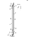
- 1 is an external perspective view of a flat cable including a transmission line according to a first embodiment of the invention. It is a disassembled perspective view which shows the structure of the main transmission line part which concerns on the 1st Embodiment of this invention. It is a disassembled plan view which shows the structure of the main transmission line part which concerns on the 1st Embodiment of this invention. It is sectional drawing which shows the structure of the main transmission line part which concerns on the 1st Embodiment of this invention.
- 1A and 1B are a side cross-sectional view and a plan cross-sectional view illustrating a component configuration of an electronic device according to a first embodiment of the present invention.
- FIG. 1 is an external perspective view of a flat cable including a transmission line according to the first embodiment of the invention.
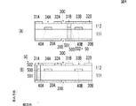
- FIG. 2 is an exploded perspective view showing the structure of the main transmission line section according to the first embodiment of the present invention.
- FIG. 3 is an exploded plan view showing the structure of the main transmission line section according to the first embodiment of the present invention.
- FIG. 4 is a cross-sectional view showing the structure of the main transmission line unit according to the first embodiment of the present invention.
- 4A is a cross-sectional view taken along the line AA shown in FIG. 3
- FIG. 4B is a cross-sectional view taken along the line BB shown in FIG.
- FIG. 1 shows the reference ground conductor side on which the connector is disposed as the upper surface
- the flat cable 60 includes a main transmission line 10, lead transmission lines 11A, 11B, 12A, and 12B, and connectors 61A1, 61A2, 61B1, and 61B2.
- the main transmission line 10 is flat and has a long shape. This long direction is the longitudinal direction of the main transmission line 10 and corresponds to the transmission direction of the high-frequency signal. Further, the direction parallel to the flat plate surface and perpendicular to the longitudinal direction (that is, the transmission direction) is the width direction.
- the main transmission line 10 corresponds to the “transmission line” and the “main line portion” of the present invention.
- the main transmission line 10 includes a dielectric body 110, reference ground conductors 20A and 20B, auxiliary ground conductors 30A and 30B, and signal conductors 40A and 40B.
- the dielectric element body 110 includes a first dielectric layer 111 and a second dielectric layer 112.
- the dielectric body 110 is a flexible flat plate having a predetermined thickness.
- the dielectric body 110 is long and is made of a flexible material such as polyimide or liquid crystal polymer.
- the first dielectric layer 111 and the second dielectric layer 112 may each be a laminate of a plurality of dielectric layers.
- the reference ground conductors 20 ⁇ / b> A and 20 ⁇ / b> B are arranged on one end surface (flat plate surface) of the dielectric body 110, in other words, on the exposed surface of the first dielectric layer 111.
- the reference ground conductors 20 ⁇ / b> A and 20 ⁇ / b> B are long solid conductors and have a shape extending in the same direction as the long direction of the dielectric body 110.
- the reference ground conductors 20A and 20B are arranged with a gap 200 in the width direction.
- the reference ground conductors 20A and 20B are made of a highly conductive material such as copper (Cu).
- the reference ground conductors 20A and 20B are ground conductors that mainly determine the characteristic impedance of the main transmission line 10 and the lead transmission lines 11A, 11B, 12A, and 12B.
- the signal conductors 40A and 40B and the reference ground conductors 20A and 20B are designed so that the characteristic impedance of the main transmission line 10 is 55 ⁇ , which is slightly higher than 50 ⁇ .
- the shapes of the auxiliary ground conductors 30A and 30B are adjusted so that the characteristic impedance of the main transmission line 10 is 50 ⁇ by the signal conductors 40A and 40B, the reference ground conductors 20A and 20B, and auxiliary ground conductors 30A and 30B described later.
- the auxiliary ground conductors 30A and 30B are formed on the other end surface (flat plate surface) of the dielectric body 110, in other words, on the exposed surface of the second dielectric layer 112.
- the auxiliary ground conductors 30 ⁇ / b> A and 30 ⁇ / b> B are elongated and have a shape that extends in the same direction as the longitudinal direction of the dielectric body 110.
- the auxiliary ground conductors 30A and 30B are arranged with a gap 300 in the width direction.
- the auxiliary ground conductor 30 ⁇ / b> A faces the reference ground conductor 20 ⁇ / b> A through the dielectric body 110.
- the auxiliary ground conductor 30B is opposed to the reference ground conductor 20B with the dielectric body 110 interposed therebetween.
- the auxiliary ground conductors 30A and 30B are also made of a highly conductive material such as copper (Cu).
- the auxiliary ground conductor 30A includes long conductors 31A and 32A and a bridge conductor 33A.
- the long conductors 31 ⁇ / b> A and 32 ⁇ / b> A have a long shape extending along the longitudinal direction of the dielectric body 110.
- the long conductors 31 ⁇ / b> A and 32 ⁇ / b> A are formed at a predetermined interval along the width direction of the dielectric body 110.
- the bridge conductor 33 ⁇ / b> A has a shape extending in the width direction of the dielectric body 110.
- a plurality of bridge conductors 33 ⁇ / b> A are formed at intervals along the longitudinal direction of the dielectric body 110.
- an opening 34A is formed between the bridge conductors 33A when viewed from a direction orthogonal to the flat plate surface (as viewed along the thickness direction).
- the auxiliary ground conductor 30A has a ladder shape extending in the longitudinal direction.
- the auxiliary ground conductor 30B includes long conductors 31B and 32B and a bridge conductor 33B.
- the long conductors 31 ⁇ / b> B and 32 ⁇ / b> B have a long shape extending along the longitudinal direction of the dielectric body 110.
- the long conductors 31 ⁇ / b> B and 32 ⁇ / b> B are formed at a predetermined interval along the width direction of the dielectric body 110.
- the bridge conductor 33 ⁇ / b> B has a shape extending in the width direction of the dielectric body 110.
- a plurality of bridge conductors 33 ⁇ / b> B are formed at intervals along the longitudinal direction of the dielectric body 110.
- an opening 34B is formed between the bridge conductors 33B when viewed from a direction orthogonal to the flat plate surface (as viewed along the thickness direction).
- the auxiliary ground conductor 30B has a ladder shape extending in the longitudinal direction.
- the interval in the transmission direction of the bridge conductors 33A and 33B of the auxiliary ground conductors 30A and 30B is designed so that no radiation noise is generated within the use band.
- the auxiliary ground conductors 30A and 30B are ground conductors that also function as shields. Further, as described above, the auxiliary ground conductors 30A and 30B are arranged, for example, for final adjustment so that the characteristic impedance of the main transmission line 10 becomes 50 ⁇ .
- the auxiliary ground conductor 30 ⁇ / b> A is connected to the reference ground conductor 20 ⁇ / b> A via a thickness direction connecting conductor 50 that penetrates the dielectric body 110 in the thickness direction.
- the auxiliary ground conductor 30B is connected to the reference ground conductor 20B through a thickness direction connecting conductor 50 that penetrates the thickness direction.
- the thickness direction connecting conductor 50 is formed at a plurality of locations.
- the thickness direction connecting conductor 50 includes an intermediate conductor pattern 500 and via conductors 501 and 502 as shown in FIG.
- the intermediate conductor pattern 500 is formed on the boundary surface between the first dielectric layer 111 and the second dielectric layer 112.
- the via conductor 501 has a shape penetrating the first dielectric layer 111.
- the via conductor 502 has a shape penetrating the second dielectric layer 112.
- the thickness direction connecting conductor 50 is provided at the intersection of the bridge conductor and the long conductor of each of the auxiliary ground conductors 30A and 30B. Further, the thickness direction connecting conductor 50 has a constant diameter. Accordingly, the auxiliary ground conductors 30A and 30B in the portion where the thickness direction connecting conductor 50 is provided project in the width direction (opening direction) correspondingly. Further, the signal conductors 40A and 40B have notches that become narrow in the width direction in correspondence with the protrusions of the thickness direction connecting conductor 50 and the auxiliary ground conductors 30A and 30B. The characteristic impedance of the main transmission line 10 is designed in consideration of this point.
- the thickness direction connecting conductors 50 are provided alternately one by one in the width direction at the intersections between the bridge conductors and the long conductors of the auxiliary ground conductors 30A and 30B. If two thickness direction connecting conductors 50 are provided in a certain width direction, the signal conductors 40A and 40B must be designed to be narrow in the width direction in a portion overlapping the bridge conductor. As a result, the transmission characteristics of the signal conductors 40A and 40B may be deteriorated. In order to avoid this, the main transmission line 10 must be widened. In the present embodiment, since only one thickness direction connecting conductor 50 is provided in a certain width direction, the width of the signal conductors 40A and 40B can be suppressed, and the width of the main transmission line 10 can be increased. There is no need to do.
- the thickness direction connecting conductors 50 are provided alternately one by one in the width direction at the intersections of the bridge conductors and the long conductors of the auxiliary ground conductors 30A and 30B, isolation between adjacent individual transmission units is provided. In addition, it is possible to secure isolation from external circuits. Further, the ground potentials of the auxiliary ground conductors 30A and 30B can be well balanced.
- the signal conductors 40A and 40B have a flat film shape and are formed between the first dielectric layer 111 and the second dielectric layer 112.
- the signal conductors 40 ⁇ / b> A and 40 ⁇ / b> B are arranged at a predetermined interval along the width direction of the dielectric body 110.
- the signal conductors 40A and 40B are also made of a highly conductive material such as copper (Cu).
- the signal conductor 40A is disposed so as to face the reference ground conductor 20A via the first dielectric layer 111 and to face the auxiliary ground conductor 30A via the second dielectric layer 112.
- the signal conductor 40A is located approximately at the center in the width direction of the reference ground conductor 20A, and is disposed at approximately the center in the width direction of the opening 34A of the auxiliary ground conductor 30A.
- the signal conductor 40B is disposed so as to face the reference ground conductor 20B via the first dielectric layer 111 and face the auxiliary ground conductor 30B via the second dielectric layer 112.
- the signal conductor 40B is positioned approximately at the center in the width direction of the reference ground conductor 20B, and is disposed at approximately the center in the width direction of the opening 34B of the auxiliary ground conductor 30B.
- the main transmission line 10 has a structure in which the first main line and the second main line are arranged with an interval in the width direction based on the single dielectric body 110.
- the first main line includes a reference ground conductor 20A, an auxiliary ground conductor 30A, a signal conductor 40A, and a dielectric element body 110.
- the second main line includes a reference ground conductor 20B, an auxiliary ground conductor 30B, a signal conductor 40B, and a dielectric body 110.
- the arrangement positions along the longitudinal direction of the bridge conductor 33A of the first main line and the bridge conductor 33B of the second main line are different. More specifically, the bridge conductor 33A of the first main line is disposed at an intermediate position between adjacent bridge conductors 33B in the second main line.
- the intermediate position between the adjacent bridge conductors is a portion where the distance from the bridge conductor is farthest, and the electric field strength and magnetic field strength due to the high-frequency signal are the largest.
- the maximum point of the electric field strength and the maximum point of the magnetic field strength by the high-frequency signal transmitted through the first main line, and the maximum point and the magnetic field strength of the electric field strength by the high-frequency signal transmitted through the second main line. are not aligned along the longitudinal direction. Thereby, the isolation of a 1st main line and a 2nd main line can be ensured highly, and the crosstalk of the high frequency signal which transmits a 1st main line, and the high frequency signal which transmits a 2nd main line can be suppressed. This is because the electric field distribution and magnetic field distribution of the high-frequency signal transmitted through the first and second main lines depend on the position and pattern of the bridge conductors 33A and 33B.
- the single dielectric element 110 is used in the present embodiment, it can be formed smaller than the case where the dielectric element 110 is used for each high-frequency signal. Further, by using the flat dielectric element 110, the transmission line can be made thinner than the coaxial cable.
- the reference ground conductors 20A and 20B by arranging the reference ground conductors 20A and 20B with the gap 200 in the width direction, it is possible to suppress the first main line and the second main line from being coupled via the ground. . Thereby, the isolation between a 1st main line and a 2nd main line can be ensured still higher.
- the positional relationship between the bridge conductors 33A and 33B is preferably set to an intermediate position along the longitudinal direction as in the present embodiment from the viewpoint of isolation, but the position along the longitudinal direction may be different. That's fine.
- the thickness direction connecting conductor 50 is preferably formed at least at a position where the long conductors 32A and 31B on the side where the first main line and the second main line are close to each other and the reference ground conductors 20A and 20B face each other. .
- the first main line and the second main line are separated by the thickness direction connecting conductor 50 connected to the ground potential, so that the first main line in the dielectric layer 111 and Electromagnetic field coupling with the second main line can be suppressed.
- the lead transmission lines 11 ⁇ / b> A and 11 ⁇ / b> B are connected to one end in the longitudinal direction of the main transmission line 10.
- the lead transmission lines 11A and 11B are arranged at a predetermined interval in the width direction.
- the lead transmission lines 12 ⁇ / b> A and 12 ⁇ / b> B are connected to the other end in the longitudinal direction of the main transmission line 10.
- the lead transmission lines 12A and 12B are arranged at a predetermined interval in the width direction.
- the lead-out transmission lines 11A and 12A are arranged at both ends in the longitudinal direction with the main transmission line 10 interposed therebetween.
- the lead transmission lines 11B and 12B are disposed at both ends in the longitudinal direction with the main transmission line 10 interposed therebetween.
- the lead transmission lines 11 A and 11 B are connected to the first main line of the main transmission line 10, and the lead transmission lines 12 A and 12 B are connected to the second main line of the main transmission line 10.
- the lead transmission lines 11A, 11B, 12A, 12B have the following structure.
- the lead transmission lines 11A, 11B, 12A, and 12B are composed of a dielectric element body in which a signal conductor is arranged at a predetermined position in the thickness direction using a reference ground conductor and an auxiliary ground conductor. It consists of a sandwiched structure.
- the signal conductors of the lead transmission lines 11A and 12A are connected to the signal conductor 40A of the main transmission line 10.
- the reference ground conductors of the lead transmission lines 11A and 12A are connected to the reference ground conductor 20A of the main transmission line 10.
- the auxiliary ground conductors of the lead transmission lines 11A and 12A are connected to the auxiliary ground conductor 30A of the main transmission line 10. The functions of the reference ground conductor and the auxiliary ground conductor are the same as described above.
- the signal conductors of the lead transmission lines 11B and 12B are connected to the signal conductor 40B of the main transmission line 10.
- the reference ground conductors of the lead transmission lines 11B and 12B are connected to the reference ground conductor 20B of the main transmission line 10.
- the auxiliary ground conductors of the lead transmission lines 11B and 12B are connected to the auxiliary ground conductor 30B of the main transmission line 10.
- the widths of the first main line and the second main line and the widths of the lead transmission lines 11A, 11B, 12A, and 12B are different, the widths of the first main line and the second main line and the lead transmission lines 11A, 11B, and 12A are different.
- 12B may be structured such that the distance between the long conductors of the auxiliary ground conductor (length in the width direction) gradually changes. Thereby, the transmission loss between the widths of the first main line and the second main line and the lead transmission lines 11A, 11B, 12A, 12B can be suppressed.
- the connector 61A1 is disposed at the end of the lead transmission line 11A (the end opposite to the main transmission line 10).
- the connector 61A2 is disposed at the end of the lead transmission line 12A (the end opposite to the main transmission line 10).
- the connector 61B1 is disposed at the end of the lead transmission line 11B (the end opposite to the main transmission line 10).
- the connector 61B2 is disposed at the end of the lead transmission line 12B (the end opposite to the main transmission line 10).
- the connectors 61A1 and 61B1 are arranged on one end side of the main transmission line 10, and 61A2 and 61B2 are arranged on the other end face side of the main transmission line 10.
- the connector 61A1 is electrically connected to the lead transmission line 11A
- the connector 61A2 is electrically connected to the lead transmission line 12A
- the connector 61B1 is electrically connected to the lead transmission line 11B
- the connector 61B2 is electrically connected to the lead transmission line 12B.
- coaxial type connectors can be used as the connectors 61A1, 61A2, 61B1, and 61B2 for example.
- a protective film (not shown) may be formed on both flat surfaces of the flat cable 60.
- a flat cable capable of transmitting these high-frequency signals with high isolation between a plurality of high-frequency signals can be formed small and thin.
- the flat cable 60 having such a structure is manufactured as follows, for example.
- the lead-out transmission lines 11A, 11B, 12A, and 12B are also formed integrally with the main transmission line 10.
- first, second, and third insulating films with a single-sided copper paste with a copper foil stretched over the entire surface of one side are prepared.
- a liquid crystal polymer is used as the insulating film.
- the reference ground conductors 20A and 20B are formed on one end face of the first insulating film by patterning.
- Signal conductors 40A and 40B are formed on the other end surface of the second insulating film by patterning.
- Auxiliary ground conductors 30A and 30B are formed by patterning on the other end surface side of the third insulating film. Then, the reference ground conductor 20A and the auxiliary ground conductor 30A are connected, and the first, second, and third insulating films are connected in the thickness direction so as to connect the reference ground conductor 20B and the auxiliary ground conductor 30B.
- a conductor 50 is formed.
- a through hole is formed by irradiating a laser beam from the side of the first, second, and third insulating films where the copper foil is not stretched, and the through hole is filled with a conductive paste.
- the thickness direction connecting conductor 50 can be formed.
- the reference ground conductor 20A and the auxiliary ground conductor 30A are opposed to each other with the signal conductor 40A interposed therebetween, and the reference ground conductor 20B and the auxiliary ground conductor 30B are opposed to each other with the signal conductor 40B interposed therebetween.
- a dielectric body 110 is formed by bonding a third insulating film.
- the connectors 61A1, 61A2, 61B1, 61B2 are installed on the lead transmission lines 11A, 11B, 12A, 12B arranged at both ends in the longitudinal direction of the flat cable 60.
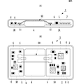
- FIG. 5A is a side cross-sectional view illustrating a component configuration of the portable electronic device according to the first embodiment of the present invention
- FIG. 5B is a plan cross-sectional view illustrating the component configuration of the portable electronic device. is there.
- the portable electronic device 1 includes a thin device casing 2.
- the device casing 2 mounted circuit boards 3A and 3B, which are circuit elements, and a battery pack 4 are arranged.
- a plurality of IC chips 5 and mounting components 6 are mounted on the surfaces of the mounting circuit boards 3A and 3B.
- the mounting circuit boards 3A and 3B and the battery pack 4 are installed in the equipment casing 2 so that the battery pack 4 is disposed between the mounting circuit boards 3A and 3B when the equipment casing 2 is viewed in plan.
- the device housing 2 is formed as thin as possible, the distance between the battery pack 4 and the device housing 2 is extremely narrow in the thickness direction of the device housing 2. Therefore, a coaxial cable cannot be arranged between them.
- the flat cable 60 shown in the present embodiment is arranged so that the thickness direction of the flat cable 60 and the thickness direction of the device housing 2 coincide with each other. A flat cable 60 can be passed between them. As a result, the mounted circuit boards 3A and 3B which are spaced apart from each other with the battery pack 4 disposed in the middle can be connected by the flat cable 60.
- connection position of the flat cable 60 to the mounting circuit boards 3A and 3B and the installation surface of the flat cable 60 of the battery pack 4 are different in the thickness direction of the device housing 2, and the flat cable 60 must be bent and connected. Even when it is necessary, by using the structure of this embodiment, it is possible to transmit a high-frequency signal while suppressing transmission loss.
- the area for transmitting the plurality of high-frequency signals can be reduced, and space can be saved. At this time, the transmission loss of each high-frequency signal can be reduced and transmitted.
- FIG. 6 is an exploded plan view showing the structure of the main transmission line according to the second embodiment of the present invention.
- the main transmission line 10 'of the present embodiment is different from the main transmission line 10 according to the first embodiment in the structure of the reference ground conductor and the auxiliary ground conductor, and the other configurations are the same. Therefore, only different points from the main transmission line 10 according to the first embodiment will be specifically described.
- the reference ground conductors 20A and 20B are connected by a connecting conductor portion 201.
- the connecting conductor portion 201 corresponds to the “first connecting conductor portion” of the present invention.
- the connecting conductor portion 201 is partially formed at a predetermined position along the longitudinal direction of the reference ground conductors 20A and 20B (the transmission direction of the high-frequency signal to be transmitted). In other words, the connecting conductor portion 201 is formed so as to partially fill the gap 200. It is sufficient that at least one connecting conductor portion 201 is formed.
- the gap 200 is secured while ensuring flexibility by the gap 200 not filled with the connecting conductor portion 201.
- the resonance frequency of the unnecessary high-frequency signal generated by providing can be shifted to the high frequency side. Thereby, transmission loss can be reduced.
- the auxiliary ground conductors 30 ⁇ / b> A and 30 ⁇ / b> B are connected by a connecting conductor portion 301.
- the connecting conductor portion 301 corresponds to the “second connecting conductor portion” of the present invention.
- the connecting conductor portion 301 is partially formed at a predetermined position along the longitudinal direction of the auxiliary ground conductors 30A and 30B. In other words, the connecting conductor portion 301 is formed so as to partially fill the gap 300. It is sufficient that at least one connecting conductor portion 301 is formed.
- the gap 300 is formed while ensuring flexibility by the gap 300 not filled with the connecting conductor portion 301.
- the resonance frequency of the unnecessary high-frequency signal generated by providing can be shifted to the high frequency side. Thereby, transmission loss can be reduced.
- the main transmission line 10 is viewed in plan so that the connection conductor portion 201 and the connection conductor portion 301 overlap with each other, and the connection conductor portions 201 and 301 along the longitudinal direction of the main transmission line 10. It is preferable to form the thickness direction connecting conductor 53 at a position where is formed.
- the thickness direction connecting conductor 53 connects the connecting conductor portions 201 and 301.
- the thickness direction connecting conductor 53 connects the reference ground conductor 20A at and near the position to which the connecting conductor portion 201 is connected and the auxiliary ground conductor 30A at and near the position to which the connecting conductor portion 301 is connected, or the connecting conductor portion 201. Is connected to the reference ground conductor 20B at and near the position where the connecting conductor portion 301 is connected and the auxiliary ground conductor 30B at and near the position where the connecting conductor portion 301 is connected.
- a plurality of the thickness direction connecting conductors 53 are provided at different positions along the longitudinal direction.
- the thickness direction connection conductor 53 it is possible to ensure isolation between the first main line and the second main line.
- opening 211 is so-called conductor non-forming portions in the connecting conductor portions 201 and 301.
- These openings 211 are so-called conductor non-forming portions in the connecting conductor portions 201 and 301.
- a decrease in flexibility due to the connecting conductor portions 201 and 301 can be mitigated.
- the magnetic coupling between the first main line and the second main line via the openings 34A and 34B provided in the auxiliary ground conductors 30A and 30B. can be weakened.
- the thickness direction connecting conductor 53 in a region sandwiched between the openings 211 and 311 and the signal conductors 40A and 40B.
- At least one of the connecting conductor portions 201 and 301 may be formed.
- FIG. 7 is an exploded plan view showing the structure of the main transmission line according to the third embodiment of the present invention.
- the main transmission line 10A of the present embodiment is different from the main transmission line 10 according to the first embodiment in the structure of the reference ground conductor, and the other configurations are the same. Therefore, only different points from the main transmission line 10 according to the first embodiment will be specifically described.
- the main transmission line 10 ⁇ / b> A includes a reference ground conductor 20.
- the reference ground conductor 20 is obtained by integrating the reference ground conductors 20A and 20B shown in the first embodiment. Even if it is such a structure, the effect similar to 1st Embodiment can be acquired. Furthermore, in the configuration of the present embodiment, it is not necessary to provide the gap 200, so that the formation of the reference ground conductor is facilitated.
- FIG. 8 is an exploded plan view showing the structure of the main transmission line section according to the fourth embodiment of the present invention.
- the main transmission line 10B of the present embodiment is different from the main transmission line 10A according to the third embodiment in the structure of the auxiliary ground conductor, and the other configurations are the same. Therefore, only different points from the main transmission line 10A according to the third embodiment will be specifically described.
- the auxiliary ground conductors 30A1 and 30A2 have a common long conductor 312 in the width direction opposite to each other shared by the first main line and the second main line.
- variety of the main transmission line 10 can be made narrower than the structure which does not use a common elongate conductor by the 1st main line and the 2nd main line.
- the thickness direction connecting conductor 50 provided on the long conductor of the portion shared by the first main line and the second main line has the bridge conductors 33A and 33B along the longitudinal direction. It is formed in the middle position of the arrangement position.
- the ground is installed at a position where the opening 34A of the first main line and the opening 34B of the second main line are adjacent to each other in the width direction. Accordingly, the isolation between the first main line and the second main line can be further increased, and crosstalk between the high-frequency signal transmitted through the first main line and the high-frequency signal transmitted through the second main line is further suppressed. it can.
- This arrangement structure of the thickness direction connection conductors 50 may be applied even when the long conductors on the side where the first main line and the second main line face each other are not shared, but the width of the long conductors is connected in the thickness direction. Since it is necessary to make it larger than the diameter of the conductor 50, the width of the main transmission line 10 will become wide. However, in the configuration of the present embodiment, the long conductor on the side where the first main line and the second main line face each other is shared. Therefore, even if the width of the long conductor is increased, the width of the main transmission line 10 can be reduced as much as possible, and this configuration works more effectively.
- FIG. 9 is an exploded plan view showing the structure of the main transmission line section according to the fifth embodiment of the present invention.
- the main transmission line 10C of the present embodiment is different from the main transmission line 10B according to the fourth embodiment in the structure of the auxiliary ground conductor, and the other configurations are the same. Therefore, only different points from the main transmission line 10B according to the fourth embodiment will be specifically described.
- the thickness direction connection conductor 50 is not provided at a position overlapping the long conductors 31An and 32Bn at both ends of the dielectric body 110 in the width direction.
- the width of the long conductors 31An and 32Bn can be reduced.
- the width of the signal conductors 40A and 40B can be increased and transmission loss can be reduced. Further, when the width of the dielectric body 110 is changed, the width of the dielectric body 110 can be reduced.
- the thickness direction connecting conductors 50 are disposed at both ends of the dielectric element body 110 in the width direction. By arranging such a thickness direction connection conductor 50, external interference between the first main line and the second main line can be suppressed.
- the width of the opening in the main transmission line is made constant has been shown.
- the width of the opening may be gradually increased from the end connected to the bridge conductor toward the center in the longitudinal direction of the opening.
- the example in which the width of the signal conductor of the main transmission line is made constant is shown.
- the width of the signal conductor in the portion facing the opening may be increased.
- the signal conductor is widened so as not to overlap the long conductor when the flat cable is viewed in the thickness direction. Thereby, the high frequency resistance of a signal conductor can be reduced and the conductor loss of a flat cable can be reduced.
- FIG. 10 is an external perspective view of a flat cable including a transmission line according to the sixth embodiment of the present invention.
- FIG. 11 is an exploded plan view showing the structure of a flat cable lead-out transmission line according to the sixth embodiment of the present invention.
- the structure of the outgoing transmission line of the one end of the flat cable in the elongate direction is illustrated, but the outgoing transmission line of the other end also has the same structure.
- the flat cable 60D shown in this embodiment has connectors 61A1, 61A2, 61B1, and 61B2 arranged on the auxiliary ground conductor side, and the reference ground conductor is a signal conductor. It is arrange
- the flat cable 60D includes a main transmission line 10D, lead transmission lines 11AD, 11BD, 12AD, 12BD, and connectors 61A1, 61A2, 61B1, 61B2.
- the main transmission line 10D has an auxiliary ground disposed on the connector side of the signal conductor and a reference ground disposed on the opposite side of the signal conductor connector. Consists of structure.
- the lead transmission lines 11BD and 12BD have a long shape extending in the same direction as the long direction of the main transmission line 10D, similarly to the lead transmission lines 11B and 12B shown in the first embodiment. These lead transmission lines 11BD and 12BD correspond to the “first lead transmission line” of the present invention.
- the lead-out transmission lines 11AD and 12AD have a linear part ReS extending in the same direction as the longitudinal direction of the main transmission line 10D and a curved part ReC that curves in a direction different from the longitudinal direction. These lead transmission lines 11AD and 12AD correspond to the “second lead transmission line” of the present invention.
- the lead-out transmission line 11BD includes a long dielectric element body 110BN extending along the long direction of the main transmission line 10D.
- One end of the dielectric body 110BN in the longitudinal direction is connected to the dielectric body 110 constituting the main line conductor.
- the other end of the dielectric body 110BN is partially widened. That is, the length of the other end of the dielectric element body 110BN in the short side direction is longer than that of the dielectric element body 110 side.
- an auxiliary ground conductor 30BN, a signal conductor 40BN, and a reference ground conductor 20BN are arranged at intervals along the thickness direction.
- the auxiliary ground conductor 30BN includes long conductors 31BN and 32BN extending along the long direction of the dielectric body 110BN.
- the long conductor 31BN is connected to the long conductor 31B of the main transmission line 10D, and the long conductor 32BN is connected to the long conductor 32B of the main transmission line 10D.
- the long conductors 31BN and 32BN are formed near both ends in the short direction of the dielectric element body 110BN.
- the long conductors 31BN and 32BN are connected by a plurality of bridge conductors 33BN disposed at intervals along the extending direction.
- the long conductors 31BN and 32BN are connected by a connector connecting conductor 43BN at the other end of the dielectric element body 110BN (the end opposite to the side connected to the dielectric element body 110).
- the connector connecting conductor 43BN is formed over substantially the entire wide portion at the other end of the dielectric element body 110BN, and an opening in which no conductor is formed is provided at the center.
- a connector connecting conductor 42BN is formed in the center of the opening so as not to be connected to the connector connecting conductor 43BN.
- the signal conductor 40BN has a shape extending along the longitudinal direction of the dielectric element body 110BN, and is disposed at the center position in the short direction of the dielectric element body 110BN.
- the signal conductor 40BN is connected to the signal conductor 40B of the main transmission line 10D.
- the signal conductor 40BN is arranged so as not to overlap the long conductors 31BN and 32BN of the auxiliary ground conductor 30BN in plan view of the dielectric body 110BN.
- the signal conductor 40BN is connected to the connector connecting conductor 41BN at the other end of the dielectric body 110BN.
- the connector connecting conductor 41BN is connected to the connector connecting auxiliary conductor 42BN through the thickness direction connecting conductor 50.
- the reference ground conductor 20BN has a shape extending along the longitudinal direction of the dielectric body 110BN.
- the width (length in the short direction) of the reference ground conductor 20BN is substantially the same as the width (length in the short direction) of the dielectric element body 110BN.
- the reference ground conductor 20BN is connected to the long conductors 31BN and 32BN of the auxiliary ground conductor 30BN through the thickness direction connecting conductor 50.
- the reference ground conductor 20BN is connected to the connector connecting conductor 44BN at the other end of the dielectric body 110BN.
- the connector connecting conductor 44BN is connected to the connector connecting auxiliary conductor 41BN via the thickness direction connecting conductor 50.
- the lead-out transmission line 11AD has an elongated shape having a linear part ReS extending in the same direction as the longitudinal direction of the main transmission line 10D and a curved part ReC curved in a direction different from the longitudinal direction.
- a dielectric body 110AN is provided. One end in the longitudinal direction of the dielectric body 110AN is connected to the dielectric body 110 constituting the main line conductor. The other end of the dielectric body 110AN is partially wide. That is, the length of the other end of the dielectric body 110AN in the short direction is longer than that of the dielectric body 110 side.
- an auxiliary ground conductor 30AN, a signal conductor 40AN, and a reference ground conductor 20AN are arranged at intervals along the thickness direction.
- the auxiliary ground conductor 30AN includes long conductors 31AN and 32AN.
- the long conductors 31AN and 32AN have a shape extending along the long direction of the dielectric body 110AN in the straight portion ReS, and from a shape extending along the curved shape of the dielectric body 110AN in the curved portion ReC. Become.
- the long conductor 31AN is connected to the long conductor 31A of the main transmission line 10D
- the long conductor 32AN is connected to the long conductor 32A of the main transmission line 10D.
- the long conductors 31AN and 3ABN are formed near both ends of the dielectric body 110AN in the short direction.
- the long conductors 31AN and 32AN are connected by a plurality of bridge conductors 33AN arranged at intervals along the extending direction.
- the long conductors 31AN and 32AN are connected by a connector connecting conductor 43AN at the other end of the dielectric body 110AN (the end opposite to the side connected to the dielectric body 110).
- the connector connecting conductor 43AN is formed over substantially the entire wide portion of the other end of the dielectric body 110AN, and an opening in which no conductor is formed is provided at the center.
- a connector connecting conductor 42AN is formed in the center of the opening so as not to be connected to the connector connecting conductor 43AN.
- the signal conductor 40AN has a shape that extends along the longitudinal direction of the dielectric body 110AN in the straight portion ReS, and a shape that extends along the curved shape of the dielectric body 110AN in the curved portion ReC.
- the signal conductor 40AN is arranged at the center position in the short direction of the dielectric body 110AN.
- the signal conductor 40AN is connected to the signal conductor 40A of the main transmission line 10D.
- the signal conductor 40AN is disposed so as not to overlap with the long conductors 31AN and 32AN of the auxiliary ground conductor 30AN in a plan view of the dielectric body 110AN.
- the signal conductor 40AN is connected to the connector connecting conductor 41AN at the other end of the dielectric body 110AN.
- the connector connecting conductor 41AN is connected to the connector connecting auxiliary conductor 42AN through the thickness direction connecting conductor 50.
- the reference ground conductor 20AN has a shape extending along the longitudinal direction of the dielectric body 110AN in the straight portion ReS, and has a shape extending along the curved shape of the dielectric body 110AN in the curved portion ReC.
- the width (length in the short direction) of the reference ground conductor 20AN is substantially the same as the width (length in the short direction) of the dielectric body 110AN.
- the reference ground conductor 20AN is connected to the long conductors 31AN and 32AN of the auxiliary ground conductor 30AN through the thickness direction connecting conductor 50 only at the straight line portion ReS.
- the reference ground conductor 20AN is connected to the connector connecting conductor 44AN at the other end of the dielectric body 110AN.
- the connector connecting conductor 44AN is connected to the connector connecting auxiliary conductor 41AN via the thickness direction connecting conductor 50.
- the connectors 61B1 and 61B2 of the linear lead transmission lines 11BD and 12BD are first connected (fixed) to the mounting circuit board, and the flat cable 60D is mounted. Secure to the circuit board. Thereby, the flat cable 60D can be temporarily fixed to the mounting circuit board.
- the connectors 61A1 and 61A2 of the lead transmission lines 11AD and 12AD having the curved portion ReC are connected (fixed) to the mounting circuit board.
- the lead transmission lines 11AD and 12AD can be provided with a degree of freedom for handling. Thereby, even if there are many connector connection locations, the connector can be easily connected (fixed) to the mounting circuit board.
- the bending direction ReC since the bending direction ReC is not provided with the thickness direction connection conductor 50, the bending portion ReC has higher flexibility than the straight portion ReS. Therefore, the connector can be more easily connected (fixed) to the mounting circuit board. In addition, a change in characteristic impedance due to expansion / contraction of the bending portion ReC can be suppressed.
- one of the two lead transmission lines connected to one end in the longitudinal direction of the main transmission line 10D has a linear structure with relatively low flexibility, and the other relatively Although a structure having a highly flexible curved portion is provided, when three or more lead transmission lines are provided, at least one linear structure and a structure having a curved portion may be provided.
- the linear distance from the main transmission line 10D to the connector is the same in the transmission lines 11AD and 11BD and the same in the transmission lines 12AD and 12BD in the state where no external force is applied. Indicated. However, this linear distance may be different.
Landscapes
- Engineering & Computer Science (AREA)
- Microelectronics & Electronic Packaging (AREA)
- Physics & Mathematics (AREA)
- Electromagnetism (AREA)
- Waveguides (AREA)
- Insulated Conductors (AREA)
- Structure Of Printed Boards (AREA)
Abstract
A principal transmission line (10) is equipped with a long dielectric element (110). Long signal conductors (40A, 40B) are positioned inside the dielectric element (110) with intervals interposed therebetween in the widthwise direction. A reference ground conductor (20A) and an auxiliary ground conductor (30A) are positioned so as to sandwich the signal conductor (40A) therebetween in the thickness direction thereof. A reference ground conductor (20B) and an auxiliary ground conductor (30B) are positioned so as to sandwich the signal conductor (40B) therebetween in the thickness direction thereof. The auxiliary ground conductor (30A) is equipped with long conductors (31A, 32A) and a bridge conductor (33A), while the auxiliary ground conductor (30B) is equipped with long conductors (31B, 32B) and a bridge conductor (33B). The bridge conductors (33A, 33B) are located at different positions in the lengthwise direction.
Description
本発明は、高周波信号を伝送する薄型の伝送線路および当該伝送線路を備える電子機器に関するものである。
The present invention relates to a thin transmission line that transmits a high-frequency signal, and an electronic device including the transmission line.
現在、高周波信号を伝送する高周波伝送線路として、特許文献1に示すようなフラットケーブルを用いることが注目されている。フラットケーブルは、幅が同軸ケーブルよりも広いものの薄型にできるため、端末筐体内に薄い隙間しかないような場合に、特に有用である。また、フラットケーブルは、可撓性を有する誘電体素体を基材としているので、柔軟性があり、湾曲や屈曲させた引き回しを容易に行うことができる。
At present, the use of a flat cable as shown in Patent Document 1 is drawing attention as a high-frequency transmission line for transmitting a high-frequency signal. The flat cable is particularly useful when there is only a thin gap in the terminal housing because the flat cable can be made thinner but wider than the coaxial cable. Further, since the flat cable has a flexible dielectric body as a base material, it is flexible and can be easily bent and bent.
特許文献1に記載のフラットケーブルは、基本的な構造として、トリプレート型のストリップライン構造を有している。
The flat cable described in Patent Document 1 has a triplate stripline structure as a basic structure.
特許文献1に示すようなフラットケーブルは、可撓性を有し絶縁性を有する平板状の誘電体素体を備える。誘電体素体は、一直線状に延びる長尺形状である。誘電体素体の厚み方向に直交する一方面には、基準グランド導体が配設されている。基準グランド導体は、基材シートの第2面を略全面で覆う、所謂ベタ導体パターンである。
A flat cable as shown in Patent Document 1 includes a flat dielectric body having flexibility and insulation. The dielectric body has a long shape extending in a straight line. A reference ground conductor is disposed on one surface orthogonal to the thickness direction of the dielectric body. The reference ground conductor is a so-called solid conductor pattern that covers substantially the entire second surface of the base sheet.
基材シートの一方面に対向する他方面には、補助グランド導体が配設されている。補助グランド導体は、長手方向に沿って延びる形状の長尺導体を、長手方向および厚み方向に直交する幅方向の両端に備える。二本の長尺導体は、幅方向に延びる形状からなるブリッジ導体によって接続されている。ブリッジ導体は、長手方向に沿って所定間隔をおいて配置されている。これにより、補助グランド導体は、所定の開口長からなる開口部が長手方向に沿って配列形成された形状からなる。
An auxiliary ground conductor is disposed on the other surface facing the one surface of the base sheet. The auxiliary ground conductor includes long conductors extending along the longitudinal direction at both ends in the width direction orthogonal to the longitudinal direction and the thickness direction. The two long conductors are connected by a bridge conductor having a shape extending in the width direction. The bridge conductors are arranged at a predetermined interval along the longitudinal direction. Thus, the auxiliary ground conductor has a shape in which openings having a predetermined opening length are arrayed along the longitudinal direction.
誘電体素体の厚み方向の中間には、所定幅で所定厚みの信号導体が形成されている。信号導体は、補助グランド導体の長尺導体部および基準グランド導体と平行な方向に伸延する長尺状からなる。信号導体は、誘電体素体の幅方向の略中央に形成されている。
A signal conductor having a predetermined width and a predetermined thickness is formed in the middle of the dielectric body in the thickness direction. The signal conductor has a long shape extending in a direction parallel to the long conductor portion of the auxiliary ground conductor and the reference ground conductor. The signal conductor is formed at substantially the center in the width direction of the dielectric body.
このような構成により、フラットケーブルを平面視すると(一方面および他方面に直交する方向から見ると)、信号導体は、補助グランド導体に対して、ブリッジ導体で重なり合うだけで、他の領域では開口部内となるように配置される。
With this configuration, when the flat cable is viewed in plan (viewed from the direction orthogonal to the one side and the other side), the signal conductor only overlaps with the auxiliary ground conductor by the bridge conductor, and is open in other areas. Arranged to be inside the department.
しかしながら、現在、2種類の高周波信号を平行して伝送することが可能な伝送線路が要求されている。上述の特許文献1に記載のフラットケーブルを用いた場合、平行して伝送する高周波信号の数の分だけフラットケーブルを必要とする。したがって、これらを平行に並べて配置しなければならず、スペースを必要としてしまう。
However, there is currently a demand for a transmission line that can transmit two types of high-frequency signals in parallel. When the flat cable described in Patent Document 1 is used, as many flat cables as the number of high-frequency signals transmitted in parallel are required. Therefore, these must be arranged in parallel, and space is required.
また、単に、上述の特許文献1に記載の伝送線路の構造を一つの誘電体素体に並べて配置する場合、伝送方向に沿った開口部の位置が、隣り合う伝送線路間で一致する。この場合、それぞれの伝送線路を伝送する高周波信号による電界や磁界の放射が大きな位置は、隣り合う伝送線路同士で一致する。したがって、隣り合う伝送線路間でのアイソレーションが確保できず、それぞれの伝送線路を伝送する高周波信号同士がクロストークしてしまう。
Also, when the transmission line structure described in Patent Document 1 is simply arranged side by side on a single dielectric element body, the positions of the openings along the transmission direction coincide between adjacent transmission lines. In this case, the positions where the radiation of the electric field or magnetic field by the high-frequency signal transmitted through each transmission line is large coincide with each other in the adjacent transmission lines. Therefore, isolation between adjacent transmission lines cannot be ensured, and high-frequency signals transmitted through the respective transmission lines will crosstalk.
特に、フラットケーブルからなる伝送線路を小型化しようとすると、隣り合う伝送線路間の間隔が狭くなり、よりアイソレーションが低下して、クロストークが起きやすくなる。
Especially, when trying to reduce the size of a transmission line made of a flat cable, the interval between adjacent transmission lines becomes narrower, the isolation is further lowered, and crosstalk is likely to occur.
したがって、本発明の目的は、複数の高周波信号間のアイソレーションを高く確保した状態でこれらの高周波信号を伝送することが可能な伝送線路を小型且つ薄型に形成することである。
Therefore, an object of the present invention is to form a transmission line that can transmit these high-frequency signals in a small and thin state while ensuring high isolation between the plurality of high-frequency signals.
この発明の伝送線路は、誘電体素体、信号導体、基準グランド導体、補助グランド導体、厚み方向接続導体を備える。誘電体素体は、平板状であって所定厚みを有する。信号導体は、誘電体素体の内部に配置され、所定の伝送方向に沿って伸延する形状からなる。基準グランド導体は、誘電体素体の厚み方向の一方端面に配置されている。補助グランド導体は、誘電体素体の厚み方向の他方端面に配置されている。厚み方向接続導体は、基準グランド導体と補助グランド導体とを貫通して基準グランド導体と補助グランド導体とを接続する。
The transmission line of the present invention includes a dielectric body, a signal conductor, a reference ground conductor, an auxiliary ground conductor, and a thickness direction connecting conductor. The dielectric element body has a flat plate shape and a predetermined thickness. The signal conductor is arranged inside the dielectric element body and has a shape extending along a predetermined transmission direction. The reference ground conductor is disposed on one end face in the thickness direction of the dielectric element body. The auxiliary ground conductor is disposed on the other end surface in the thickness direction of the dielectric element body. The thickness direction connection conductor passes through the reference ground conductor and the auxiliary ground conductor and connects the reference ground conductor and the auxiliary ground conductor.
補助グランド導体は、伝送方向に伸延し、伝送方向に直交する方向に所定間隔をおいて配置される第1長尺導体および第2長尺導体を備える。補助グランド導体は、第1長尺導体と第2長尺導体を伝送方向に所定間隔をおいて接続するブリッジ導体を備える。基準グランド導体と補助グランド導体と信号導体との組による個別伝送部は、誘電体素体に対して、伝送方向に直交する方向に沿って複数配置されている。隣り合う個別伝送部のブリッジ導体は、伝送方向に沿った位置が異なっている。
The auxiliary ground conductor includes a first long conductor and a second long conductor that extend in the transmission direction and are arranged at a predetermined interval in a direction orthogonal to the transmission direction. The auxiliary ground conductor includes a bridge conductor that connects the first long conductor and the second long conductor at a predetermined interval in the transmission direction. A plurality of individual transmission units each including a pair of a reference ground conductor, an auxiliary ground conductor, and a signal conductor are arranged along a direction orthogonal to the transmission direction with respect to the dielectric body. The bridge conductors of adjacent individual transmission units differ in position along the transmission direction.
この構成では、隣り合う個別伝送部の電界および磁界の放射の極大点の伝送方向に沿った位置は、異なる。したがって、それぞれの個別伝送部を伝送する高周波信号同士が電磁界結合し難い。これにより、隣り合う個別伝送部間でのアイソレーションを高く確保できる。
In this configuration, the positions along the transmission direction of the maximal points of the electric field and magnetic field radiation of the adjacent individual transmission units are different. Therefore, it is difficult for the high frequency signals transmitted through the individual transmission units to be electromagnetically coupled to each other. Thereby, it is possible to ensure high isolation between adjacent individual transmission units.
また、この発明の伝送線路では、次の構成であることが好ましい。ある個別伝送部のブリッジ導体の伝送方向に沿った位置は、当該個別伝送部に隣り合う個別伝送部の伝送方向に隣り合うブリッジ導体の配置位置同士の略中央である。
Also, the transmission line of the present invention preferably has the following configuration. The position along the transmission direction of the bridge conductor of an individual transmission unit is substantially the center between the arrangement positions of the bridge conductors adjacent to each other in the transmission direction of the individual transmission unit adjacent to the individual transmission unit.
この構成では、隣り合う個別伝送部同士が最も電磁界結合し難い。これにより、隣り合う個別伝送部間でのアイソレーションをさらに高く確保できる。
In this configuration, adjacent individual transmission units are most unlikely to be electromagnetically coupled. Thereby, the isolation between adjacent individual transmission parts can be further ensured.
また、この発明の伝送線路では、次の構成であることが好ましい。厚み方向導体は、少なくとも、隣り合う個別伝送部同士における互いに対向する長尺導体と基準グランド導体とが厚み方向に沿って重なるように形成されている。
Also, the transmission line of the present invention preferably has the following configuration. The thickness direction conductor is formed such that at least the long conductors facing each other and the reference ground conductor in the adjacent individual transmission units overlap in the thickness direction.
この構成では、隣り合う個別伝送部の信号導体間に厚み方向導体が形成されているので、誘電体素体内での伝送方向に直交する方向に沿った電磁界結合を抑制できる。
In this configuration, since the thickness direction conductor is formed between the signal conductors of the adjacent individual transmission units, it is possible to suppress electromagnetic field coupling along the direction orthogonal to the transmission direction in the dielectric body.
また、この発明の伝送線路では、隣り合う個別伝送部の基準グランド導体は一体化されていることが好ましい。
In the transmission line of the present invention, it is preferable that the reference ground conductors of the adjacent individual transmission units are integrated.
この構成では、隣り合う個別伝送部の基準グランド導体を分離する導体非形成部が省略されるので、伝送線路の幅を狭くすることができる。または、伝送線路の幅を広くしなくても、信号導体の幅を広く設計することが可能になり伝送特性が向上する。
In this configuration, since the conductor non-forming portion that separates the reference ground conductors of the adjacent individual transmission portions is omitted, the width of the transmission line can be reduced. Alternatively, the width of the signal conductor can be designed wider without increasing the width of the transmission line, and the transmission characteristics are improved.
また、この発明の伝送線路では、隣り合う個別伝送部の基準グランド導体は所定の間隔をおいて分離されている。
Further, in the transmission line of the present invention, the reference ground conductors of adjacent individual transmission units are separated with a predetermined interval.
この構成では、基準グランド導体を介したクロストークを抑制できる。
In this configuration, crosstalk via the reference ground conductor can be suppressed.
また、この発明の伝送線路では、隣り合う個別伝送部の隣り合う第1長尺導体と第2長尺導体は一体化されている。
Further, in the transmission line of the present invention, the adjacent first long conductor and the second long conductor of the adjacent individual transmission units are integrated.
この構成では、隣り合う個別伝送部の長尺導体を分離する導体非形成部が省略されるので、伝送線路の幅を狭くすることができる。または、伝送線路の幅を広くしなくても、信号導体の幅を広く設計することが可能になり伝送特性が向上する。
In this configuration, the conductor non-forming portion that separates the long conductors of the adjacent individual transmission portions is omitted, so that the width of the transmission line can be reduced. Alternatively, the width of the signal conductor can be designed wider without increasing the width of the transmission line, and the transmission characteristics are improved.
また、この発明の伝送線路では、厚み方向導体は、一体化された第1長尺導体および第2長尺導体と、基準グランド導体とが厚み方向に沿って重なる位置のみに形成されていることが好ましい。
In the transmission line of the present invention, the thickness direction conductor is formed only at a position where the integrated first and second long conductors and the reference ground conductor overlap in the thickness direction. Is preferred.
この構成では、隣り合う個別伝送部における互いに対向していない長尺導体の幅を狭くできる。これにより、伝送線路の幅を変えることなく、第1、第2長尺導体とブリッジ導体で囲まれる開口部の面積を広くすることができる。したがって、信号導体の幅を広くでき、伝送損失を低減できる。
In this configuration, the width of the long conductors that are not facing each other in the adjacent individual transmission units can be reduced. Accordingly, the area of the opening surrounded by the first and second long conductors and the bridge conductor can be increased without changing the width of the transmission line. Therefore, the width of the signal conductor can be increased and transmission loss can be reduced.
また、この発明の伝送線路は、次の構成であってもよい。伝送線路は、上述のいずれかに記載の伝送線路を主伝送線路部とし、該主伝送線路部の両端に接続し、個別伝送部毎に設けられた引き出し伝送線路をさらに備える。主伝送線路部の一方端に接続する複数の引き出し伝送線路は、第1、第2引き出し伝送線路を備える。第1引き出し伝送線路は、主伝送線路部の伸延方向に沿って伸延し、主伝送線路部と同じ導体の構成からなる。第2引き出し伝送線路は、主伝送線路部の伸延方向に沿って伸長し主伝送線路部と同じ導体構成からなる直線部、および、該直線部と異なる方向に湾曲する形状からなる湾曲部を備える。
Further, the transmission line of the present invention may have the following configuration. The transmission line further includes a lead transmission line provided for each individual transmission unit, with the transmission line described in any of the above as a main transmission line unit, connected to both ends of the main transmission line unit. The plurality of lead transmission lines connected to one end of the main transmission line portion include first and second lead transmission lines. The first lead transmission line extends along the extending direction of the main transmission line part and has the same conductor configuration as the main transmission line part. The second lead-out transmission line includes a straight portion that extends along the extending direction of the main transmission line portion and has the same conductor configuration as the main transmission line portion, and a curved portion that has a shape that curves in a direction different from the straight portion. .
この構成では、主伝送線路部の一方端に接続される複数の引き出し伝送線路部の1つが取り回しのための自由度を有するので、実装回路基板に伝送線路を接続する際に、接続しやすい。
In this configuration, since one of the plurality of lead transmission line portions connected to one end of the main transmission line portion has a degree of freedom for routing, it is easy to connect when connecting the transmission line to the mounting circuit board.
また、この発明の伝送線路では、第2引き出し伝送線路の湾曲部は、補助グランド導体、信号導体、基準グランド導体が互いに接続することなく厚み方向に沿って配置されている構造であることが好ましい。
In the transmission line of the present invention, the curved portion of the second lead transmission line preferably has a structure in which the auxiliary ground conductor, the signal conductor, and the reference ground conductor are arranged along the thickness direction without being connected to each other. .
この構成では、湾曲部に厚み方向接続導体が配置されず、湾曲部の伸縮性が向上する。
In this configuration, the thickness direction connecting conductor is not disposed in the curved portion, and the stretchability of the curved portion is improved.
また、この発明の伝送線路では、間隔をおいて分離されている隣り合う個別伝送部の基準グランド導体は、第1連結導体部によって部分的に接続されていることが好ましい。
Further, in the transmission line of the present invention, it is preferable that the reference ground conductors of the adjacent individual transmission parts separated at intervals are partially connected by the first connecting conductor part.
また、この発明の伝送線路では、個別伝送部毎に分離された補助グランド導体は、第2連結導体部によって部分的に接続されていることが好ましい。
In the transmission line of the present invention, it is preferable that the auxiliary ground conductor separated for each individual transmission part is partially connected by the second connecting conductor part.
これらの構成では、個別伝送部間にできた空隙による不要な高周波信号の周波数を高周波数化でき、伝送損失を低減させることができる。
These configurations can increase the frequency of unnecessary high-frequency signals due to the gaps formed between the individual transmission units, thereby reducing transmission loss.
また、この発明の伝送線路では、第1連結導体部と第2連結導体部の少なくともいずれか一方に、導体の非形成部が備えられていることが好ましい。
Further, in the transmission line of the present invention, it is preferable that at least one of the first connection conductor portion and the second connection conductor portion is provided with a conductor non-formation portion.
この構成では、フレキシブル性を向上させることができる。
This configuration can improve flexibility.
また、この発明の伝送線路では、第1連結導体部と第2連結導体部、または、基準グランド導体における第1連結導体部が接続する位置と補助グランド導体における第2連結導体部が接続する位置には、厚み方向に伸延する接続導体が形成されていることが好ましい。
In the transmission line of the present invention, the position where the first connection conductor portion and the second connection conductor portion or the first connection conductor portion of the reference ground conductor is connected to the position of the second connection conductor portion of the auxiliary ground conductor is connected. It is preferable that a connection conductor extending in the thickness direction is formed.
この構成では、個別伝送部間のアイソレーションを、より高く確保することができる。
In this configuration, it is possible to secure higher isolation between the individual transmission units.
また、この発明の伝送線路では、平面視で、第1連結導体部と第2連結導体部の少なくともいずれか一方に設けられた導体の非形成部と信号導体との間に、基準グランドと補助グランド導体とを接続する厚み方向接続導体が形成されていることが好ましい。
In the transmission line according to the present invention, the reference ground and the auxiliary are provided between the non-formation portion of the conductor provided in at least one of the first connection conductor portion and the second connection conductor portion and the signal conductor in plan view. It is preferable that a thickness direction connecting conductor for connecting the ground conductor is formed.
この構成では、第1、第2連結導体部に開口部を設けたことによって個別伝送線路間のアイソレーションが低下することを抑制できる。
In this configuration, it is possible to suppress a decrease in isolation between the individual transmission lines by providing the first and second connecting conductor portions with openings.
また、この発明は、電子機器に関するのであり、次の構成であることを特徴としている。電子機器は、上述のいずれかに記載の伝送線路と、伝送線路によって接続される複数の回路要素と、当該回路要素が内蔵される筐体と、を備えている。
Further, the present invention relates to an electronic device and is characterized by the following configuration. An electronic device includes any of the transmission lines described above, a plurality of circuit elements connected by the transmission lines, and a housing in which the circuit elements are built.
この構成では、上述の伝送線路を用いた電子機器を示している。上述の伝送線路を用いることで、伝送する複数の伝送線路(個別伝送部)間のアイソレーションを高く確保できるので、複数の回路要素間で複数種類の高周波信号を伝送する場合に、伝送損失を低減することができる。
In this configuration, an electronic device using the above-described transmission line is shown. By using the above-mentioned transmission line, it is possible to ensure high isolation between a plurality of transmission lines (individual transmission units) to be transmitted. Therefore, when a plurality of types of high-frequency signals are transmitted between a plurality of circuit elements, transmission loss is reduced. Can be reduced.
この発明によれば、複数の高周波信号間のアイソレーションを高く確保した状態でこれらの高周波信号を伝送することが可能な伝送線路を小型且つ薄型に形成できる。
According to the present invention, a transmission line capable of transmitting these high-frequency signals in a state where high isolation between a plurality of high-frequency signals is ensured can be formed small and thin.
本発明の第1の実施形態に係る伝送線路について、図を参照して説明する。図1は、発明の第1の実施形態に係る伝送線路を含むフラットケーブルの外観斜視図である。図2は、本発明の第1の実施形態に係る主伝送線路部の構造を示す分解斜視図である。図3は、本発明の第1の実施形態に係る主伝送線路部の構造を示す分解平面図である。図4は、本発明の第1の実施形態に係る主伝送線路部の構造を示す断面図である。図4(A)は、図3に示すA-A断面図であり、図4(B)は図3に示すB-B断面図である。
The transmission line according to the first embodiment of the present invention will be described with reference to the drawings. FIG. 1 is an external perspective view of a flat cable including a transmission line according to the first embodiment of the invention. FIG. 2 is an exploded perspective view showing the structure of the main transmission line section according to the first embodiment of the present invention. FIG. 3 is an exploded plan view showing the structure of the main transmission line section according to the first embodiment of the present invention. FIG. 4 is a cross-sectional view showing the structure of the main transmission line unit according to the first embodiment of the present invention. 4A is a cross-sectional view taken along the line AA shown in FIG. 3, and FIG. 4B is a cross-sectional view taken along the line BB shown in FIG.
なお、図1は、コネクタが配設されている基準グランド導体側を上面として記載し、図2以降はコネクタが配設されていない補助グランド導体側を上面として記載している。
Note that FIG. 1 shows the reference ground conductor side on which the connector is disposed as the upper surface, and FIG.
フラットケーブル60は、主伝送線路10、引き出し伝送線路11A,11B,12A,12B、コネクタ61A1,61A2,61B1,61B2を備える。主伝送線路10は、平板状で且つ長尺状からなる。この長尺方向が主伝送線路10の長手方向であり、高周波信号の伝送方向に相当する。また、平板面に平行で長尺方向(すなわち、伝送方向)に直交する方向が幅方向である。主伝送線路10は、本発明の「伝送線路」および「主線路部」に相当する。
The flat cable 60 includes a main transmission line 10, lead transmission lines 11A, 11B, 12A, and 12B, and connectors 61A1, 61A2, 61B1, and 61B2. The main transmission line 10 is flat and has a long shape. This long direction is the longitudinal direction of the main transmission line 10 and corresponds to the transmission direction of the high-frequency signal. Further, the direction parallel to the flat plate surface and perpendicular to the longitudinal direction (that is, the transmission direction) is the width direction. The main transmission line 10 corresponds to the “transmission line” and the “main line portion” of the present invention.
図2に示すように、主伝送線路10は、誘電体素体110、基準グランド導体20A,20B、補助グランド導体30A,30B、信号導体40A,40Bを備える。
As shown in FIG. 2, the main transmission line 10 includes a dielectric body 110, reference ground conductors 20A and 20B, auxiliary ground conductors 30A and 30B, and signal conductors 40A and 40B.
誘電体素体110は、第1誘電体層111と第2誘電体層112とからなる。誘電体素体110は、所定の厚みを有する可撓性の平板である。誘電体素体110は、長尺状であり、例えば、ポリイミドや液晶ポリマ等の可撓性を有する素材からなる。なお、第1誘電体層111と第2誘電体層112はそれぞれ複数の誘電体層を積層したものであってもよい。
The dielectric element body 110 includes a first dielectric layer 111 and a second dielectric layer 112. The dielectric body 110 is a flexible flat plate having a predetermined thickness. The dielectric body 110 is long and is made of a flexible material such as polyimide or liquid crystal polymer. The first dielectric layer 111 and the second dielectric layer 112 may each be a laminate of a plurality of dielectric layers.
基準グランド導体20A,20Bは、誘電体素体110の一方端面(平板面)言い換えれば第1誘電体層111の露出面に配置されている。基準グランド導体20A,20Bは長尺状のベタ導体であり、誘電体素体110の長尺方向と同じ方向に伸延する形状からなる。基準グランド導体20A,20Bは、幅方向に空隙200をもって配置されている。基準グランド導体20A,20Bは、導電性が高い材料、例えば銅(Cu)等からなる。基準グランド導体20A,20Bは主伝送線路10、引き出し伝送線路11A,11B,12A,12Bの特性インピーダンスを主に決定するグランド導体である。例えば、信号導体40A,40Bと基準グランド導体20A,20Bによって主伝送線路10の特性インピーダンスが50Ωよりもやや高めの55Ωとなるように設計する。そして、信号導体40A,40Bと基準グランド導体20A,20Bと後述する補助グランド導体30A,30Bによって主伝送線路10の特性インピーダンスが50Ωとなるように、補助グランド導体30A,30Bの形状を調整する。
The reference ground conductors 20 </ b> A and 20 </ b> B are arranged on one end surface (flat plate surface) of the dielectric body 110, in other words, on the exposed surface of the first dielectric layer 111. The reference ground conductors 20 </ b> A and 20 </ b> B are long solid conductors and have a shape extending in the same direction as the long direction of the dielectric body 110. The reference ground conductors 20A and 20B are arranged with a gap 200 in the width direction. The reference ground conductors 20A and 20B are made of a highly conductive material such as copper (Cu). The reference ground conductors 20A and 20B are ground conductors that mainly determine the characteristic impedance of the main transmission line 10 and the lead transmission lines 11A, 11B, 12A, and 12B. For example, the signal conductors 40A and 40B and the reference ground conductors 20A and 20B are designed so that the characteristic impedance of the main transmission line 10 is 55Ω, which is slightly higher than 50Ω. Then, the shapes of the auxiliary ground conductors 30A and 30B are adjusted so that the characteristic impedance of the main transmission line 10 is 50Ω by the signal conductors 40A and 40B, the reference ground conductors 20A and 20B, and auxiliary ground conductors 30A and 30B described later.
補助グランド導体30A,30Bは、誘電体素体110の他方端面(平板面)言い換えれば第2誘電体層112の露出面に形成されている。補助グランド導体30A,30Bは長尺状であり、誘電体素体110の長尺方向と同じ方向に伸延する形状からなる。補助グランド導体30A,30Bは、幅方向に空隙300をもって配置されている。補助グランド導体30Aは誘電体素体110を介して基準グランド導体20Aに対向する。補助グランド導体30Bは誘電体素体110を介して基準グランド導体20Bに対向する。補助グランド導体30A,30Bも、導電性が高い材料、例えば銅(Cu)等からなる。
The auxiliary ground conductors 30A and 30B are formed on the other end surface (flat plate surface) of the dielectric body 110, in other words, on the exposed surface of the second dielectric layer 112. The auxiliary ground conductors 30 </ b> A and 30 </ b> B are elongated and have a shape that extends in the same direction as the longitudinal direction of the dielectric body 110. The auxiliary ground conductors 30A and 30B are arranged with a gap 300 in the width direction. The auxiliary ground conductor 30 </ b> A faces the reference ground conductor 20 </ b> A through the dielectric body 110. The auxiliary ground conductor 30B is opposed to the reference ground conductor 20B with the dielectric body 110 interposed therebetween. The auxiliary ground conductors 30A and 30B are also made of a highly conductive material such as copper (Cu).
補助グランド導体30Aは、長尺導体31A,32Aとブリッジ導体33Aとを備える。長尺導体31A,32Aとは、誘電体素体110の長手方向に沿って延びる長尺状である。長尺導体31A,32Aは、誘電体素体110の幅方向に沿って、所定の間隔をおいて形成されている。
The auxiliary ground conductor 30A includes long conductors 31A and 32A and a bridge conductor 33A. The long conductors 31 </ b> A and 32 </ b> A have a long shape extending along the longitudinal direction of the dielectric body 110. The long conductors 31 </ b> A and 32 </ b> A are formed at a predetermined interval along the width direction of the dielectric body 110.
ブリッジ導体33Aは、誘電体素体110の幅方向に伸延する形状からなる。ブリッジ導体33Aは、誘電体素体110の長手方向に沿って間隔をおいて、複数形成されている。これにより、平板面に直交する方向から見て(厚み方向に沿って見て)、ブリッジ導体33A間には、開口部34Aが形成される。
The bridge conductor 33 </ b> A has a shape extending in the width direction of the dielectric body 110. A plurality of bridge conductors 33 </ b> A are formed at intervals along the longitudinal direction of the dielectric body 110. As a result, an opening 34A is formed between the bridge conductors 33A when viewed from a direction orthogonal to the flat plate surface (as viewed along the thickness direction).
このように、補助グランド導体30Aは、長手方向に延びる梯子形状からなる。
Thus, the auxiliary ground conductor 30A has a ladder shape extending in the longitudinal direction.
補助グランド導体30Bは、長尺導体31B,32Bとブリッジ導体33Bとを備える。長尺導体31B,32Bとは、誘電体素体110の長手方向に沿って延びる長尺状である。長尺導体31B,32Bは、誘電体素体110の幅方向に沿って、所定の間隔をおいて形成されている。
The auxiliary ground conductor 30B includes long conductors 31B and 32B and a bridge conductor 33B. The long conductors 31 </ b> B and 32 </ b> B have a long shape extending along the longitudinal direction of the dielectric body 110. The long conductors 31 </ b> B and 32 </ b> B are formed at a predetermined interval along the width direction of the dielectric body 110.
ブリッジ導体33Bは、誘電体素体110の幅方向に伸延する形状からなる。ブリッジ導体33Bは、誘電体素体110の長手方向に沿って間隔をおいて、複数形成されている。これにより、平板面に直交する方向から見て(厚み方向に沿って見て)、ブリッジ導体33B間には、開口部34Bが形成される。
The bridge conductor 33 </ b> B has a shape extending in the width direction of the dielectric body 110. A plurality of bridge conductors 33 </ b> B are formed at intervals along the longitudinal direction of the dielectric body 110. As a result, an opening 34B is formed between the bridge conductors 33B when viewed from a direction orthogonal to the flat plate surface (as viewed along the thickness direction).
このように、補助グランド導体30Bは、長手方向に延びる梯子形状からなる。
Thus, the auxiliary ground conductor 30B has a ladder shape extending in the longitudinal direction.
なお、補助グランド導体30A,30Bのブリッジ導体33A,33Bの伝送方向の間隔は、使用帯域内において輻射ノイズが発生しないように設計される。
It should be noted that the interval in the transmission direction of the bridge conductors 33A and 33B of the auxiliary ground conductors 30A and 30B is designed so that no radiation noise is generated within the use band.
補助グランド導体30A,30Bは、シールドとしても機能するグランド導体である。また、補助グランド導体30A,30Bは、前記の通り、例えば、主伝送線路10の特性インピーダンスが50Ωとなるように最終的な調整を行うために配置されている。
The auxiliary ground conductors 30A and 30B are ground conductors that also function as shields. Further, as described above, the auxiliary ground conductors 30A and 30B are arranged, for example, for final adjustment so that the characteristic impedance of the main transmission line 10 becomes 50Ω.
補助グランド導体30Aは、誘電体素体110の厚み方向を貫通する厚み方向接続導体50を介して基準グランド導体20Aに接続されている。補助グランド導体30Bは、厚み方向を貫通する厚み方向接続導体50を介して基準グランド導体20Bに接続されている。厚み方向接続導体50は、複数箇所に形成されている。
The auxiliary ground conductor 30 </ b> A is connected to the reference ground conductor 20 </ b> A via a thickness direction connecting conductor 50 that penetrates the dielectric body 110 in the thickness direction. The auxiliary ground conductor 30B is connected to the reference ground conductor 20B through a thickness direction connecting conductor 50 that penetrates the thickness direction. The thickness direction connecting conductor 50 is formed at a plurality of locations.
厚み方向接続導体50は、より具体的には、図4に示すように、中間導体パターン500、ビア導体501,502を備える。中間導体パターン500は第1誘電体層111と第2誘電体層112との境界面に形成されている。ビア導体501は、第1誘電体層111を貫通する形状からなる。ビア導体502は、第2誘電体層112を貫通する形状からなる。
More specifically, the thickness direction connecting conductor 50 includes an intermediate conductor pattern 500 and via conductors 501 and 502 as shown in FIG. The intermediate conductor pattern 500 is formed on the boundary surface between the first dielectric layer 111 and the second dielectric layer 112. The via conductor 501 has a shape penetrating the first dielectric layer 111. The via conductor 502 has a shape penetrating the second dielectric layer 112.
厚み方向接続導体50は、補助グランド導体30A,30Bのそれぞれのブリッジ導体と長尺導体の交点において設けられている。また、厚み方向接続導体50は、一定の径を有する。したがって、厚み方向接続導体50が設けられている部分の補助グランド導体30A,30Bはそれに対応して、幅方向(開口方向)に突出している。また、厚み方向接続導体50や補助グランド導体30A,30Bの突出に対応させて信号導体40A,40Bは幅方向に狭くなるような切り欠きを有している。主伝送線路10の特性インピーダンスは、この点を考慮しながら設計する。
The thickness direction connecting conductor 50 is provided at the intersection of the bridge conductor and the long conductor of each of the auxiliary ground conductors 30A and 30B. Further, the thickness direction connecting conductor 50 has a constant diameter. Accordingly, the auxiliary ground conductors 30A and 30B in the portion where the thickness direction connecting conductor 50 is provided project in the width direction (opening direction) correspondingly. Further, the signal conductors 40A and 40B have notches that become narrow in the width direction in correspondence with the protrusions of the thickness direction connecting conductor 50 and the auxiliary ground conductors 30A and 30B. The characteristic impedance of the main transmission line 10 is designed in consideration of this point.
なお、厚み方向接続導体50は、補助グランド導体30A,30Bのそれぞれのブリッジ導体と長尺導体の交点において、幅方向において交互に1つずつ設けられている。もし、ある幅方向において2つの厚み方向接続導体50を設けることとすれば、信号導体40A,40Bはブリッジ導体と重なる部分において幅方向に狭く設計せざるを得ない。これにより、信号導体40A,40Bの伝送特性が劣化してしまうおそれがある。これを避けるためには、主伝送線路10を幅広にせざるを得ない。本実施形態では、ある幅方向においては1つのみの厚み方向接続導体50を設けることとしているので、信号導体40A,40Bの幅が狭くなることを抑制でき、さらに主伝送線路10の幅を広くする必要がない。
The thickness direction connecting conductors 50 are provided alternately one by one in the width direction at the intersections between the bridge conductors and the long conductors of the auxiliary ground conductors 30A and 30B. If two thickness direction connecting conductors 50 are provided in a certain width direction, the signal conductors 40A and 40B must be designed to be narrow in the width direction in a portion overlapping the bridge conductor. As a result, the transmission characteristics of the signal conductors 40A and 40B may be deteriorated. In order to avoid this, the main transmission line 10 must be widened. In the present embodiment, since only one thickness direction connecting conductor 50 is provided in a certain width direction, the width of the signal conductors 40A and 40B can be suppressed, and the width of the main transmission line 10 can be increased. There is no need to do.
また、厚み方向接続導体50は、補助グランド導体30A,30Bのそれぞれのブリッジ導体と長尺導体の交点において、幅方向において交互に1つずつ設けられているので、隣あう個別伝送部のアイソレーションを確保しつつ、外部の回路とのアイソレーションも確保できる。さらに補助グランド導体30A,30Bのグランド電位のバランスをうまくとることができる。
Further, since the thickness direction connecting conductors 50 are provided alternately one by one in the width direction at the intersections of the bridge conductors and the long conductors of the auxiliary ground conductors 30A and 30B, isolation between adjacent individual transmission units is provided. In addition, it is possible to secure isolation from external circuits. Further, the ground potentials of the auxiliary ground conductors 30A and 30B can be well balanced.
信号導体40A,40Bは、平膜状からなり、第1誘電体層111と第2誘電体層112との層間に形成されている。信号導体40A,40Bは、誘電体素体110の幅方向に沿って所定間隔をおいて配置されている。信号導体40A,40Bも、導電性が高い材料、例えば銅(Cu)等からなる。
The signal conductors 40A and 40B have a flat film shape and are formed between the first dielectric layer 111 and the second dielectric layer 112. The signal conductors 40 </ b> A and 40 </ b> B are arranged at a predetermined interval along the width direction of the dielectric body 110. The signal conductors 40A and 40B are also made of a highly conductive material such as copper (Cu).
信号導体40Aは、基準グランド導体20Aと第1誘電体層111を介して対向し、補助グランド導体30Aと第2誘電体層112を介して対向するように配置されている。信号導体40Aは、基準グランド導体20Aの幅方向の略中央に位置し、補助グランド導体30Aの開口部34Aの幅方向の略中央に配置されている。
The signal conductor 40A is disposed so as to face the reference ground conductor 20A via the first dielectric layer 111 and to face the auxiliary ground conductor 30A via the second dielectric layer 112. The signal conductor 40A is located approximately at the center in the width direction of the reference ground conductor 20A, and is disposed at approximately the center in the width direction of the opening 34A of the auxiliary ground conductor 30A.
信号導体40Bは、基準グランド導体20Bと第1誘電体層111を介して対向し、補助グランド導体30Bと第2誘電体層112を介して対向するように配置されている。信号導体40Bは、基準グランド導体20Bの幅方向の略中央に位置し、補助グランド導体30Bの開口部34Bの幅方向の略中央に配置されている。
The signal conductor 40B is disposed so as to face the reference ground conductor 20B via the first dielectric layer 111 and face the auxiliary ground conductor 30B via the second dielectric layer 112. The signal conductor 40B is positioned approximately at the center in the width direction of the reference ground conductor 20B, and is disposed at approximately the center in the width direction of the opening 34B of the auxiliary ground conductor 30B.
以上のような構成により、主伝送線路10は、単一の誘電体素体110をベースとして、第1主線路と第2主線路とが、幅方向に間隔を空けて配置される構造からなる。第1主線路は、基準グランド導体20A、補助グランド導体30A、信号導体40A、誘電体素体110から構成される。第2主線路は、基準グランド導体20B、補助グランド導体30B、信号導体40B、誘電体素体110から構成される。
With the configuration as described above, the main transmission line 10 has a structure in which the first main line and the second main line are arranged with an interval in the width direction based on the single dielectric body 110. . The first main line includes a reference ground conductor 20A, an auxiliary ground conductor 30A, a signal conductor 40A, and a dielectric element body 110. The second main line includes a reference ground conductor 20B, an auxiliary ground conductor 30B, a signal conductor 40B, and a dielectric body 110.
そして、本実施形態の主伝送線路10は、第1主線路のブリッジ導体33Aと第2主線路のブリッジ導体33Bの長手方向に沿った配置位置が異なっている。より具体的には、第1主線路のブリッジ導体33Aは、第2主線路における隣り合うブリッジ導体33Bの中間位置に配置されている。
In the main transmission line 10 of the present embodiment, the arrangement positions along the longitudinal direction of the bridge conductor 33A of the first main line and the bridge conductor 33B of the second main line are different. More specifically, the bridge conductor 33A of the first main line is disposed at an intermediate position between adjacent bridge conductors 33B in the second main line.
隣り合うブリッジ導体の中間位置は、ブリッジ導体からの距離が最も離れる部分であり、高周波信号による電界強度と磁界強度がもっとも大きくなる。
The intermediate position between the adjacent bridge conductors is a portion where the distance from the bridge conductor is farthest, and the electric field strength and magnetic field strength due to the high-frequency signal are the largest.
このような構成とすることで、第1主線路を伝送する高周波信号による電界強度の最大点と磁界強度の最大点と、第2主線路を伝送する高周波信号による電界強度の最大点と磁界強度の最大点とが、長手方向に沿ってそろわない。これにより、第1主線路と第2主線路のアイソレーションを高く確保でき、第1主線路を伝送する高周波信号と第2主線路を伝送する高周波信号とのクロストークを抑制できる。これは、第1、第2主線路を伝送する高周波信号の電界分布および磁界分布は、ブリッジ導体33A,33Bの位置、パターンに依存するからである。
By adopting such a configuration, the maximum point of the electric field strength and the maximum point of the magnetic field strength by the high-frequency signal transmitted through the first main line, and the maximum point and the magnetic field strength of the electric field strength by the high-frequency signal transmitted through the second main line. Are not aligned along the longitudinal direction. Thereby, the isolation of a 1st main line and a 2nd main line can be ensured highly, and the crosstalk of the high frequency signal which transmits a 1st main line, and the high frequency signal which transmits a 2nd main line can be suppressed. This is because the electric field distribution and magnetic field distribution of the high-frequency signal transmitted through the first and second main lines depend on the position and pattern of the bridge conductors 33A and 33B.
また、本実施形態とすることで、単一の誘電体素体110を用いるので、高周波信号毎に誘電体素体110を用いる場合よりも小型に形成することができる。また、平板状の誘電体素体110を用いることで、同軸ケーブルよりも伝送線路を薄型に形成することができる。
In addition, since the single dielectric element 110 is used in the present embodiment, it can be formed smaller than the case where the dielectric element 110 is used for each high-frequency signal. Further, by using the flat dielectric element 110, the transmission line can be made thinner than the coaxial cable.
また、本実施形態に示すように、基準グランド導体20A,20Bを、幅方向に空隙200をもって配置することで、第1主線路と第2主線路とがグランドを介して結合することを抑制できる。これにより、第1主線路と第2主線路との間のアイソレーションを、さらに高く確保することができる。
Further, as shown in the present embodiment, by arranging the reference ground conductors 20A and 20B with the gap 200 in the width direction, it is possible to suppress the first main line and the second main line from being coupled via the ground. . Thereby, the isolation between a 1st main line and a 2nd main line can be ensured still higher.
なお、ブリッジ導体33A,33Bの位置関係は、本実施形態のように長手方向に沿った互いの中間位置にすることがアイソレーションの観点からは好ましいが、長手方向に沿った位置が異なっていればよい。
The positional relationship between the bridge conductors 33A and 33B is preferably set to an intermediate position along the longitudinal direction as in the present embodiment from the viewpoint of isolation, but the position along the longitudinal direction may be different. That's fine.
また、厚み方向接続導体50は、少なくとも、第1主線路と第2主線路とが近接する側の長尺導体32A,31Bと基準グランド導体20A,20Bが対向する位置に形成されることが好ましい。これにより、誘電体層111内で、第1主線路と第2主線路とがグランド電位に接続された厚み方向接続導体50により分離されるので、誘電体層111内での第1主線路と第2主線路との電磁界結合を抑制できる。
Further, the thickness direction connecting conductor 50 is preferably formed at least at a position where the long conductors 32A and 31B on the side where the first main line and the second main line are close to each other and the reference ground conductors 20A and 20B face each other. . Thereby, in the dielectric layer 111, the first main line and the second main line are separated by the thickness direction connecting conductor 50 connected to the ground potential, so that the first main line in the dielectric layer 111 and Electromagnetic field coupling with the second main line can be suppressed.
図1に戻り、引き出し伝送線路11A,11Bは、主伝送線路10の長手方向の一方端に接続している。引き出し伝送線路11A,11Bは、幅方向の所定の間隔をおいて配置されている。引き出し伝送線路12A,12Bは、主伝送線路10の長手方向の他方端に接続している。引き出し伝送線路12A,12Bは、幅方向の所定の間隔をおいて配置されている。
Returning to FIG. 1, the lead transmission lines 11 </ b> A and 11 </ b> B are connected to one end in the longitudinal direction of the main transmission line 10. The lead transmission lines 11A and 11B are arranged at a predetermined interval in the width direction. The lead transmission lines 12 </ b> A and 12 </ b> B are connected to the other end in the longitudinal direction of the main transmission line 10. The lead transmission lines 12A and 12B are arranged at a predetermined interval in the width direction.
引き出し伝送線路11A,12Aは、主伝送線路10を挟んで長手方向の両端に配置されている。引き出し伝送線路11B,12Bは、主伝送線路10を挟んで長手方向の両端に配置されている。引き出し伝送線路11A,11Bは、主伝送線路10の第1主線路に接続され、引き出し伝送線路12A,12Bは、主伝送線路10の第2主線路に接続されている。
The lead-out transmission lines 11A and 12A are arranged at both ends in the longitudinal direction with the main transmission line 10 interposed therebetween. The lead transmission lines 11B and 12B are disposed at both ends in the longitudinal direction with the main transmission line 10 interposed therebetween. The lead transmission lines 11 A and 11 B are connected to the first main line of the main transmission line 10, and the lead transmission lines 12 A and 12 B are connected to the second main line of the main transmission line 10.
具体的には、引き出し伝送線路11A,11B,12A,12Bは、次の構造からなる。引き出し伝送線路11A,11B,12A,12Bは、第1主線路および第2主線路と同様に、信号導体が厚み方向の所定位置に配置された誘電体素体を基準グランド導体と補助グランド導体で挟み込む構造からなる。
Specifically, the lead transmission lines 11A, 11B, 12A, 12B have the following structure. As with the first main line and the second main line, the lead transmission lines 11A, 11B, 12A, and 12B are composed of a dielectric element body in which a signal conductor is arranged at a predetermined position in the thickness direction using a reference ground conductor and an auxiliary ground conductor. It consists of a sandwiched structure.
引き出し伝送線路11A,12Aの信号導体は、主伝送線路10の信号導体40Aに接続している。引き出し伝送線路11A,12Aの基準グランド導体は、主伝送線路10の基準グランド導体20Aに接続している。引き出し伝送線路11A,12Aの補助グランド導体は、主伝送線路10の補助グランド導体30Aに接続している。この基準グランド導体と補助グランド導体の機能は、上記と同様である。
The signal conductors of the lead transmission lines 11A and 12A are connected to the signal conductor 40A of the main transmission line 10. The reference ground conductors of the lead transmission lines 11A and 12A are connected to the reference ground conductor 20A of the main transmission line 10. The auxiliary ground conductors of the lead transmission lines 11A and 12A are connected to the auxiliary ground conductor 30A of the main transmission line 10. The functions of the reference ground conductor and the auxiliary ground conductor are the same as described above.
引き出し伝送線路11B,12Bの信号導体は、主伝送線路10の信号導体40Bに接続しに接続している。引き出し伝送線路11B,12Bの基準グランド導体は、主伝送線路10の基準グランド導体20Bに接続している。引き出し伝送線路11B,12Bの補助グランド導体は、主伝送線路10の補助グランド導体30Bに接続している。
The signal conductors of the lead transmission lines 11B and 12B are connected to the signal conductor 40B of the main transmission line 10. The reference ground conductors of the lead transmission lines 11B and 12B are connected to the reference ground conductor 20B of the main transmission line 10. The auxiliary ground conductors of the lead transmission lines 11B and 12B are connected to the auxiliary ground conductor 30B of the main transmission line 10.
なお、第1主線路および第2主線路の幅と引き出し伝送線路11A,11B,12A,12Bの幅は異なるが、第1主線路および第2主線路の幅と引き出し伝送線路11A,11B,12A,12Bが接続する位置で、補助グランド導体の長尺導体間の距離(幅方向の長さ)が徐々に変化するような構造にするとよい。これにより、第1主線路および第2主線路の幅と引き出し伝送線路11A,11B,12A,12Bとの間の伝送損失を抑制することができる。
Although the widths of the first main line and the second main line and the widths of the lead transmission lines 11A, 11B, 12A, and 12B are different, the widths of the first main line and the second main line and the lead transmission lines 11A, 11B, and 12A are different. , 12B may be structured such that the distance between the long conductors of the auxiliary ground conductor (length in the width direction) gradually changes. Thereby, the transmission loss between the widths of the first main line and the second main line and the lead transmission lines 11A, 11B, 12A, 12B can be suppressed.
コネクタ61A1は、引き出し伝送線路11Aの端部(主伝送線路10と反対側の端部)に配置されている。コネクタ61A2は、引き出し伝送線路12Aの端部(主伝送線路10と反対側の端部)に配置されている。コネクタ61B1は、引き出し伝送線路11Bの端部(主伝送線路10と反対側の端部)に配置されている。コネクタ61B2は、引き出し伝送線路12Bの端部(主伝送線路10と反対側の端部)に配置されている。
The connector 61A1 is disposed at the end of the lead transmission line 11A (the end opposite to the main transmission line 10). The connector 61A2 is disposed at the end of the lead transmission line 12A (the end opposite to the main transmission line 10). The connector 61B1 is disposed at the end of the lead transmission line 11B (the end opposite to the main transmission line 10). The connector 61B2 is disposed at the end of the lead transmission line 12B (the end opposite to the main transmission line 10).
コネクタ61A1,61B1は、主伝送線路10の一方端側に配置されており、61A2,61B2は、主伝送線路10の他方端面側に配置されている。コネクタ61A1は、引き出し伝送線路11Aに電気的に接続されており、コネクタ61A2は、引き出し伝送線路12Aに電気的に接続されている。コネクタ61B1は、引き出し伝送線路11Bに電気的に接続されており、コネクタ61B2は、引き出し伝送線路12Bに電気的に接続されている。コネクタ61A1,61A2,61B1,61B2としては、例えば同軸タイプのコネクタを用いることができる。
The connectors 61A1 and 61B1 are arranged on one end side of the main transmission line 10, and 61A2 and 61B2 are arranged on the other end face side of the main transmission line 10. The connector 61A1 is electrically connected to the lead transmission line 11A, and the connector 61A2 is electrically connected to the lead transmission line 12A. The connector 61B1 is electrically connected to the lead transmission line 11B, and the connector 61B2 is electrically connected to the lead transmission line 12B. As the connectors 61A1, 61A2, 61B1, and 61B2, for example, coaxial type connectors can be used.
なお、フラットケーブル60の両平板面には、図示しない保護膜が形成されていてもよい。
A protective film (not shown) may be formed on both flat surfaces of the flat cable 60.
以上のように、本実施形態の構成を用いれば、複数の高周波信号間のアイソレーションを高く確保した状態でこれらの高周波信号を伝送することが可能なフラットケーブルを小型且つ薄型に形成できる。
As described above, by using the configuration of the present embodiment, a flat cable capable of transmitting these high-frequency signals with high isolation between a plurality of high-frequency signals can be formed small and thin.
このような構造のフラットケーブル60は、例えば次に示すように製造される。なお、以下の説明では、主伝送線路10の構造を示すが、引き出し伝送線路11A,11B,12A,12Bも主伝送線路10と一体に形成されている。
The flat cable 60 having such a structure is manufactured as follows, for example. In addition, although the following description shows the structure of the main transmission line 10, the lead-out transmission lines 11A, 11B, 12A, and 12B are also formed integrally with the main transmission line 10.
まず、片面の全面に銅箔が張られた片面銅貼張りの第1、第2、第3の絶縁性フィルムを用意する。絶縁性フィルムとしては本実施形態では液晶ポリマを用いた。
First, first, second, and third insulating films with a single-sided copper paste with a copper foil stretched over the entire surface of one side are prepared. In this embodiment, a liquid crystal polymer is used as the insulating film.
第1の絶縁性フィルムの一方端面に、パターニング処理により基準グランド導体20A,20Bを形成する。第2の絶縁性フィルムの他方端面に、パターニング処理により信号導体40A,40Bを形成する。第3の絶縁性フィルムの他方端面側に、パターニング処理により補助グランド導体30A,30Bを形成する。そして、基準グランド導体20Aと補助グランド導体30Aとを接続し、基準グランド導体20Bと補助グランド導体30Bとを接続するように、第1、第2、第3の絶縁性フィルムのそれぞれに厚み方向接続導体50を形成する。具体的には、第1、第2、第3の絶縁性フィルムの銅箔が張られていない面側からレーザービームを照射して貫通孔を形成し、その貫通孔に導電性ペーストを充填することによって、厚み方向接続導体50を形成することができる。
The reference ground conductors 20A and 20B are formed on one end face of the first insulating film by patterning. Signal conductors 40A and 40B are formed on the other end surface of the second insulating film by patterning. Auxiliary ground conductors 30A and 30B are formed by patterning on the other end surface side of the third insulating film. Then, the reference ground conductor 20A and the auxiliary ground conductor 30A are connected, and the first, second, and third insulating films are connected in the thickness direction so as to connect the reference ground conductor 20B and the auxiliary ground conductor 30B. A conductor 50 is formed. Specifically, a through hole is formed by irradiating a laser beam from the side of the first, second, and third insulating films where the copper foil is not stretched, and the through hole is filled with a conductive paste. Thus, the thickness direction connecting conductor 50 can be formed.
そして、基準グランド導体20Aと補助グランド導体30Aとが信号導体40Aを挟んで対向し、基準グランド導体20Bと補助グランド導体30Bとが信号導体40Bを挟んで対向するように、第1、第2、第3の絶縁性フィルムを貼り合わせて誘電体素体110を形成する。
The reference ground conductor 20A and the auxiliary ground conductor 30A are opposed to each other with the signal conductor 40A interposed therebetween, and the reference ground conductor 20B and the auxiliary ground conductor 30B are opposed to each other with the signal conductor 40B interposed therebetween. A dielectric body 110 is formed by bonding a third insulating film.
そして、フラットケーブル60の長手方向の両端に配置された引き出し伝送線路11A,11B,12A,12Bに対して、コネクタ61A1,61A2,61B1,61B2を設置する。
Then, the connectors 61A1, 61A2, 61B1, 61B2 are installed on the lead transmission lines 11A, 11B, 12A, 12B arranged at both ends in the longitudinal direction of the flat cable 60.
上述の構造からなるフラットケーブル60は、次に示す携帯電子機器に用いることができる。図5(A)は本発明の第1の実施形態に係る携帯電子機器の部品構成を示す側面断面図であり、図5(B)は当該携帯電子機器の部品構成を説明する平面断面図である。
The flat cable 60 having the above-described structure can be used for the following portable electronic devices. FIG. 5A is a side cross-sectional view illustrating a component configuration of the portable electronic device according to the first embodiment of the present invention, and FIG. 5B is a plan cross-sectional view illustrating the component configuration of the portable electronic device. is there.
携帯電子機器1は、薄型の機器筐体2を備える。機器筐体2内には、回路要素である実装回路基板3A,3Bと、バッテリーパック4が配置されている。実装回路基板3A,3Bの表面には、複数のICチップ5および実装部品6が実装されている。実装回路基板3A,3Bおよびバッテリーパック4は、機器筐体2を平面視して、実装回路基板3A,3B間にバッテリーパック4が配置されるように、機器筐体2に設置されている。ここで、機器筐体2はできる限り薄型に形成されているので、機器筐体2の厚み方向においては、バッテリーパック4と機器筐体2との間隔が極狭い。したがって、この間に同軸ケーブルを配置することができない。
The portable electronic device 1 includes a thin device casing 2. In the device casing 2, mounted circuit boards 3A and 3B, which are circuit elements, and a battery pack 4 are arranged. A plurality of IC chips 5 and mounting components 6 are mounted on the surfaces of the mounting circuit boards 3A and 3B. The mounting circuit boards 3A and 3B and the battery pack 4 are installed in the equipment casing 2 so that the battery pack 4 is disposed between the mounting circuit boards 3A and 3B when the equipment casing 2 is viewed in plan. Here, since the device housing 2 is formed as thin as possible, the distance between the battery pack 4 and the device housing 2 is extremely narrow in the thickness direction of the device housing 2. Therefore, a coaxial cable cannot be arranged between them.
しかしながら、本実施形態に示したフラットケーブル60を、当該フラットケーブル60の厚み方向と、機器筐体2の厚み方向とが一致するように配置することで、バッテリーパック4と機器筐体2との間に、フラットケーブル60を通すことができる。これにより、バッテリーパック4を中間に配して離間された実装回路基板3A,3Bをフラットケーブル60で接続することができる。
However, the flat cable 60 shown in the present embodiment is arranged so that the thickness direction of the flat cable 60 and the thickness direction of the device housing 2 coincide with each other. A flat cable 60 can be passed between them. As a result, the mounted circuit boards 3A and 3B which are spaced apart from each other with the battery pack 4 disposed in the middle can be connected by the flat cable 60.
さらに、フラットケーブル60の実装回路基板3A,3Bへの接続位置と、バッテリーパック4のフラットケーブル60の設置面が、機器筐体2の厚み方向において異なり、フラットケーブル60を湾曲させて接続しなければならない場合であっても、本実施形態の構造を用いることで、伝送損失を抑えて、高周波信号を伝送することができる。
Furthermore, the connection position of the flat cable 60 to the mounting circuit boards 3A and 3B and the installation surface of the flat cable 60 of the battery pack 4 are different in the thickness direction of the device housing 2, and the flat cable 60 must be bent and connected. Even when it is necessary, by using the structure of this embodiment, it is possible to transmit a high-frequency signal while suppressing transmission loss.
さらに、フラットケーブル60によって、複数の高周波信号を近接して伝送できるので、この複数の高周波信号を伝送する領域を小さくでき、省スペース化できる。この際、各高周波信号の伝送損失を低減して、伝送することができる。
Furthermore, since a plurality of high-frequency signals can be transmitted in close proximity by the flat cable 60, the area for transmitting the plurality of high-frequency signals can be reduced, and space can be saved. At this time, the transmission loss of each high-frequency signal can be reduced and transmitted.
次に、第2の実施形態に係る伝送線路について、図を参照して説明する。図6は、本発明の第2の実施形態に係る主伝送線路の構造を示す分解平面図である。
Next, a transmission line according to the second embodiment will be described with reference to the drawings. FIG. 6 is an exploded plan view showing the structure of the main transmission line according to the second embodiment of the present invention.
本実施形態の主伝送線路10’は、第1の実施形態に係る主伝送線路10に対して、基準グランド導体および補助グランド導体の構造が異なるものであり、他の構成は同じである。したがって、第1の実施形態に係る主伝送線路10に対して異なる箇所のみを具体的に説明する。
The main transmission line 10 'of the present embodiment is different from the main transmission line 10 according to the first embodiment in the structure of the reference ground conductor and the auxiliary ground conductor, and the other configurations are the same. Therefore, only different points from the main transmission line 10 according to the first embodiment will be specifically described.
基準グランド導体20A,20Bは、連結導体部201によって接続されている。連結導体部201が本発明の「第1連結導体部」に相当する。連結導体部201は、基準グランド導体20A,20Bの長手方向(伝送すべき高周波信号の伝送方向)に沿った所定位置に部分的に形成されている。言い換えれば、連結導体部201は、空隙200を部分的に埋めるように形成されている。連結導体部201は、少なくとも1つ形成されていればよい。このように、基準グランド導体20A,20Bを連結導体部201によって部分的に接続する構成を備えることで、連結導体部201によって埋められていない空隙200によって、フレキシブル性を確保しながら、空隙200を設けることによって発生する不要高周波信号の共振周波数を高周波数側にシフトさせることができる。これにより、伝送損失を低減させることができる。
The reference ground conductors 20A and 20B are connected by a connecting conductor portion 201. The connecting conductor portion 201 corresponds to the “first connecting conductor portion” of the present invention. The connecting conductor portion 201 is partially formed at a predetermined position along the longitudinal direction of the reference ground conductors 20A and 20B (the transmission direction of the high-frequency signal to be transmitted). In other words, the connecting conductor portion 201 is formed so as to partially fill the gap 200. It is sufficient that at least one connecting conductor portion 201 is formed. Thus, by providing a configuration in which the reference ground conductors 20A and 20B are partially connected by the connecting conductor portion 201, the gap 200 is secured while ensuring flexibility by the gap 200 not filled with the connecting conductor portion 201. The resonance frequency of the unnecessary high-frequency signal generated by providing can be shifted to the high frequency side. Thereby, transmission loss can be reduced.
補助グランド導体30A,30Bは、連結導体部301によって接続されている。連結導体部301が本発明の「第2連結導体部」に相当する。連結導体部301は、補助グランド導体30A,30Bの長手方向に沿った所定位置に部分的に形成されている。言い換えれば、連結導体部301は、空隙300を部分的に埋めるように形成されている。連結導体部301は、少なくとも1つ形成されていればよい。このように、基準グランド導体30A,30Bを連結導体部301によって部分的に接続する構成を備えることで、連結導体部301によって埋められていない空隙300によって、フレキシブル性を確保しながら、空隙300を設けることによって発生する不要高周波信号の共振周波数を高周波数側にシフトさせることができる。これにより、伝送損失を低減させることができる。
The auxiliary ground conductors 30 </ b> A and 30 </ b> B are connected by a connecting conductor portion 301. The connecting conductor portion 301 corresponds to the “second connecting conductor portion” of the present invention. The connecting conductor portion 301 is partially formed at a predetermined position along the longitudinal direction of the auxiliary ground conductors 30A and 30B. In other words, the connecting conductor portion 301 is formed so as to partially fill the gap 300. It is sufficient that at least one connecting conductor portion 301 is formed. Thus, by providing a configuration in which the reference ground conductors 30 </ b> A and 30 </ b> B are partially connected by the connecting conductor portion 301, the gap 300 is formed while ensuring flexibility by the gap 300 not filled with the connecting conductor portion 301. The resonance frequency of the unnecessary high-frequency signal generated by providing can be shifted to the high frequency side. Thereby, transmission loss can be reduced.
さらに、図6に示すように、主伝送線路10を平面視して、連結導体部201と連結導体部301とが重なるようにし、主伝送線路10の長手方向に沿った連結導体部201,301が形成される位置に厚み方向接続導体53を形成するとよい。厚み方向接続導体53は、連結導体部201,301を接続する。もしくは、厚み方向接続導体53は、連結導体部201が接続する位置および近傍における基準グランド導体20Aと連結導体部301が接続する位置および近傍における補助グランド導体30Aとを接続するか、連結導体部201が接続する位置および近傍における基準グランド導体20Bと連結導体部301が接続する位置および近傍における補助グランド導体30Bとを接続する。
Further, as shown in FIG. 6, the main transmission line 10 is viewed in plan so that the connection conductor portion 201 and the connection conductor portion 301 overlap with each other, and the connection conductor portions 201 and 301 along the longitudinal direction of the main transmission line 10. It is preferable to form the thickness direction connecting conductor 53 at a position where is formed. The thickness direction connecting conductor 53 connects the connecting conductor portions 201 and 301. Alternatively, the thickness direction connecting conductor 53 connects the reference ground conductor 20A at and near the position to which the connecting conductor portion 201 is connected and the auxiliary ground conductor 30A at and near the position to which the connecting conductor portion 301 is connected, or the connecting conductor portion 201. Is connected to the reference ground conductor 20B at and near the position where the connecting conductor portion 301 is connected and the auxiliary ground conductor 30B at and near the position where the connecting conductor portion 301 is connected.
この際、厚み方向接続導体53は、長手方向に沿った異なる位置に複数設けられているとより好ましい。
At this time, it is more preferable that a plurality of the thickness direction connecting conductors 53 are provided at different positions along the longitudinal direction.
このように、厚み方向接続導体53を形成することにより、第1主線路と第2主線路との間のアイソレーションを確保することができる。
Thus, by forming the thickness direction connection conductor 53, it is possible to ensure isolation between the first main line and the second main line.
さらに、図6に示すように、連結導体部201に開口部211を形成することが好ましく、連結導体部301に開口部311を形成することが好ましい。これらの開口部211は、連結導体部201,301における所謂導体の非形成部である。このような構成を用いることで、連結導体部201,301によるフレキシブル性の低下を緩和することができる。さらに、連結導体部301に形成された開口部311を備えることで、補助グランド導体30A,30Bに設けられた開口部34A,34Bを介した第1主線路と第2主線路と間の磁界結合を弱めることができる。
Furthermore, as shown in FIG. 6, it is preferable to form an opening 211 in the connecting conductor portion 201, and it is preferable to form an opening 311 in the connecting conductor portion 301. These openings 211 are so-called conductor non-forming portions in the connecting conductor portions 201 and 301. By using such a configuration, a decrease in flexibility due to the connecting conductor portions 201 and 301 can be mitigated. Furthermore, by providing the opening 311 formed in the connecting conductor 301, the magnetic coupling between the first main line and the second main line via the openings 34A and 34B provided in the auxiliary ground conductors 30A and 30B. Can be weakened.
また、図示していないが、開口部211,311と、信号導体40A,40Bとに挟まれた領域に厚み方向接続導体53を設けることが好ましい。これにより、開口部211,311による定在波が発生しても、この定在波によるノイズが、信号導体40A,40Bに伝搬することを抑制することができる。
Although not shown, it is preferable to provide the thickness direction connecting conductor 53 in a region sandwiched between the openings 211 and 311 and the signal conductors 40A and 40B. Thereby, even if the standing wave by opening part 211,311 generate | occur | produces, it can suppress that the noise by this standing wave propagates to signal conductor 40A, 40B.
なお、連結導体部201,301は少なくとも一方が形成されていればよい。
Note that at least one of the connecting conductor portions 201 and 301 may be formed.
次に、第3の実施形態に係る伝送線路について、図を参照して説明する。図7は、本発明の第3の実施形態に係る主伝送線路の構造を示す分解平面図である。
Next, a transmission line according to the third embodiment will be described with reference to the drawings. FIG. 7 is an exploded plan view showing the structure of the main transmission line according to the third embodiment of the present invention.
本実施形態の主伝送線路10Aは、第1の実施形態に係る主伝送線路10に対して基準グランド導体の構造が異なるものであり、他の構成は同じである。したがって、第1の実施形態に係る主伝送線路10に対して異なる箇所のみを具体的に説明する。
The main transmission line 10A of the present embodiment is different from the main transmission line 10 according to the first embodiment in the structure of the reference ground conductor, and the other configurations are the same. Therefore, only different points from the main transmission line 10 according to the first embodiment will be specifically described.
主伝送線路10Aは、基準グランド導体20を備える。基準グランド導体20は、第1の実施形態に示した基準グランド導体20A,20Bが一体化されたものである。このような構成であっても、第1の実施形態と同様の作用効果を得ることができる。さらに、本実施形態の構成では、空隙200を設けなくてもよいので、基準グランド導体の形成が容易になる。
The main transmission line 10 </ b> A includes a reference ground conductor 20. The reference ground conductor 20 is obtained by integrating the reference ground conductors 20A and 20B shown in the first embodiment. Even if it is such a structure, the effect similar to 1st Embodiment can be acquired. Furthermore, in the configuration of the present embodiment, it is not necessary to provide the gap 200, so that the formation of the reference ground conductor is facilitated.
次に、第4の実施形態に係る伝送線路について、図を参照して説明する。図8は、本発明の第4の実施形態に係る主伝送線路部の構造を示す分解平面図である。
Next, a transmission line according to the fourth embodiment will be described with reference to the drawings. FIG. 8 is an exploded plan view showing the structure of the main transmission line section according to the fourth embodiment of the present invention.
本実施形態の主伝送線路10Bは、第3の実施形態に係る主伝送線路10Aに対して補助グランド導体の構造が異なるものであり、他の構成は同じである。したがって、第3の実施形態に係る主伝送線路10Aに対して異なる箇所のみを具体的に説明する。
The main transmission line 10B of the present embodiment is different from the main transmission line 10A according to the third embodiment in the structure of the auxiliary ground conductor, and the other configurations are the same. Therefore, only different points from the main transmission line 10A according to the third embodiment will be specifically described.
補助グランド導体30A1,30A2は、これらが対向する幅方向の中央の長尺導体312が、第1主線路と第2主線路とで共通化されている。このような構成とすることで、第1主線路と第2主線路とで、共通の長尺導体を用いない構成よりも、主伝送線路10の幅を狭くすることができる。
The auxiliary ground conductors 30A1 and 30A2 have a common long conductor 312 in the width direction opposite to each other shared by the first main line and the second main line. By setting it as such a structure, the width | variety of the main transmission line 10 can be made narrower than the structure which does not use a common elongate conductor by the 1st main line and the 2nd main line.
また、本実施形態の構成では、第1主線路と第2主線路とで共通化された部分の長尺導体に設けられる厚み方向接続導体50は、長手方向に沿って、ブリッジ導体33A、33Bの配置位置の中間位置に形成されている。このような構成とすることで、第1主線路の開口部34Aと第2主線路の開口部34Bとが幅方向に隣り合う位置にグランドが設置される。したがって、第1主線路と第2主線路とのアイソレーションを、さらに高く確保することができ、第1主線路を伝送する高周波信号と第2主線路を伝送する高周波信号のクロストークをさらに抑制できる。
Further, in the configuration of the present embodiment, the thickness direction connecting conductor 50 provided on the long conductor of the portion shared by the first main line and the second main line has the bridge conductors 33A and 33B along the longitudinal direction. It is formed in the middle position of the arrangement position. With this configuration, the ground is installed at a position where the opening 34A of the first main line and the opening 34B of the second main line are adjacent to each other in the width direction. Accordingly, the isolation between the first main line and the second main line can be further increased, and crosstalk between the high-frequency signal transmitted through the first main line and the high-frequency signal transmitted through the second main line is further suppressed. it can.
この厚み方向接続導体50の配置構造は、第1主線路と第2主線路とが向かい合う側の長尺導体が共通化されない場合も適用してもよいが、長尺導体の幅を厚み方向接続導体50の径よりも大きくする必要があるため、主伝送線路10の幅が広くなってしまう。しかしながら、本実施形態の構成では、第1主線路と第2主線路とが向かい合う側の長尺導体が共通化されている。したがって、長尺導体の幅を広くしても主伝送線路10の幅をできる限り狭くでき、この構成がより有効に作用する。
This arrangement structure of the thickness direction connection conductors 50 may be applied even when the long conductors on the side where the first main line and the second main line face each other are not shared, but the width of the long conductors is connected in the thickness direction. Since it is necessary to make it larger than the diameter of the conductor 50, the width of the main transmission line 10 will become wide. However, in the configuration of the present embodiment, the long conductor on the side where the first main line and the second main line face each other is shared. Therefore, even if the width of the long conductor is increased, the width of the main transmission line 10 can be reduced as much as possible, and this configuration works more effectively.
次に、第5の実施形態に係る伝送線路について、図を参照して説明する。図9は、本発明の第5の実施形態に係る主伝送線路部の構造を示す分解平面図である。
Next, a transmission line according to the fifth embodiment will be described with reference to the drawings. FIG. 9 is an exploded plan view showing the structure of the main transmission line section according to the fifth embodiment of the present invention.
本実施形態の主伝送線路10Cは、第4の実施形態に係る主伝送線路10Bに対して補助グランド導体の構造が異なるものであり、他の構成は同じである。したがって、第4の実施形態に係る主伝送線路10Bに対して異なる箇所のみを具体的に説明する。
The main transmission line 10C of the present embodiment is different from the main transmission line 10B according to the fourth embodiment in the structure of the auxiliary ground conductor, and the other configurations are the same. Therefore, only different points from the main transmission line 10B according to the fourth embodiment will be specifically described.
本実施形態の主伝送線路10Cは、誘電体素体110の幅方向の両端の長尺導体31An,32Bnに重なる位置に、厚み方向接続導体50が設置されていない。
In the main transmission line 10C of the present embodiment, the thickness direction connection conductor 50 is not provided at a position overlapping the long conductors 31An and 32Bn at both ends of the dielectric body 110 in the width direction.
このような構成では、一定の径を有する厚み方向接続導体50が設置されないため、長尺導体31An,32Bnの幅を狭くすることができる。これにより、誘電体素体110の幅を変えなければ、信号導体40A,40Bの幅を広くでき、伝送損失を低下させることができる。また、誘電体素体110の幅を変える場合は、誘電体素体110の幅を狭くすることができる。
In such a configuration, since the thickness direction connection conductor 50 having a constant diameter is not provided, the width of the long conductors 31An and 32Bn can be reduced. Thus, if the width of the dielectric body 110 is not changed, the width of the signal conductors 40A and 40B can be increased and transmission loss can be reduced. Further, when the width of the dielectric body 110 is changed, the width of the dielectric body 110 can be reduced.
なお、上述の各実施形態では、第5の実施形態を除いて、厚み方向接続導体50を誘電体素体110の幅方向の両端に配置している。このような厚み方向接続導体50を配置することで、第1主線路および第2主線路の外部干渉を抑制できる。
In each of the above-described embodiments, except for the fifth embodiment, the thickness direction connecting conductors 50 are disposed at both ends of the dielectric element body 110 in the width direction. By arranging such a thickness direction connection conductor 50, external interference between the first main line and the second main line can be suppressed.
また、上述の各実施形態では、主伝送線路での開口部の幅を一定にする例を示した。しかしながら、開口部の幅を、ブリッジ導体に接続する端部から、開口部の長手方向の中央に向かって順次広くなる形状としてもよい。
Further, in each of the above-described embodiments, an example in which the width of the opening in the main transmission line is made constant has been shown. However, the width of the opening may be gradually increased from the end connected to the bridge conductor toward the center in the longitudinal direction of the opening.
また、上述の各実施形態では、主伝送線路の信号導体の幅を一定にする例を示した。しかしながら、開口部に対向する部分の信号導体の幅を広くしてもよい。この際、信号導体は、フラットケーブルを厚み方向に見て、長尺導体と重ならない程度に広くする。これにより、信号導体の高周波抵抗を低減することができ、フラットケーブルの導体損を低減することができる。
Further, in each of the above-described embodiments, the example in which the width of the signal conductor of the main transmission line is made constant is shown. However, the width of the signal conductor in the portion facing the opening may be increased. At this time, the signal conductor is widened so as not to overlap the long conductor when the flat cable is viewed in the thickness direction. Thereby, the high frequency resistance of a signal conductor can be reduced and the conductor loss of a flat cable can be reduced.
また、上述の実施形態では、二本の伝送線路を一つの誘電体素体で形成する例を示したが、三本以上の伝送線路を一つの誘電体素体で形成してもよい。この場合、少なくとも隣り合う伝送線路が、上述のブリッジ導体の構成を備えればよい。
In the above-described embodiment, an example in which two transmission lines are formed by one dielectric element body has been described. However, three or more transmission lines may be formed by one dielectric element body. In this case, at least adjacent transmission lines may have the above-described bridge conductor configuration.
次に、本発明の第6の実施形態に係る伝送線路について、図を参照して説明する。図10は、本発明の第6の実施形態に係る伝送線路を含むフラットケーブルの外観斜視図である。図11は、本発明の第6の実施形態に係るフラットケーブルの引き出し伝送線路の構造を示す分解平面図である。なお、図11では、フラットケーブルの長尺方向の一方端の引き出し伝送線路の構造を図示しているが、他方端の引き出し伝送線路も同様の構造からなる。
Next, a transmission line according to the sixth embodiment of the present invention will be described with reference to the drawings. FIG. 10 is an external perspective view of a flat cable including a transmission line according to the sixth embodiment of the present invention. FIG. 11 is an exploded plan view showing the structure of a flat cable lead-out transmission line according to the sixth embodiment of the present invention. In addition, in FIG. 11, the structure of the outgoing transmission line of the one end of the flat cable in the elongate direction is illustrated, but the outgoing transmission line of the other end also has the same structure.
本実施形態の示すフラットケーブル60Dは、第1の実施形態に示したフラットケーブル60と比較して、コネクタ61A1,61A2,61B1,61B2が、補助グランド導体側に配置され、基準グランド導体が信号導体を挟んでコネクタと反対側に配置されたものである。また、引き出し伝送線路の構造が第1の実施形態に示した引き出し伝送線路と異なるものである。他の基本的な構成は、第1の実施形態に示したフラットケーブル60と同じである。したがって、第1の実施形態に示したフラットケーブル60と異なる箇所のみを具体的に説明する。
Compared with the flat cable 60 shown in the first embodiment, the flat cable 60D shown in this embodiment has connectors 61A1, 61A2, 61B1, and 61B2 arranged on the auxiliary ground conductor side, and the reference ground conductor is a signal conductor. It is arrange | positioned on the opposite side to a connector on both sides. Further, the structure of the lead transmission line is different from that of the lead transmission line shown in the first embodiment. Other basic configurations are the same as those of the flat cable 60 shown in the first embodiment. Therefore, only a different part from the flat cable 60 shown in 1st Embodiment is demonstrated concretely.
フラットケーブル60Dは、主伝送線路10Dと引き出し伝送線路11AD,11BD,12AD,12BD、およびコネクタ61A1,61A2,61B1,61B2を備える。主伝送線路10Dは、第1の実施形態に示した主伝送線路10と比較して、信号導体よりもコネクタ側に補助グランドが配置され、信号導体のコネクタと逆側に基準グランドが配置された構造からなる。
The flat cable 60D includes a main transmission line 10D, lead transmission lines 11AD, 11BD, 12AD, 12BD, and connectors 61A1, 61A2, 61B1, 61B2. Compared with the main transmission line 10 shown in the first embodiment, the main transmission line 10D has an auxiliary ground disposed on the connector side of the signal conductor and a reference ground disposed on the opposite side of the signal conductor connector. Consists of structure.
引き出し伝送線路11BD,12BDは、第1の実施形態に示した引き出し伝送線路11B,12Bと同様に、主伝送線路10Dの長尺方向と同じ方向に伸延する長尺状からなる。これら引き出し伝送線路11BD,12BDが本発明の「第1引き出し伝送線路」に相当する。
The lead transmission lines 11BD and 12BD have a long shape extending in the same direction as the long direction of the main transmission line 10D, similarly to the lead transmission lines 11B and 12B shown in the first embodiment. These lead transmission lines 11BD and 12BD correspond to the “first lead transmission line” of the present invention.
引き出し伝送線路11AD,12ADは、主伝送線路10Dの長尺方向と同じ方向に伸延する直線部ReSと、長尺方向と異なる方向に湾曲する湾曲部ReCを有する。これら引き出し伝送線路11AD,12ADが本発明の「第2引き出し伝送線路」に相当する。
The lead-out transmission lines 11AD and 12AD have a linear part ReS extending in the same direction as the longitudinal direction of the main transmission line 10D and a curved part ReC that curves in a direction different from the longitudinal direction. These lead transmission lines 11AD and 12AD correspond to the “second lead transmission line” of the present invention.
図11に示すように、引き出し伝送線路11BDは、主伝送線路10Dの長尺方向に沿って伸延する長尺状の誘電体素体110BNを備える。誘電体素体110BNの長尺方向の一方端は、主線路導体を構成する誘電体素体110に接続されている。誘電体素体110BNの他方端は、部分的に幅広になっている。すなわち、誘電体素体110BNの他方端の短手方向の長さは、誘電体素体110側よりも長くなっている。
As shown in FIG. 11, the lead-out transmission line 11BD includes a long dielectric element body 110BN extending along the long direction of the main transmission line 10D. One end of the dielectric body 110BN in the longitudinal direction is connected to the dielectric body 110 constituting the main line conductor. The other end of the dielectric body 110BN is partially widened. That is, the length of the other end of the dielectric element body 110BN in the short side direction is longer than that of the dielectric element body 110 side.
誘電体素体110BNには、厚み方向に沿って間隔を空けて、補助グランド導体30BN、信号導体40BN、基準グランド導体20BNが配置されている。
In the dielectric element body 110BN, an auxiliary ground conductor 30BN, a signal conductor 40BN, and a reference ground conductor 20BN are arranged at intervals along the thickness direction.
補助グランド導体30BNは、誘電体素体110BNの長尺方向に沿って伸延する長尺導体31BN,32BNを備える。長尺導体31BNは、主伝送線路10Dの長尺導体31Bに接続し、長尺導体32BNは、主伝送線路10Dの長尺導体32Bに接続している。長尺導体31BN,32BNは、誘電体素体110BNの短手方向の両端付近に形成されている。長尺導体31BN,32BNは、伸延方向に沿って間隔をおいて配置された複数のブリッジ導体33BNによって接続されている。
The auxiliary ground conductor 30BN includes long conductors 31BN and 32BN extending along the long direction of the dielectric body 110BN. The long conductor 31BN is connected to the long conductor 31B of the main transmission line 10D, and the long conductor 32BN is connected to the long conductor 32B of the main transmission line 10D. The long conductors 31BN and 32BN are formed near both ends in the short direction of the dielectric element body 110BN. The long conductors 31BN and 32BN are connected by a plurality of bridge conductors 33BN disposed at intervals along the extending direction.
長尺導体31BN,32BNは、誘電体素体110BNの他方端(誘電体素体110に接続する側と反対側の端部)において、コネクタ接続用導体43BNによって接続されている。コネクタ接続用導体43BNは、誘電体素体110BNの他方端の幅広部の略全面に亘り形成されており、中央に導体が形成されていない開口部が設けられている。この開口部の中央には、コネクタ接続用導体43BNに接続しない形状で、コネクタ接続用導体42BNが形成されている。これらコネクタ接続用導体42BN,43BNがコネクタ61B1の各端子に接続される。
The long conductors 31BN and 32BN are connected by a connector connecting conductor 43BN at the other end of the dielectric element body 110BN (the end opposite to the side connected to the dielectric element body 110). The connector connecting conductor 43BN is formed over substantially the entire wide portion at the other end of the dielectric element body 110BN, and an opening in which no conductor is formed is provided at the center. A connector connecting conductor 42BN is formed in the center of the opening so as not to be connected to the connector connecting conductor 43BN. These connector connecting conductors 42BN and 43BN are connected to the respective terminals of the connector 61B1.
信号導体40BNは、誘電体素体110BNの長尺方向に沿って伸延する形状からなり、誘電体素体110BNの短手方向の中央位置に配置されている。信号導体40BNは、主伝送線路10Dの信号導体40Bに接続されている。信号導体40BNは、誘電体素体110BNを平面視して補助グランド導体30BNの長尺導体31BN,32BNと重ならないように配置されている。信号導体40BNは、誘電体素体110BNの他方端において、コネクタ接続用導体41BNに接続されている。コネクタ接続用導体41BNは、厚み方向接続導体50を介してコネクタ接続用補助導体42BNに接続されている。
The signal conductor 40BN has a shape extending along the longitudinal direction of the dielectric element body 110BN, and is disposed at the center position in the short direction of the dielectric element body 110BN. The signal conductor 40BN is connected to the signal conductor 40B of the main transmission line 10D. The signal conductor 40BN is arranged so as not to overlap the long conductors 31BN and 32BN of the auxiliary ground conductor 30BN in plan view of the dielectric body 110BN. The signal conductor 40BN is connected to the connector connecting conductor 41BN at the other end of the dielectric body 110BN. The connector connecting conductor 41BN is connected to the connector connecting auxiliary conductor 42BN through the thickness direction connecting conductor 50.
基準グランド導体20BNは、誘電体素体110BNの長尺方向に沿って伸延する形状からなる。基準グランド導体20BNの幅(短手方向の長さ)は、誘電体素体110BNの幅(短手方向の長さ)と略同じである。基準グランド導体20BNは、厚み方向接続導体50を介して、補助グランド導体30BNの長尺導体31BN,32BNに接続されている。基準グランド導体20BNは、誘電体素体110BNの他方端において、コネクタ接続用導体44BNに接続されている。コネクタ接続用導体44BNは、厚み方向接続導体50を介してコネクタ接続用補助導体41BNに接続されている。
The reference ground conductor 20BN has a shape extending along the longitudinal direction of the dielectric body 110BN. The width (length in the short direction) of the reference ground conductor 20BN is substantially the same as the width (length in the short direction) of the dielectric element body 110BN. The reference ground conductor 20BN is connected to the long conductors 31BN and 32BN of the auxiliary ground conductor 30BN through the thickness direction connecting conductor 50. The reference ground conductor 20BN is connected to the connector connecting conductor 44BN at the other end of the dielectric body 110BN. The connector connecting conductor 44BN is connected to the connector connecting auxiliary conductor 41BN via the thickness direction connecting conductor 50.
図11に示すように、引き出し伝送線路11ADは、主伝送線路10Dの長尺方向と同じ方向に伸延する直線部ReSと、長尺方向と異なる方向に湾曲する湾曲部ReCを有する長尺状の誘電体素体110ANを備える。誘電体素体110ANの長尺方向の一方端は、主線路導体を構成する誘電体素体110に接続されている。誘電体素体110ANの他方端は、部分的に幅広になっている。すなわち、誘電体素体110ANの他方端の短手方向の長さは、誘電体素体110側よりも長くなっている。
As shown in FIG. 11, the lead-out transmission line 11AD has an elongated shape having a linear part ReS extending in the same direction as the longitudinal direction of the main transmission line 10D and a curved part ReC curved in a direction different from the longitudinal direction. A dielectric body 110AN is provided. One end in the longitudinal direction of the dielectric body 110AN is connected to the dielectric body 110 constituting the main line conductor. The other end of the dielectric body 110AN is partially wide. That is, the length of the other end of the dielectric body 110AN in the short direction is longer than that of the dielectric body 110 side.
誘電体素体110ANには、厚み方向に沿って間隔を空けて、補助グランド導体30AN、信号導体40AN、基準グランド導体20ANが配置されている。
In the dielectric element body 110AN, an auxiliary ground conductor 30AN, a signal conductor 40AN, and a reference ground conductor 20AN are arranged at intervals along the thickness direction.
補助グランド導体30ANは、長尺導体31AN,32ANを備える。長尺導体31AN,32ANは、直線部ReSでは、誘電体素体110ANの長尺方向に沿って伸延する形状からなり、湾曲部ReCでは誘電体素体110ANの湾曲形状に沿って伸延する形状からなる。長尺導体31ANは、主伝送線路10Dの長尺導体31Aに接続し、長尺導体32ANは、主伝送線路10Dの長尺導体32Aに接続している。長尺導体31AN,3ABNは、誘電体素体110ANの短手方向の両端付近に形成されている。長尺導体31AN,32ANは、伸延方向に沿って間隔をおいて配置された複数のブリッジ導体33ANによって接続されている。
The auxiliary ground conductor 30AN includes long conductors 31AN and 32AN. The long conductors 31AN and 32AN have a shape extending along the long direction of the dielectric body 110AN in the straight portion ReS, and from a shape extending along the curved shape of the dielectric body 110AN in the curved portion ReC. Become. The long conductor 31AN is connected to the long conductor 31A of the main transmission line 10D, and the long conductor 32AN is connected to the long conductor 32A of the main transmission line 10D. The long conductors 31AN and 3ABN are formed near both ends of the dielectric body 110AN in the short direction. The long conductors 31AN and 32AN are connected by a plurality of bridge conductors 33AN arranged at intervals along the extending direction.
長尺導体31AN,32ANは、誘電体素体110ANの他方端(誘電体素体110に接続する側と反対側の端部)において、コネクタ接続用導体43ANによって接続されている。コネクタ接続用導体43ANは、誘電体素体110ANの他方端の幅広部の略全面に亘り形成されており、中央に導体が形成されていない開口部が設けられている。この開口部の中央には、コネクタ接続用導体43ANに接続しない形状で、コネクタ接続用導体42ANが形成されている。これらコネクタ接続用導体42AN,43ANがコネクタ61A1の各端子に接続される。
The long conductors 31AN and 32AN are connected by a connector connecting conductor 43AN at the other end of the dielectric body 110AN (the end opposite to the side connected to the dielectric body 110). The connector connecting conductor 43AN is formed over substantially the entire wide portion of the other end of the dielectric body 110AN, and an opening in which no conductor is formed is provided at the center. A connector connecting conductor 42AN is formed in the center of the opening so as not to be connected to the connector connecting conductor 43AN. These connector connecting conductors 42AN and 43AN are connected to the respective terminals of the connector 61A1.
信号導体40ANは、直線部ReSでは、誘電体素体110ANの長尺方向に沿って伸延する形状からなり、湾曲部ReCでは誘電体素体110ANの湾曲形状に沿って伸延する形状からなる。信号導体40ANは、誘電体素体110ANの短手方向の中央位置に配置されている。信号導体40ANは、主伝送線路10Dの信号導体40Aに接続されている。信号導体40ANは、誘電体素体110ANを平面視して補助グランド導体30ANの長尺導体31AN,32ANと重ならないように配置されている。信号導体40ANは、誘電体素体110ANの他方端において、コネクタ接続用導体41ANに接続されている。コネクタ接続用導体41ANは、厚み方向接続導体50を介してコネクタ接続用補助導体42ANに接続されている。
The signal conductor 40AN has a shape that extends along the longitudinal direction of the dielectric body 110AN in the straight portion ReS, and a shape that extends along the curved shape of the dielectric body 110AN in the curved portion ReC. The signal conductor 40AN is arranged at the center position in the short direction of the dielectric body 110AN. The signal conductor 40AN is connected to the signal conductor 40A of the main transmission line 10D. The signal conductor 40AN is disposed so as not to overlap with the long conductors 31AN and 32AN of the auxiliary ground conductor 30AN in a plan view of the dielectric body 110AN. The signal conductor 40AN is connected to the connector connecting conductor 41AN at the other end of the dielectric body 110AN. The connector connecting conductor 41AN is connected to the connector connecting auxiliary conductor 42AN through the thickness direction connecting conductor 50.
基準グランド導体20ANは、直線部ReSでは、誘電体素体110ANの長尺方向に沿って伸延する形状からなり、湾曲部ReCでは誘電体素体110ANの湾曲形状に沿って伸延する形状からなる。基準グランド導体20ANの幅(短手方向の長さ)は、誘電体素体110ANの幅(短手方向の長さ)と略同じである。基準グランド導体20ANは、直線部ReSの部分でのみ、厚み方向接続導体50を介して、補助グランド導体30ANの長尺導体31AN,32ANに接続されている。基準グランド導体20ANは、誘電体素体110ANの他方端において、コネクタ接続用導体44ANに接続されている。コネクタ接続用導体44ANは、厚み方向接続導体50を介してコネクタ接続用補助導体41ANに接続されている。
The reference ground conductor 20AN has a shape extending along the longitudinal direction of the dielectric body 110AN in the straight portion ReS, and has a shape extending along the curved shape of the dielectric body 110AN in the curved portion ReC. The width (length in the short direction) of the reference ground conductor 20AN is substantially the same as the width (length in the short direction) of the dielectric body 110AN. The reference ground conductor 20AN is connected to the long conductors 31AN and 32AN of the auxiliary ground conductor 30AN through the thickness direction connecting conductor 50 only at the straight line portion ReS. The reference ground conductor 20AN is connected to the connector connecting conductor 44AN at the other end of the dielectric body 110AN. The connector connecting conductor 44AN is connected to the connector connecting auxiliary conductor 41AN via the thickness direction connecting conductor 50.
このような引き出し伝送線路の構造を用いることで、フラットケーブル60Dを実装回路基板に接続する際に、作業効率を向上させることができる。具体的には、フラットケーブル60Dを実装回路基板に接続する場合、直線状の引き出し伝送線路11BD,12BDのコネクタ61B1,61B2を先に実装回路基板に接続(固定)して、フラットケーブル60Dを実装回路基板に固定する。これにより、フラットケーブル60Dを実装回路基板に仮固定することができる。
By using such a structure of the lead-out transmission line, work efficiency can be improved when the flat cable 60D is connected to the mounting circuit board. Specifically, when connecting the flat cable 60D to the mounting circuit board, the connectors 61B1 and 61B2 of the linear lead transmission lines 11BD and 12BD are first connected (fixed) to the mounting circuit board, and the flat cable 60D is mounted. Secure to the circuit board. Thereby, the flat cable 60D can be temporarily fixed to the mounting circuit board.
その後、湾曲部ReCを有する引き出し伝送線路11AD,12ADのコネクタ61A1,61A2を実装回路基板に接続(固定)する。このように、引き出し伝送線路11AD,12ADに湾曲部ReCを設けることで、引き出し伝送線路11AD,12ADに、取り回しのための自由度を与えることができる。これにより、コネクタ接続箇所が多くても、容易にコネクタを実装回路基板に接続(固定)することができる。
Thereafter, the connectors 61A1 and 61A2 of the lead transmission lines 11AD and 12AD having the curved portion ReC are connected (fixed) to the mounting circuit board. Thus, by providing the lead transmission lines 11AD and 12AD with the curved portion ReC, the lead transmission lines 11AD and 12AD can be provided with a degree of freedom for handling. Thereby, even if there are many connector connection locations, the connector can be easily connected (fixed) to the mounting circuit board.
さらに、本実施形態の構成では、湾曲部ReCには、厚み方向接続導体50が設けられていないので、湾曲部ReCは、直線部ReSと比較して高い柔軟性を有する。したがって、より容易にコネクタを実装回路基板に接続(固定)することができる。また、湾曲部ReCが伸縮したことによる特性インピーダンスの変化を抑制することができる。
Furthermore, in the configuration of the present embodiment, since the bending direction ReC is not provided with the thickness direction connection conductor 50, the bending portion ReC has higher flexibility than the straight portion ReS. Therefore, the connector can be more easily connected (fixed) to the mounting circuit board. In addition, a change in characteristic impedance due to expansion / contraction of the bending portion ReC can be suppressed.
なお、第5の実施形態では、主伝送線路10Dの長尺方向の一方端に接続する2つの引き出し伝送線路の一方を、相対的に柔軟性の低い直線状の構造とし、他方を相対的に柔軟性の高い湾曲部を有する構造としたが、3つ以上の引き出し伝送線路を有する場合には、直線状の構造と湾曲部を有する構造をそれぞれ少なくとも1つずつ備えるようにすればよい。
In the fifth embodiment, one of the two lead transmission lines connected to one end in the longitudinal direction of the main transmission line 10D has a linear structure with relatively low flexibility, and the other relatively Although a structure having a highly flexible curved portion is provided, when three or more lead transmission lines are provided, at least one linear structure and a structure having a curved portion may be provided.
また、第6の実施形態では、外力を加えていない状態で、主伝送線路10Dからコネクタまでの直線距離が、伝送線路11AD,11BDで同じであり、伝送線路12AD,12BDで同じである場合を示した。しかしながら、この直線距離は異なっていてもよい。
In the sixth embodiment, the linear distance from the main transmission line 10D to the connector is the same in the transmission lines 11AD and 11BD and the same in the transmission lines 12AD and 12BD in the state where no external force is applied. Indicated. However, this linear distance may be different.
1:携帯電子機器、
2:機器筐体、
3A,3B:実装回路基板、
4:バッテリーパック、
5:ICチップ、
6:実装部品、
10,10’,10A,10B,10C,10D:主伝送線路、
11A,11B,12A,12B,11AD,11BD,12AD,12BD:引き出し伝送線路、
20,20A,20B,20AN,20BN:基準グランド導体、
30,30A,30B,30AN,30BN:補助グランド導体、
31A,32A,31B,32B,31AN,32AN,31BN,32BN,312:長尺導体、
33A,33B,33AN,33BN:ブリッジ導体、
34A,34B,211,311:開口部、
40A,40B,40An,40BN:信号導体、
41AN,41BN,42AN,42BN,43AN,43BN,44AN,44BN:コネクタ接続用導体、
50,53:厚み方向接続導体、
60,60D:フラットケーブル、
61A1,61A2,61B1,61B2:コネクタ、
110,110AN,110BN:誘電体素体、
111:第1誘電体層、
112:第2誘電体層、
201,301:連結導体部、
ReC:湾曲部、
ReS:直線部 1: portable electronic devices,
2: Equipment housing
3A, 3B: mounting circuit board,
4: Battery pack,
5: IC chip,
6: mounted parts,
10, 10 ', 10A, 10B, 10C, 10D: main transmission line,
11A, 11B, 12A, 12B, 11AD, 11BD, 12AD, 12BD: Lead-out transmission line,
20, 20A, 20B, 20AN, 20BN: reference ground conductor,
30, 30A, 30B, 30AN, 30BN: auxiliary ground conductors,
31A, 32A, 31B, 32B, 31AN, 32AN, 31BN, 32BN, 312: long conductor,
33A, 33B, 33AN, 33BN: Bridge conductor,
34A, 34B, 211, 311: opening,
40A, 40B, 40An, 40BN: signal conductors,
41AN, 41BN, 42AN, 42BN, 43AN, 43BN, 44AN, 44BN: Conductor for connector connection,
50, 53: Thickness direction connection conductor,
60, 60D: flat cable,
61A1, 61A2, 61B1, 61B2: connector,
110, 110AN, 110BN: dielectric body,
111: first dielectric layer,
112: second dielectric layer,
201, 301: connecting conductor part,
ReC: curved portion,
ReS: Straight section
Claims (16)
- 所定厚みを有し、平板状の誘電体素体と、
該誘電体素体の内部に配置され、所定の伝送方向に沿って伸延する形状の信号導体と、
前記誘電体素体の厚み方向の一方端面に配置された基準グランド導体と、
前記誘電体素体の厚み方向の他方端面に配置された補助グランド導体と、
前記基準グランド導体と前記補助グランド導体とを貫通して前記基準グランド導体と前記補助グランド導体とを接続する厚み方向接続導体と、
を備え、
前記補助グランド導体は、前記伝送方向に伸延し、前記伝送方向に直交する方向に所定間隔をおいて配置される第1長尺導体および第2長尺導体と、前記第1長尺導体と前記第2長尺導体を前記伝送方向に所定間隔をおいて接続するブリッジ導体と、を備え、
前記基準グランド導体と前記補助グランド導体と前記信号導体との組による個別伝送部が、前記誘電体素体に対して、前記伝送方向に直交する方向に沿って複数配置されており、
隣り合う前記個別伝送部の前記ブリッジ導体は、前記伝送方向に沿った位置が異なっている、伝送線路。 A flat dielectric body having a predetermined thickness;
A signal conductor disposed inside the dielectric body and extending along a predetermined transmission direction;
A reference ground conductor disposed on one end face in the thickness direction of the dielectric body;
An auxiliary ground conductor disposed on the other end face in the thickness direction of the dielectric body;
A thickness direction connecting conductor that passes through the reference ground conductor and the auxiliary ground conductor to connect the reference ground conductor and the auxiliary ground conductor;
With
The auxiliary ground conductor extends in the transmission direction, and is arranged at a predetermined interval in a direction orthogonal to the transmission direction, the first long conductor and the second long conductor, the first long conductor, and the A bridge conductor connecting the second long conductor with a predetermined interval in the transmission direction,
A plurality of individual transmission portions by a set of the reference ground conductor, the auxiliary ground conductor, and the signal conductor are arranged along the direction orthogonal to the transmission direction with respect to the dielectric element body,
The bridge conductors of the adjacent individual transmission units are different transmission lines in positions along the transmission direction. - ある個別伝送部の前記ブリッジ導体の伝送方向に沿った位置は、当該個別伝送部に隣り合う個別伝送部の前記伝送方向に隣り合うブリッジ導体の配置位置同士の略中央である、請求項1に記載の伝送線路。 The position along the transmission direction of the bridge conductor of a certain individual transmission unit is substantially the center of the arrangement positions of the bridge conductors adjacent to each other in the transmission direction of the individual transmission unit adjacent to the individual transmission unit. The transmission line described.
- 前記厚み方向導体は、少なくとも、前記隣り合う個別伝送部同士における互いに対向する長尺導体と前記基準グランド導体とが厚み方向に沿って重なるように形成されている、請求項1または請求項2に記載の伝送線路。 The thickness direction conductor is formed so that at least the long conductors facing each other in the adjacent individual transmission units and the reference ground conductor overlap each other in the thickness direction. The transmission line described.
- 隣り合う個別伝送部の前記基準グランド導体は一体化されている、請求項1乃至請求項3のいずれかに記載の伝送線路。 The transmission line according to claim 1, wherein the reference ground conductors of adjacent individual transmission units are integrated.
- 隣り合う個別伝送部の前記基準グランド導体は所定の間隔をおいて分離されている、請求項1乃至請求項3のいずれかに記載の伝送線路。 The transmission line according to any one of claims 1 to 3, wherein the reference ground conductors of adjacent individual transmission units are separated at a predetermined interval.
- 前記隣り合う個別伝送部の隣り合う第1長尺導体と第2長尺導体は一体化されている、請求項1乃至請求項5のいずれかに記載の伝送線路。 The transmission line according to any one of claims 1 to 5, wherein the adjacent first long conductor and the second long conductor of the adjacent individual transmission units are integrated.
- 前記厚み方向導体は、一体化された第1長尺導体および第2長尺導体と、前記基準グランド導体とが厚み方向に沿って重なる位置のみに形成されている、請求項4に記載の伝送線路。 The transmission according to claim 4, wherein the thickness direction conductor is formed only at a position where the integrated first and second long conductors and the reference ground conductor overlap in the thickness direction. line.
- 請求項1乃至請求項7のいずれかに記載の伝送線路を主伝送線路部とし、
該主伝送線路部の両端に接続し、前記個別伝送部毎に設けられた引き出し伝送線路をさらに備えた伝送線路であって、
前記主伝送線路部の一方端に接続する複数の前記引き出し伝送線路は、
前記主伝送線路部の伸延方向に沿って伸延し、前記主伝送線路部と同じ導体の構成からなる第1引き出し伝送線路と、
前記主伝送線路部の伸延方向に沿って伸長し前記主伝送線路部と同じ導体構成からなる直線部、および、該直線部と異なる方向に湾曲する形状からなる湾曲部を備える第2引き出し伝送線路と、
を備える、伝送線路。 The transmission line according to any one of claims 1 to 7 as a main transmission line part,
A transmission line that is connected to both ends of the main transmission line unit and further includes a lead transmission line provided for each of the individual transmission units,
The plurality of lead transmission lines connected to one end of the main transmission line part
A first lead transmission line extending along the extending direction of the main transmission line portion and having the same conductor configuration as the main transmission line portion;
A second lead-out transmission line comprising a straight portion extending along the extending direction of the main transmission line portion and having the same conductor configuration as the main transmission line portion, and a bending portion having a shape curved in a direction different from the straight portion. When,
A transmission line comprising: - 前記第2引き出し伝送線路の前記湾曲部は、補助グランド導体、信号導体、基準グランド導体が互いに接続することなく厚み方向に沿って配置されている、
請求項8に記載の伝送線路。 The curved portion of the second lead transmission line is disposed along the thickness direction without connecting the auxiliary ground conductor, the signal conductor, and the reference ground conductor to each other.
The transmission line according to claim 8. - 前記間隔をおいて分離されている前記隣り合う個別伝送部の前記基準グランド導体は、第1連結導体部によって部分的に接続されている、
請求項5に記載の伝送線路。 The reference ground conductors of the adjacent individual transmission parts separated by the interval are partially connected by a first connection conductor part,
The transmission line according to claim 5. - 前記個別伝送部毎に分離された補助グランド導体は、第2連結導体部によって部分的に接続されている、
請求項5に記載の伝送線路。 The auxiliary ground conductor separated for each individual transmission unit is partially connected by the second connecting conductor unit,
The transmission line according to claim 5. - 前記個別伝送部毎に分離された補助グランド導体は、第2連結導体部によって部分的に接続されている、
請求項10に記載の伝送線路。 The auxiliary ground conductor separated for each individual transmission unit is partially connected by the second connecting conductor unit,
The transmission line according to claim 10. - 前記第1連結導体部と前記第2連結導体部の少なくともいずれか一方に、導体の非形成部が備えられている、
請求項12に記載の伝送線路。 At least one of the first connecting conductor portion and the second connecting conductor portion is provided with a non-forming portion of a conductor.
The transmission line according to claim 12. - 前記第1連結導体部と前記第2連結導体部、または、前記基準グランド導体における前記第1連結導体部が接続する位置と前記補助グランド導体における前記第2連結導体部が接続する位置には、厚み方向に伸延する接続導体が形成されている、
請求項13に記載の伝送線路。 In the position where the first connecting conductor portion and the second connecting conductor portion in the reference ground conductor are connected to the position where the first connecting conductor portion in the auxiliary ground conductor is connected to the first connecting conductor portion and the second connecting conductor portion, A connection conductor extending in the thickness direction is formed,
The transmission line according to claim 13. - 平面視で、前記第1連結導体部と前記第2連結導体部の少なくともいずれか一方に設けられた前記導体の非形成部と、信号導体との間に、
前記基準グランドと前記補助グランド導体とを接続する厚み方向接続導体が形成されている、
請求項13または請求項14のいずれかに記載の伝送線路。 In plan view, between the non-formation portion of the conductor provided in at least one of the first connection conductor portion and the second connection conductor portion, and the signal conductor,
A thickness direction connection conductor connecting the reference ground and the auxiliary ground conductor is formed,
The transmission line according to claim 13 or 14. - 請求項1乃至請求項15のいずれかに記載の伝送線路と、
該伝送線路によって接続される複数の回路要素と、
前記回路要素が内蔵される筐体と、を備えた電子機器。 The transmission line according to any one of claims 1 to 15,
A plurality of circuit elements connected by the transmission line;
An electronic device comprising: a housing in which the circuit element is built.
Priority Applications (3)
| Application Number | Priority Date | Filing Date | Title |
|---|---|---|---|
| JP2014529737A JP5696819B2 (en) | 2013-01-23 | 2014-01-15 | Transmission line and electronic equipment |
| CN201480003002.4A CN104798248B (en) | 2013-01-23 | 2014-01-15 | Transmission line and electronic equipment |
| US14/796,027 US9666925B2 (en) | 2013-01-23 | 2015-07-10 | Transmission line, a transmission line apparatus, and an electronic device |
Applications Claiming Priority (6)
| Application Number | Priority Date | Filing Date | Title |
|---|---|---|---|
| JP2013-010009 | 2013-01-23 | ||
| JP2013010009 | 2013-01-23 | ||
| JP2013-145039 | 2013-07-10 | ||
| JP2013145039 | 2013-07-10 | ||
| JP2013-232710 | 2013-11-11 | ||
| JP2013232710 | 2013-11-11 |
Related Child Applications (1)
| Application Number | Title | Priority Date | Filing Date |
|---|---|---|---|
| US14/796,027 Continuation US9666925B2 (en) | 2013-01-23 | 2015-07-10 | Transmission line, a transmission line apparatus, and an electronic device |
Publications (1)
| Publication Number | Publication Date |
|---|---|
| WO2014115607A1 true WO2014115607A1 (en) | 2014-07-31 |
Family
ID=51227399
Family Applications (1)
| Application Number | Title | Priority Date | Filing Date |
|---|---|---|---|
| PCT/JP2014/050493 WO2014115607A1 (en) | 2013-01-23 | 2014-01-15 | Transmission line and electronic device |
Country Status (4)
| Country | Link |
|---|---|
| US (1) | US9666925B2 (en) |
| JP (1) | JP5696819B2 (en) |
| CN (1) | CN104798248B (en) |
| WO (1) | WO2014115607A1 (en) |
Cited By (4)
| Publication number | Priority date | Publication date | Assignee | Title |
|---|---|---|---|---|
| WO2018139382A1 (en) * | 2017-01-27 | 2018-08-02 | 株式会社村田製作所 | Multilayer substrate and electronic device |
| JP2019516231A (en) * | 2016-02-26 | 2019-06-13 | ギガレーン カンパニー リミテッドGigalane Co., Ltd. | Flexible printed circuit board |
| US10749236B2 (en) | 2017-01-19 | 2020-08-18 | Murata Manufacturing Co., Ltd. | Transmission line |
| JPWO2019235558A1 (en) * | 2018-06-07 | 2021-06-10 | 株式会社村田製作所 | Manufacturing method for multilayer boards, electronic devices and multilayer boards |
Families Citing this family (4)
| Publication number | Priority date | Publication date | Assignee | Title |
|---|---|---|---|---|
| CN105428770B (en) * | 2015-11-30 | 2018-10-23 | 上海宇航系统工程研究所 | A kind of balanced type two-wire line |
| KR102580988B1 (en) * | 2016-05-02 | 2023-09-21 | 엘지이노텍 주식회사 | Printed circuit board and Electronic Component package including the same |
| CN210840269U (en) | 2017-02-16 | 2020-06-23 | 株式会社村田制作所 | Multilayer substrate |
| CN116209136B (en) * | 2021-11-30 | 2023-12-01 | 荣耀终端有限公司 | Signal transmission structure, electronic equipment and PCB |
Citations (3)
| Publication number | Priority date | Publication date | Assignee | Title |
|---|---|---|---|---|
| WO2010150588A1 (en) * | 2009-06-24 | 2010-12-29 | 株式会社村田製作所 | Signal transmission line |
| WO2011007660A1 (en) * | 2009-07-13 | 2011-01-20 | 株式会社村田製作所 | Signal line and circuit board |
| WO2013190859A1 (en) * | 2012-06-19 | 2013-12-27 | 株式会社村田製作所 | Layered multi-core cable |
Family Cites Families (5)
| Publication number | Priority date | Publication date | Assignee | Title |
|---|---|---|---|---|
| JP2002335107A (en) * | 2001-05-08 | 2002-11-22 | Nec Corp | Transmission line type component |
| KR100400081B1 (en) * | 2001-11-24 | 2003-09-29 | 한국전자통신연구원 | Submount for opto-electronic module and packaging method using the submount |
| JP4731788B2 (en) * | 2002-10-02 | 2011-07-27 | キヤノン株式会社 | Cable wiring structure and electronic device having cable wiring structure |
| EP2943047A1 (en) * | 2010-12-03 | 2015-11-11 | Murata Manufacturing Co., Ltd. | Bent high-frequency signal transmission line |
| WO2012074101A1 (en) * | 2010-12-03 | 2012-06-07 | 株式会社村田製作所 | High-frequency signal line and electronic device |
-
2014
- 2014-01-15 CN CN201480003002.4A patent/CN104798248B/en active Active
- 2014-01-15 WO PCT/JP2014/050493 patent/WO2014115607A1/en active Application Filing
- 2014-01-15 JP JP2014529737A patent/JP5696819B2/en active Active
-
2015
- 2015-07-10 US US14/796,027 patent/US9666925B2/en active Active
Patent Citations (3)
| Publication number | Priority date | Publication date | Assignee | Title |
|---|---|---|---|---|
| WO2010150588A1 (en) * | 2009-06-24 | 2010-12-29 | 株式会社村田製作所 | Signal transmission line |
| WO2011007660A1 (en) * | 2009-07-13 | 2011-01-20 | 株式会社村田製作所 | Signal line and circuit board |
| WO2013190859A1 (en) * | 2012-06-19 | 2013-12-27 | 株式会社村田製作所 | Layered multi-core cable |
Cited By (13)
| Publication number | Priority date | Publication date | Assignee | Title |
|---|---|---|---|---|
| JP2021073701A (en) * | 2016-02-26 | 2021-05-13 | ギガレーン カンパニー リミテッドGigalane Co., Ltd. | Flexible printed circuit board |
| JP2019516231A (en) * | 2016-02-26 | 2019-06-13 | ギガレーン カンパニー リミテッドGigalane Co., Ltd. | Flexible printed circuit board |
| JP7048774B2 (en) | 2016-02-26 | 2022-04-05 | ギガレーン カンパニー リミテッド | Flexible printed circuit board |
| US10624209B2 (en) | 2016-02-26 | 2020-04-14 | Gigalane Co., Ltd. | Flexible printed circuit board |
| US10749236B2 (en) | 2017-01-19 | 2020-08-18 | Murata Manufacturing Co., Ltd. | Transmission line |
| US10873120B2 (en) | 2017-01-27 | 2020-12-22 | Murata Manufacturing Co., Ltd. | Multilayer board and electronic device |
| WO2018139382A1 (en) * | 2017-01-27 | 2018-08-02 | 株式会社村田製作所 | Multilayer substrate and electronic device |
| JP2020167427A (en) * | 2017-01-27 | 2020-10-08 | 株式会社村田製作所 | Multilayer substrate and electronic device |
| JPWO2018139382A1 (en) * | 2017-01-27 | 2019-06-27 | 株式会社村田製作所 | Multilayer substrate and electronic device |
| JP7408493B2 (en) | 2017-01-27 | 2024-01-05 | 株式会社村田製作所 | Multilayer substrates and electronic devices |
| JPWO2019235558A1 (en) * | 2018-06-07 | 2021-06-10 | 株式会社村田製作所 | Manufacturing method for multilayer boards, electronic devices and multilayer boards |
| JP7001158B2 (en) | 2018-06-07 | 2022-01-19 | 株式会社村田製作所 | Manufacturing method for multilayer boards, electronic devices and multilayer boards |
| US11291125B2 (en) | 2018-06-07 | 2022-03-29 | Murata Manufacturing Co., Ltd. | Multilayer substrate, electronic device, and method of manufacturing multilayer substrate |
Also Published As
| Publication number | Publication date |
|---|---|
| CN104798248A (en) | 2015-07-22 |
| US9666925B2 (en) | 2017-05-30 |
| US20150318595A1 (en) | 2015-11-05 |
| JP5696819B2 (en) | 2015-04-08 |
| CN104798248B (en) | 2017-03-15 |
| JPWO2014115607A1 (en) | 2017-01-26 |
Similar Documents
| Publication | Publication Date | Title |
|---|---|---|
| JP5696819B2 (en) | Transmission line and electronic equipment | |
| JP6540847B2 (en) | Transmission line and electronic equipment | |
| JP5842850B2 (en) | Flat cable and electronics | |
| JP5743037B2 (en) | Resin multilayer substrate and electronic equipment | |
| JP5967290B2 (en) | High frequency transmission line | |
| JP5811306B1 (en) | Signal transmission parts and electronic equipment | |
| CN216529280U (en) | Transmission line member | |
| JP6137360B2 (en) | High frequency lines and electronic equipment | |
| US9177697B2 (en) | Flat cable and electronic device | |
| JP5527494B1 (en) | Flat cable | |
| WO2014157031A1 (en) | High-frequency transmission line and electronic device | |
| WO2017199824A1 (en) | Multilayer substrate and electronic appliance | |
| JP6135825B2 (en) | Transmission line member | |
| US20240275015A1 (en) | Transmission line and electronic device including the same |
Legal Events
| Date | Code | Title | Description |
|---|---|---|---|
| ENP | Entry into the national phase |
Ref document number: 2014529737 Country of ref document: JP Kind code of ref document: A |
|
| 121 | Ep: the epo has been informed by wipo that ep was designated in this application |
Ref document number: 14743105 Country of ref document: EP Kind code of ref document: A1 |
|
| NENP | Non-entry into the national phase |
Ref country code: DE |
|
| 122 | Ep: pct application non-entry in european phase |
Ref document number: 14743105 Country of ref document: EP Kind code of ref document: A1 |