EP2587544A2 - Halbleiterbauelement und Verfahren zu seiner Herstellung - Google Patents
Halbleiterbauelement und Verfahren zu seiner Herstellung Download PDFInfo
- Publication number
- EP2587544A2 EP2587544A2 EP12189428.1A EP12189428A EP2587544A2 EP 2587544 A2 EP2587544 A2 EP 2587544A2 EP 12189428 A EP12189428 A EP 12189428A EP 2587544 A2 EP2587544 A2 EP 2587544A2
- Authority
- EP
- European Patent Office
- Prior art keywords
- opening
- insulator film
- interlayer insulator
- semiconductor device
- semiconductor
- Prior art date
- Legal status (The legal status is an assumption and is not a legal conclusion. Google has not performed a legal analysis and makes no representation as to the accuracy of the status listed.)
- Granted
Links
Images






Classifications
-
- H—ELECTRICITY
- H10—SEMICONDUCTOR DEVICES; ELECTRIC SOLID-STATE DEVICES NOT OTHERWISE PROVIDED FOR
- H10D—INORGANIC ELECTRIC SEMICONDUCTOR DEVICES
- H10D64/00—Electrodes of devices having potential barriers
- H10D64/20—Electrodes characterised by their shapes, relative sizes or dispositions
- H10D64/23—Electrodes carrying the current to be rectified, amplified, oscillated or switched, e.g. sources, drains, anodes or cathodes
- H10D64/231—Emitter or collector electrodes for bipolar transistors
-
- H—ELECTRICITY
- H10—SEMICONDUCTOR DEVICES; ELECTRIC SOLID-STATE DEVICES NOT OTHERWISE PROVIDED FOR
- H10D—INORGANIC ELECTRIC SEMICONDUCTOR DEVICES
- H10D12/00—Bipolar devices controlled by the field effect, e.g. insulated-gate bipolar transistors [IGBT]
- H10D12/01—Manufacture or treatment
- H10D12/031—Manufacture or treatment of IGBTs
- H10D12/032—Manufacture or treatment of IGBTs of vertical IGBTs
- H10D12/038—Manufacture or treatment of IGBTs of vertical IGBTs having a recessed gate, e.g. trench-gate IGBTs
-
- H—ELECTRICITY
- H10—SEMICONDUCTOR DEVICES; ELECTRIC SOLID-STATE DEVICES NOT OTHERWISE PROVIDED FOR
- H10D—INORGANIC ELECTRIC SEMICONDUCTOR DEVICES
- H10D12/00—Bipolar devices controlled by the field effect, e.g. insulated-gate bipolar transistors [IGBT]
- H10D12/411—Insulated-gate bipolar transistors [IGBT]
- H10D12/441—Vertical IGBTs
- H10D12/461—Vertical IGBTs having non-planar surfaces, e.g. having trenches, recesses or pillars in the surfaces of the emitter, base or collector regions
- H10D12/481—Vertical IGBTs having non-planar surfaces, e.g. having trenches, recesses or pillars in the surfaces of the emitter, base or collector regions having gate structures on slanted surfaces, on vertical surfaces, or in grooves, e.g. trench gate IGBTs
-
- H—ELECTRICITY
- H10—SEMICONDUCTOR DEVICES; ELECTRIC SOLID-STATE DEVICES NOT OTHERWISE PROVIDED FOR
- H10D—INORGANIC ELECTRIC SEMICONDUCTOR DEVICES
- H10D62/00—Semiconductor bodies, or regions thereof, of devices having potential barriers
- H10D62/10—Shapes, relative sizes or dispositions of the regions of the semiconductor bodies; Shapes of the semiconductor bodies
- H10D62/124—Shapes, relative sizes or dispositions of the regions of semiconductor bodies or of junctions between the regions
- H10D62/126—Top-view geometrical layouts of the regions or the junctions
- H10D62/127—Top-view geometrical layouts of the regions or the junctions of cellular field-effect devices, e.g. multicellular DMOS transistors or IGBTs
-
- H—ELECTRICITY
- H10—SEMICONDUCTOR DEVICES; ELECTRIC SOLID-STATE DEVICES NOT OTHERWISE PROVIDED FOR
- H10W—GENERIC PACKAGES, INTERCONNECTIONS, CONNECTORS OR OTHER CONSTRUCTIONAL DETAILS OF DEVICES COVERED BY CLASS H10
- H10W20/00—Interconnections in chips, wafers or substrates
- H10W20/20—Interconnections within wafers or substrates, e.g. through-silicon vias [TSV]
Definitions
- the present invention relates to semiconductor devices and the method of manufacturing the semiconductor devices.
- an insulated-gate bipolar transistor (hereinafter referred to as an "IGBT") that employs a trench-gate structure for the front surface device structure is well known to the persons skilled in the art.
- an IGBT having a conventional trench-gate structure (hereinafter referred to as a “trench IGBT”) will be described below exemplary in connection with a trench IGBT including metal electrodes on both semiconductor substrate surfaces.
- FIGs. 11 and 12 are the cross sectional views of a conventional semiconductor device on the way of manufacture thereof.
- the active region of the trench-gate IGBT is shown, but the breakdown-withstanding structure surrounding the active region is not.
- the active region is a region, through which a current flows in the ON-state of the semiconductor device.
- the breakdown-withstanding structure is a structure that relaxes the electric field strength in the pn-junction plane and realizes a desired breakdown voltage.
- the front surface device structure including gate electrode 2, gate insulator film 3, channel region 4, and source region 5, is formed through the general manufacturing process in the front surface of the active region in the semiconductor substrate that works as drift region 1.
- the front surface device structure (not shown) of the breakdown-withstanding structure is formed such that the breakdown-withstanding structure surrounds the active region.
- interlayer insulator film 107 is formed on the front surface of the semiconductor substrate by the chemical vapor deposition method (hereinafter referred to as the "CVD" method).
- contact hole 111 is formed through interlayer insulator film 107 by photolithography.
- Channel region 4, in which source region 5 is formed, and a part of source region 5 formed in channel region 4 are exposed to contact hole 111.
- Contact hole 111 is an opening, through which the metal electrode layer formed on the front surface of the semiconductor substrate is connected to channel region 4 and source region 5 in the late step.
- metal electrode layer 108 made of aluminum (Al) and such a metal is deposited on interlayer insulator film 107 by sputtering as shown in FIG. 12 .
- metal electrode layer 108 is buried in contact hole 111 and connected to channel region 4 and source region 5 through contact hole 111.
- Metal electrode layer 108 is patterned by photolithography and annealed thermally to provide metal electrode layer 108 with stable adhesiveness and excellent electrical performances.
- a passivation film (not shown) is formed on the front surface of the semiconductor substrate. Then, the passivation film is patterned by photolithography to expose metal electrode layer 108. A pretreatment and a zincate treatment are conducted for forming a metal plating layer on metal electrode layer 108. After the treatments, a metal plating layer (not shown) is formed on metal electrode layer 108 by electroless plating. Then, a not-shown collector region and a not-shown back surface electrode are formed on the back surface of the semiconductor substrate. Thus, a vertical trench IGBT is completed.
- a pattern is formed through a resist in the oxide film deposited on the semiconductor substrate. Then, the oxide film is etched by isotropic dry etching for half the thickness thereof. Further, a contact hole is formed by anisotropic dry etching such that the contact hole reaches semiconductor substrate. Aluminum is deposited on the contact hole to form an aluminum electrode. Further, an overcoat film is formed on the aluminum electrode (cf. the following Patent Document 1).
- Patent Document 1 Japanese Unexamined Patent Application publication No. 2003-152075
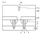
- FIGs. 13 through 15 are third through fifth cross sectional views of the conventional semiconductor device on the way of manufacture thereof.
- FIGs. 13 through 15 show the cross sectional structures of the semiconductor device in the manufacturing process subsequent to FIG. 12 .
- a step as high as the interlayer insulator film 107 thickness is caused between interlayer insulator film 107 and the semiconductor substrate exposed to contact hole 111.
- interlayer insulator film 107 When interlayer insulator film 107 is thick, e.g. 0.5 ⁇ m or thicker, the step caused between interlayer insulator film 107 and the semiconductor substrate exposed to contact hole 111 is high, impairing the step coverage of interlayer insulator film 107. If the step coverage of interlayer insulator film 107 is impaired, the growth of metal electrode layer 108 by sputtering on the side wall of contact hole 111 will delay. Due to the delayed growth, void 112 is caused locally in metal electrode layer 108. Void 112 is a concavity caused in the metal electrode layer 108 surface or a cavity caused in metal electrode layer 108. In FIG. 12 , a concavity caused in the surface of metal electrode layer 108 is shown.
- the residue of the passivation film formed on the metal electrode layer 108 surface after forming the pattern of metal electrode layer 108 also remains on the metal electrode layer 108 surface in the same manner as resist residue 114.
- residue 114 remains on the metal electrode layer 108 surface as described above, metal plating layer 109 is not formed on the portion of the metal electrode layer 108 surface, to which residue 114 is sticking as shown in FIG. 15 . Therefore, in bonding metal plating layer 109 and a wire (not shown) to each other with a solder, the solder extends to the portion of metal electrode layer 108 not covered by metal plating layer 109 and the semiconductor device may be broken down.
- organic residue 114 remaining on the metal electrode layer 108 surface impairs the electric characteristics.
- organic residue 114 remaining on the metal electrode layer 108 surface lowers the bonding strength between metal electrode layer 108 and the wire.
- residue 114 may be prevented from causing by improving the step coverage of metal electrode layer 108 to prevent void 112 from occurring. In this case however, the problems as described below will be caused.
- metal electrode layer 108 may be deposited on the front surface of the semiconductor substrate by sputtering in the state, in which the temperature of the semiconductor substrate is raised. However, when metal electrode layer 108 made of aluminum and such a metal is formed on the semiconductor substrate surface without interposing any barrier film therebetween, the semiconductor substrate and metal electrode layer 108 will be in contact with each other directly.
- Patent Document 1 proposes a method for improving the step coverage of the metal electrode layer.
- the Patent Document 1 discloses nothing on the relation between the shape of the contact hole and the interlayer insulator film thickness. Since anything is not described on the void caused in the metal electrode layer, the problems described above will be caused, if the void is caused in the metal electrode layer.
- a semiconductor device including:
- the thickness of the interlayer insulator film is 0.6 times or more as large as the second opening width of the first opening.
- the contact hole is rectangular in the planar pattern thereof, and the contact holes are arranged in parallel and perpendicular to the extending direction of the trenches.
- the contact holes parallel to each other in the direction perpendicular to the extending direction of the trenches are arranged along the extending direction of the trenches.
- the second electrode is made of a material containing aluminum as the main component thereof.
- the second electrode is 2 ⁇ m or more in thickness.
- the interlayer insulator film is 0.5 ⁇ m or more in thickness.
- electroless plating is performed to the surface of the second electrode.
- a method of manufacturing a semiconductor device including the steps of:
- the method further includes the steps of:
- the thickness of the interlayer insulator film is set to be 0.6 times or more as large as the second opening width of the first opening perpendicular to the extending direction of the trench.
- openings are formed in the resist in parallel and perpendicular to the extending direction of the trenches.
- a stripe-shaped opening extending in parallel to the extending direction of the trench is formed in the resist.
- the second electrode is made of a material containing aluminum as the main component thereof.
- the second electrode is set to be 2 ⁇ m or more in thickness.
- the interlayer insulator film is set to be 0.5 ⁇ m or more in thickness.
- the method further includes the step of:
- the step between the interlayer insulator film and the semiconductor substrate exposed to the contact hole is made to be gentle. Since the step coverage of the interlayer insulator film is improved due to the gentle step as compared with the step coverage of the interlayer insulator film according to the prior art, any void is not caused in the metal electrode layer formed on the interlayer insulator film. Therefore, the resist mask for pattering the metal electrode layer is removed without leaving any residue of the resist on the metal electrode layer. Therefore, it is possible to form a metal plating layer uniformly on the metal electrode layer.
- the semiconductor device according to the invention and the method of manufacturing a semiconductor device according to the invention facilitate improving the reliability of the semiconductor devices.
- the n-type layer or the n-type region is a layer or a region, therein electrons are majority carriers.
- the p-type layer or the p-type region is a layer or a region, therein holes are majority carriers.
- the suffix "+" on the shoulder of the letter “n” or “p” indicating the conductivity type of the layer or the region indicates that the layer or the region is doped relatively heavily.
- the suffix "-" on the shoulder of the letter “n” or “p” indicating the conductivity type of the layer or the region indicates that the layer or the region is doped relatively lightly.
- the same reference numerals are used to designate the same or similar constituent elements and their duplicated descriptions will not be made for the sake of simplicity.
- FIG. 1 is the cross sectional view of a semiconductor device according to a first embodiment of the invention. Now the semiconductor device according to the first embodiment will be described exemplary in connection with a vertical trench IGBT.
- the semiconductor device according to the first embodiment includes a front surface device structure, including gate electrode 2, gate insulator film 3, p-type channel region (p-type base region: a second semiconductor region of a second conductivity type) 4, and n + source region 5, in the front surface of the active region in a semiconductor substrate of an n-type (first conductivity type) that works as n- drift region (a first semiconductor region of the first conductivity type) 1 .
- a front surface device structure including gate electrode 2, gate insulator film 3, p-type channel region (p-type base region: a second semiconductor region of a second conductivity type) 4, and n + source region 5, in the front surface of the active region in a semiconductor substrate of an n-type (first conductivity type) that works as n- drift region (a first semiconductor region of the first conductivity
- p-type channel region 4 is formed in the surface portion on the front surface side of the semiconductor substrate.
- Trench 6 is formed through p-type channel region 4 into n - drift region 1.
- Trenches 6 are shaped with the respective stripes extending in parallel to each other in the planar pattern thereof.
- Gate electrode (first electrode) 2 is buried in trench 6 with gate insulator film 3 interposed between gate electrode 2 and trench 6.
- n + source region 5 is formed selectively.
- n + source region 5 is in contact with gate insulator film 3 formed on the side wall of trench 6.
- interlayer insulator film 7 is formed on the front surface of n - drift region 1 that is the surface opposite to the surface, through which p-type channel region 4 is in contact with n - drift region 1.
- Interlayer insulator film 7 may be an oxide film or a nitride film with no problem.
- the thickness t1 of interlayer insulator film 7 may be 0.5 ⁇ m or thicker, for example.
- Contact hole 11, e.g. for a source contact, may be formed in interlayer insulator film 7.
- Metal electrode layer (second electrode) 8 is formed on interlayer insulator film 7 and in contact hole 11.
- Metal electrode layer 8 is connected to p-type channel region 4 and n + source region 5 via contact hole 11.
- Metal electrode layer 8 is made, for example, of a material containing aluminum as the main component thereof.
- metal electrode layer 8 may be made, for example, of aluminum or an aluminum alloy with no problem.
- the thickness t2 of metal electrode layer 8 may be 2 ⁇ m or thicker with no problem.
- Metal plating layer 9 is formed on metal plating layer 8.
- Metal plating layer 9 may be a plating layer made of nickel with no problem.
- the breakdown withstanding structure (not shown) in the semiconductor substrate is formed such that the breakdown withstanding structure surrounds the active region.
- the front surface device structure of the breakdown withstanding structure such as a floating p-type semiconductor region (field limiting ring) and a field plate electrode in contact with the p-type semiconductor region is formed and a passivation film is formed on the front surface of the breakdown-withstanding structure.
- Contact hole 11 includes first opening 12 and second opening 13 connected to each other.
- First opening 12 is on the side of the boundary between interlayer insulator film 7 and metal electrode layer 8.
- the first opening width w1 on the side of the boundary between interlayer insulator film 7 and metal electrode layer 8 and perpendicular to the extending direction of trench 6 is wider than the second opening width w2 on the semiconductor substrate side and perpendicular to the extending direction of trench 6. Therefore, first opening 12 has a trapezoidal cross sectional shape, one of the parallel sides (bases) of which is on the side of the boundary between interlayer insulator film 7 and metal electrode layer 8 and the other one of the parallel sides is on the semiconductor substrate side.
- Second opening 13 is connected to the semiconductor substrate side of first opening 12 and extended through interlayer insulator film 7 such that the front surface of the semiconductor substrate is exposed to second opening 13 selectively.
- Second opening 13 is the same in width from the side of the boundary between interlayer insulator film 7 and metal electrode layer 8 to the side of the semiconductor substrate.
- the opening width of second opening 13 perpendicular to the extending direction of trench 6 is equal to the second opening width w2 of first opening 12. Therefore, second opening 13 has a rectangular cross sectional shape.
- the relations between the first and second opening widths w1 and w2 of first opening 12 and the thickness t1 of interlayer insulator film 7 will be described below. It is preferable to set the thickness t1 of interlayer insulator film 7 to be 0.28 times or less as large as the first opening width w1 of first opening 12 as expressed by the following formula (1). If interlayer insulator film 7 and first opening 12 of contact hole 11 are formed such that the dimensions thereof satisfy the formula (1), any void will not be caused in metal electrode layer 8.
- the thickness t1 of interlayer insulator film 7 may be 0.6 times or more as large as the second opening width w2 of first opening 12 with no problem.
- the contact hole is formed in the interlayer insulator film at the size that satisfies the following formula (2) in the conventional semiconductor device, voids are liable in metal electrode layer. In contrast, any void will not be caused in the electrode layer 8 in the semiconductor device according to the first embodiment, even if contact hole 11 is formed in interlayer insulator film 7 at the size thereof that satisfies the following formula (2).
- contact hole 11 By forming contact hole 11 having the above described shape and size, the bump caused in surface portion 20 of metal electrode layer 8 above contact hole 11 will not be so large as to cause any void in metal electrode layer 8, even if metal electrode layer 8 is 2 ⁇ m or more in thickness.
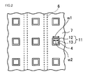
- FIG. 2 is the top plan view of the semiconductor device according to the first embodiment of the invention.
- contact hole 11 has a rectangular planar shape.
- first opening 12 and second opening 13 have respective rectangular planar shapes.
- Contact holes 11 are arranged in a planar matrix pattern in parallel and in perpendicular to the extending direction of trenches 6.
- contact holes 11 are arranged like islands regularly in parallel and in perpendicular to the extending direction of trenches 6 with an equal spacing left between contact holes 11.
- Each contact hole 11 exposes the portion of the semiconductor substrate sandwiched by trenches 6.
- p-type channel region 4 including an n + source region (not shown) formed therein and a part of the n + source region formed in p-type channel region 4 are exposed to contact hole 11.
- rectangular trenches may be arranged in a planar matrix pattern, in place of trenches 6 extending in parallel to each other in the planar stripe pattern thereof, such that the rectangular trenches sandwich p-type channel region 4 exposed to contact hole 11 arranged in a planar matrix pattern.
- FIG. 3 is the top plan view of a semiconductor device according to a second embodiment of the invention.
- contact holes 31 extending in parallel to the extending direction of trench 6 are formed in interlayer insulator film 37 such that contact holes 31 are arranged in a planar stripe pattern.
- First opening 32 and second opening 33 extend in parallel to the extending direction of trench 6.
- Contact hole 31 is arranged between adjacent trenches 6.
- the portion of p-type channel region 4 sandwiched by trenches 6 is exposed to contact hole 31.
- the portions of p-type channel regions 4 sandwiched by trenches 6 are exposed as the respective stripes extending in parallel to the extending direction of trenches 6.
- contact hole 31 shown in FIG. 3 except the planar shape thereof is the same with the structure of contact hole 11 shown in FIG. 2 .
- a second opening (not shown), the width thereof perpendicular to the extending direction of trench 6 is equal to the second opening width w2 of first opening 32 perpendicular to the extending direction of trench 6, is arranged on the semiconductor substrate side of first opening 32.
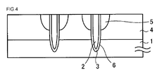
- FIGs. 4 through 9 are cross sectional views of the semiconductor device according to the first or second embodiment on the way of the manufacture thereof.
- a front surface device structure including gate electrode 2, gate insulator film 3, p-type channel region 4, and n + source region 5, is formed through the general manufacturing process in the front surface of the active region in a semiconductor substrate that will work as n- drift region 1 as shown in FIG. 4 .
- the front surface device structure (not shown) of a breakdown-withstanding structure is formed such that the breakdown-withstanding structure surrounds the active region.
- trench 6 is formed through p-type channel region 4 into n- drift region 1. Then, gate electrode 2 is buried in trench 6 with gate insulator film 3 interposed between gate electrode 2 and the side wall of trench 6. Then, n + source region 5 is formed in the surface portion on the front surface side of the semiconductor substrate.
- interlayer insulator film 7 is formed on the front surface of the semiconductor substrate by chemical vapor deposition (hereinafter referred to as "CVD") as shown in FIG. 5 .
- CVD chemical vapor deposition
- resist mask 41 including opening 42, to which the intended formation region for forming contact hole 11 therein is exposed is formed on interlayer insulator film 7.
- the opening width w3 of opening 42 is almost the same with the second opening width w2 of first opening 12 formed using resist mask 41 for a mask in the late step.
- Opening 42 of resist mask 41 is formed such that the contact holes formed in the late step using resist mask 41 for a mask may be arranged in a planar matrix pattern or a planar stripe pattern.
- openings 42 are arranged in a planar matrix pattern, in which openings 42 are arranged in parallel and in perpendicular to the extending direction of trench 6 (cf. FIG. 2 ).
- openings 42 are arranged in a planar stripe pattern, in which openings 42 extend in parallel to the extending direction of trench 6 (cf. FIG. 3 ).
- interlayer insulator film 7 exposed to opening 42 of resist mask 41 is removed by isotropic etching using resist mask 41 for a mask.
- first opening 12 shallower than the thickness of interlayer insulator film 7 is formed in the surface portion of interlayer insulator film 7.
- interlayer insulator film 7 is removed by isotropic etching such that the first opening 12 depth is from 50 % to 60 % of the interlayer insulator film 7 thickness.
- first opening width w1 of first opening 12 on the resist mask 41 side is wider than the opening width of opening 42 in resist mask 41 and the opening width (second opening width w2) of first opening 12 on the semiconductor substrate side is set to be almost equal to the opening 42 width in resist mask 41. Therefore, first opening 12 has a trapezoidal cross sectional shape.
- a chemical dry etching (hereinafter referred to "CDE") apparatus may be used for the isotropic etching with no problem.
- anisotropic etching is conducted using resist mask 41 employed in forming first opening 12 to remove interlayer insulator film 7 exposed to opening 42 in resist mask 41.
- the anisotropic etching for forming second opening 13 is conducted until the front surface of the semiconductor substrate is exposed.
- anisotropic etching conducted as described above interlayer insulator film 7 exposed to first opening 12 is removed and second opening 13 connected to first opening 12 is formed.
- second opening 13 is formed at the opening 42 width in resist mask 41, that is the opening width the same with the second opening width w2 of first opening 12 in the depth direction of interlayer insulator film 7. Therefore, the cross sectional shape of second opening 13 is rectangular.
- contact hole 11 including first opening 12 and second opening 13 is formed as shown in FIG. 8 .
- contact hole 11 including n + source region 5 formed therein and a part of n + source region 5 formed in p-type channel region 4 are exposed.
- resist mask 41 is removed by an ashing treatment using plasma, for example.
- metal electrode layer 8 made e.g. of aluminum, is deposited by sputtering on interlayer insulator film 7.
- Metal electrode layer 8 is buried in contact hole 11 and connected to p-type channel region 4 and n + source region 5 through contact hole 11.
- a resist mask (not shown), in which the pattern of metal electrode layer 8 is formed, is formed on metal electrode layer 8. Then, using the resist mask for a mask, metal electrode layer 8 exposed to the opening in the rest mask is removed to obtain the desired metal electrode layer 8 pattern. Then, the resist mask used for patterning metal electrode layer 8 is removed by a plasma ashing treatment, for example. Then, a thermal annealing treatment is conducted to obtain a stable adhesion of metal electrode layer 8 and excellent electric characteristics.
- a passivation film (not shown) is formed on the front surface of the semiconductor substrate. Then, the passivation film is patterned by photolithography to expose metal electrode layer 8. Then, a pretreatment and a zincate treatment are conducted for forming metal plating layer 9 on the surface of metal electrode layer 8. Metal plating layer 9, made e.g. of nickel, is formed by electroless plating on the surface of metal electrode layer 8. Then, a collector region and a back surface electrode (not shown) are formed on the back surface of the semiconductor substrate. Thus, a vertical trench IGBT as shown in FIG. 1 is completed.
- the first opening width w1 of first opening 12, that constitutes contact hole 11, on the side of the boundary between interlayer insulator film 7 and metal electrode layer 8 is formed to be wider than the second opening width w2 on the semiconductor substrate side.
- the angle between the side wall of first opening 12 and the front surface of the semiconductor substrate exposed to contact hole 11 is obtuse. Therefore, the step caused between interlayer insulator film 7 and the semiconductor substrate exposed to contact hole 11 curves more gently than the step caused in the conventional semiconductor device due to the side wall of first opening 12 slanting to the front surface of the semiconductor substrate at an obtuse angle.
- the step caused between interlayer insulator film 7 and the semiconductor substrate exposed to contact hole 11 is made to slant more gently than the step caused in the conventional semiconductor device. Since the step coverage of interlayer insulator film 7 is improved as compared with the step coverage in the conventional semiconductor device, any void is not caused in metal electrode layer 8 formed on interlayer insulator film 7. Therefore, it is possible to remove the resist mask for patterning metal electrode layer 8 without leaving any residue of the resist on metal electrode layer 8. Therefore, metal plating layer 9 is formed uniformly on metal electrode layer 8 and the reliability of the semiconductor device is improved.
- FIG. 10 is a graph relating the void generation rate with the contact hole shape.
- the semiconductor devices hereinafter referred to as the "specimens" according to the second embodiment which include contact holes 31 arranged in a planar stripe pattern are fabricated (manufactured).
- the first opening width w1 of the specimens is changed variously.
- the first opening width w1 of first opening 32 is set in the range, in which the thickness t1 of interlayer insulator film 37 is from 0.25 times to 0.32 times as large as the first opening width w1 of first opening 32. (In other words, the thickness/opening width ratio, defined as t1/w1, is set at a value between 0.25 and 0.32.)
- second opening width w2 of first opening 32 is set at a value, at which the thickness t1 of interlayer insulator film 37 is 0.6 times as large as the second opening width w2 of first opening 32.
- the depths of first opening 32 and the second opening are different depending on the first opening width w1 of first opening 32 formed by isotropic etching. Void generation is investigated in the specimens manufactured under the conditions described above.
- the semiconductor device according to the first embodiment of the invention includes contact holes 11 arranged in a planar matrix pattern.
- the semiconductor device according to the second embodiment includes contact holes 31 arranged in a planar stripe pattern. If the thickness t1 of interlayer insulator film 7 and the first opening width w1 of first opening 12 is set such that the thickness/opening width ratio is 0.28 or less in the semiconductor device according to the first embodiment, the semiconductor device according to the first embodiment will exhibit the effects the same with the effects, which the semiconductor device according to the second embodiment exhibits.
- the invention has been described above in connection with a vertical trench IGBT, the invention is applicable to semiconductor devices having various structures including a metal electrode layer on a semiconductor substrate.
- the first conductivity type is an n-type and the second conductivity type is a p-type in the above description, the first conductivity type may be a p-type and the second conductivity type may be an n-type with no problem.
- the semiconductor device according to the invention and the method for manufacturing the semiconductor device according to the invention are useful for the semiconductor device that includes a thick aluminum electrode on the front surface of a semiconductor substrate and for the manufacture thereof.
Landscapes
- Electrodes Of Semiconductors (AREA)
- Internal Circuitry In Semiconductor Integrated Circuit Devices (AREA)
Applications Claiming Priority (1)
| Application Number | Priority Date | Filing Date | Title |
|---|---|---|---|
| JP2011236849A JP6099302B2 (ja) | 2011-10-28 | 2011-10-28 | 半導体装置の製造方法 |
Publications (3)
| Publication Number | Publication Date |
|---|---|
| EP2587544A2 true EP2587544A2 (de) | 2013-05-01 |
| EP2587544A3 EP2587544A3 (de) | 2017-11-01 |
| EP2587544B1 EP2587544B1 (de) | 2022-04-20 |
Family
ID=47263066
Family Applications (1)
| Application Number | Title | Priority Date | Filing Date |
|---|---|---|---|
| EP12189428.1A Active EP2587544B1 (de) | 2011-10-28 | 2012-10-22 | Halbleiterbauelement und Verfahren zu seiner Herstellung |
Country Status (4)
| Country | Link |
|---|---|
| US (1) | US9362373B2 (de) |
| EP (1) | EP2587544B1 (de) |
| JP (1) | JP6099302B2 (de) |
| CN (1) | CN103094330B (de) |
Families Citing this family (4)
| Publication number | Priority date | Publication date | Assignee | Title |
|---|---|---|---|---|
| JP6296970B2 (ja) * | 2014-12-12 | 2018-03-20 | 三菱電機株式会社 | 半導体装置及びその製造方法 |
| CN110383488B (zh) * | 2017-03-16 | 2023-08-29 | 三菱电机株式会社 | 半导体装置 |
| CN108630540B (zh) * | 2017-03-24 | 2021-05-28 | 中芯国际集成电路制造(上海)有限公司 | 半导体装置及其制造方法 |
| JPWO2020144790A1 (ja) * | 2019-01-10 | 2021-02-18 | 三菱電機株式会社 | 電力用半導体装置 |
Family Cites Families (18)
| Publication number | Priority date | Publication date | Assignee | Title |
|---|---|---|---|---|
| JP3481287B2 (ja) * | 1994-02-24 | 2003-12-22 | 三菱電機株式会社 | 半導体装置の製造方法 |
| JP3724110B2 (ja) * | 1997-04-24 | 2005-12-07 | 三菱電機株式会社 | 半導体装置の製造方法 |
| JPH1140514A (ja) * | 1997-07-23 | 1999-02-12 | Sanyo Electric Co Ltd | 半導体装置の製造方法 |
| US6211071B1 (en) * | 1999-04-22 | 2001-04-03 | Advanced Micro Devices, Inc. | Optimized trench/via profile for damascene filling |
| US6649973B2 (en) * | 2001-03-28 | 2003-11-18 | Rohm Co., Ltd. | Semiconductor device and method for manufacturing the same |
| JP2003152075A (ja) | 2001-11-09 | 2003-05-23 | Sony Corp | 半導体装置の製造方法 |
| US6828160B2 (en) * | 2002-06-11 | 2004-12-07 | Winbond Electronics Corporation | Method of forming ferroelectric random access memory cell |
| JP3819337B2 (ja) * | 2002-07-25 | 2006-09-06 | 三菱電機株式会社 | 半導体装置の製造方法 |
| US20050181618A1 (en) * | 2004-02-17 | 2005-08-18 | Northrop Grumman Space & Mission Systems Corporation | Polymer via etching process |
| JP3906213B2 (ja) * | 2004-03-10 | 2007-04-18 | 株式会社東芝 | 半導体装置 |
| JP2005303218A (ja) * | 2004-04-16 | 2005-10-27 | Renesas Technology Corp | 半導体装置およびその製造方法 |
| US7456097B1 (en) * | 2004-11-30 | 2008-11-25 | National Semiconductor Corporation | System and method for faceting via top corners to improve metal fill |
| JP2007149867A (ja) * | 2005-11-25 | 2007-06-14 | Toyota Industries Corp | 半導体装置 |
| US7723851B2 (en) * | 2007-09-11 | 2010-05-25 | International Business Machines Corporation | Method of fabricating ultra-deep vias and three-dimensional integrated circuits using ultra-deep vias |
| US8207612B2 (en) * | 2007-11-09 | 2012-06-26 | Sanken Electric Co., Ltd. | Semiconductor device and manufacturing method thereof |
| KR20090070785A (ko) * | 2007-12-27 | 2009-07-01 | 주식회사 동부하이텍 | 반도체 소자의 제조 방법 |
| JP2010129585A (ja) * | 2008-11-25 | 2010-06-10 | Toyota Motor Corp | 半導体装置の製造方法 |
| JP5560595B2 (ja) * | 2009-06-18 | 2014-07-30 | 富士電機株式会社 | 半導体装置の製造方法 |
-
2011
- 2011-10-28 JP JP2011236849A patent/JP6099302B2/ja active Active
-
2012
- 2012-10-22 EP EP12189428.1A patent/EP2587544B1/de active Active
- 2012-10-26 US US13/661,105 patent/US9362373B2/en active Active
- 2012-10-26 CN CN201210415195.7A patent/CN103094330B/zh active Active
Non-Patent Citations (1)
| Title |
|---|
| None |
Also Published As
| Publication number | Publication date |
|---|---|
| EP2587544B1 (de) | 2022-04-20 |
| JP2013098203A (ja) | 2013-05-20 |
| US20130105856A1 (en) | 2013-05-02 |
| EP2587544A3 (de) | 2017-11-01 |
| CN103094330A (zh) | 2013-05-08 |
| CN103094330B (zh) | 2017-05-03 |
| US9362373B2 (en) | 2016-06-07 |
| JP6099302B2 (ja) | 2017-03-22 |
Similar Documents
| Publication | Publication Date | Title |
|---|---|---|
| JP6835241B2 (ja) | 半導体装置 | |
| US8946726B2 (en) | Grid-UMOSFET with electric field shielding of gate oxide | |
| US10229969B2 (en) | Power semiconductor device | |
| EP2701201A1 (de) | Halbleitervorrichtung und herstellungsverfahren dafür | |
| CN101834203A (zh) | 半导体装置及半导体装置的制造方法 | |
| US11489047B2 (en) | Semiconductor device and method of manufacturing the same | |
| EP3024018B1 (de) | Halbleiterbauelement | |
| EP2587544B1 (de) | Halbleiterbauelement und Verfahren zu seiner Herstellung | |
| US12471335B2 (en) | Silicon carbide semiconductor device including semiconductor element having gate-trench structure | |
| EP3832698A1 (de) | Halbleiterbauelement und herstellungsverfahren dafür | |
| CN109564876B (zh) | 半导体装置 | |
| RU2702405C1 (ru) | Полупроводниковое устройство | |
| JP2016012740A (ja) | 半導体装置および半導体装置の製造方法 | |
| JP6741091B2 (ja) | 半導体装置の製造方法 | |
| JP6264586B2 (ja) | 半導体装置の製造方法および半導体装置 | |
| JP6190083B2 (ja) | 縦型トレンチigbtおよびその製造方法 | |
| JP6496925B2 (ja) | 半導体装置および半導体装置の製造方法 | |
| JP7666114B2 (ja) | 半導体装置 | |
| JP2019091912A (ja) | 半導体装置 | |
| JP2025122595A (ja) | 半導体装置 | |
| JP2026000789A (ja) | 半導体装置 |
Legal Events
| Date | Code | Title | Description |
|---|---|---|---|
| PUAI | Public reference made under article 153(3) epc to a published international application that has entered the european phase |
Free format text: ORIGINAL CODE: 0009012 |
|
| AK | Designated contracting states |
Kind code of ref document: A2 Designated state(s): AL AT BE BG CH CY CZ DE DK EE ES FI FR GB GR HR HU IE IS IT LI LT LU LV MC MK MT NL NO PL PT RO RS SE SI SK SM TR |
|
| AX | Request for extension of the european patent |
Extension state: BA ME |
|
| PUAL | Search report despatched |
Free format text: ORIGINAL CODE: 0009013 |
|
| AK | Designated contracting states |
Kind code of ref document: A3 Designated state(s): AL AT BE BG CH CY CZ DE DK EE ES FI FR GB GR HR HU IE IS IT LI LT LU LV MC MK MT NL NO PL PT RO RS SE SI SK SM TR |
|
| AX | Request for extension of the european patent |
Extension state: BA ME |
|
| RIC1 | Information provided on ipc code assigned before grant |
Ipc: H01L 29/739 20060101AFI20170926BHEP Ipc: H01L 29/417 20060101ALI20170926BHEP Ipc: H01L 29/66 20060101ALI20170926BHEP |
|
| STAA | Information on the status of an ep patent application or granted ep patent |
Free format text: STATUS: REQUEST FOR EXAMINATION WAS MADE |
|
| 17P | Request for examination filed |
Effective date: 20180502 |
|
| RBV | Designated contracting states (corrected) |
Designated state(s): AL AT BE BG CH CY CZ DE DK EE ES FI FR GB GR HR HU IE IS IT LI LT LU LV MC MK MT NL NO PL PT RO RS SE SI SK SM TR |
|
| STAA | Information on the status of an ep patent application or granted ep patent |
Free format text: STATUS: EXAMINATION IS IN PROGRESS |
|
| 17Q | First examination report despatched |
Effective date: 20200511 |
|
| GRAP | Despatch of communication of intention to grant a patent |
Free format text: ORIGINAL CODE: EPIDOSNIGR1 |
|
| STAA | Information on the status of an ep patent application or granted ep patent |
Free format text: STATUS: GRANT OF PATENT IS INTENDED |
|
| RIC1 | Information provided on ipc code assigned before grant |
Ipc: H01L 21/331 20060101ALI20211005BHEP Ipc: H01L 29/417 20060101ALI20211005BHEP Ipc: H01L 29/06 20060101ALI20211005BHEP Ipc: H01L 29/739 20060101AFI20211005BHEP |
|
| INTG | Intention to grant announced |
Effective date: 20211102 |
|
| GRAS | Grant fee paid |
Free format text: ORIGINAL CODE: EPIDOSNIGR3 |
|
| GRAA | (expected) grant |
Free format text: ORIGINAL CODE: 0009210 |
|
| STAA | Information on the status of an ep patent application or granted ep patent |
Free format text: STATUS: THE PATENT HAS BEEN GRANTED |
|
| AK | Designated contracting states |
Kind code of ref document: B1 Designated state(s): AL AT BE BG CH CY CZ DE DK EE ES FI FR GB GR HR HU IE IS IT LI LT LU LV MC MK MT NL NO PL PT RO RS SE SI SK SM TR |
|
| REG | Reference to a national code |
Ref country code: GB Ref legal event code: FG4D |
|
| REG | Reference to a national code |
Ref country code: CH Ref legal event code: EP |
|
| REG | Reference to a national code |
Ref country code: DE Ref legal event code: R096 Ref document number: 602012078060 Country of ref document: DE |
|
| REG | Reference to a national code |
Ref country code: IE Ref legal event code: FG4D |
|
| REG | Reference to a national code |
Ref country code: AT Ref legal event code: REF Ref document number: 1485886 Country of ref document: AT Kind code of ref document: T Effective date: 20220515 |
|
| REG | Reference to a national code |
Ref country code: LT Ref legal event code: MG9D |
|
| REG | Reference to a national code |
Ref country code: NL Ref legal event code: MP Effective date: 20220420 |
|
| REG | Reference to a national code |
Ref country code: AT Ref legal event code: MK05 Ref document number: 1485886 Country of ref document: AT Kind code of ref document: T Effective date: 20220420 |
|
| PG25 | Lapsed in a contracting state [announced via postgrant information from national office to epo] |
Ref country code: NL Free format text: LAPSE BECAUSE OF FAILURE TO SUBMIT A TRANSLATION OF THE DESCRIPTION OR TO PAY THE FEE WITHIN THE PRESCRIBED TIME-LIMIT Effective date: 20220420 |
|
| PG25 | Lapsed in a contracting state [announced via postgrant information from national office to epo] |
Ref country code: SE Free format text: LAPSE BECAUSE OF FAILURE TO SUBMIT A TRANSLATION OF THE DESCRIPTION OR TO PAY THE FEE WITHIN THE PRESCRIBED TIME-LIMIT Effective date: 20220420 Ref country code: PT Free format text: LAPSE BECAUSE OF FAILURE TO SUBMIT A TRANSLATION OF THE DESCRIPTION OR TO PAY THE FEE WITHIN THE PRESCRIBED TIME-LIMIT Effective date: 20220822 Ref country code: NO Free format text: LAPSE BECAUSE OF FAILURE TO SUBMIT A TRANSLATION OF THE DESCRIPTION OR TO PAY THE FEE WITHIN THE PRESCRIBED TIME-LIMIT Effective date: 20220720 Ref country code: LT Free format text: LAPSE BECAUSE OF FAILURE TO SUBMIT A TRANSLATION OF THE DESCRIPTION OR TO PAY THE FEE WITHIN THE PRESCRIBED TIME-LIMIT Effective date: 20220420 Ref country code: HR Free format text: LAPSE BECAUSE OF FAILURE TO SUBMIT A TRANSLATION OF THE DESCRIPTION OR TO PAY THE FEE WITHIN THE PRESCRIBED TIME-LIMIT Effective date: 20220420 Ref country code: GR Free format text: LAPSE BECAUSE OF FAILURE TO SUBMIT A TRANSLATION OF THE DESCRIPTION OR TO PAY THE FEE WITHIN THE PRESCRIBED TIME-LIMIT Effective date: 20220721 Ref country code: FI Free format text: LAPSE BECAUSE OF FAILURE TO SUBMIT A TRANSLATION OF THE DESCRIPTION OR TO PAY THE FEE WITHIN THE PRESCRIBED TIME-LIMIT Effective date: 20220420 Ref country code: ES Free format text: LAPSE BECAUSE OF FAILURE TO SUBMIT A TRANSLATION OF THE DESCRIPTION OR TO PAY THE FEE WITHIN THE PRESCRIBED TIME-LIMIT Effective date: 20220420 Ref country code: BG Free format text: LAPSE BECAUSE OF FAILURE TO SUBMIT A TRANSLATION OF THE DESCRIPTION OR TO PAY THE FEE WITHIN THE PRESCRIBED TIME-LIMIT Effective date: 20220720 Ref country code: AT Free format text: LAPSE BECAUSE OF FAILURE TO SUBMIT A TRANSLATION OF THE DESCRIPTION OR TO PAY THE FEE WITHIN THE PRESCRIBED TIME-LIMIT Effective date: 20220420 |
|
| PG25 | Lapsed in a contracting state [announced via postgrant information from national office to epo] |
Ref country code: RS Free format text: LAPSE BECAUSE OF FAILURE TO SUBMIT A TRANSLATION OF THE DESCRIPTION OR TO PAY THE FEE WITHIN THE PRESCRIBED TIME-LIMIT Effective date: 20220420 Ref country code: PL Free format text: LAPSE BECAUSE OF FAILURE TO SUBMIT A TRANSLATION OF THE DESCRIPTION OR TO PAY THE FEE WITHIN THE PRESCRIBED TIME-LIMIT Effective date: 20220420 Ref country code: LV Free format text: LAPSE BECAUSE OF FAILURE TO SUBMIT A TRANSLATION OF THE DESCRIPTION OR TO PAY THE FEE WITHIN THE PRESCRIBED TIME-LIMIT Effective date: 20220420 Ref country code: IS Free format text: LAPSE BECAUSE OF FAILURE TO SUBMIT A TRANSLATION OF THE DESCRIPTION OR TO PAY THE FEE WITHIN THE PRESCRIBED TIME-LIMIT Effective date: 20220820 |
|
| REG | Reference to a national code |
Ref country code: DE Ref legal event code: R097 Ref document number: 602012078060 Country of ref document: DE |
|
| PG25 | Lapsed in a contracting state [announced via postgrant information from national office to epo] |
Ref country code: SM Free format text: LAPSE BECAUSE OF FAILURE TO SUBMIT A TRANSLATION OF THE DESCRIPTION OR TO PAY THE FEE WITHIN THE PRESCRIBED TIME-LIMIT Effective date: 20220420 Ref country code: SK Free format text: LAPSE BECAUSE OF FAILURE TO SUBMIT A TRANSLATION OF THE DESCRIPTION OR TO PAY THE FEE WITHIN THE PRESCRIBED TIME-LIMIT Effective date: 20220420 Ref country code: RO Free format text: LAPSE BECAUSE OF FAILURE TO SUBMIT A TRANSLATION OF THE DESCRIPTION OR TO PAY THE FEE WITHIN THE PRESCRIBED TIME-LIMIT Effective date: 20220420 Ref country code: EE Free format text: LAPSE BECAUSE OF FAILURE TO SUBMIT A TRANSLATION OF THE DESCRIPTION OR TO PAY THE FEE WITHIN THE PRESCRIBED TIME-LIMIT Effective date: 20220420 Ref country code: DK Free format text: LAPSE BECAUSE OF FAILURE TO SUBMIT A TRANSLATION OF THE DESCRIPTION OR TO PAY THE FEE WITHIN THE PRESCRIBED TIME-LIMIT Effective date: 20220420 Ref country code: CZ Free format text: LAPSE BECAUSE OF FAILURE TO SUBMIT A TRANSLATION OF THE DESCRIPTION OR TO PAY THE FEE WITHIN THE PRESCRIBED TIME-LIMIT Effective date: 20220420 |
|
| PLBE | No opposition filed within time limit |
Free format text: ORIGINAL CODE: 0009261 |
|
| STAA | Information on the status of an ep patent application or granted ep patent |
Free format text: STATUS: NO OPPOSITION FILED WITHIN TIME LIMIT |
|
| 26N | No opposition filed |
Effective date: 20230123 |
|
| PG25 | Lapsed in a contracting state [announced via postgrant information from national office to epo] |
Ref country code: AL Free format text: LAPSE BECAUSE OF FAILURE TO SUBMIT A TRANSLATION OF THE DESCRIPTION OR TO PAY THE FEE WITHIN THE PRESCRIBED TIME-LIMIT Effective date: 20220420 |
|
| PG25 | Lapsed in a contracting state [announced via postgrant information from national office to epo] |
Ref country code: SI Free format text: LAPSE BECAUSE OF FAILURE TO SUBMIT A TRANSLATION OF THE DESCRIPTION OR TO PAY THE FEE WITHIN THE PRESCRIBED TIME-LIMIT Effective date: 20220420 Ref country code: MC Free format text: LAPSE BECAUSE OF FAILURE TO SUBMIT A TRANSLATION OF THE DESCRIPTION OR TO PAY THE FEE WITHIN THE PRESCRIBED TIME-LIMIT Effective date: 20220420 |
|
| REG | Reference to a national code |
Ref country code: CH Ref legal event code: PL |
|
| REG | Reference to a national code |
Ref country code: BE Ref legal event code: MM Effective date: 20221031 |
|
| GBPC | Gb: european patent ceased through non-payment of renewal fee |
Effective date: 20221022 |
|
| PG25 | Lapsed in a contracting state [announced via postgrant information from national office to epo] |
Ref country code: LU Free format text: LAPSE BECAUSE OF NON-PAYMENT OF DUE FEES Effective date: 20221022 |
|
| PG25 | Lapsed in a contracting state [announced via postgrant information from national office to epo] |
Ref country code: LI Free format text: LAPSE BECAUSE OF NON-PAYMENT OF DUE FEES Effective date: 20221031 Ref country code: FR Free format text: LAPSE BECAUSE OF NON-PAYMENT OF DUE FEES Effective date: 20221031 Ref country code: CH Free format text: LAPSE BECAUSE OF NON-PAYMENT OF DUE FEES Effective date: 20221031 |
|
| PG25 | Lapsed in a contracting state [announced via postgrant information from national office to epo] |
Ref country code: BE Free format text: LAPSE BECAUSE OF NON-PAYMENT OF DUE FEES Effective date: 20221031 |
|
| PG25 | Lapsed in a contracting state [announced via postgrant information from national office to epo] |
Ref country code: IE Free format text: LAPSE BECAUSE OF NON-PAYMENT OF DUE FEES Effective date: 20221022 Ref country code: GB Free format text: LAPSE BECAUSE OF NON-PAYMENT OF DUE FEES Effective date: 20221022 |
|
| PG25 | Lapsed in a contracting state [announced via postgrant information from national office to epo] |
Ref country code: IT Free format text: LAPSE BECAUSE OF FAILURE TO SUBMIT A TRANSLATION OF THE DESCRIPTION OR TO PAY THE FEE WITHIN THE PRESCRIBED TIME-LIMIT Effective date: 20220420 |
|
| PG25 | Lapsed in a contracting state [announced via postgrant information from national office to epo] |
Ref country code: HU Free format text: LAPSE BECAUSE OF FAILURE TO SUBMIT A TRANSLATION OF THE DESCRIPTION OR TO PAY THE FEE WITHIN THE PRESCRIBED TIME-LIMIT; INVALID AB INITIO Effective date: 20121022 |
|
| PG25 | Lapsed in a contracting state [announced via postgrant information from national office to epo] |
Ref country code: CY Free format text: LAPSE BECAUSE OF FAILURE TO SUBMIT A TRANSLATION OF THE DESCRIPTION OR TO PAY THE FEE WITHIN THE PRESCRIBED TIME-LIMIT Effective date: 20220420 |
|
| PG25 | Lapsed in a contracting state [announced via postgrant information from national office to epo] |
Ref country code: MK Free format text: LAPSE BECAUSE OF FAILURE TO SUBMIT A TRANSLATION OF THE DESCRIPTION OR TO PAY THE FEE WITHIN THE PRESCRIBED TIME-LIMIT Effective date: 20220420 |
|
| PG25 | Lapsed in a contracting state [announced via postgrant information from national office to epo] |
Ref country code: TR Free format text: LAPSE BECAUSE OF FAILURE TO SUBMIT A TRANSLATION OF THE DESCRIPTION OR TO PAY THE FEE WITHIN THE PRESCRIBED TIME-LIMIT Effective date: 20220420 |
|
| PG25 | Lapsed in a contracting state [announced via postgrant information from national office to epo] |
Ref country code: MT Free format text: LAPSE BECAUSE OF FAILURE TO SUBMIT A TRANSLATION OF THE DESCRIPTION OR TO PAY THE FEE WITHIN THE PRESCRIBED TIME-LIMIT Effective date: 20220420 |
|
| PG25 | Lapsed in a contracting state [announced via postgrant information from national office to epo] |
Ref country code: BG Free format text: LAPSE BECAUSE OF FAILURE TO SUBMIT A TRANSLATION OF THE DESCRIPTION OR TO PAY THE FEE WITHIN THE PRESCRIBED TIME-LIMIT Effective date: 20220420 |
|
| REG | Reference to a national code |
Ref country code: DE Ref legal event code: R079 Ref document number: 602012078060 Country of ref document: DE Free format text: PREVIOUS MAIN CLASS: H01L0029739000 Ipc: H10D0012000000 |
|
| PG25 | Lapsed in a contracting state [announced via postgrant information from national office to epo] |
Ref country code: BG Free format text: LAPSE BECAUSE OF FAILURE TO SUBMIT A TRANSLATION OF THE DESCRIPTION OR TO PAY THE FEE WITHIN THE PRESCRIBED TIME-LIMIT Effective date: 20220420 |
|
| PGFP | Annual fee paid to national office [announced via postgrant information from national office to epo] |
Ref country code: DE Payment date: 20250902 Year of fee payment: 14 |